JP2024121394A - 半導体装置 - Google Patents
半導体装置 Download PDFInfo
- Publication number
- JP2024121394A JP2024121394A JP2023028476A JP2023028476A JP2024121394A JP 2024121394 A JP2024121394 A JP 2024121394A JP 2023028476 A JP2023028476 A JP 2023028476A JP 2023028476 A JP2023028476 A JP 2023028476A JP 2024121394 A JP2024121394 A JP 2024121394A
- Authority
- JP
- Japan
- Prior art keywords
- layer
- insulating layer
- oxide semiconductor
- gate insulating
- semiconductor layer
- Prior art date
- Legal status (The legal status is an assumption and is not a legal conclusion. Google has not performed a legal analysis and makes no representation as to the accuracy of the status listed.)
- Pending
Links
Images


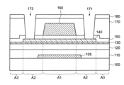


Classifications
-
- H—ELECTRICITY
- H10—SEMICONDUCTOR DEVICES; ELECTRIC SOLID-STATE DEVICES NOT OTHERWISE PROVIDED FOR
- H10D—INORGANIC ELECTRIC SEMICONDUCTOR DEVICES
- H10D64/00—Electrodes of devices having potential barriers
- H10D64/20—Electrodes characterised by their shapes, relative sizes or dispositions
- H10D64/27—Electrodes not carrying the current to be rectified, amplified, oscillated or switched, e.g. gates
- H10D64/311—Gate electrodes for field-effect devices
- H10D64/411—Gate electrodes for field-effect devices for FETs
- H10D64/511—Gate electrodes for field-effect devices for FETs for IGFETs
- H10D64/512—Disposition of the gate electrodes, e.g. buried gates
-
- H—ELECTRICITY
- H10—SEMICONDUCTOR DEVICES; ELECTRIC SOLID-STATE DEVICES NOT OTHERWISE PROVIDED FOR
- H10D—INORGANIC ELECTRIC SEMICONDUCTOR DEVICES
- H10D30/00—Field-effect transistors [FET]
- H10D30/60—Insulated-gate field-effect transistors [IGFET]
- H10D30/67—Thin-film transistors [TFT]
- H10D30/6729—Thin-film transistors [TFT] characterised by the electrodes
- H10D30/673—Thin-film transistors [TFT] characterised by the electrodes characterised by the shapes, relative sizes or dispositions of the gate electrodes
-
- H—ELECTRICITY
- H10—SEMICONDUCTOR DEVICES; ELECTRIC SOLID-STATE DEVICES NOT OTHERWISE PROVIDED FOR
- H10D—INORGANIC ELECTRIC SEMICONDUCTOR DEVICES
- H10D30/00—Field-effect transistors [FET]
- H10D30/60—Insulated-gate field-effect transistors [IGFET]
- H10D30/67—Thin-film transistors [TFT]
- H10D30/6729—Thin-film transistors [TFT] characterised by the electrodes
- H10D30/673—Thin-film transistors [TFT] characterised by the electrodes characterised by the shapes, relative sizes or dispositions of the gate electrodes
- H10D30/6733—Multi-gate TFTs
- H10D30/6734—Multi-gate TFTs having gate electrodes arranged on both top and bottom sides of the channel, e.g. dual-gate TFTs
-
- H—ELECTRICITY
- H10—SEMICONDUCTOR DEVICES; ELECTRIC SOLID-STATE DEVICES NOT OTHERWISE PROVIDED FOR
- H10D—INORGANIC ELECTRIC SEMICONDUCTOR DEVICES
- H10D30/00—Field-effect transistors [FET]
- H10D30/60—Insulated-gate field-effect transistors [IGFET]
- H10D30/67—Thin-film transistors [TFT]
- H10D30/6729—Thin-film transistors [TFT] characterised by the electrodes
- H10D30/6737—Thin-film transistors [TFT] characterised by the electrodes characterised by the electrode materials
- H10D30/6739—Conductor-insulator-semiconductor electrodes
-
- H—ELECTRICITY
- H10—SEMICONDUCTOR DEVICES; ELECTRIC SOLID-STATE DEVICES NOT OTHERWISE PROVIDED FOR
- H10D—INORGANIC ELECTRIC SEMICONDUCTOR DEVICES
- H10D30/00—Field-effect transistors [FET]
- H10D30/60—Insulated-gate field-effect transistors [IGFET]
- H10D30/67—Thin-film transistors [TFT]
- H10D30/674—Thin-film transistors [TFT] characterised by the active materials
- H10D30/6755—Oxide semiconductors, e.g. zinc oxide, copper aluminium oxide or cadmium stannate
-
- H—ELECTRICITY
- H10—SEMICONDUCTOR DEVICES; ELECTRIC SOLID-STATE DEVICES NOT OTHERWISE PROVIDED FOR
- H10D—INORGANIC ELECTRIC SEMICONDUCTOR DEVICES
- H10D30/00—Field-effect transistors [FET]
- H10D30/60—Insulated-gate field-effect transistors [IGFET]
- H10D30/67—Thin-film transistors [TFT]
- H10D30/6757—Thin-film transistors [TFT] characterised by the structure of the channel, e.g. transverse or longitudinal shape or doping profile
-
- H—ELECTRICITY
- H10—SEMICONDUCTOR DEVICES; ELECTRIC SOLID-STATE DEVICES NOT OTHERWISE PROVIDED FOR
- H10D—INORGANIC ELECTRIC SEMICONDUCTOR DEVICES
- H10D86/00—Integrated devices formed in or on insulating or conducting substrates, e.g. formed in silicon-on-insulator [SOI] substrates or on stainless steel or glass substrates
- H10D86/40—Integrated devices formed in or on insulating or conducting substrates, e.g. formed in silicon-on-insulator [SOI] substrates or on stainless steel or glass substrates characterised by multiple TFTs
-
- H—ELECTRICITY
- H10—SEMICONDUCTOR DEVICES; ELECTRIC SOLID-STATE DEVICES NOT OTHERWISE PROVIDED FOR
- H10D—INORGANIC ELECTRIC SEMICONDUCTOR DEVICES
- H10D86/00—Integrated devices formed in or on insulating or conducting substrates, e.g. formed in silicon-on-insulator [SOI] substrates or on stainless steel or glass substrates
- H10D86/40—Integrated devices formed in or on insulating or conducting substrates, e.g. formed in silicon-on-insulator [SOI] substrates or on stainless steel or glass substrates characterised by multiple TFTs
- H10D86/421—Integrated devices formed in or on insulating or conducting substrates, e.g. formed in silicon-on-insulator [SOI] substrates or on stainless steel or glass substrates characterised by multiple TFTs having a particular composition, shape or crystalline structure of the active layer
- H10D86/423—Integrated devices formed in or on insulating or conducting substrates, e.g. formed in silicon-on-insulator [SOI] substrates or on stainless steel or glass substrates characterised by multiple TFTs having a particular composition, shape or crystalline structure of the active layer comprising semiconductor materials not belonging to the Group IV, e.g. InGaZnO
-
- H—ELECTRICITY
- H10—SEMICONDUCTOR DEVICES; ELECTRIC SOLID-STATE DEVICES NOT OTHERWISE PROVIDED FOR
- H10D—INORGANIC ELECTRIC SEMICONDUCTOR DEVICES
- H10D86/00—Integrated devices formed in or on insulating or conducting substrates, e.g. formed in silicon-on-insulator [SOI] substrates or on stainless steel or glass substrates
- H10D86/40—Integrated devices formed in or on insulating or conducting substrates, e.g. formed in silicon-on-insulator [SOI] substrates or on stainless steel or glass substrates characterised by multiple TFTs
- H10D86/60—Integrated devices formed in or on insulating or conducting substrates, e.g. formed in silicon-on-insulator [SOI] substrates or on stainless steel or glass substrates characterised by multiple TFTs wherein the TFTs are in active matrices
-
- H—ELECTRICITY
- H10—SEMICONDUCTOR DEVICES; ELECTRIC SOLID-STATE DEVICES NOT OTHERWISE PROVIDED FOR
- H10D—INORGANIC ELECTRIC SEMICONDUCTOR DEVICES
- H10D99/00—Subject matter not provided for in other groups of this subclass
Landscapes
- Thin Film Transistor (AREA)
- Insulated Gate Type Field-Effect Transistor (AREA)
Priority Applications (5)
| Application Number | Priority Date | Filing Date | Title |
|---|---|---|---|
| JP2023028476A JP2024121394A (ja) | 2023-02-27 | 2023-02-27 | 半導体装置 |
| US18/435,094 US20240290861A1 (en) | 2023-02-27 | 2024-02-07 | Semiconductor device |
| KR1020240018734A KR102898869B1 (ko) | 2023-02-27 | 2024-02-07 | 반도체 장치 |
| CN202410201026.6A CN118553770A (zh) | 2023-02-27 | 2024-02-23 | 半导体装置 |
| TW113106741A TW202435432A (zh) | 2023-02-27 | 2024-02-26 | 半導體裝置 |
Applications Claiming Priority (1)
| Application Number | Priority Date | Filing Date | Title |
|---|---|---|---|
| JP2023028476A JP2024121394A (ja) | 2023-02-27 | 2023-02-27 | 半導体装置 |
Publications (2)
| Publication Number | Publication Date |
|---|---|
| JP2024121394A true JP2024121394A (ja) | 2024-09-06 |
| JP2024121394A5 JP2024121394A5 (https=) | 2026-02-20 |
Family
ID=92451311
Family Applications (1)
| Application Number | Title | Priority Date | Filing Date |
|---|---|---|---|
| JP2023028476A Pending JP2024121394A (ja) | 2023-02-27 | 2023-02-27 | 半導体装置 |
Country Status (5)
| Country | Link |
|---|---|
| US (1) | US20240290861A1 (https=) |
| JP (1) | JP2024121394A (https=) |
| KR (1) | KR102898869B1 (https=) |
| CN (1) | CN118553770A (https=) |
| TW (1) | TW202435432A (https=) |
Family Cites Families (10)
| Publication number | Priority date | Publication date | Assignee | Title |
|---|---|---|---|---|
| US9142568B2 (en) * | 2010-09-10 | 2015-09-22 | Semiconductor Energy Laboratory Co., Ltd. | Method for manufacturing light-emitting display device |
| US8871565B2 (en) | 2010-09-13 | 2014-10-28 | Semiconductor Energy Laboratory Co., Ltd. | Method for manufacturing semiconductor device |
| US9443984B2 (en) * | 2010-12-28 | 2016-09-13 | Semiconductor Energy Laboratory Co., Ltd. | Semiconductor device and manufacturing method thereof |
| EP2880690B1 (en) | 2012-08-03 | 2019-02-27 | Semiconductor Energy Laboratory Co. Ltd. | Semiconductor device with oxide semiconductor stacked film |
| TWI761605B (zh) | 2012-09-14 | 2022-04-21 | 日商半導體能源研究所股份有限公司 | 半導體裝置及其製造方法 |
| KR102220279B1 (ko) | 2012-10-19 | 2021-02-24 | 가부시키가이샤 한도오따이 에네루기 켄큐쇼 | 산화물 반도체막을 포함하는 다층막 및 반도체 장치의 제작 방법 |
| US9425217B2 (en) | 2013-09-23 | 2016-08-23 | Semiconductor Energy Laboratory Co., Ltd. | Semiconductor device |
| KR20150065020A (ko) * | 2013-12-04 | 2015-06-12 | 주성엔지니어링(주) | 게이트 절연막 및 그를 이용한 박막 트랜지스터 |
| CN109121438B (zh) | 2016-02-12 | 2022-02-18 | 株式会社半导体能源研究所 | 半导体装置以及包括该半导体装置的显示装置 |
| KR20210010333A (ko) * | 2019-07-19 | 2021-01-27 | 가부시키가이샤 한도오따이 에네루기 켄큐쇼 | 반도체 장치 |
-
2023
- 2023-02-27 JP JP2023028476A patent/JP2024121394A/ja active Pending
-
2024
- 2024-02-07 US US18/435,094 patent/US20240290861A1/en active Pending
- 2024-02-07 KR KR1020240018734A patent/KR102898869B1/ko active Active
- 2024-02-23 CN CN202410201026.6A patent/CN118553770A/zh active Pending
- 2024-02-26 TW TW113106741A patent/TW202435432A/zh unknown
Also Published As
| Publication number | Publication date |
|---|---|
| CN118553770A (zh) | 2024-08-27 |
| KR102898869B1 (ko) | 2025-12-12 |
| KR20240133589A (ko) | 2024-09-04 |
| US20240290861A1 (en) | 2024-08-29 |
| TW202435432A (zh) | 2024-09-01 |
Similar Documents
| Publication | Publication Date | Title |
|---|---|---|
| KR102801339B1 (ko) | 반도체 장치 | |
| KR102898869B1 (ko) | 반도체 장치 | |
| TWI915668B (zh) | 半導體裝置 | |
| KR102733354B1 (ko) | 반도체 장치의 제조 방법 | |
| US20240312999A1 (en) | Semiconductor device | |
| KR102870475B1 (ko) | 반도체 장치 | |
| US12610624B2 (en) | Method for manufacturing semiconductor device | |
| US20250015189A1 (en) | Semiconductor device | |
| WO2023189493A1 (ja) | 半導体装置 | |
| WO2024190449A1 (ja) | 半導体装置 | |
| JP2023149086A (ja) | 半導体装置の製造方法 | |
| JP2024040960A5 (https=) | ||
| WO2023223657A1 (ja) | 半導体装置の製造方法 | |
| JP2024145782A (ja) | 半導体装置及びその製造方法 | |
| JP2024139916A (ja) | 半導体装置、表示装置、及び半導体装置の製造方法 | |
| JP2024139917A (ja) | 半導体装置及び表示装置 | |
| JP2024145744A (ja) | 半導体装置及び半導体装置の作製方法 | |
| JP2025058431A (ja) | 半導体装置およびその製造方法 | |
| WO2023189491A1 (ja) | 半導体装置 | |
| WO2023228616A1 (ja) | 半導体装置 | |
| WO2023189489A1 (ja) | 半導体装置 | |
| WO2023189549A1 (ja) | 半導体装置及び半導体装置の製造方法 |
Legal Events
| Date | Code | Title | Description |
|---|---|---|---|
| A711 | Notification of change in applicant |
Free format text: JAPANESE INTERMEDIATE CODE: A711 Effective date: 20250609 |
|
| A521 | Request for written amendment filed |
Free format text: JAPANESE INTERMEDIATE CODE: A523 Effective date: 20260212 |
|
| A621 | Written request for application examination |
Free format text: JAPANESE INTERMEDIATE CODE: A621 Effective date: 20260212 |