JP2024004794A - Photoelectric conversion device, apparatus, and laminate - Google Patents
Photoelectric conversion device, apparatus, and laminate Download PDFInfo
- Publication number
- JP2024004794A JP2024004794A JP2022104633A JP2022104633A JP2024004794A JP 2024004794 A JP2024004794 A JP 2024004794A JP 2022104633 A JP2022104633 A JP 2022104633A JP 2022104633 A JP2022104633 A JP 2022104633A JP 2024004794 A JP2024004794 A JP 2024004794A
- Authority
- JP
- Japan
- Prior art keywords
- photoelectric conversion
- transistor
- substrate
- conversion device
- pixel
- Prior art date
- Legal status (The legal status is an assumption and is not a legal conclusion. Google has not performed a legal analysis and makes no representation as to the accuracy of the status listed.)
- Pending
Links
- 238000006243 chemical reaction Methods 0.000 title claims abstract description 188
- 239000000758 substrate Substances 0.000 claims abstract description 110
- 239000004065 semiconductor Substances 0.000 claims abstract description 91
- 230000003287 optical effect Effects 0.000 claims abstract description 9
- 230000003321 amplification Effects 0.000 claims description 57
- 238000003199 nucleic acid amplification method Methods 0.000 claims description 57
- 229910021420 polycrystalline silicon Inorganic materials 0.000 claims description 39
- 229920005591 polysilicon Polymers 0.000 claims description 39
- 238000000034 method Methods 0.000 claims description 33
- 238000009792 diffusion process Methods 0.000 claims description 30
- 238000007667 floating Methods 0.000 claims description 30
- 238000012545 processing Methods 0.000 claims description 30
- 238000012546 transfer Methods 0.000 claims description 25
- 238000003860 storage Methods 0.000 claims description 17
- 230000000149 penetrating effect Effects 0.000 claims description 3
- 239000010410 layer Substances 0.000 description 21
- 238000004519 manufacturing process Methods 0.000 description 18
- 238000010586 diagram Methods 0.000 description 14
- 230000006870 function Effects 0.000 description 11
- 239000012535 impurity Substances 0.000 description 10
- 230000000875 corresponding effect Effects 0.000 description 9
- 238000005468 ion implantation Methods 0.000 description 9
- 239000000470 constituent Substances 0.000 description 8
- 238000003384 imaging method Methods 0.000 description 8
- 239000010949 copper Substances 0.000 description 7
- 229910052751 metal Inorganic materials 0.000 description 7
- 239000002184 metal Substances 0.000 description 7
- 238000002955 isolation Methods 0.000 description 6
- VYPSYNLAJGMNEJ-UHFFFAOYSA-N Silicium dioxide Chemical compound O=[Si]=O VYPSYNLAJGMNEJ-UHFFFAOYSA-N 0.000 description 5
- 239000003990 capacitor Substances 0.000 description 5
- 229910052814 silicon oxide Inorganic materials 0.000 description 5
- RYGMFSIKBFXOCR-UHFFFAOYSA-N Copper Chemical compound [Cu] RYGMFSIKBFXOCR-UHFFFAOYSA-N 0.000 description 4
- 229910052802 copper Inorganic materials 0.000 description 4
- 238000002513 implantation Methods 0.000 description 4
- 238000004518 low pressure chemical vapour deposition Methods 0.000 description 4
- 238000000206 photolithography Methods 0.000 description 4
- 229910052782 aluminium Inorganic materials 0.000 description 3
- XAGFODPZIPBFFR-UHFFFAOYSA-N aluminium Chemical compound [Al] XAGFODPZIPBFFR-UHFFFAOYSA-N 0.000 description 3
- 230000015572 biosynthetic process Effects 0.000 description 3
- 239000002019 doping agent Substances 0.000 description 3
- 238000005530 etching Methods 0.000 description 3
- 230000001276 controlling effect Effects 0.000 description 2
- 238000000059 patterning Methods 0.000 description 2
- 230000004044 response Effects 0.000 description 2
- 101150103877 Selenom gene Proteins 0.000 description 1
- XUIMIQQOPSSXEZ-UHFFFAOYSA-N Silicon Chemical compound [Si] XUIMIQQOPSSXEZ-UHFFFAOYSA-N 0.000 description 1
- 238000009825 accumulation Methods 0.000 description 1
- 229910045601 alloy Inorganic materials 0.000 description 1
- 239000000956 alloy Substances 0.000 description 1
- 239000000969 carrier Substances 0.000 description 1
- 238000004891 communication Methods 0.000 description 1
- 230000000295 complement effect Effects 0.000 description 1
- 239000004020 conductor Substances 0.000 description 1
- 238000012937 correction Methods 0.000 description 1
- 230000002596 correlated effect Effects 0.000 description 1
- 238000005516 engineering process Methods 0.000 description 1
- 230000007613 environmental effect Effects 0.000 description 1
- 239000011521 glass Substances 0.000 description 1
- 239000011229 interlayer Substances 0.000 description 1
- 238000010030 laminating Methods 0.000 description 1
- 239000004973 liquid crystal related substance Substances 0.000 description 1
- 239000011159 matrix material Substances 0.000 description 1
- 238000005259 measurement Methods 0.000 description 1
- 150000002739 metals Chemical class 0.000 description 1
- 239000000203 mixture Substances 0.000 description 1
- 230000003071 parasitic effect Effects 0.000 description 1
- 238000005070 sampling Methods 0.000 description 1
- 229920006395 saturated elastomer Polymers 0.000 description 1
- 238000000926 separation method Methods 0.000 description 1
- 229910052710 silicon Inorganic materials 0.000 description 1
- 239000010703 silicon Substances 0.000 description 1
Images


Classifications
-
- H—ELECTRICITY
- H01—ELECTRIC ELEMENTS
- H01L—SEMICONDUCTOR DEVICES NOT COVERED BY CLASS H10
- H01L27/00—Devices consisting of a plurality of semiconductor or other solid-state components formed in or on a common substrate
- H01L27/14—Devices consisting of a plurality of semiconductor or other solid-state components formed in or on a common substrate including semiconductor components sensitive to infrared radiation, light, electromagnetic radiation of shorter wavelength or corpuscular radiation and specially adapted either for the conversion of the energy of such radiation into electrical energy or for the control of electrical energy by such radiation
- H01L27/144—Devices controlled by radiation
- H01L27/146—Imager structures
- H01L27/14601—Structural or functional details thereof
- H01L27/14634—Assemblies, i.e. Hybrid structures
-
- H—ELECTRICITY
- H01—ELECTRIC ELEMENTS
- H01L—SEMICONDUCTOR DEVICES NOT COVERED BY CLASS H10
- H01L27/00—Devices consisting of a plurality of semiconductor or other solid-state components formed in or on a common substrate
- H01L27/14—Devices consisting of a plurality of semiconductor or other solid-state components formed in or on a common substrate including semiconductor components sensitive to infrared radiation, light, electromagnetic radiation of shorter wavelength or corpuscular radiation and specially adapted either for the conversion of the energy of such radiation into electrical energy or for the control of electrical energy by such radiation
- H01L27/144—Devices controlled by radiation
- H01L27/146—Imager structures
- H01L27/14601—Structural or functional details thereof
- H01L27/14609—Pixel-elements with integrated switching, control, storage or amplification elements
- H01L27/14612—Pixel-elements with integrated switching, control, storage or amplification elements involving a transistor
-
- H—ELECTRICITY
- H01—ELECTRIC ELEMENTS
- H01L—SEMICONDUCTOR DEVICES NOT COVERED BY CLASS H10
- H01L27/00—Devices consisting of a plurality of semiconductor or other solid-state components formed in or on a common substrate
- H01L27/14—Devices consisting of a plurality of semiconductor or other solid-state components formed in or on a common substrate including semiconductor components sensitive to infrared radiation, light, electromagnetic radiation of shorter wavelength or corpuscular radiation and specially adapted either for the conversion of the energy of such radiation into electrical energy or for the control of electrical energy by such radiation
- H01L27/144—Devices controlled by radiation
- H01L27/146—Imager structures
- H01L27/14601—Structural or functional details thereof
- H01L27/14636—Interconnect structures
-
- H—ELECTRICITY
- H01—ELECTRIC ELEMENTS
- H01L—SEMICONDUCTOR DEVICES NOT COVERED BY CLASS H10
- H01L27/00—Devices consisting of a plurality of semiconductor or other solid-state components formed in or on a common substrate
- H01L27/14—Devices consisting of a plurality of semiconductor or other solid-state components formed in or on a common substrate including semiconductor components sensitive to infrared radiation, light, electromagnetic radiation of shorter wavelength or corpuscular radiation and specially adapted either for the conversion of the energy of such radiation into electrical energy or for the control of electrical energy by such radiation
- H01L27/144—Devices controlled by radiation
- H01L27/146—Imager structures
- H01L27/14601—Structural or functional details thereof
- H01L27/1464—Back illuminated imager structures
-
- H—ELECTRICITY
- H01—ELECTRIC ELEMENTS
- H01L—SEMICONDUCTOR DEVICES NOT COVERED BY CLASS H10
- H01L27/00—Devices consisting of a plurality of semiconductor or other solid-state components formed in or on a common substrate
- H01L27/14—Devices consisting of a plurality of semiconductor or other solid-state components formed in or on a common substrate including semiconductor components sensitive to infrared radiation, light, electromagnetic radiation of shorter wavelength or corpuscular radiation and specially adapted either for the conversion of the energy of such radiation into electrical energy or for the control of electrical energy by such radiation
- H01L27/144—Devices controlled by radiation
- H01L27/146—Imager structures
- H01L27/14601—Structural or functional details thereof
- H01L27/14641—Electronic components shared by two or more pixel-elements, e.g. one amplifier shared by two pixel elements
-
- H—ELECTRICITY
- H01—ELECTRIC ELEMENTS
- H01L—SEMICONDUCTOR DEVICES NOT COVERED BY CLASS H10
- H01L27/00—Devices consisting of a plurality of semiconductor or other solid-state components formed in or on a common substrate
- H01L27/14—Devices consisting of a plurality of semiconductor or other solid-state components formed in or on a common substrate including semiconductor components sensitive to infrared radiation, light, electromagnetic radiation of shorter wavelength or corpuscular radiation and specially adapted either for the conversion of the energy of such radiation into electrical energy or for the control of electrical energy by such radiation
- H01L27/144—Devices controlled by radiation
- H01L27/146—Imager structures
- H01L27/14643—Photodiode arrays; MOS imagers
Abstract
Description
本発明は、光電変換装置、機器、積層体に関する。 The present invention relates to a photoelectric conversion device, a device, and a laminate.
光電変換装置において、画質を向上させるための種々の画素構成が検討されている。特許文献1には、増幅トランジスタをP型のMOSトランジスタ(PMOS)で形成することで、1/fノイズを抑制するように構成した固体撮像素子が記載されている。また、特許文献2には、光電変換素子を含む基板と増幅トランジスタを含む基板とを分けて、それぞれの基板を積層させることで、トランジスタサイズを確保しつつ画素を微細化するように構成した撮像装置が記載されている。
In photoelectric conversion devices, various pixel configurations are being considered to improve image quality.
しかしながら、特許文献1に記載の固体撮像素子は、ホール蓄積型の光電変換素子を有する。そのため、移動度の大きい電子蓄積型の光電変換素子と比べて浮遊拡散(FD:フローティングディフュージョン)部への転送時間が長くなり、撮像の高速化には適さない。
However, the solid-state image sensor described in
本発明は、高速駆動であり画素の1/fノイズを効果的に抑制し得る、微細化に適した光電変換装置を提供することを目的とするものである。 An object of the present invention is to provide a photoelectric conversion device suitable for miniaturization, which can be driven at high speed and can effectively suppress 1/f noise of pixels.
本明細書の一開示によれば、光電変換素子を有する第1基板と、前記光電変換素子から出力される信号電荷である電子を増幅する増幅トランジスタを有する第2基板と、を備える光電変換装置であって、前記光電変換素子は前記電子を蓄積するN型の半導体領域を備え、前記増幅トランジスタはP型のMOSトランジスタであることを特徴とする光電変換装置が提供される。 According to one disclosure of the present specification, a photoelectric conversion device including a first substrate having a photoelectric conversion element and a second substrate having an amplification transistor that amplifies electrons that are signal charges output from the photoelectric conversion element. There is provided a photoelectric conversion device, wherein the photoelectric conversion element includes an N-type semiconductor region that accumulates the electrons, and the amplification transistor is a P-type MOS transistor.
本発明によれば、微細化に適した画素構造を備えた光電変換装置において、高速駆動であり、画素の1/fノイズを抑制した高品質な信号を出力することが可能である。 According to the present invention, in a photoelectric conversion device having a pixel structure suitable for miniaturization, it is possible to drive at high speed and output a high-quality signal with suppressed 1/f noise of pixels.
以下、図面を参照しながら各実施形態を説明する。なお、以下の実施形態は特許請求の範囲に係る発明を限定するものではない。実施形態には複数の特徴が記載されているが、これらの複数の特徴の全てが発明に必須のものとは限らず、また、複数の特徴は任意に組み合わせられてもよい。さらに、添付図面においては、同一若しくは同様の構成に同一の参照番号を付し、重複した説明は省略する。また、以下に述べる各実施形態では、光電変換装置の一例として、撮像向けのセンサを中心に説明する。ただし、各実施形態は、撮像向けのセンサに限られるものではなく、光電変換装置の他の例にも適用可能である。例えば、撮像装置、測距装置(焦点検出やTOF(Time Of Flight)を用いた距離測定等の装置)、測光装置(入射光量の測定等の装置)などがある。 Each embodiment will be described below with reference to the drawings. Note that the following embodiments do not limit the claimed invention. Although a plurality of features are described in the embodiments, not all of these features are essential to the invention, and the plurality of features may be arbitrarily combined. Furthermore, in the accompanying drawings, the same or similar components are designated by the same reference numerals, and redundant description will be omitted. Furthermore, in each of the embodiments described below, a sensor for imaging will be mainly described as an example of a photoelectric conversion device. However, each embodiment is not limited to sensors for imaging, and can be applied to other examples of photoelectric conversion devices. Examples include an imaging device, a distance measuring device (a device for detecting a focus or measuring a distance using TOF (Time of Flight), etc.), a photometering device (a device for measuring the amount of incident light, etc.).
本明細書において、必要に応じて特定の方向や位置を示す用語(例えば、「上」、「下」、「右」、「左」および、それらの用語を含む別の用語)を用いる。それらの用語の使用は図面を参照した実施形態の理解を容易にするためであって、それらの用語の意味によって本発明の技術的範囲が限定されるものではない。 In this specification, terms indicating specific directions and positions (for example, "upper", "lower", "right", "left", and other terms including these terms) are used as necessary. These terms are used to facilitate understanding of the embodiments with reference to the drawings, and the technical scope of the present invention is not limited by the meanings of these terms.
本明細書に記載される配線、パッドなどの金属部材は、ある1つの元素の金属単体から構成されていても良いし、混合物(合金)であってもよい。例えば、銅配線として説明される配線は、銅の単体によって構成されていても良いし、銅を主に含み、他の成分をさらに含んだ構成であっても良い。また、例えば、外部の端子と接続されるパッドは、アルミニウムの単体から構成されていても良いし、アルミニウムを主に含み、他の成分をさらに含んだ構成であっても良い。ここに示した銅配線およびアルミニウムのパッドは一例であり、種々の金属に変更することができる。また、ここで示した配線およびパッドは半導体装置において使用される金属部材の一例であり、他の金属部材にも適用されうる。 The metal members such as wiring and pads described in this specification may be made of a single metal of one element, or may be a mixture (alloy). For example, a wiring described as a copper wiring may be made of copper alone, or may contain mainly copper and further contain other components. Further, for example, a pad connected to an external terminal may be made of a single piece of aluminum, or may have a structure mainly containing aluminum and further containing other components. The copper wiring and aluminum pads shown here are just examples, and can be changed to various metals. Furthermore, the wiring and pads shown here are examples of metal members used in semiconductor devices, and may be applied to other metal members.
本明細書において、「画素トランジスタ」とは、受光した光量に応じた光電変換素子から出力される信号電荷を読み出すためのトランジスタであり、かつ、複数の光電変換素子(画素)で共有可能なトランジスタである。例えば画素トランジスタには、光電変換素子から出力される信号電荷を増幅して出力する増幅トランジスタが少なくとも含まれる。 In this specification, a "pixel transistor" is a transistor for reading signal charges output from a photoelectric conversion element according to the amount of received light, and a transistor that can be shared by multiple photoelectric conversion elements (pixels). It is. For example, the pixel transistor includes at least an amplification transistor that amplifies and outputs the signal charge output from the photoelectric conversion element.
本明細書において「部材Aと部材Bとを電気的に接続する」と記載した場合、部材Aと部材Bとが直接接続される場合に限られない。例えば部材Aと部材Bとの間に別の部材Cが接続されていたとしても、電気的に接続されていればよい。 In this specification, when it is stated that "member A and member B are electrically connected", it is not limited to the case where member A and member B are directly connected. For example, even if another member C is connected between member A and member B, it is sufficient that they are electrically connected.
本発明による各実施形態に係る光電変換装置に共通する構成について、図1を用いて説明する。 A configuration common to photoelectric conversion devices according to each embodiment of the present invention will be described using FIG. 1.
図1は、各実施形態に適用される光電変換装置1の概略構成を示すブロック図の一例である。
FIG. 1 is an example of a block diagram showing a schematic configuration of a
図1に示すように、光電変換装置1は、第1基板10、第2基板20、及び第3基板30の3つの基板を備えている。光電変換装置1は、これら3つの基板を貼り合わせて構成された3次元構造である。また、第1基板10、第2基板20、及び第3基板30は、この順に積層されている。
As shown in FIG. 1, the
第1基板10は、光電変換を行う複数の画素12が設けられた第1半導体部材11を有する。複数の画素12は、第1基板10における画素領域13内に行列状に設けられている。複数の画素12の各々は、電子蓄積型の光電変換素子を含み、入射光の光量に応じた画素信号を出力する。また、光電変換素子は電子を蓄積するN型の半導体領域を備える。
The
第2基板20は、画素12から出力された電荷に基づく画素信号を出力する読み出し回路22が設けられた第2半導体部材21を有する。読み出し回路22は画素トランジスタを含む。また、第2基板20は行方向に延在する複数の制御線23と、列方向に延在する複数の垂直出力線24とを有している。制御線23は、後述する垂直駆動回路33に接続されている。垂直出力線24の各々は、列方向に並ぶ読み出し回路22に接続され、これら読み出し回路22に共通の信号線をなしている。垂直出力線24は、後述する列信号処理部34に接続されている。
The
第3基板30は、画素信号を処理するロジック回路32が設けられた第3半導体部材31を有する。ロジック回路32は、例えば、垂直駆動回路33、列信号処理部34、水平駆動回路35、出力回路36、及びシステム制御部37を有している。
The
垂直駆動回路33は、システム制御部37から供給される制御信号を受け、画素12及び読み出し回路22を駆動するための制御信号を生成し、制御線23を介して画素12及び読み出し回路22に供給する機能を備える制御回路である。読み出し回路22から行単位で読み出された信号は、垂直出力線24を介して列信号処理部34に入力される。
The
列信号処理部34は、垂直出力線24の各々に対応して設けられ、各々が処理回路及び信号保持回路を含む複数の列回路を有する。処理回路は、対応する出力線を介して出力される画素信号に対して所定の信号処理を行う機能を備える。処理回路が行う信号処理としては、例えば、増幅処理、相関二重サンプリング(CDS:Correlated Double Sampling)による補正処理、アナログ・デジタル変換(AD変換)処理などが挙げられる。信号保持回路は、処理回路で処理された画素信号を保持するためのメモリとしての機能を備える。
The column
水平駆動回路35は、システム制御部37から供給される制御信号を受け、列信号処理部34から画素信号を読み出すための制御信号を生成し、列信号処理部34に供給する機能を備える制御回路である。水平駆動回路35は、列信号処理部34の各列の列回路を順次走査し、各々に保持されている画素信号を、出力回路36へと出力させる。
The
出力回路36は、外部インターフェース回路を有し、列信号処理部34で処理された信号を光電変換装置1の外部へ出力するための回路である。なお、出力回路36が備える外部インターフェース回路は、特に限定されるものではない。
The
システム制御部37は、垂直駆動回路33、列信号処理部34及び水平駆動回路35等の動作を制御する制御信号を生成し、各機能ブロックに供給する制御回路である。
The
以上より、本発明の各実施形態では、図1で説明したような3つの基板が3次元に積層された光電変換装置1の概略構成が基本となる。光電変換素子が形成される基板と、画素トランジスタが形成される基板とを分けて、それぞれの基板を積層させる。そうすることによって、画素ピッチを縮小した際にも画素トランジスタを配置するスペースを確保することができ、微細化に適した光電変換装置の構成であると考えられ得る。
As described above, each embodiment of the present invention is based on the schematic configuration of the
この光電変換装置1の概略構成は、以下で説明する各実施形態に適用され得る。
This schematic configuration of the
〈第1実施形態〉
本発明による第1実施形態に係る光電変換装置1の構成について、図2から図11を用いて説明する。なお、図1と同様の構成要素には同一の符号が付されており、これらの構成要素についての説明は省略又は簡略化されることがある。また、本実施形態に係る光電変換装置1の概略構成については、図1で説明した通りである。
<First embodiment>
The configuration of the
以下では、図1に示した概略構成の光電変換装置1において、本実施形態において特徴的な観点に着目して説明を行う。
The
図2から図4は、本実施形態に係る画素12及び読み出し回路22の回路図の一例である。なお、図2は、1つの画素12の出力が1つの読み出し回路22に入力される場合の回路図である。他にも、複数の画素12が1つの読み出し回路22を共有している場合もあり、1つの読み出し回路22に接続される画素12の数は任意の数に変更可能である。より具体的に、2つの画素12が1つの読み出し回路22を共有している場合を図3に、4つの画素12が1つの読み出し回路22を共有している場合を図4に示す。ここで、「共有」とは、複数の画素12の出力が共通の読み出し回路22に入力されることを指している。
2 to 4 are examples of circuit diagrams of the
なお、図2から図4に示される各画素12は、互いに共通の構成要素を有している。そのため、各画素12の構成要素を互いに区別するために、各画素12の構成要素の符号の末尾に識別番号(1,2,3,4)が付与されている。以下では、各画素12の構成要素を互いに区別する必要のある場合には、各画素12の構成要素の符号の末尾に識別番号を付与する。しかし、各画素12の構成要素を互いに区別する必要のない場合には、各画素12の構成要素の符号の末尾の識別番号を省略するものとする。
Note that each
以下では、最も単純な回路構成である図2を用いて、詳細な説明を行う。 A detailed explanation will be given below using FIG. 2, which shows the simplest circuit configuration.
以下の説明では、1つの読み出し回路22に対して接続される任意の数の画素12の組を単位画素25と呼ぶものとする。図2は複数の単位画素25のうち、第m行第n列に配された単位画素25(m,n)を抜き出して示している。mは1~Mの整数であり、nは1~Nの整数である。なお、その他の単位画素25の回路構成は、単位画素25(m,n)と同様であり得る。
In the following description, a set of an arbitrary number of
図2に示すように、単位画素25(m,n)は、光電変換素子PD1と、浮遊拡散部FD1と、転送トランジスタTR1と、リセットトランジスタM2と、増幅トランジスタM3を有する。さらに、単位画素25(m,n)は、選択トランジスタM4と、浮遊拡散(FD:フローティングディフュージョン)容量切り替えトランジスタM5を有する。なお、詳細は後述するが、FD容量切り替えトランジスタM5が配置されない場合もある。また、選択トランジスタM4が配置されない場合もある。 As shown in FIG. 2, the unit pixel 25 (m, n) includes a photoelectric conversion element PD1, a floating diffusion portion FD1, a transfer transistor TR1, a reset transistor M2, and an amplification transistor M3. Further, the unit pixel 25 (m, n) includes a selection transistor M4 and a floating diffusion (FD) capacitance switching transistor M5. Note that, although details will be described later, the FD capacitance switching transistor M5 may not be arranged. Furthermore, the selection transistor M4 may not be arranged.
また、例えば図2においては、リセットトランジスタM2と、増幅トランジスタM3と、選択トランジスタM4と、FD容量切り替えトランジスタM5がそれぞれ「画素トランジスタ」に相当する。また、転送トランジスタTR1は光電変換素子PD1から出力される信号電荷である電子を増幅トランジスタM3に転送する。また、増幅トランジスタM3は、光電変換素子PD1から出力される信号電荷である電子を増幅する。 Further, for example, in FIG. 2, the reset transistor M2, the amplification transistor M3, the selection transistor M4, and the FD capacitance switching transistor M5 each correspond to a "pixel transistor." Further, the transfer transistor TR1 transfers electrons, which are signal charges output from the photoelectric conversion element PD1, to the amplification transistor M3. Furthermore, the amplification transistor M3 amplifies electrons, which are signal charges output from the photoelectric conversion element PD1.
光電変換素子PD1は、例えばフォトダイオードである。光電変換素子PD1は、アノードが基準電圧ノードに接続され、カソードが転送トランジスタTR1のソースに接続されている。転送トランジスタTR1のドレインは、FD容量切り替えトランジスタM5のドレイン及び増幅トランジスタM3のゲートに接続されている。また、第2基板20は転送トランジスタTR1のドレイン、FD容量切り替えトランジスタM5のドレイン及び増幅トランジスタM3のゲートが接続されるノードを有する。浮遊拡散部FD1は、容量成分(FD容量)の一部を含み、電荷保持部としての機能を備える。なお、FD容量は浮遊拡散部FD1と、浮遊拡散部FD1から増幅トランジスタM3のゲートへの電気的経路に含まれる寄生容量を含む。FD容量切り替えトランジスタM5のソースは、リセットトランジスタM2のドレインに接続されている。リセットトランジスタM2のソースは、ノードVRESに接続されている。ノードVRESは、光電変換素子PD1及び浮遊拡散部FD1のリセット動作に応じて、基準電圧GNDよりも大きく電源電圧VDD(第1電源電圧)よりも小さな範囲の電圧を設定し得る。但し、ノードVRESの設定電圧範囲については制限があるので後述する。増幅トランジスタM3のドレインは、基準電圧ノードに接続されている。なお、ここでは一例として基準電圧ノードを設地電位としている。増幅トランジスタM3のソースは、選択トランジスタM4のドレインに接続されている。選択トランジスタM4のソースは、垂直出力線24nに接続されている。また、垂直出力線24nには、列電流源40が接続されている。
The photoelectric conversion element PD1 is, for example, a photodiode. The photoelectric conversion element PD1 has an anode connected to a reference voltage node and a cathode connected to the source of the transfer transistor TR1. The drain of the transfer transistor TR1 is connected to the drain of the FD capacitance switching transistor M5 and the gate of the amplification transistor M3. Further, the
なお、第1基板10は光電変換素子PD1と転送トランジスタTR1と浮遊拡散部FD1を含み、第2基板20はリセットトランジスタM2と増幅トランジスタM3と選択トランジスタM4とFD容量切り替えトランジスタM5を含む。また、第3基板は列電流源40を含む。
Note that the
なお、MOSトランジスタのソース及びドレインの呼称はトランジスタの導電型や着目する機能によって異なることがある。本実施形態において使用するソース及びドレインの名称の一部又は全部は、逆の名称で呼ばれることもある。 Note that the names of the source and drain of a MOS transistor may differ depending on the conductivity type of the transistor and the function of interest. Some or all of the names of the source and drain used in this embodiment may be called by reverse names.
本実施形態における光電変換素子PDは、光入射によって生成される電子正孔対のうち、電子を信号電荷として用いる電子蓄積型フォトダイオードで形成される。電子蓄積型のフォトダイオードは、キャリアとなる電子の移動度がホールの移動度よりも大きいことから、蓄積された電荷の浮遊拡散部FDへの転送速度がホール蓄積型のフォトダイオードよりも大きくなるため、高速撮像を行う上では有利な構成となり得る。また、転送トランジスタTRは、電子蓄積型フォトダイオードの転送に適したN型のMOSトランジスタ(NMOS)で形成される。 The photoelectric conversion element PD in this embodiment is formed of an electron storage type photodiode that uses electrons as signal charges among electron-hole pairs generated by incident light. In electron storage type photodiodes, the mobility of electrons, which serve as carriers, is greater than the mobility of holes, so the transfer speed of accumulated charges to the floating diffusion part FD is faster than in hole storage type photodiodes. Therefore, it can be an advantageous configuration for high-speed imaging. Further, the transfer transistor TR is formed of an N-type MOS transistor (NMOS) suitable for transfer of an electron storage type photodiode.
一方で、本実施形態における画素トランジスタはP型のMOSトランジスタ(PMOS)で形成される。PMOSにおいては、NMOSに比べ1/fノイズが1桁から2桁小さいことが知られている。また、後述するソースフォロワ回路をPMOSで構成する場合は、ランダムテレグラフシグナル(RTS:Random Telegraph Signal)ノイズがNMOS構成のソースフォロワ回路に比べて小さくなることが知られている。さらに、本実施形態においては、画素トランジスタのゲートはP型のポリシリコンを含む。 On the other hand, the pixel transistor in this embodiment is formed of a P-type MOS transistor (PMOS). It is known that the 1/f noise of PMOS is one to two orders of magnitude smaller than that of NMOS. Furthermore, it is known that when a source follower circuit, which will be described later, is configured with PMOS, random telegraph signal (RTS) noise is smaller than that of a source follower circuit with an NMOS configuration. Furthermore, in this embodiment, the gate of the pixel transistor includes P-type polysilicon.
以上より、特に、増幅トランジスタM3をPMOSで形成することが、読み出し回路22で発生するノイズの低減には有効であり得る。このように、読み出し回路22に比較的ノイズの小さなPMOS構成を取ることで、画素トランジスタのゲートサイズを増大させたり、ゲート酸化膜容量を増加させたりせずに、読み出し回路22で発生する1/fやRTS等のノイズを効果的に抑制し得る。
From the above, forming the amplification transistor M3 using PMOS may be particularly effective in reducing noise generated in the
図2の回路構成の場合は、各行の制御線23mは、転送トランジスタTR1のゲート、リセットトランジスタM2のゲート、選択トランジスタM4のゲート、及びFD容量切り替えトランジスタM5のゲートに接続された4本の信号線を含む。第m行の単位画素25の転送トランジスタTR1のゲートには、垂直駆動回路33から制御信号TX1mが供給される。第m行の単位画素25のリセットトランジスタM2のゲートには、垂直駆動回路33から制御信号RSTmが供給される。第m行の単位画素25の選択トランジスタM4のゲートには、垂直駆動回路33から制御信号SELmが供給される。第m行の単位画素25のFD容量切り替えトランジスタM5のゲートには、垂直駆動回路33から制御信号FDGmが供給される。
In the case of the circuit configuration of FIG. 2, the
光電変換素子PD1は、入射光をその光量に応じた量の電荷に変換(光電変換)し、生じた電荷を蓄積する。転送トランジスタTR1は、オンになることにより光電変換素子PD1が保持する信号電荷の電荷Qを浮遊拡散部FD1に転送する。光電変換素子PD1から転送された電荷Qは、FD容量に保持される。その結果として、FD容量をCとした場合に、浮遊拡散部FD1は、Q=CVに基づく電荷電圧変換によって、光電変換素子PD1から転送された電荷の量に応じた電圧Vとなる。 The photoelectric conversion element PD1 converts incident light into an amount of charge corresponding to the amount of light (photoelectric conversion), and accumulates the generated charge. When turned on, the transfer transistor TR1 transfers the signal charge Q held by the photoelectric conversion element PD1 to the floating diffusion portion FD1. The charge Q transferred from the photoelectric conversion element PD1 is held in the FD capacitor. As a result, when the FD capacitance is C, the floating diffusion portion FD1 has a voltage V corresponding to the amount of charge transferred from the photoelectric conversion element PD1 through charge-voltage conversion based on Q=CV.
FD容量切り替えトランジスタM5は、FD容量の容量値を切り替える際に用いられる。一般に、暗い場所での撮影時は画素信号が小さい。電荷電圧変換を行う際に、FD容量が大きければ、増幅トランジスタM3で変換した際の電圧Vが小さくなってしまう。一方、明るい場所では、画素信号が大きくなるので、FD容量が大きくなければ、光電変換素子PD1の電荷が浮遊拡散部FD1で飽和する。さらに、増幅トランジスタM3で変換した際の電圧Vが大きくなりすぎないように、FD容量を大きくする。 The FD capacitor switching transistor M5 is used to switch the capacitance value of the FD capacitor. Generally, when shooting in a dark place, the pixel signal is small. When performing charge-voltage conversion, if the FD capacitance is large, the voltage V when converted by the amplification transistor M3 will become small. On the other hand, in a bright place, the pixel signal becomes large, so unless the FD capacitance is large, the charge of the photoelectric conversion element PD1 will be saturated in the floating diffusion portion FD1. Furthermore, the FD capacitance is increased so that the voltage V when converted by the amplification transistor M3 does not become too large.
これらを踏まえると、FD容量切り替えトランジスタM5をオンにしたときには、FD容量切り替えトランジスタM5分のゲート容量が増えるので、全体のFD容量が大きくなる。一方、FD容量切り替えトランジスタM5をオフにしたときには、全体のFD容量が小さくなる。このように、FD容量切り替えトランジスタM5をオン/オフ切り替えすることで、FD容量の容量値を可変にし、変換効率を切り替えることができる。なお、読み出し回路22にFD容量切り替えトランジスタM5を配置せず、リセットトランジスタM2のドレインが浮遊拡散部FD1に接続される構成でもよい。
Based on these considerations, when the FD capacitance switching transistor M5 is turned on, the gate capacitance of the FD capacitance switching transistor M5 increases, so the overall FD capacitance increases. On the other hand, when the FD capacitance switching transistor M5 is turned off, the overall FD capacitance becomes smaller. In this way, by switching on/off the FD capacitor switching transistor M5, the capacitance value of the FD capacitor can be made variable and the conversion efficiency can be switched. Note that the
選択トランジスタM4は、オンになることにより増幅トランジスタM3を垂直出力線24nに接続する。増幅トランジスタM3は、ドレインが基準電位GNDに接続され、ソースに選択トランジスタM4を介して列電流源40からバイアス電流が供給される構成となっており、ゲートを入力ノードとする増幅部(ソースフォロワ回路)を構成する。これにより増幅トランジスタM3は、浮遊拡散部FDの電圧に基づく信号を、選択トランジスタM4を介して垂直出力線24nに出力する。この意味で、増幅トランジスタM3及び選択トランジスタM4は、浮遊拡散部FD1に保持された電荷の量に応じた画素信号を出力する出力部である。
The selection transistor M4 connects the amplification transistor M3 to the
リセットトランジスタM2は、電荷保持部としての浮遊拡散部FDをリセットするための電圧VRES(第2電源電圧)の浮遊拡散部FD1への供給を制御する機能を備える。リセットトランジスタM2は、オンになることにより浮遊拡散部FD1を電圧VRES(第2電源電圧)に応じた電圧にリセットする。この際、転送トランジスタTR1を同時にオンにすることで、光電変換素子PD1を電圧VRES(第2電源電圧)に応じた電圧にリセットすることも可能である。 The reset transistor M2 has a function of controlling the supply of a voltage VRES (second power supply voltage) to the floating diffusion portion FD1 for resetting the floating diffusion portion FD as a charge holding portion. The reset transistor M2 resets the floating diffusion portion FD1 to a voltage corresponding to the voltage VRES (second power supply voltage) by turning on. At this time, it is also possible to reset the photoelectric conversion element PD1 to a voltage corresponding to the voltage VRES (second power supply voltage) by turning on the transfer transistor TR1 at the same time.
電圧VRES(第2電源電圧)は、基準電圧GNDより大きく電源電圧VDD(第1電源電圧)より小さな範囲の電圧を設定し得る。すなわち、リセットトランジスタM2に供給される電圧VRES(第2電源電圧)は、基準電圧GNDより大きく電源電圧VDD(第1電源電圧)より小さい。しかし、光電変換素子PD1への光入射に対する浮遊拡散部FD1の電圧変動範囲が、増幅トランジスタM3と列電流源40によって構成されるソースフォロワ回路の線形応答範囲に収まるように適宜調整する必要がある。言い換えると、ソースフォロワ回路を構成する列電流源40に含まれる定電流負荷となるMOSトランジスタ(ここではPMOSを想定)が、光電変換素子PD1への光入射の程度に関わらず、常に飽和領域で駆動するような状態に設定する必要がある。すなわち、電圧VRES(第2電源電圧)が電源電圧VDD(第1電源電圧)に近づくほど、画素信号が小さい暗い場所の撮影の際に列電流源40が動作しにくくなり、光入射に対して線形応答性が崩れる場合がある。そのため、適切な電圧VRES(第2電源電圧)の設定が必要になり得る。なお、増幅トランジスタM3に供給される電源電圧VDD(第1電源電圧)とリセットトランジスタM2に供給されるノードVRES(第2電源電圧)とは異なる。
The voltage VRES (second power supply voltage) can be set to a voltage in a range greater than the reference voltage GND and smaller than the power supply voltage VDD (first power supply voltage). That is, the voltage VRES (second power supply voltage) supplied to the reset transistor M2 is higher than the reference voltage GND and lower than the power supply voltage VDD (first power supply voltage). However, it is necessary to appropriately adjust the voltage variation range of the floating diffusion portion FD1 with respect to light incident on the photoelectric conversion element PD1 so that it falls within the linear response range of the source follower circuit constituted by the amplification transistor M3 and the column
また、電圧VRES(第2電源電圧)を電源電圧VDD(第1電源電圧)から下げた場合、光電変換素子PD1のリセット電圧が低下し得る。そこで、光電変換素子PD1のアノード(図2では基準電位に接続)に適切な負バイアスを印加する。そうすることによって、電圧VRES(第2電源電圧)を電源電圧VDD(第1電源電圧)から低下させた場合にも、電源電圧VDD(第1電源電圧)によるリセットと同等なリセット動作を行える。 Furthermore, when the voltage VRES (second power supply voltage) is lowered from the power supply voltage VDD (first power supply voltage), the reset voltage of the photoelectric conversion element PD1 may decrease. Therefore, an appropriate negative bias is applied to the anode (connected to the reference potential in FIG. 2) of the photoelectric conversion element PD1. By doing so, even when the voltage VRES (second power supply voltage) is lowered from the power supply voltage VDD (first power supply voltage), a reset operation equivalent to a reset using the power supply voltage VDD (first power supply voltage) can be performed.
以上より、画素トランジスタを適宜制御することにより、各々の単位画素25からは、浮遊拡散部FDのリセット電圧に応じた信号と光電変換素子PDへの入射光量に応じた信号とが読み出される。
As described above, by appropriately controlling the pixel transistors, a signal corresponding to the reset voltage of the floating diffusion portion FD and a signal corresponding to the amount of light incident on the photoelectric conversion element PD are read out from each
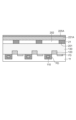
図5は、本実施形態に係る光電変換装置1のうちの1つの単位画素25に対応する断面図の一例である。
FIG. 5 is an example of a cross-sectional view corresponding to one
本実施形態に係る光電変換装置1は、図5に示すように、第1基板10と第2基板20と第3基板30を有する。なお、第1基板10と第2基板20と第3基板30は順に積層される。
The
第1基板10は第1半導体部材11と第1絶縁膜130を有する。第1半導体部材11は、光電変換素子PDと浮遊拡散部FDが配置される。ここで、光電変換素子PDはN型の半導体領域110を含む。また、第1絶縁膜130に転送トランジスタTRのゲート120が配置される。
The
第2基板20は第2半導体部材21と第2絶縁膜230を有する。第2半導体部材21に、画素トランジスタの第1ソース/ドレイン領域211が配置される。また、第2絶縁膜230に、画素トランジスタの第1ゲート220と配線構造体240、250が配置される。さらに、第2半導体部材21は素子分離領域201が配置されうる。
The
第3基板30は第3半導体部材31と第3絶縁膜310を有する。第3半導体部材31に、ゲートを含むMOSトランジスタなど、が設けられており、AD変換回路部や電流源40などの所定の信号処理部が配置されうる。また、第3絶縁膜310に、配線構造体320、350が配置される。
The
第1基板10と第2基板20と第3基板30は、第1絶縁膜130と第2半導体部材21と第2絶縁膜230と第3絶縁膜310の内部に配置された配線構造体240、250、320、350によりそれぞれ電気的に接続されうる。また、配線構造体250と配線構造体350及び、第2絶縁膜230と第3絶縁膜310はそれぞれ向き合うように積層されており、配線構造体250と配線構造体350とが電気的に接続されている。なお、第2基板20の深さ位置を貫通する配線構造体240は浮遊拡散部FDに電気的に接続する。さらに、配線構造体240は、第1ゲート220に電気的に接続する。
The
なお、第1半導体部材11は第1面140と第2面150を有し、第1面140が受光面となる。第1半導体部材11、第1絶縁膜130、第2半導体部材21、第2絶縁膜230、第3絶縁膜310、第3半導体部材31は第1面140側から第2面150側へ向かう方向に順番に積層される。
Note that the
また、第1半導体部材11の上には、第1面140側から順番に、層内レンズ、カラーフィルタ層、マイクロレンズなどの光学構造体(不図示)が配置されうる。
Furthermore, optical structures (not shown) such as an intralayer lens, a color filter layer, and a microlens may be arranged on the
以上に示すように、本実施形態に係る光電変換装置は、積層型センサであり、裏面照射型のセンサでもある。 As described above, the photoelectric conversion device according to this embodiment is a stacked sensor and also a back-illuminated sensor.
次に、本実施形態に係る光電変換装置の製造方法について、図6から図11を用いて説明する。図6から図11は、本実施形態に係る光電変換装置の製造方法を示す工程断面図の一例である。 Next, a method for manufacturing a photoelectric conversion device according to this embodiment will be described using FIGS. 6 to 11. 6 to 11 are examples of process cross-sectional views showing the method for manufacturing the photoelectric conversion device according to this embodiment.
まず、図6に示すように、第1半導体部材11に、光電変換素子PD及び浮遊拡散部FDが形成される。また、素子分離領域(不図示)も第1半導体部材11に形成され得る。ここで、光電変換素子PDの内部にN型の半導体領域110が形成される。また、浮遊拡散部FDはN型の半導体領域を含む。また、第2面150の上に、転送トランジスタTRのゲート120が形成される。ここで、ゲート120はN型のポリシリコンにより形成される。ここで、N型のポリシリコンは例えば減圧CVD法を用いて、成膜中にドーパントのガスを導入することで形成することが可能である。また、ポリシリコン膜形成後にイオン注入法を用いてN型の不純物を注入することで形成することも可能である。その後、第1絶縁膜130が第2面150の上に形成される。なお、第1半導体部材11は、例えばシリコン基板である。
First, as shown in FIG. 6, a photoelectric conversion element PD and a floating diffusion portion FD are formed in the
次に図7に示すように、第1絶縁膜130の上に第2半導体部材21を配する。ここで、例えば第1半導体部材11と第2半導体部材21はシリコン酸化膜である第1絶縁膜130を介して接合することが可能である。
Next, as shown in FIG. 7, the
その後、図8に示すように、第2半導体部材21が薄膜化される。また、第2半導体部材21に、素子分離領域201および第1ウェル領域202が形成される。ここで、第1ウェル領域202は素子分離領域201により電気的に分離されている。なお、第1ウェル領域202はN型の半導体領域を含む。
Thereafter, as shown in FIG. 8, the
その後、第2半導体部材21の上に画素トランジスタのゲート形成用にP型の第1ポリシリコン層220Aが形成される。ここで、P型のポリシリコンは例えば減圧CVD法を用いて、成膜中にドーパントのガスを導入することで形成することが可能である。また、ポリシリコン膜形成後にイオン注入法を用いてP型の不純物を注入することで形成することも可能である。
Thereafter, a P-type
ついで、図9に示すように、フォトリソグラフィ技術及び、エッチング技術を用いてトランジスタの第1ゲート220を第2半導体部材21の上に形成する。そして、第1ゲート220を形成した後に、イオン注入技術を用いて、P型の第1ソース/ドレイン領域211を第2半導体部材21に形成する。これによりP型のポリシリコンを含む第1ゲート220を有したP型の画素トランジスタが形成される。すなわち、第1半導体部材11に形成された光電変換素子PD及び浮遊拡散部FDを駆動するための、リセットトランジスタM2、増幅トランジスタM3、選択トランジスタM4、FD容量切り替えトランジスタM5等が、第2半導体部材21に形成される。
Next, as shown in FIG. 9, the
また、画素トランジスタを形成した後に、図10に示すように第2半導体部材21の上に第2絶縁膜230が形成される。その後、第2絶縁膜230の内部に配線構造体240、250が形成される。なお、配線構造体240は、第2基板20の深さ位置を貫通するように形成される。また、配線構造体240は浮遊拡散部FDと第1ゲート220に電気的に接続する。すなわち、第1半導体部材11と第2半導体部材21は配線構造体240により電気的に接続される。
Further, after forming the pixel transistor, a second
ここで、第2半導体部材21に形成された画素トランジスタは、第1半導体部材11と第2半導体部材21を積層した後に形成する方法に限るものではない。前もって第2半導体部材21に画素トランジスタを形成した後に、第1半導体部材11と第2半導体部材21を接合することも可能である。なお、図10に示す構造を第1基板10と第2基板20を備える積層体としてもよい。
Here, the pixel transistor formed in the
その後、図11に示すように、第3半導体部材31に第3絶縁膜310と配線構造体320、350が形成された第3基板30が第2基板20に積層される。すなわち、第1基板10と第2基板20を備える積層体に第3基板30が積層される。配線構造体250と配線構造体350及び、第2絶縁膜230と第3絶縁膜310がそれぞれ向き合うように、第2基板20と第3基板30は積層されており、配線構造体250と配線構造体350とが電気的に接続されている。ここで、例えば、配線構造体250、350はCuを主体とする導電性材料を含み、第2絶縁膜230、第3絶縁膜310はシリコン酸化膜を含む。それによって、Cu-Cuの金属接合及びシリコン酸化膜の共有結合により、第2基板20と第3基板30を接合することができる。ここで、第2絶縁膜230及び、第3絶縁膜310はシリコン酸化膜に限ったものではなく、複数の膜から構成することも可能である。
Thereafter, as shown in FIG. 11, a
また、第2基板20と第3基板30の積層方法はCu-Cuの金属接合とシリコン酸化膜の共有結合に限ったものではなく、絶縁膜同士の接合とすることも可能である。
Furthermore, the method of laminating the
また、第2基板20と第3基板30を積層した後に、第1半導体部材11を薄膜化する。なお、その後に、第1面140上に層内レンズ、カラーフィルタ層、マイクロレンズなどの光学構造体を形成してもよい。
Moreover, after the
このように、本実施形態に係る光電変換装置1は、光電変換素子PDがN型の半導体領域110を備え、読み出し回路22に含まれる画素トランジスタはPMOSで形成される。同一の基板上に導電型の異なるMOSトランジスタを形成する場合は、それぞれの導電型のトランジスタのウェル領域を電気的に分離するための物理的なスペースが必要になり、微細化しにくい構成となる。
As described above, in the
しかしながら、図5の構成の場合は、画素12と読み出し回路22に含まれる画素トランジスタが物理的に切り離された異なる基板上にそれぞれ形成される。そのため、当該2つの要素(画素12と画素トランジスタ)のウェル領域について、構造上、新たに分離のためにスペースを設ける必要がない。すなわち、光電変換素子PDを電子蓄積型フォトダイオードで形成する場合は、画素トランジスタをPMOSで形成したとしても、NMOSの場合に比べて、レイアウト効率の低減は生じにくい。
However, in the case of the configuration shown in FIG. 5, the pixel transistors included in the
さらに、同一の基板上に導電型の異なるMOSトランジスタを形成する場合は、MOSトランジスタ形成時にマスクの切り替えが必要となる。しかし、各基板上に単一の導電型のMOSトランジスタのみ形成し、各基板を積層する場合は、MOSトランジスタ形成時にマスクの切り替えは不要となる。 Furthermore, when forming MOS transistors of different conductivity types on the same substrate, it is necessary to switch masks when forming the MOS transistors. However, if only MOS transistors of a single conductivity type are formed on each substrate and the substrates are stacked, switching of masks is not necessary when forming the MOS transistors.
したがって、本実施形態によれば、電子蓄積型の光電変換素子を第1基板に形成し、増幅トランジスタを第2基板にPMOSで形成する。そうすることによって、高速駆動であり画素の1/fノイズを効果的に抑制し得る、微細化に適した光電変換装置を提供することが可能となる。 Therefore, according to this embodiment, the electron storage type photoelectric conversion element is formed on the first substrate, and the amplification transistor is formed on the second substrate using PMOS. By doing so, it becomes possible to provide a photoelectric conversion device suitable for miniaturization that can be driven at high speed and can effectively suppress 1/f noise of pixels.
〈第2実施形態〉
本発明による第2実施形態に係る光電変換装置1の構成について、図12と図13を用いて説明する。図12と図13は、本実施形態に係る光電変換装置1の製造方法を示す工程断面図の一例である。なお、第1実施形態と同様の構成要素には同一の符号が付されており、これらの構成要素についての説明は省略又は簡略化されることがある。
<Second embodiment>
The configuration of a
本実施形態は、PMOSのゲートの導電型が第1実施形態とは異なる。第1実施形態では、読み出し回路22に含まれる画素トランジスタのゲートがP型ポリシリコンで形成される例を挙げた。しかし、本実施形態では、画素トランジスタのゲートがN型ポリシリコンで形成される例について説明する。なお、本実施形態における光電変換装置1の概略構成を示す図1、画素12及び読み出し回路22の一例を示す図2から図4、概略断面を示す図5から図7は、第1実施形態と同様である。
This embodiment is different from the first embodiment in the conductivity type of the PMOS gate. In the first embodiment, an example was given in which the gate of the pixel transistor included in the
以下、本実施形態の読み出し回路22に含まれる画素トランジスタのゲートをN型ポリシリコンで形成する光電変換装置1の製造方法について説明する。なお、第2半導体部材21を積層するまでの工程は第1実施形態と同様であるため、説明は省略する。
A method for manufacturing the
図12に示すように、第2半導体部材21に素子分離領域201および第1ウェル領域202が形成される。ここで、第1ウェル領域202はN型の半導体領域を含む。その後、第2ポリシリコン層221AはN型のポリシリコンにより第2半導体部材21の上に形成される。ここで、N型のポリシリコンは例えば減圧CVD法を用いて、成膜中にドーパントのガスを導入することで形成することが可能である。また、ポリシリコン膜形成後にイオン注入法を用いてN型の不純物を注入することで形成することも可能である。次に、第2ポリシリコン層221A上にゲートのパターニング時にマスクとして機能するハードマスク層225Aが形成される。
As shown in FIG. 12, an
次に、図13に示すように、フォトリソグラフィ技術及び、エッチング技術を用いて、第2ゲート221、及びゲート上にハードマスク層225を形成する。その後、イオン注入技術を用いて、P型の第1ソース/ドレイン領域211が形成される。この際、ハードマスク層225がソース/ドレイン注入時にマスクとなり、第2ゲート221にP型の不純物が注入されることを抑制する。これにより低抵抗なN型のポリシリコンゲートを有したP型のトランジスタを形成することが可能となる。ここで、P型の第1ソース/ドレイン領域211を形成するために実施するイオン注入時のP型不純物濃度を、第2ゲート221中のN型不純物濃度より相対的に低くする。そうすることによって、ハードマスク層225を用いずにN型のゲートを有するP型トランジスタを形成することも可能である。
Next, as shown in FIG. 13, a
以上より、本実施形態によれば、電子蓄積型の光電変換素子を第1基板に形成し、増幅トランジスタを第2基板にPMOSで形成する。そうすることによって、高速駆動であり画素の1/fノイズを効果的に抑制し得る、微細化に適した光電変換装置を提供することが可能となる。 As described above, according to this embodiment, the electron storage type photoelectric conversion element is formed on the first substrate, and the amplification transistor is formed on the second substrate using PMOS. By doing so, it becomes possible to provide a photoelectric conversion device suitable for miniaturization that can be driven at high speed and can effectively suppress 1/f noise of pixels.
なお、ゲートのポリシリコンの導電型は、絶縁膜を介して対向する半導体基板との仕事関数差によって、当該ゲートを含むMOSトランジスタのしきい値電圧を決定するパラメータになり得る。読み出し回路22に含まれる画素トランジスタのゲートのポリシリコンの導電型を適宜設定することで、ゲートに印加される電圧幅が限られた条件においても、効果的にしきい値電圧を制御することが可能になる。
Note that the conductivity type of the polysilicon of the gate can be a parameter that determines the threshold voltage of the MOS transistor including the gate, depending on the work function difference between the polysilicon and the semiconductor substrate that faces the polysilicon through the insulating film. By appropriately setting the conductivity type of the polysilicon of the gate of the pixel transistor included in the
〈第3実施形態〉
本発明による第3実施形態に係る光電変換装置1の構成について、図14から図18を用いて説明する。なお、第1実施形態乃至第2実施形態と同様の構成要素には同一の符号が付されており、これらの構成要素についての説明は省略又は簡略化されることがある。
<Third embodiment>
The configuration of a
本実施形態は、画素トランジスタの導電型が第1実施形態乃至第2実施形態とは異なる。第1実施形態乃至第2実施形態では、画素トランジスタが全てPMOSで構成される例を挙げた。しかし、本実施形態では、画素トランジスタがNMOSとPMOSの2つの異なる導電型のMOSトランジスタを含む例について説明する。なお、光電変換装置1の概略構成を示す図1、概略断面を示す図5から図7は、第1実施形態乃至第2実施形態と同様である。しかし、単位画素25の回路構成は、第1実施形態及び第2実施形態とは異なる。
This embodiment is different from the first and second embodiments in the conductivity type of the pixel transistor. In the first embodiment and the second embodiment, an example was given in which all pixel transistors are composed of PMOS. However, in this embodiment, an example will be described in which the pixel transistor includes MOS transistors of two different conductivity types, NMOS and PMOS. Note that FIG. 1 showing a schematic configuration of the
図14から図16は、本実施形態に係る画素12及び読み出し回路22の回路図の一例である。ここでは、読み出し回路22に含まれるMOSトランジスタにおいて、リセットトランジスタM2及びFD容量切り替えトランジスタM5がNMOSで形成され、増幅トランジスタM3及び選択トランジスタM4がPMOSで形成される場合を例に挙げて説明する。この例は、リセットトランジスタM2及びFD容量切り替えトランジスタM5を画素12に含まれる転送トランジスタTRと同様の導電型で形成することができる。さらに、1/fやRTSノイズの低減に効果的なPMOSを増幅トランジスタM3に適用することができ、微細化及び読み出し回路22の低ノイズ化に効果的な構成であり得る。
14 to 16 are examples of circuit diagrams of the
なお、読み出し回路22に含まれる画素トランジスタの導電型の組み合わせについては、ここで説明する例に限定されるものではない。
Note that the combination of conductivity types of pixel transistors included in the
また、図14は、1つの画素12が1つの読み出し回路22に対応している場合の回路図である。本実施形形態においても、1つの読み出し回路22に接続される画素12の数は任意の数に変更可能である。より具体的に、2つの画素12が1つの読み出し回路22を共有している場合を図15に、4つの画素12が1つの読み出し回路22を共有している場合を図16に示す。ここで、「共有」とは、複数の画素12の出力が共通の読み出し回路22に入力されることを指している。
Further, FIG. 14 is a circuit diagram when one
なお、図14から図16に示される各画素12は、互いに共通の構成要素を有している。そのため、各画素12の構成要素を互いに区別するために、各画素12の構成要素の符号の末尾に識別番号(1,2,3,4)が付与されている。
Note that each
以下、本実施形態の読み出し回路22にNMOSとPMOSの2つの異なる導電型のMOSトランジスタが含まれる光電変換装置1の製造方法について説明する。図17と図18は、本実施形態に係る光電変換装置1の製造方法を示す工程断面図の一例である。なお、半導体部材21を積層するまでの工程は第1実施形態と同様であるため、説明は省略する。
Hereinafter, a method for manufacturing the
図17に示すように、第2半導体部材21に素子分離領域201と第2ウェル領域203と第3ウェル領域204が形成される。ここで、第2ウェル領域203と第3ウェル領域204はそれぞれ異なる極性を持つ半導体領域を含む。また、第3ポリシリコン層222Aと第4ポリシリコン層223Aはそれぞれ任意の導電型のポリシリコン層とすることが可能である。ここで、ポリシリコンは例えば減圧CVD法を用いて形成することが可能である。ポリシリコン膜形成後にフォトリソグラフィ技術により、任意の領域にイオン注入法を用いて不純物を注入することにより、N型、P型それぞれのポリシリコン層を形成することが可能である。次に、第3ポリシリコン層222Aと第4ポリシリコン層223Aの上にゲートのパターニング時のマスクとして機能するハードマスク層225Aが形成される。
As shown in FIG. 17, an
次に、図18に示すように、フォトリソグラフィ技術及び、エッチング技術を用いて、第3ゲート222、第4ゲート223及びそれぞれのゲート上にハードマスク層225を形成する。その後、イオン注入技術を用いて、第2ウェル領域203と異なる極性を持つ、第2ソース/ドレイン領域212を形成する。また、第3ウェル領域204と異なる極性を持つ、第3ソース/ドレイン領域213を同様に形成する。この際に、ハードマスク層225がソース/ドレイン注入時にマスクとなり、第3ゲート222と第4ゲート223にゲートと異なる極性を持つ不純物が注入されることを抑制する。これにより低抵抗なポリシリコンゲートを有したトランジスタを形成することが可能となる。ここで、任意の導電型の第2ソース/ドレイン領域212を形成するために実施するイオン注入時の不純物濃度を、第3ゲート222中の第2ソース/ドレイン領域とは異なる導電型の不純物濃度より相対的に低くする。そうすることによって、ハードマスク層225を用いずに任意の極性をもつゲートを有するトランジスタを形成することも可能である。
Next, as shown in FIG. 18, a
例えば、本実施形態の場合において、NMOSで形成されるリセットトランジスタM2及びFD容量切り替えトランジスタM5のゲートをN型のポリシリコンで形成する。さらに、PMOSで形成される増幅トランジスタM3及び選択トランジスタM4のゲートをP型のポリシリコンで形成する構成が考えられ得る。 For example, in the case of this embodiment, the gates of the reset transistor M2 and the FD capacitance switching transistor M5 formed of NMOS are formed of N-type polysilicon. Furthermore, a configuration may be considered in which the gates of the amplification transistor M3 and the selection transistor M4 formed of PMOS are formed of P-type polysilicon.
この後の工程については、第1の実施形態と同様であるため、説明を省略する。 The subsequent steps are the same as those in the first embodiment, so their explanation will be omitted.
以上より、本実施形態によれば、電子蓄積型の光電変換素子を第1基板に形成し、増幅トランジスタを第2基板にPMOSで形成する。そうすることによって、高速駆動であり画素の1/fノイズを効果的に抑制し得る、微細化に適した光電変換装置を提供することが可能となる。 As described above, according to this embodiment, the electron storage type photoelectric conversion element is formed on the first substrate, and the amplification transistor is formed on the second substrate using PMOS. By doing so, it becomes possible to provide a photoelectric conversion device suitable for miniaturization that can be driven at high speed and can effectively suppress 1/f noise of pixels.
〈第4実施形態〉
第4実施形態は第1実施形態乃至第3実施形態のいずれにも適用可能である。図19(a)は本実施形態の半導体装置930を備えた機器9191を説明する模式図である。半導体装置930には上記した各実施形態の光電変換装置を用いることができる。半導体装置930を備える機器9191について詳細に説明する。半導体装置930は、半導体デバイス910のほかに、半導体デバイス910を収容するパッケージ920を含むことができる。パッケージ920は、半導体デバイス910が固定された基体と、半導体デバイス910に対向するガラスなどの蓋体と、を含むことができる。パッケージ920は、さらに、基体に設けられた端子と半導体デバイス910に設けられた端子とを接続するボンディングワイヤやバンプなどの接合部材を含むことができる。
<Fourth embodiment>
The fourth embodiment is applicable to any of the first to third embodiments. FIG. 19A is a schematic diagram illustrating a
機器9191は、光学装置940、制御装置950、処理装置960、表示装置970、記憶装置980、機械装置990の少なくともいずれかを備えることができる。光学装置940は、半導体装置930に対応する。光学装置940は、例えばレンズやシャッター、ミラーである。制御装置950は、半導体装置930を制御する。制御装置950は、例えばASICなどの半導体装置である。
The
処理装置960は、半導体装置930から出力された信号を処理する。処理装置960は、AFE(アナログフロントエンド)あるいはDFE(デジタルフロントエンド)を構成するための、CPUやASICなどの半導体装置である。表示装置970は、半導体装置930で得られた情報(画像)を表示する、EL表示装置や液晶表示装置である。記憶装置980は、半導体装置930で得られた情報(画像)を記憶する、磁気デバイスや半導体デバイスである。記憶装置980は、SRAMやDRAMなどの揮発性メモリ、あるいは、フラッシュメモリやハードディスクドライブなどの不揮発性メモリである。
機械装置990は、モーターやエンジンなどの可動部あるいは推進部を有する。機器9191では、半導体装置930から出力された信号を表示装置970に表示したり、機器9191が備える通信装置(不図示)によって外部に送信したりする。そのために、機器9191は、半導体装置930が有する記憶回路や演算回路とは別に、記憶装置980や処理装置960をさらに備えることが好ましい。機械装置990は、半導体装置930から出力され信号に基づいて制御されてもよい。
また、機器9191は、撮影機能を有する情報端末(例えばスマートフォンやウエアラブル端末)やカメラ(例えばレンズ交換式カメラ、コンパクトカメラ、ビデオカメラ、監視カメラ)などの電子機器に適する。カメラにおける機械装置990はズーミングや合焦、シャッター動作のために光学装置940の部品を駆動することができる。あるいは、カメラにおける機械装置990は防振動作のために半導体装置930を移動することができる。
Further, the
また、機器9191は、車両や船舶、飛行体などの輸送機器であり得る。輸送機器における機械装置990は移動装置として用いられうる。輸送機器としての機器9191は、半導体装置930を輸送するものや、撮影機能により運転(操縦)の補助および/または自動化を行うものに好適である。運転(操縦)の補助および/または自動化のための処理装置960は、半導体装置930で得られた情報に基づいて移動装置としての機械装置990を操作するための処理を行うことができる。あるいは、機器9191は内視鏡などの医療機器や、測距センサなどの計測機器、電子顕微鏡のような分析機器、複写機などの事務機器、ロボットなどの産業機器であってもよい。
Further, the
上述した実施形態によれば、良好な画素特性を得ることが可能となる。従って、半導体装置の価値を高めることができる。ここでいう価値を高めることには、機能の追加、性能の向上、特性の向上、信頼性の向上、製造歩留まりの向上、環境負荷の低減、コストダウン、小型化、軽量化の少なくともいずれかが該当する。 According to the embodiments described above, it is possible to obtain good pixel characteristics. Therefore, the value of the semiconductor device can be increased. Increasing value here includes at least one of the following: adding functionality, improving performance, improving characteristics, improving reliability, improving manufacturing yield, reducing environmental impact, reducing cost, downsizing, and reducing weight. Applicable.
従って、本実施形態に係る半導体装置930を機器9191に用いれば、機器の価値をも向上することができる。例えば、半導体装置930を輸送機器に搭載して、輸送機器の外部の撮影や外部環境の測定を行う際に優れた性能を得ることができる。よって、輸送機器の製造、販売を行う上で、本実施形態に係る半導体装置を輸送機器へ搭載することを決定することは、輸送機器自体の性能を高める上で有利である。特に、半導体装置で得られた情報を用いて輸送機器の運転支援および/または自動運転を行う輸送機器に半導体装置930は好適である。
Therefore, if the
また、本実施形態の光電変換システム及び移動体について、図19(b)、(c)を用いて説明する。 Further, the photoelectric conversion system and moving body of this embodiment will be explained using FIGS. 19(b) and 19(c).
図19(a)は、車載カメラに関する光電変換システムの一例を示したものである。光電変換システム8は、光電変換装置1を有する。光電変換装置1は、上記のいずれかの実施形態に記載の光電変換装置(撮像装置)である。光電変換システム8は、光電変換装置1により取得された複数の画像データに対し、画像処理を行う画像処理部801と、光電変換システム8により取得された複数の画像データから視差(視差画像の位相差)の算出を行う視差取得部802を有する。また、光電変換システム8は、算出された視差に基づいて対象物までの距離を算出する距離取得部803と、算出された距離に基づいて衝突可能性があるか否かを判定する衝突判定部804と、を有する。ここで、視差取得部802や距離取得部803は、対象物までの距離情報を取得する距離情報取得手段の一例である。すなわち、距離情報とは、視差、デフォーカス量、対象物までの距離等に関する情報である。衝突判定部804はこれらの距離情報のいずれかを用いて、衝突可能性を判定してもよい。距離情報取得手段は、専用に設計されたハードウェアによって実現されてもよいし、ソフトウェアモジュールによって実現されてもよい。また、FPGA(Field Programmable Gate Array)やASIC(Application Specific Integrated Circuit)等によって実現されてもよいし、これらの組合せによって実現されてもよい。
FIG. 19(a) shows an example of a photoelectric conversion system related to an on-vehicle camera. The
光電変換システム8は車両情報取得装置810と接続されており、車速、ヨーレート、舵角などの車両情報を取得することができる。また、光電変換システム8は、衝突判定部804での判定結果に基づいて、車両に対して制動力を発生させる制御信号を出力する制御装置である制御ECU820が接続されている。また、光電変換システム8は、衝突判定部804での判定結果に基づいて、ドライバーへ警報を発する警報装置830とも接続されている。例えば、衝突判定部804の判定結果として衝突可能性が高い場合、制御ECU820はブレーキをかける、アクセルを戻す、エンジン出力を抑制するなどして衝突を回避、被害を軽減する車両制御を行う。警報装置830は音等の警報を鳴らす、カーナビゲーションシステムなどの画面に警報情報を表示する、シートベルトやステアリングに振動を与えるなどしてユーザに警告を行う。
The
本実施形態では、車両の周囲、例えば前方又は後方を光電変換システム8で撮像する。図19(c)に、車両前方(撮像範囲850)を撮像する場合の光電変換システムを示した。車両情報取得装置810が、光電変換システム8ないしは光電変換装置1に指示を送る。このような構成により、測距の精度をより向上させることができる。
In this embodiment, the
上記では、他の車両と衝突しないように制御する例を説明したが、他の車両に追従して自動運転する制御や、車線からはみ出さないように自動運転する制御などにも適用可能である。更に、光電変換システムは、自車両等の車両に限らず、例えば、船舶、航空機あるいは産業用ロボットなどの移動体(移動装置)に適用することができる。加えて、移動体に限らず、高度道路交通システム(ITS)等、広く物体認識を利用する機器に適用することができる。 Above, we explained an example of control to avoid collisions with other vehicles, but it can also be applied to control to automatically drive while following other vehicles, control to automatically drive to avoid moving out of the lane, etc. . Furthermore, the photoelectric conversion system can be applied not only to vehicles such as own vehicles, but also to mobile objects (mobile devices) such as ships, aircraft, and industrial robots. In addition, the present invention can be applied not only to mobile objects but also to a wide range of devices that use object recognition, such as intelligent transportation systems (ITS).
以上、説明した実施形態は、技術思想を逸脱しない範囲において適宜変更が可能である。なお、本明細書の開示内容は、本明細書に記載したことのみならず、本明細書および本明細書に添付した図面から把握可能な全ての事項を含む。また本明細書の開示内容は、本明細書に記載した概念の補集合を含んでいる。すなわち、本明細書に例えば「AはBよりも大きい」旨の記載があれば、「AはBよりも大きくない」旨の記載を省略しても、本明細書は「AはBよりも大きくない」旨を開示していると云える。なぜなら、「AはBよりも大きい」旨を記載している場合には、「AはBよりも大きくない」場合を考慮していることが前提だからである。 The embodiments described above can be modified as appropriate without departing from the technical concept. Note that the disclosure content of this specification includes not only what is described in this specification, but also all matters that can be understood from this specification and the drawings attached to this specification. The disclosure herein also includes the complement of the concepts described herein. In other words, if the specification includes, for example, the statement "A is greater than B", even if the statement "A is not greater than B" is omitted, the specification still states "A is greater than B". It can be said that the company has disclosed that it is not large. This is because when it is stated that "A is larger than B", it is assumed that "A is not larger than B" is being considered.
なお、本実施形態の開示は、以下の構成および方法を含む。 Note that the disclosure of this embodiment includes the following configuration and method.
(構成1)光電変換素子を有する第1基板と、前記光電変換素子から出力される信号電荷である電子を増幅する増幅トランジスタを有する第2基板と、を備える光電変換装置であって、前記光電変換素子は前記電子を蓄積するN型の半導体領域を備え、前記増幅トランジスタはP型のMOSトランジスタであることを特徴とする光電変換装置。 (Structure 1) A photoelectric conversion device comprising a first substrate having a photoelectric conversion element and a second substrate having an amplification transistor that amplifies electrons that are signal charges output from the photoelectric conversion element, the photoelectric conversion device comprising: A photoelectric conversion device characterized in that the conversion element includes an N-type semiconductor region that accumulates the electrons, and the amplification transistor is a P-type MOS transistor.
(構成2)前記第1基板は前記電子を前記増幅トランジスタに転送する転送トランジスタを有し、前記転送トランジスタはN型のMOSトランジスタであることを特徴とする構成1に記載の光電変換装置。
(Structure 2) The photoelectric conversion device according to
(構成3)前記第2基板は、リセットトランジスタと選択トランジスタとFD容量切り替えトランジスタを有し、前記リセットトランジスタと前記選択トランジスタと前記FD容量切り替えトランジスタはP型のMOSトランジスタであることを特徴とする構成1または2に記載の光電変換装置。
(Structure 3) The second substrate has a reset transistor, a selection transistor, and an FD capacitance switching transistor, and the reset transistor, the selection transistor, and the FD capacitance switching transistor are P-type MOS transistors. The photoelectric conversion device according to
(構成4)前記増幅トランジスタのゲートは、P型のポリシリコンにより形成されていることを特徴とする構成1乃至3のいずれか1項に記載の光電変換装置。
(Structure 4) The photoelectric conversion device according to any one of
(構成5)前記増幅トランジスタのゲートは、N型のポリシリコンにより形成されていることを特徴とする構成1乃至3のいずれか1項に記載の光電変換装置。
(Structure 5) The photoelectric conversion device according to any one of
(構成6)前記第2基板はリセットトランジスタと選択トランジスタとFD容量切り替えトランジスタを有し、前記選択トランジスタはP型のMOSトランジスタであり、前記リセットトランジスタとFD容量切り替えトランジスタはN型のMOSトランジスタであることを特徴とする構成1または2または4または5のいずれか1項に記載の光電変換装置。
(Configuration 6) The second substrate has a reset transistor, a selection transistor, and an FD capacitance switching transistor, the selection transistor is a P-type MOS transistor, and the reset transistor and the FD capacitance switching transistor are N-type MOS transistors. The photoelectric conversion device according to any one of
(構成7)前記第2基板は前記第1基板に積層されることを特徴とする構成1乃至6のいずれか1項に記載の光電変換装置。
(Structure 7) The photoelectric conversion device according to any one of
(構成8)前記増幅トランジスタから出力される画素信号を処理するロジック回路を有する第3基板を備えることを特徴とする構成1乃至7のいずれか1項に記載の光電変換装置。
(Structure 8) The photoelectric conversion device according to any one of
(構成9)前記第2基板は、リセットトランジスタを有し、前記リセットトランジスタに供給される第1電源電圧と前記増幅トランジスタに供給される第2電源電圧とが異なることを特徴とする構成1乃至8のいずれか1項に記載の光電変換装置。 (Structure 9) The second substrate has a reset transistor, and the first power supply voltage supplied to the reset transistor and the second power supply voltage supplied to the amplification transistor are different from each other. 8. The photoelectric conversion device according to any one of 8.
(構成10)前記第2基板は、リセットトランジスタを有し、前記リセットトランジスタに供給される第1電源電圧は、基準電圧より大きく、前記増幅トランジスタに供給される第2電源電圧より小さいことを特徴とする構成1乃至9のいずれか1項に記載の光電変換装置。
(Structure 10) The second substrate has a reset transistor, and the first power supply voltage supplied to the reset transistor is higher than a reference voltage and lower than the second power supply voltage supplied to the amplification transistor. The photoelectric conversion device according to any one of
(構成11)前記光電変換素子のアノードに負バイアスを印加することを特徴とする構成10に記載の光電変換装置。
(Structure 11) The photoelectric conversion device according to
(構成12)前記第3基板は前記第2基板に積層されることを特徴とする構成8に記載の光電変換装置。
(Structure 12) The photoelectric conversion device according to
(構成13)前記第1基板は浮遊拡散部を有し、前記第2基板の深さ位置を貫通する配線構造体が前記浮遊拡散部に電気的に接続することを特徴とする構成1乃至12のいずれか1項に記載の光電変換装置。
(Structure 13)
(構成14)前記配線構造体は、前記増幅トランジスタのゲートに電気的に接続することを特徴とする構成13に記載の光電変換装置。
(Structure 14) The photoelectric conversion device according to
(構成15)構成1乃至14のいずれか1項に記載の光電変換装置を備える機器であって、前記光電変換装置に対応した光学装置、前記光電変換装置を制御する制御装置、前記光電変換装置から出力された信号を処理する処理装置、前記光電変換装置で得られた情報を表示する表示装置、前記光電変換装置で得られた情報を記憶する記憶装置、および、前記光電変換装置で得られた情報に基づいて動作する機械装置、の少なくともいずれかを更に備えることを特徴とする機器。
(Configuration 15) A device comprising the photoelectric conversion device according to any one of
(構成16)光電変換素子を有する第1基板と、前記光電変換素子から出力される信号電荷である電子を増幅する増幅トランジスタを有する第2基板と、を備える積層体であって、前記光電変換素子は前記電子を蓄積するN型の半導体領域を備え、前記増幅トランジスタはP型のMOSトランジスタであることを特徴とする積層体。 (Structure 16) A laminate including a first substrate having a photoelectric conversion element and a second substrate having an amplification transistor that amplifies electrons that are signal charges output from the photoelectric conversion element, A stacked body characterized in that the element includes an N-type semiconductor region that stores the electrons, and the amplification transistor is a P-type MOS transistor.
(構成17)前記増幅トランジスタから出力される画素信号を処理するロジック回路を有する第3基板を備え、前記第3基板は前記第2基板に積層されることを特徴とする構成16に記載の積層体。 (Structure 17) The multilayer structure according to Structure 16, further comprising a third substrate having a logic circuit that processes a pixel signal output from the amplification transistor, and the third substrate is stacked on the second substrate. body.
10 第1基板
20 第2基板
110 N型の半導体領域
PD 光電変換素子
M3 増幅トランジスタ
10
Claims (17)
前記光電変換素子から出力される信号電荷である電子を増幅する増幅トランジスタを有する第2基板と、
を備える光電変換装置であって、
前記光電変換素子は前記電子を蓄積するN型の半導体領域を備え、
前記増幅トランジスタはP型のMOSトランジスタである
ことを特徴とする光電変換装置。 a first substrate having a photoelectric conversion element;
a second substrate having an amplification transistor that amplifies electrons that are signal charges output from the photoelectric conversion element;
A photoelectric conversion device comprising:
The photoelectric conversion element includes an N-type semiconductor region that accumulates the electrons,
A photoelectric conversion device characterized in that the amplification transistor is a P-type MOS transistor.
前記光電変換装置に対応した光学装置、
前記光電変換装置を制御する制御装置、
前記光電変換装置から出力された信号を処理する処理装置、
前記光電変換装置で得られた情報を表示する表示装置、
前記光電変換装置で得られた情報を記憶する記憶装置、および、
前記光電変換装置で得られた情報に基づいて動作する機械装置、の少なくともいずれかを更に備えることを特徴とする機器。 A device comprising the photoelectric conversion device according to any one of claims 1 to 14,
an optical device compatible with the photoelectric conversion device;
a control device that controls the photoelectric conversion device;
a processing device that processes the signal output from the photoelectric conversion device;
a display device that displays information obtained by the photoelectric conversion device;
a storage device that stores information obtained by the photoelectric conversion device; and
A device further comprising at least one of a mechanical device that operates based on information obtained by the photoelectric conversion device.
前記光電変換素子から出力される信号電荷である電子を増幅する増幅トランジスタを有する第2基板と、
を備える積層体であって、
前記光電変換素子は前記電子を蓄積するN型の半導体領域を備え、
前記増幅トランジスタはP型のMOSトランジスタである
ことを特徴とする積層体。 a first substrate having a photoelectric conversion element;
a second substrate having an amplification transistor that amplifies electrons that are signal charges output from the photoelectric conversion element;
A laminate comprising:
The photoelectric conversion element includes an N-type semiconductor region that accumulates the electrons,
A stacked body characterized in that the amplification transistor is a P-type MOS transistor.
Priority Applications (2)
| Application Number | Priority Date | Filing Date | Title |
|---|---|---|---|
| JP2022104633A JP2024004794A (en) | 2022-06-29 | 2022-06-29 | Photoelectric conversion device, apparatus, and laminate |
| US18/342,473 US20240006451A1 (en) | 2022-06-29 | 2023-06-27 | Photoelectric conversion apparatus, equipment, layered structure |
Applications Claiming Priority (1)
| Application Number | Priority Date | Filing Date | Title |
|---|---|---|---|
| JP2022104633A JP2024004794A (en) | 2022-06-29 | 2022-06-29 | Photoelectric conversion device, apparatus, and laminate |
Publications (1)
| Publication Number | Publication Date |
|---|---|
| JP2024004794A true JP2024004794A (en) | 2024-01-17 |
Family
ID=89432639
Family Applications (1)
| Application Number | Title | Priority Date | Filing Date |
|---|---|---|---|
| JP2022104633A Pending JP2024004794A (en) | 2022-06-29 | 2022-06-29 | Photoelectric conversion device, apparatus, and laminate |
Country Status (2)
| Country | Link |
|---|---|
| US (1) | US20240006451A1 (en) |
| JP (1) | JP2024004794A (en) |
-
2022
- 2022-06-29 JP JP2022104633A patent/JP2024004794A/en active Pending
-
2023
- 2023-06-27 US US18/342,473 patent/US20240006451A1/en active Pending
Also Published As
| Publication number | Publication date |
|---|---|
| US20240006451A1 (en) | 2024-01-04 |
Similar Documents
| Publication | Publication Date | Title |
|---|---|---|
| US20220285410A1 (en) | Semiconductor apparatus and device | |
| JP2019041352A (en) | Imaging apparatus and imaging system | |
| JP7154795B2 (en) | IMAGING DEVICE, IMAGING SYSTEM, AND MOVING OBJECT | |
| JP7214373B2 (en) | Solid-state imaging device, method for manufacturing solid-state imaging device, and imaging system | |
| JP2024004794A (en) | Photoelectric conversion device, apparatus, and laminate | |
| JP2020088293A (en) | Photoelectric conversion device, photoelectric conversion system, and moving body | |
| JP7341724B2 (en) | Photoelectric conversion device and photoelectric conversion system | |
| JP2023178690A (en) | Photoelectric conversion apparatus and equipment | |
| JP2021132095A (en) | Photoelectric conversion device, imaging system, mobile object | |
| US20230420468A1 (en) | Photoelectric conversion device | |
| JP2023178688A (en) | Photoelectric conversion apparatus and equipment | |
| US20240038811A1 (en) | Photoelectric conversion apparatus and equipment | |
| US20210280627A1 (en) | Semiconductor device and equipment | |
| US20240128285A1 (en) | Photoelectric conversion device and equipment | |
| US20230395622A1 (en) | Photoelectric conversion apparatus and equipment | |
| US20240136370A1 (en) | Photoelectric conversion apparatus, method of driving the apparatus, semiconductor substrate, and equipment | |
| US20240038816A1 (en) | Photoelectric conversion device and apparatus | |
| JP2020057689A (en) | Solid-state imaging device and manufacturing method thereof | |
| JP2023178689A (en) | Photoelectric conversion device and photoelectric conversion system | |
| JP2020088291A (en) | Photoelectric conversion device, photoelectric conversion system, and moving body | |
| US11616925B2 (en) | Photoelectric conversion apparatus and equipment | |
| JP2024058185A (en) | Photoelectric conversion device, driving method for photoelectric conversion device, semiconductor substrate, and device | |
| US20230038959A1 (en) | Photoelectric conversion device | |
| JP2024006956A (en) | Photoelectric conversion device, manufacturing method for photoelectric conversion device, apparatus | |
| US11728358B2 (en) | Photoelectric conversion apparatus, image sensor, semiconductor apparatus, photoelectric conversion system, and equipment |
Legal Events
| Date | Code | Title | Description |
|---|---|---|---|
| RD01 | Notification of change of attorney |
Free format text: JAPANESE INTERMEDIATE CODE: A7421 Effective date: 20221018 |
|
| RD01 | Notification of change of attorney |
Free format text: JAPANESE INTERMEDIATE CODE: A7421 Effective date: 20231213 |