JP2023099439A - Laminate-type electronic component - Google Patents
Laminate-type electronic component Download PDFInfo
- Publication number
- JP2023099439A JP2023099439A JP2022164651A JP2022164651A JP2023099439A JP 2023099439 A JP2023099439 A JP 2023099439A JP 2022164651 A JP2022164651 A JP 2022164651A JP 2022164651 A JP2022164651 A JP 2022164651A JP 2023099439 A JP2023099439 A JP 2023099439A
- Authority
- JP
- Japan
- Prior art keywords
- electronic component
- component according
- multilayer electronic
- electrode
- insulating layer
- Prior art date
- Legal status (The legal status is an assumption and is not a legal conclusion. Google has not performed a legal analysis and makes no representation as to the accuracy of the status listed.)
- Pending
Links
- 238000007747 plating Methods 0.000 claims abstract description 233
- 229910052735 hafnium Inorganic materials 0.000 claims abstract description 58
- VBJZVLUMGGDVMO-UHFFFAOYSA-N hafnium atom Chemical compound [Hf] VBJZVLUMGGDVMO-UHFFFAOYSA-N 0.000 claims abstract description 58
- 238000009413 insulation Methods 0.000 claims abstract description 22
- 229910052751 metal Inorganic materials 0.000 claims description 55
- 239000002184 metal Substances 0.000 claims description 55
- 239000011521 glass Substances 0.000 claims description 38
- PXHVJJICTQNCMI-UHFFFAOYSA-N nickel Substances [Ni] PXHVJJICTQNCMI-UHFFFAOYSA-N 0.000 claims description 36
- 238000000034 method Methods 0.000 claims description 35
- 229910052782 aluminium Inorganic materials 0.000 claims description 25
- XAGFODPZIPBFFR-UHFFFAOYSA-N aluminium Chemical compound [Al] XAGFODPZIPBFFR-UHFFFAOYSA-N 0.000 claims description 25
- 229910052759 nickel Inorganic materials 0.000 claims description 16
- 239000010949 copper Substances 0.000 claims description 13
- 229910045601 alloy Inorganic materials 0.000 claims description 10
- 239000000956 alloy Substances 0.000 claims description 10
- 229910052802 copper Inorganic materials 0.000 claims description 9
- CJNBYAVZURUTKZ-UHFFFAOYSA-N hafnium(IV) oxide Inorganic materials O=[Hf]=O CJNBYAVZURUTKZ-UHFFFAOYSA-N 0.000 claims description 9
- 229910000990 Ni alloy Inorganic materials 0.000 claims description 7
- 238000013459 approach Methods 0.000 claims description 7
- RYGMFSIKBFXOCR-UHFFFAOYSA-N Copper Chemical compound [Cu] RYGMFSIKBFXOCR-UHFFFAOYSA-N 0.000 claims description 4
- QVGXLLKOCUKJST-UHFFFAOYSA-N atomic oxygen Chemical compound [O] QVGXLLKOCUKJST-UHFFFAOYSA-N 0.000 claims 12
- 229910052760 oxygen Inorganic materials 0.000 claims 12
- 239000001301 oxygen Substances 0.000 claims 12
- PNEYBMLMFCGWSK-UHFFFAOYSA-N aluminium oxide Inorganic materials [O-2].[O-2].[O-2].[Al+3].[Al+3] PNEYBMLMFCGWSK-UHFFFAOYSA-N 0.000 claims 4
- 229910052593 corundum Inorganic materials 0.000 claims 4
- 229910001845 yogo sapphire Inorganic materials 0.000 claims 4
- 239000000463 material Substances 0.000 description 29
- 230000000694 effects Effects 0.000 description 27
- 230000035515 penetration Effects 0.000 description 20
- 230000008569 process Effects 0.000 description 20
- 239000000758 substrate Substances 0.000 description 17
- 239000011135 tin Substances 0.000 description 16
- 238000012986 modification Methods 0.000 description 13
- 230000004048 modification Effects 0.000 description 13
- 229910000679 solder Inorganic materials 0.000 description 13
- KDLHZDBZIXYQEI-UHFFFAOYSA-N Palladium Chemical compound [Pd] KDLHZDBZIXYQEI-UHFFFAOYSA-N 0.000 description 12
- 238000009792 diffusion process Methods 0.000 description 12
- 230000032798 delamination Effects 0.000 description 10
- 239000011347 resin Substances 0.000 description 10
- 229920005989 resin Polymers 0.000 description 10
- 238000010304 firing Methods 0.000 description 9
- 238000005520 cutting process Methods 0.000 description 8
- 229910052763 palladium Inorganic materials 0.000 description 8
- 229910052718 tin Inorganic materials 0.000 description 8
- 239000000919 ceramic Substances 0.000 description 7
- 239000003985 ceramic capacitor Substances 0.000 description 7
- 230000005855 radiation Effects 0.000 description 7
- 229910052709 silver Inorganic materials 0.000 description 7
- 239000010936 titanium Substances 0.000 description 7
- 125000004429 atom Chemical group 0.000 description 6
- 238000000231 atomic layer deposition Methods 0.000 description 6
- 239000010931 gold Substances 0.000 description 6
- 125000004430 oxygen atom Chemical group O* 0.000 description 6
- BASFCYQUMIYNBI-UHFFFAOYSA-N platinum Chemical compound [Pt] BASFCYQUMIYNBI-UHFFFAOYSA-N 0.000 description 6
- 230000008602 contraction Effects 0.000 description 5
- 238000007598 dipping method Methods 0.000 description 5
- 230000035699 permeability Effects 0.000 description 5
- 239000010944 silver (metal) Substances 0.000 description 5
- 239000000126 substance Substances 0.000 description 5
- XLYOFNOQVPJJNP-UHFFFAOYSA-N water Substances O XLYOFNOQVPJJNP-UHFFFAOYSA-N 0.000 description 5
- 229910002113 barium titanate Inorganic materials 0.000 description 4
- JRPBQTZRNDNNOP-UHFFFAOYSA-N barium titanate Chemical compound [Ba+2].[Ba+2].[O-][Ti]([O-])([O-])[O-] JRPBQTZRNDNNOP-UHFFFAOYSA-N 0.000 description 4
- 230000015572 biosynthetic process Effects 0.000 description 4
- 229910052737 gold Inorganic materials 0.000 description 4
- 238000005245 sintering Methods 0.000 description 4
- 238000012360 testing method Methods 0.000 description 4
- 239000004925 Acrylic resin Substances 0.000 description 3
- 229920000178 Acrylic resin Polymers 0.000 description 3
- 238000012935 Averaging Methods 0.000 description 3
- 239000001856 Ethyl cellulose Substances 0.000 description 3
- ZZSNKZQZMQGXPY-UHFFFAOYSA-N Ethyl cellulose Chemical compound CCOCC1OC(OC)C(OCC)C(OCC)C1OC1C(O)C(O)C(OC)C(CO)O1 ZZSNKZQZMQGXPY-UHFFFAOYSA-N 0.000 description 3
- 239000002253 acid Substances 0.000 description 3
- 229910052804 chromium Inorganic materials 0.000 description 3
- 239000011651 chromium Substances 0.000 description 3
- 239000003822 epoxy resin Substances 0.000 description 3
- -1 etc. may be included Substances 0.000 description 3
- 229920001249 ethyl cellulose Polymers 0.000 description 3
- 235000019325 ethyl cellulose Nutrition 0.000 description 3
- 239000010408 film Substances 0.000 description 3
- 230000014509 gene expression Effects 0.000 description 3
- 230000006872 improvement Effects 0.000 description 3
- 239000012535 impurity Substances 0.000 description 3
- 229920000647 polyepoxide Polymers 0.000 description 3
- 239000000843 powder Substances 0.000 description 3
- 238000007789 sealing Methods 0.000 description 3
- 239000010409 thin film Substances 0.000 description 3
- BQCADISMDOOEFD-UHFFFAOYSA-N Silver Chemical compound [Ag] BQCADISMDOOEFD-UHFFFAOYSA-N 0.000 description 2
- ATJFFYVFTNAWJD-UHFFFAOYSA-N Tin Chemical compound [Sn] ATJFFYVFTNAWJD-UHFFFAOYSA-N 0.000 description 2
- RTAQQCXQSZGOHL-UHFFFAOYSA-N Titanium Chemical compound [Ti] RTAQQCXQSZGOHL-UHFFFAOYSA-N 0.000 description 2
- 239000011230 binding agent Substances 0.000 description 2
- 230000000740 bleeding effect Effects 0.000 description 2
- 239000003990 capacitor Substances 0.000 description 2
- 229910010293 ceramic material Inorganic materials 0.000 description 2
- 230000007797 corrosion Effects 0.000 description 2
- 238000005260 corrosion Methods 0.000 description 2
- 230000007547 defect Effects 0.000 description 2
- 230000003628 erosive effect Effects 0.000 description 2
- 238000011156 evaluation Methods 0.000 description 2
- PCHJSUWPFVWCPO-UHFFFAOYSA-N gold Chemical compound [Au] PCHJSUWPFVWCPO-UHFFFAOYSA-N 0.000 description 2
- 239000007788 liquid Substances 0.000 description 2
- 238000004519 manufacturing process Methods 0.000 description 2
- 238000005259 measurement Methods 0.000 description 2
- 239000000203 mixture Substances 0.000 description 2
- 229910052697 platinum Inorganic materials 0.000 description 2
- 230000001902 propagating effect Effects 0.000 description 2
- 239000004332 silver Substances 0.000 description 2
- 229910052719 titanium Inorganic materials 0.000 description 2
- WFKWXMTUELFFGS-UHFFFAOYSA-N tungsten Chemical compound [W] WFKWXMTUELFFGS-UHFFFAOYSA-N 0.000 description 2
- 229910052721 tungsten Inorganic materials 0.000 description 2
- 239000010937 tungsten Substances 0.000 description 2
- 229910018072 Al 2 O 3 Inorganic materials 0.000 description 1
- 239000000654 additive Substances 0.000 description 1
- 239000000853 adhesive Substances 0.000 description 1
- 230000001070 adhesive effect Effects 0.000 description 1
- 238000005054 agglomeration Methods 0.000 description 1
- 230000002776 aggregation Effects 0.000 description 1
- 230000009286 beneficial effect Effects 0.000 description 1
- 230000000903 blocking effect Effects 0.000 description 1
- 239000002131 composite material Substances 0.000 description 1
- 230000002542 deteriorative effect Effects 0.000 description 1
- 238000007599 discharging Methods 0.000 description 1
- 239000002270 dispersing agent Substances 0.000 description 1
- 230000005611 electricity Effects 0.000 description 1
- 238000002149 energy-dispersive X-ray emission spectroscopy Methods 0.000 description 1
- 238000005516 engineering process Methods 0.000 description 1
- 230000005484 gravity Effects 0.000 description 1
- 238000007646 gravure printing Methods 0.000 description 1
- 239000011810 insulating material Substances 0.000 description 1
- 238000010030 laminating Methods 0.000 description 1
- 239000004973 liquid crystal related substance Substances 0.000 description 1
- 230000003287 optical effect Effects 0.000 description 1
- 239000003960 organic solvent Substances 0.000 description 1
- 239000012466 permeate Substances 0.000 description 1
- 238000005498 polishing Methods 0.000 description 1
- 229920001721 polyimide Polymers 0.000 description 1
- 238000007639 printing Methods 0.000 description 1
- 239000000047 product Substances 0.000 description 1
- 230000001681 protective effect Effects 0.000 description 1
- 239000002994 raw material Substances 0.000 description 1
- 238000007650 screen-printing Methods 0.000 description 1
- 239000004065 semiconductor Substances 0.000 description 1
- VEALVRVVWBQVSL-UHFFFAOYSA-N strontium titanate Chemical compound [Sr+2].[O-][Ti]([O-])=O VEALVRVVWBQVSL-UHFFFAOYSA-N 0.000 description 1
- 238000006467 substitution reaction Methods 0.000 description 1
- 238000002834 transmittance Methods 0.000 description 1
Images


Classifications
-
- H—ELECTRICITY
- H01—ELECTRIC ELEMENTS
- H01G—CAPACITORS; CAPACITORS, RECTIFIERS, DETECTORS, SWITCHING DEVICES OR LIGHT-SENSITIVE DEVICES, OF THE ELECTROLYTIC TYPE
- H01G4/00—Fixed capacitors; Processes of their manufacture
- H01G4/30—Stacked capacitors
-
- H—ELECTRICITY
- H01—ELECTRIC ELEMENTS
- H01G—CAPACITORS; CAPACITORS, RECTIFIERS, DETECTORS, SWITCHING DEVICES OR LIGHT-SENSITIVE DEVICES, OF THE ELECTROLYTIC TYPE
- H01G2/00—Details of capacitors not covered by a single one of groups H01G4/00-H01G11/00
- H01G2/02—Mountings
- H01G2/06—Mountings specially adapted for mounting on a printed-circuit support
- H01G2/065—Mountings specially adapted for mounting on a printed-circuit support for surface mounting, e.g. chip capacitors
-
- H—ELECTRICITY
- H01—ELECTRIC ELEMENTS
- H01G—CAPACITORS; CAPACITORS, RECTIFIERS, DETECTORS, SWITCHING DEVICES OR LIGHT-SENSITIVE DEVICES, OF THE ELECTROLYTIC TYPE
- H01G4/00—Fixed capacitors; Processes of their manufacture
- H01G4/002—Details
-
- H—ELECTRICITY
- H01—ELECTRIC ELEMENTS
- H01G—CAPACITORS; CAPACITORS, RECTIFIERS, DETECTORS, SWITCHING DEVICES OR LIGHT-SENSITIVE DEVICES, OF THE ELECTROLYTIC TYPE
- H01G4/00—Fixed capacitors; Processes of their manufacture
- H01G4/002—Details
- H01G4/005—Electrodes
- H01G4/008—Selection of materials
-
- H—ELECTRICITY
- H01—ELECTRIC ELEMENTS
- H01G—CAPACITORS; CAPACITORS, RECTIFIERS, DETECTORS, SWITCHING DEVICES OR LIGHT-SENSITIVE DEVICES, OF THE ELECTROLYTIC TYPE
- H01G4/00—Fixed capacitors; Processes of their manufacture
- H01G4/002—Details
- H01G4/005—Electrodes
- H01G4/012—Form of non-self-supporting electrodes
-
- H—ELECTRICITY
- H01—ELECTRIC ELEMENTS
- H01G—CAPACITORS; CAPACITORS, RECTIFIERS, DETECTORS, SWITCHING DEVICES OR LIGHT-SENSITIVE DEVICES, OF THE ELECTROLYTIC TYPE
- H01G4/00—Fixed capacitors; Processes of their manufacture
- H01G4/002—Details
- H01G4/224—Housing; Encapsulation
-
- H—ELECTRICITY
- H01—ELECTRIC ELEMENTS
- H01G—CAPACITORS; CAPACITORS, RECTIFIERS, DETECTORS, SWITCHING DEVICES OR LIGHT-SENSITIVE DEVICES, OF THE ELECTROLYTIC TYPE
- H01G4/00—Fixed capacitors; Processes of their manufacture
- H01G4/002—Details
- H01G4/228—Terminals
- H01G4/232—Terminals electrically connecting two or more layers of a stacked or rolled capacitor
- H01G4/2325—Terminals electrically connecting two or more layers of a stacked or rolled capacitor characterised by the material of the terminals
-
- H—ELECTRICITY
- H01—ELECTRIC ELEMENTS
- H01G—CAPACITORS; CAPACITORS, RECTIFIERS, DETECTORS, SWITCHING DEVICES OR LIGHT-SENSITIVE DEVICES, OF THE ELECTROLYTIC TYPE
- H01G4/00—Fixed capacitors; Processes of their manufacture
- H01G4/002—Details
- H01G4/018—Dielectrics
- H01G4/06—Solid dielectrics
- H01G4/08—Inorganic dielectrics
- H01G4/12—Ceramic dielectrics
- H01G4/1209—Ceramic dielectrics characterised by the ceramic dielectric material
-
- Y—GENERAL TAGGING OF NEW TECHNOLOGICAL DEVELOPMENTS; GENERAL TAGGING OF CROSS-SECTIONAL TECHNOLOGIES SPANNING OVER SEVERAL SECTIONS OF THE IPC; TECHNICAL SUBJECTS COVERED BY FORMER USPC CROSS-REFERENCE ART COLLECTIONS [XRACs] AND DIGESTS
- Y02—TECHNOLOGIES OR APPLICATIONS FOR MITIGATION OR ADAPTATION AGAINST CLIMATE CHANGE
- Y02E—REDUCTION OF GREENHOUSE GAS [GHG] EMISSIONS, RELATED TO ENERGY GENERATION, TRANSMISSION OR DISTRIBUTION
- Y02E60/00—Enabling technologies; Technologies with a potential or indirect contribution to GHG emissions mitigation
- Y02E60/13—Energy storage using capacitors
Abstract
Description
本発明は、積層型電子部品に関するものである。 The present invention relates to a multilayer electronic component.
積層型電子部品の一つである積層セラミックキャパシタ(MLCC:Multi-Layered Ceramic Capacitor)は、液晶表示装置(LCD:Liquid Crystal Display)及びプラズマ表示装置パネル(PDP:Plasma Display Panel)などの映像機器、コンピュータ、スマートフォン及び携帯電話など、様々な電子製品の印刷回路基板に装着され、電気を充電又は放電させる役割を果たすチップ型のコンデンサである。 A multi-layered ceramic capacitor (MLCC), which is one of laminated electronic components, is used in video equipment such as liquid crystal displays (LCDs) and plasma display panels (PDPs). It is a chip-type capacitor that is attached to the printed circuit board of various electronic products such as computers, smart phones, and mobile phones, and plays a role of charging or discharging electricity.
このような積層セラミックキャパシタは、小型でありながらも高容量が保障され、実装が容易であるという利点により、様々な電子装置の部品として使用されることができる。コンピュータ、モバイル機器など、各種の電子機器の小型化、高出力化に伴い、積層セラミックキャパシタに対する小型化及び高容量化に対する要求が増大している。また、最近、自動車用電装部品に対する業界の関心が高まるにつれて、積層セラミックキャパシタも自動車あるいはインフォテインメントシステムに使用されるために高信頼性の特性が求められている。 Such a multilayer ceramic capacitor can be used as a component of various electronic devices due to its small size, high capacitance, and ease of mounting. 2. Description of the Related Art As various electronic devices such as computers and mobile devices have become smaller and have higher output, demands for miniaturization and higher capacity of multilayer ceramic capacitors have increased. In addition, recently, as the interest in electronic components for automobiles has increased in the industry, multilayer ceramic capacitors are also required to have highly reliable characteristics in order to be used in automobiles or infotainment systems.
積層セラミックキャパシタの小型化及び高容量化のためには、内部電極及び誘電体層を薄く形成して積層数を増加させなければならず、容量の形成に影響を及ぼさない部分の体積を最小化させ、容量実現に必要な有効体積分率を増加させる必要がある。また、制限された基板の面積内に最大限多くの部品を実装するためには、実装空間を最小化する必要がある。 In order to reduce the size and increase the capacitance of the multilayer ceramic capacitor, the number of layers should be increased by forming thin internal electrodes and dielectric layers, and the volume of the part that does not affect the formation of capacitance should be minimized. and increase the effective volume fraction required for capacity realization. Also, in order to mount as many components as possible within the limited board area, it is necessary to minimize the mounting space.
また、積層セラミックキャパシタの小型化及び高容量化に伴い、マージンの厚さが薄くなるにつれて、外部からの水分浸透又はめっき液の浸透が容易になることができ、そのため、信頼性が弱くなる可能性がある。したがって、外部からの水分浸透又はめっき液の浸透から積層セラミックキャパシタを保護することができる方案が求められる。 In addition, along with the miniaturization and high capacity of multilayer ceramic capacitors, as the thickness of the margin becomes thinner, it becomes easier for moisture or plating solution to permeate from the outside, which may weaken the reliability. have a nature. Therefore, there is a need for a method capable of protecting the multilayer ceramic capacitor from the permeation of moisture or the permeation of the plating solution.
本発明のいくつかの目的の一つは、単位体積当たりの容量が向上した積層型電子部品を提供することである。 SUMMARY OF THE INVENTION One of the objects of the present invention is to provide a multilayer electronic component with improved capacity per unit volume.
本発明のいくつかの目的の一つは、信頼性が向上した積層型電子部品を提供することである。 SUMMARY OF THE INVENTION One of the objects of the present invention is to provide a multilayer electronic component with improved reliability.
本発明のいくつかの目的の一つは、実装空間を最小化することができる積層型電子部品を提供することである。 SUMMARY OF THE INVENTION One of the objects of the present invention is to provide a multilayer electronic component that can minimize the mounting space.
但し、本発明の目的は上述した内容に限定されず、本発明の具体的な実施形態を説明する過程でより容易に理解することができる。 However, the purpose of the present invention is not limited to the above contents, and can be more easily understood in the process of describing specific embodiments of the present invention.
本発明の一実施形態による積層型電子部品は、誘電体層及び上記誘電体層を間に挟んで交互に配置される第1及び第2内部電極を含み、第1方向に対向する第1及び第2面、上記第1及び第2面と連結され、第2方向に対向する第3及び第4面、上記第1~第4面と連結され、第3方向に対向する第5及び第6面を含む本体と、上記第3面に配置される第1接続部、上記第1接続部から上記第1面の一部まで延長される第1バンド部、上記第1接続部から上記第2面の一部まで延長される第3バンド部を含む第1外部電極と、上記第4面に配置される第2接続部、上記第2接続部から上記第1面の一部まで延長される第2バンド部、及び上記第2接続部から上記第2面の一部まで延長される第4バンド部を含む第2外部電極と、上記第1及び第2接続部上に配置され、上記第2面、第3及び第4バンド部を覆うように配置される絶縁層と、上記第1バンド部上に配置される第1めっき層と、上記第2バンド部上に配置される第2めっき層と、を含み、上記絶縁層は、ハフニウム(Hf)を含む酸化物を含むことができる。 A multilayer electronic component according to an embodiment of the present invention includes dielectric layers and first and second internal electrodes alternately arranged with the dielectric layers interposed therebetween, and the first and second internal electrodes facing each other in a first direction. a second surface, third and fourth surfaces connected to the first and second surfaces and facing in the second direction, fifth and sixth surfaces connected to the first to fourth surfaces and facing in the third direction a main body including a surface; a first connecting portion disposed on the third surface; a first band portion extending from the first connecting portion to a portion of the first surface; A first external electrode including a third band portion extending to a portion of the surface, a second connection portion disposed on the fourth surface, and a portion of the first surface extending from the second connection portion. a second external electrode including a second band portion and a fourth band portion extending from the second connection portion to a portion of the second surface; Two surfaces, an insulating layer arranged to cover the third and fourth band portions, a first plating layer arranged on the first band portion, and a second plating arranged on the second band portion and a layer, wherein the insulating layer can include an oxide including hafnium (Hf).
本発明の一実施形態による積層型電子部品は、誘電体層及び上記誘電体層を間に挟んで交互に配置される第1及び第2内部電極を含み、第1方向に対向する第1及び第2面、上記第1及び第2面と連結され、第2方向に対向する第3及び第4面、上記第1~第4面と連結され、第3方向に対向する第5及び第6面を含む本体と、上記第3面に配置される第1接続部、上記第1接続部から上記第1面の一部まで延長される第1バンド部を含む第1外部電極と、上記第4面に配置される第2接続部、上記第2接続部から上記第1面の一部まで延長される第2バンド部を含む第2外部電極と、上記第2面上に配置され、上記第1及び第2接続部上に延長して配置される絶縁層と、上記第1バンド部上に配置される第1めっき層と、上記第2バンド部上に配置される第2めっき層と、を含み、上記絶縁層は、ハフニウム(Hf)を含む酸化物を含むことができる。 A multilayer electronic component according to an embodiment of the present invention includes dielectric layers and first and second internal electrodes alternately arranged with the dielectric layers interposed therebetween, and the first and second internal electrodes facing each other in a first direction. a second surface, third and fourth surfaces connected to the first and second surfaces and facing in the second direction, fifth and sixth surfaces connected to the first to fourth surfaces and facing in the third direction a main body including a surface; a first connection portion disposed on the third surface; a first external electrode including a first band portion extending from the first connection portion to a portion of the first surface; second external electrodes including second connection portions arranged on four surfaces; second band portions extending from the second connection portions to part of the first surface; an insulating layer extending over the first and second connecting portions, a first plating layer disposed on the first band portion, and a second plating layer disposed on the second band portion; , and the insulating layer may include an oxide including hafnium (Hf).
本発明の一実施形態による積層型電子部品は、誘電体層及び上記誘電体層を間に挟んで交互に配置される第1及び第2内部電極を含み、第1方向に対向する第1及び第2面、上記第1及び第2面と連結され、第2方向に対向する第3及び第4面、上記第1~第4面と連結され、第3方向に対向する第5及び第6面を含む本体と、上記第3面に配置される第1接続部、上記第1接続部から上記第1面の一部まで延長される第1バンド部、上記第1接続部から上記第2面と第3面を連結するコーナーに延長して配置される第1コーナー部を含む第1外部電極と、上記第4面に配置される第2接続部、上記第2接続部から上記第1面の一部まで延長される第2バンド部、及び上記第2接続部から第2面と第4面を連結するコーナーに延長して配置される第2コーナー部を含む第2外部電極と、上記第1及び第2接続部上に配置され、上記第2面、第1及び第2コーナー部を覆うように配置される絶縁層と、上記第1バンド部上に配置される第1めっき層と、上記第2バンド部上に配置される第2めっき層と、を含み、上記第3面の延長線から上記第1コーナー部の端までの上記第2方向の平均サイズをB3、上記第4面の延長線から上記第2コーナー部の端までの上記第2方向の平均サイズをB4、上記第3面と上記第2内部電極が離隔した領域の第2方向の平均サイズをG1、上記第4面と上記第1内部電極が離隔した領域の第2方向の平均サイズをG2とするとき、B3≦G1及びB4≦G2を満たし、上記絶縁層はハフニウム(Hf)を含む酸化物を含むことができる。 A multilayer electronic component according to an embodiment of the present invention includes dielectric layers and first and second internal electrodes alternately arranged with the dielectric layers interposed therebetween, and the first and second internal electrodes facing each other in a first direction. a second surface, third and fourth surfaces connected to the first and second surfaces and facing in the second direction, fifth and sixth surfaces connected to the first to fourth surfaces and facing in the third direction a main body including a surface; a first connecting portion disposed on the third surface; a first band portion extending from the first connecting portion to a portion of the first surface; a first external electrode including a first corner portion extending from a corner connecting the surface and the third surface; a second connection portion disposed on the fourth surface; a second external electrode including a second band part extending to a part of the surface and a second corner part extending from the second connection part to a corner connecting the second surface and the fourth surface; An insulating layer arranged on the first and second connection portions and arranged to cover the second surface and the first and second corner portions; and a first plating layer arranged on the first band portion. and a second plated layer disposed on the second band portion, wherein the average size in the second direction from the extension of the third surface to the end of the first corner portion is B3; The average size in the second direction from the extension line of the four surfaces to the end of the second corner portion is B4, the average size in the second direction of the region where the third surface and the second internal electrode are separated is G1, and the average size in the second direction is G1. When the average size in the second direction of the region where the fourth surface and the first internal electrode are separated is G2, B3≦G1 and B4≦G2 are satisfied, and the insulating layer contains an oxide containing hafnium (Hf). be able to.
本発明の一実施形態による積層型電子部品は、誘電体層及び上記誘電体層を間に挟んで交互に配置される第1及び第2内部電極を含み、第1方向に対向する第1及び第2面、上記第1及び第2面と連結され、第2方向に対向する第3及び第4面、上記第1~第4面と連結され、第3方向に対向する第5及び第6面を含む本体と、上記第3面に配置される第1連結電極及び上記第1面に配置されて上記第1連結電極と連結される第1バンド電極を含む第1外部電極と、上記第4面に配置される第2連結電極及び上記第1面に配置されて上記第2連結電極と連結される第2バンド電極を含む第2外部電極と、上記第1連結電極上に配置される第1絶縁層と、上記第2連結電極上に配置される第2絶縁層と、上記第1バンド電極上に配置される第1めっき層と、上記第2バンド電極上に配置される第2めっき層と、を含み、上記第1及び第2絶縁層はハフニウム(Hf)を含む酸化物を含むことができる。 A multilayer electronic component according to an embodiment of the present invention includes dielectric layers and first and second internal electrodes alternately arranged with the dielectric layers interposed therebetween, and the first and second internal electrodes facing each other in a first direction. a second surface, third and fourth surfaces connected to the first and second surfaces and facing in the second direction, fifth and sixth surfaces connected to the first to fourth surfaces and facing in the third direction a main body including a surface; a first external electrode including a first connection electrode arranged on the third surface; and a first band electrode arranged on the first surface and connected to the first connection electrode; second external electrodes including second connection electrodes arranged on four surfaces and second band electrodes arranged on the first surface and connected to the second connection electrodes; and second external electrodes arranged on the first connection electrodes. a first insulating layer; a second insulating layer disposed on the second connecting electrode; a first plating layer disposed on the first band electrode; and a second band electrode disposed on the second band electrode. and a plating layer, wherein the first and second insulating layers may include an oxide containing hafnium (Hf).
本発明の様々な効果の一つは、外部電極の接続部上には絶縁層を配置し、外部電極のバンド部上にはめっき層を配置することにより、積層型電子部品の単位体積当たりの容量を向上させながらも信頼性を向上させたことである。 One of the various effects of the present invention is that by arranging an insulating layer on the connection part of the external electrode and a plating layer on the band part of the external electrode, It is to improve the reliability while improving the capacity.
本発明の様々な効果の一つは、積層型電子部品の実装空間を最小化したことである。 One of the various effects of the present invention is minimization of the mounting space of the laminated electronic component.
本発明の様々な効果の一つは、絶縁層がハフニウム(Hf)を含む酸化物を含むことにより、耐湿信頼性及びめっき液に対する耐酸性を向上させ、クラックの発生及び伝播を抑制したことである。 One of the various effects of the present invention is that the insulating layer contains an oxide containing hafnium (Hf), thereby improving moisture resistance reliability and acid resistance to plating solution, and suppressing the generation and propagation of cracks. be.
本発明の様々な効果の一つは、絶縁層がハフニウム(Hf)を含む酸化物を含むことにより、ガラスと当接する部分で拡散(diffusion)が発生することを抑制し、絶縁層の連続性が低下することを抑制したことである。 One of the various effects of the present invention is that the insulating layer containing an oxide containing hafnium (Hf) suppresses the occurrence of diffusion in the portion in contact with the glass, thereby improving the continuity of the insulating layer. This is because it suppressed the decrease of
但し、本発明の多様かつ有益な利点と効果は上述した内容に限定されず、本発明の具体的な実施形態を説明する過程でより容易に理解することができる。 However, various beneficial advantages and effects of the present invention are not limited to the above contents, and can be more easily understood in the process of describing specific embodiments of the present invention.
以下では、具体的な実施形態及び添付の図面を参照して本発明の実施形態を説明する。しかし、本発明の実施形態は様々な他の形態に変形することができ、本発明の範囲は以下で説明する実施形態に限定されるものではない。また、本発明の実施形態は、通常の技術者に本発明をより完全に説明するために提供されるものである。したがって、図面における要素の形状及び大きさなどは、より明確な説明のために拡大縮小表示(又は強調表示や簡略化表示)がされることがあり、図面上の同一の符号で示される要素は同一の要素である。 Embodiments of the present invention are described below with reference to specific embodiments and accompanying drawings. Embodiments of the invention may, however, be embodied in various other forms, and the scope of the invention should not be limited to the embodiments set forth below. Moreover, embodiments of the present invention are provided so that this disclosure will be more thorough and complete for those of ordinary skill in the art. Therefore, the shape, size, etc. of elements in the drawings may be enlarged or reduced (or highlighted or simplified) for clearer explanation, and elements indicated by the same reference numerals in the drawings are are the same element.
そして、図面において本発明を明確に説明するために、説明と関係のない部分は省略し、図面に示された各構成の大きさ及び厚さは説明の便宜上、任意に示しているため、本発明は必ずしも図示されたものに限定されない。なお、同一思想の範囲内の機能が同一である構成要素については、同一の参照符号を用いて説明する。さらに、明細書全体において、ある部分がある構成要素を「含む」と言うとき、これは特に反対される記載がない限り、他の構成要素を除外するのではなく、他の構成要素をさらに含むことができることを意味する。 In addition, in order to clearly explain the present invention in the drawings, parts irrelevant to the explanation are omitted, and the size and thickness of each component shown in the drawings are arbitrarily shown for convenience of explanation. The invention is not necessarily limited to what is shown. Components having the same function within the scope of the same concept will be described using the same reference numerals. Further, throughout the specification, when a part is referred to as "including" a component, this does not exclude other components, but further includes other components, unless specifically stated to the contrary. means that you can
図面において、第1方向は積層方向又は厚さT方向、第2方向は長さL方向、第3方向は幅W方向と定義することができる。 In the drawings, the first direction can be defined as the stacking direction or thickness T direction, the second direction can be defined as the length L direction, and the third direction can be defined as the width W direction.
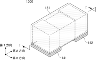
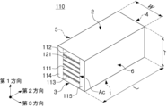
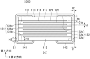
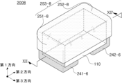
図1は、本発明の一実施形態による積層型電子部品の斜視図を概略的に示すものであり、図2は、図1の積層型電子部品の本体の斜視図を概略的に示すものであり、図3は、図1のI-I'線に沿った断面図であり、図4は、図2の本体を分解して概略的に示す分解斜視図であり、図5は、図1の積層型電子部品が実装された基板の斜視図を概略的に示すものである。 FIG. 1 schematically shows a perspective view of a multilayer electronic component according to one embodiment of the present invention, and FIG. 2 schematically shows a perspective view of a main body of the multilayer electronic component of FIG. 3 is a cross-sectional view taken along the line II' of FIG. 1, FIG. 4 is an exploded perspective view schematically showing an exploded main body of FIG. 2, and FIG. 1 schematically shows a perspective view of a substrate on which the laminated electronic component of 1 is mounted.
以下、図1~図5を参照して、本発明の一実施形態による積層型電子部品1000について説明する。
A multilayer
本発明の一実施形態による積層型電子部品1000は、誘電体層111、上記誘電体層を間に挟んで交互に配置される第1及び第2内部電極121、122を含み、第1方向に対向する第1及び第2面1、2、上記第1及び第2面と連結され、第2方向に対向する第3及び第4面3、4、上記第1~第4面と連結され、第3方向に対向する第5及び第6面5、6を含む本体110と、上記第3面に配置される第1接続部131a、上記第1接続部から上記第1面の一部まで延長される第1バンド部131b、及び上記第1接続部から上記第2面の一部まで延長される第3バンド部131cを含む第1外部電極131と、上記第4面に配置される第2接続部132a、上記第2接続部から上記第1面の一部まで延長される第2バンド部132b、及び上記第2接続部から上記第2面の一部まで延長される第4バンド部132cを含む第2外部電極132と、上記第1及び第2接続部上に配置され、上記第2面、第3及び第4バンド部131c、132cを覆うように配置される絶縁層151と、上記第1バンド部131b上に配置される第1めっき層141と、上記第2バンド部132b上に配置される第2めっき層142と、を含み、上記絶縁層151はハフニウム(Hf)を含む酸化物を含むことができる。
A multilayer
本体110は、誘電体層111及び内部電極121、122が交互に積層されている。本体110の具体的な形状に特に制限はないが、図示のように本体110は六面体形状やこれと類似の形状からなることができる。焼成工程で本体110に含まれたセラミック粉末の収縮により、本体110は完全な直線を有する六面体形状ではないが、実質的に六面体形状を有することができる。
The
本体110は、第1方向に互いに対向する第1及び第2面1、2、上記第1及び第2面1、2と連結され、第2方向に互いに対向する第3及び4面3、4、第1及び第2面1、2と連結され、第3及び第4面3、4と連結され、第3方向に互いに対向する第5及び第6面5、6を有することができる。
The
一実施形態において、本体110は、第1面と第3面を連結する第1-3コーナー、上記第1面と第4面を連結する第1-4コーナー、上記第2面と第3面を連結する第2-3コーナー、上記第2面と第4面を連結する第2-4コーナーを含み、上記第1-3コーナー及び第2-3コーナーは、上記第3面に近づくほど、上記本体の第1方向の中央に収縮した形態を有し、上記第1-4コーナー及び第2-4コーナーは、上記第4面に近づくほど、上記本体の第1方向の中央に収縮した形態を有することができる。
In one embodiment, the
誘電体層111上に内部電極121、122が配置されていないマージン領域が重なることによって、内部電極121、122の厚さによる段差が発生し、第1面と第3~第5面を連結するコーナー及び/又は第2面と第3~第5面を連結するコーナーは、第1面又は第2面を基準としてみたとき、本体110の第1方向の中央側に収縮した形態を有することができる。または、本体の焼結過程における収縮挙動により、第1面1と第3~第6面3、4、5、6を連結するコーナー及び/又は第2面2と第3~第6面3、4、5、6を連結するコーナーは、第1面又は第2面を基準としてみたとき、本体110の第1方向の中央側に収縮した形態を有することができる。または、チッピング不良等を防止するために、本体110の各面を連結する角を別途の工程を行ってラウンド処理することによって、第1面と第3~第6面を連結するコーナー及び/又は第2面と第3~第6面を連結するコーナーはラウンド形状を有することができる。
A margin region where the
上記コーナーは、第1面と第3面を連結する第1-3コーナー、第1面と第4面を連結する第1-4コーナー、第2面と第3面を連結する第2-3コーナー、第2面と第4面を連結する第2-4コーナーを含むことができる。また、コーナーは、第1面と第5面を連結する第1-5コーナー、第1面と第6面を連結する第1-6コーナー、第2面と第5面を連結する第2-5コーナー、第2面と第6面を連結する第2-6コーナーを含むことができる。本体110の第1~第6面は概して平坦な面であることができ、平坦でない領域をコーナーとすることができる。以下、各面の延長線とは、各面の平坦な部分を基準に延長した線を意味することができる。
The corners are the 1-3 corner connecting the first and third surfaces, the 1-4 corner connecting the first and fourth surfaces, and the 2-3 corner connecting the second and third surfaces. The corners may include 2-4 corners connecting the 2nd and 4th faces. In addition, the corners are the 1-5 corner connecting the 1st and 5th surfaces, the 1-6 corner connecting the 1st and 6th surfaces, and the 2-5th corner connecting the 2nd and 5th surfaces. It may include 5 corners, 2-6 corners connecting the 2nd and 6th faces. The first through sixth sides of the
このとき、外部電極131、132のうち本体110のコーナー上に配置された領域をコーナー部、本体110の第3及び第4面上に配置された領域を接続部、本体の第1及び第2面上に配置された領域をバンド部とすることができる。
At this time, the regions of the
一方、内部電極121、122による段差を抑制するために、積層後の内部電極が本体の第5及び第6面5、6に露出するように切断した後、単一の誘電体層又は2つ以上の誘電体層を容量形成部Acの両側面に第3方向(幅方向)に積層してマージン部114、115を形成する場合には、第1面と第5及び第6面を連結する部分及び第2面と第5及び第6面を連結する部分が収縮した形態を有さなくてもよい。
On the other hand, in order to suppress the step due to the
本体110を形成する複数の誘電体層111は焼成された状態であって、隣接する誘電体層111間の境界は走査電子顕微鏡(SEM:Scanning Electron Microscope)を利用せずには確認しにくいほど一体化することができる。
The plurality of
本発明の一実施形態によると、上記誘電体層111を形成する原料は、十分な静電容量が得られる限り特に制限されない。例えば、チタン酸バリウム系材料、鉛複合ペロブスカイト系材料又はチタン酸ストロンチウム系材料などを使用することができる。上記チタン酸バリウム系材料は、BaTiO3系セラミック粉末を含むことができ、上記セラミック粉末の例示として、BaTiO3、BaTiO3にCa(カルシウム)、Zr(ジルコニウム)等が一部固溶した(Ba1-xCax)TiO3(0<x<1)、Ba(Ti1-yCay)O3(0<y<1)、(Ba1-xCax)(Ti1-yZry)O3(0<x<1、0<y<1)又はBa(Ti1-yZry)O3(0<y<1)等が挙げられる。
According to one embodiment of the present invention, the material for forming the
また、上記誘電体層111を形成する原料は、チタン酸バリウム(BaTiO3)などのパウダーに本発明の目的に応じて様々なセラミック添加剤、有機溶剤、結合剤、分散剤などを添加することができる。
In addition, the raw material for forming the
一方、誘電体層111の平均厚さtdは特に限定する必要はない。但し、一般的に誘電体層を0.6μm未満の厚さで薄く形成する場合、特に誘電体層の厚さが0.35μm以下の場合には信頼性が低下する恐れがあった。本発明の一実施形態によると、絶縁層を外部電極の接続部上に配置し、めっき層を外部電極のバンド部上に配置することにより、外部からの水分浸透、めっき液の浸透などを防止して信頼性を向上させることができるため、誘電体層111の平均厚さが0.35μm以下の場合であっても優れた信頼性を確保することができる。
On the other hand, the average thickness td of the
したがって、誘電体層111の平均厚さが0.35μm以下の場合に、本発明による信頼性の向上効果がより顕著になることができる。上記誘電体層111の平均厚さtdは、上記第1及び第2内部電極121、122の間に配置される誘電体層111の平均厚さを意味することができる。
Therefore, when the average thickness of the
誘電体層111の平均厚さは、本体110の長さ及び厚さ方向(L-T)の断面を1万倍率の走査電子顕微鏡(SEM、Scanning Electron Microscope)でイメージをスキャンして測定することができる。より具体的に、スキャンされたイメージにおいて、一つの誘電体層を長さ方向に等間隔である30個の地点でその厚さを測定して平均値を測定することができる。上記等間隔である30個の地点は、容量形成部Acで指定することができる。また、このような平均値の測定を10個の誘電体層に拡張して平均値を測定すると、誘電体層の平均厚さをさらに一般化することができる。
The average thickness of the
本体110は、本体110の内部に配置され、誘電体層111を間に挟んで互いに対向するように配置される第1内部電極121及び第2内部電極122を含んで容量が形成される容量形成部Acと、上記容量形成部Acの第1方向の上部及び下部に形成されたカバー部112、113とを含むことができる。また、上記容量形成部Acは、キャパシタの容量形成に寄与する部分であって、誘電体層111を間に挟んで複数の第1及び第2内部電極121、122を繰り返し積層して形成することができる。
The
カバー部112、113は、上記容量形成部Acの第1方向の上部に配置される上部カバー部112及び上記容量形成部Acの第1方向の下部に配置される下部カバー部113を含むことができる。
The
上記上部カバー部112及び下部カバー部113は、単一の誘電体層又は2つ以上の誘電体層を容量形成部Acの上下面にそれぞれ厚さ方向に積層して形成することができ、基本的に物理的又は化学的ストレスによる内部電極の損傷を防止する役割を果たすことができる。
The
上記上部カバー部112及び下部カバー部113は内部電極を含まず、誘電体層111と同じ材料を含むことができる。すなわち、上記上部カバー部112及び下部カバー部113は、セラミック材料を含むことができ、例えば、チタン酸バリウム(BaTiO3)系セラミック材料を含むことができる。
The
一方、カバー部112、113の平均厚さは特に限定する必要はない。但し、積層型電子部品の小型化及び高容量化をより容易に達成するために、カバー部112、113の平均厚さtcは15μm以下であってもよい。また、本発明の一実施形態によると、絶縁層を外部電極の接続部上に配置し、めっき層を外部電極のバンド部上に配置することにより、外部からの水分浸透、めっき液の浸透などを防止して信頼性を向上させることができるため、カバー部112、113の平均厚さtcが15μm以下の場合であっても優れた信頼性を確保することができる。
On the other hand, the average thickness of the
カバー部112、113の平均厚さtcは第1方向のサイズを意味することができ、容量形成部Acの上部又は下部において等間隔の5個の地点で測定したカバー部112、113の第1方向のサイズを平均した値であることができる。
The average thickness tc of the
また、上記容量形成部Acの側面には、マージン部114、115が配置されることができる。マージン部114、115は、本体110の第5面5に配置された第1マージン部114と、第6面6に配置された第2マージン部115とを含むことができる。すなわち、マージン部114、115は、上記本体110の幅方向の両端面(end surfaces)に配置されることができる。
In addition,
マージン部114、115は、図3に示すように、上記本体110を幅-厚さ(W-T)方向に切断した断面(cross-section)において、第1及び第2内部電極121、122の両端と本体110の境界面との間の領域を意味することができる。マージン部114、115は、基本的に物理的又は化学的ストレスによる内部電極の損傷を防止する役割を果たすことができる。
As shown in FIG. 3, the
マージン部114、115は、セラミックグリーンシート上にマージン部が形成される箇所を除いて、導電性ペーストを塗布して内部電極を形成することにより形成されたものであってもよい。また、内部電極121、122による段差を抑制するために、積層後の内部電極が本体の第5及び第6面5、6に露出するように切断した後、単一の誘電体層又は2つ以上の誘電体層を容量形成部Acの両側面に第3方向(幅方向)に積層してマージン部114、115を形成することもできる。
The
一方、マージン部114、115の幅は特に限定する必要はない。但し、積層型電子部品の小型化及び高容量化をより容易に達成するために、マージン部114、115の平均幅は15μm以下であってもよい。また、本発明の一実施形態によると、絶縁層を外部電極の接続部上に配置し、めっき層を外部電極のバンド部上に配置することにより、外部からの水分浸透、めっき液の浸透などを防止して信頼性を向上させることができる。このため、マージン部114、115の平均幅が15μm以下の場合であっても優れた信頼性を確保することができる。
On the other hand, the width of the
マージン部114、115の平均幅は、マージン部114、115の第3方向の平均サイズを意味することができ、容量形成部Acの側面において等間隔の5個の地点で測定したマージン部114、115の第3方向のサイズを平均した値であることができる。
The average width of the
内部電極121、122は誘電体層111と交互に積層される。内部電極121、122は、第1及び第2内部電極121、122を含むことができる。第1及び第2内部電極121、122は、本体110を構成する誘電体層111を間に挟んで互いに対向するように交互に配置され、本体110の第3及び第4面3、4にそれぞれ露出することができる。
The
図3を参照すると、第1内部電極121は第4面4と離隔し、第3面3を介して露出し、第2内部電極122は第3面3と離隔し、第4面4を介して露出することができる。本体の第3面3には第1外部電極131が配置されて第1内部電極121と連結され、本体の第4面4には第2外部電極132が配置されて第2内部電極122と連結されることができる。
Referring to FIG. 3 , the first
すなわち、第1内部電極121は第2外部電極132とは連結されず、第1外部電極131と連結され、第2内部電極122は第1外部電極131とは連結されず、第2外部電極132と連結される。したがって、第1内部電極121は第4面4において一定距離離隔して形成され、第2内部電極122は第3面3において一定距離離隔して形成されることができる。
That is, the first
このとき、第1及び第2内部電極121、122は、中間に配置された誘電体層111によって互いに電気的に分離されることができる。本体110は、第1内部電極121が印刷されたセラミックグリーンシートと第2内部電極122が印刷されたセラミックグリーンシートとを交互に積層した後、焼成して形成することができる。
At this time, the first and second
内部電極121、122を形成する材料は特に制限されず、電気伝導性に優れた材料を使用することができる。例えば、内部電極121、122は、ニッケル(Ni)、銅(Cu)、パラジウム(Pd)、銀(Ag)、金(Au)、白金(Pt)、錫(Sn)、タングステン(W)、チタン(Ti)及びこれらの合金のうち一つ以上を含むことができる。
Materials for forming the
また、内部電極121、122は、ニッケル(Ni)、銅(Cu)、パラジウム(Pd)、銀(Ag)、金(Au)、白金(Pt)、錫(Sn)、タングステン(W)、チタン(Ti)及びこれらの合金のうち一つ以上を含む内部電極用導電性ペーストをセラミックグリーンシートに印刷して形成することができる。上記内部電極用導電性ペーストの印刷方法としては、スクリーン印刷法又はグラビア印刷法などを使用することができるが、本発明はこれらに限定されるものではない。
The
一方、内部電極121、122の平均厚さteは特に限定する必要はない。但し、一般的に内部電極を0.6μm未満の厚さで薄く形成する場合、特に内部電極の厚さが0.35μm以下の場合には信頼性が低下する恐れがあった。
On the other hand, the average thickness te of the
本発明の一実施形態によると、絶縁層を外部電極の接続部上に配置し、めっき層を外部電極のバンド部上に配置することにより、外部からの水分浸透、めっき液の浸透などを防止して信頼性を向上させることができるため、内部電極121、122の平均厚さが0.35μm以下の場合であっても優れた信頼性を確保することができる。したがって、内部電極121、122の厚さが平均0.35μm以下である場合に、本発明による効果がより顕著となることができ、積層型電子部品の小型化及び高容量化をより容易に達成することができる。
According to one embodiment of the present invention, the insulating layer is arranged on the connection part of the external electrode, and the plating layer is arranged on the band part of the external electrode, thereby preventing the penetration of moisture and the plating solution from the outside. Therefore, even when the average thickness of the
上記内部電極121、122の平均厚さteは内部電極121、122の平均厚さを意味することができる。内部電極121、122の平均厚さは、本体110の長さ及び厚さ方向(L-T)の断面を1万倍率の走査電子顕微鏡(SEM、Scanning Electron Microscope)でイメージをスキャンして測定することができる。より具体的に、スキャンされたイメージにおいて、一つの内部電極を長さ方向に等間隔である30個の地点でその厚さを測定して平均値を測定することができる。上記等間隔である30個の地点は、容量形成部Acで指定することができる。また、このような平均値の測定を10個の内部電極に拡張して平均値を測定すると、内部電極の平均厚さをさらに一般化することができる。
The average thickness te of the
外部電極131、132は、本体110の第3面3及び第4面4に配置されることができる。外部電極131、132は、本体110の第3及び第4面3、4にそれぞれ配置され、第1及び第2内部電極121、122とそれぞれ連結された第1及び第2外部電極131、132を含むことができる。
The
外部電極131、132は、第3面に配置される第1接続部131a及び上記第1接続部から上記第1面の一部まで延長される第1バンド部131bを含む第1外部電極131、第4面に配置される第2接続部132a及び上記第2接続部から上記第1面の一部まで延長される第2バンド部132bを含む第2外部電極132を含むことができる。第1接続部131aは第1内部電極121と第3面で連結され、第2接続部132aは第2内部電極122と第4面で連結されることができる。
The
また、第1外部電極131は、第1接続部131aから第2面の一部まで延長される第3バンド部131cを含むことができ、第2外部電極132は第2接続部132aから第2面の一部まで延長される第4バンド部132cを含むことができる。さらに、第1外部電極131は、第1接続部131aから第5及び第6面の一部まで延長される第1側面バンド部を含むことができ、第2外部電極132は第2接続部132aから第5及び第6面の一部まで延長される第2側面バンド部を含むことができる。
Also, the first
但し、第3バンド部、第4バンド部、第1側部バンド部及び第2側部バンド部は、本発明に必須の構成要素でなくてもよい。第1及び第2外部電極131、132は第2面には配置されなくてもよく、第5及び第6面にも配置されなくてもよい。第1及び第2外部電極131、132が第2面に配置されないことによって、第1及び第2外部電極131、132は本体の第2面の延長線以下に配置されることができる。また、第1及び第2接続部131a、132aは第5及び第6面と離隔して配置されることができ、第1及び第2接続部131a、132aは第2面と離隔して配置されることができる。また、第1及び第2バンド部131b、132bも第5及び第6面と離隔して配置されることができる。
However, the third band portion, the fourth band portion, the first side band portion, and the second side band portion may not be essential components of the present invention. The first and second
一方、第1及び第2外部電極131、132が第3及び第4バンド部131c、132cを含む場合、第3及び第4バンド部131c、132c上に絶縁層が配置されることを図示しているが、これに制限されるものではなく、実装の便宜性を向上させるために、第3及び第4バンド部131c、132c上にめっき層を配置してもよい。また、第1及び第2外部電極131、132が第3及び第4バンド部131c、132cを含むものの、側面バンド部は含まない形態であってもよく、この場合、第1、第2接続部131a、132a、及び第1~第4バンド部131a、132b、131c、132cが第5及び第6面と離隔した形態を有してもよい。
On the other hand, when the first and second
本実施形態では、積層型電子部品1000が2つの外部電極131、132を有する構造を説明しているが、外部電極131、132の個数や形状などは内部電極121、122の形態やその他の目的に応じて変更されることができる。
In this embodiment, a structure in which the multilayer
一方、外部電極131、132は、金属などのように電気伝導性を有するものであれば、如何なる物質を使用して形成されてもよく、電気的特性、構造的安定性などを考慮して具体的な物質が決定されてもよく、さらに、多層構造を有してもよい。
On the other hand, the
外部電極131、132は、導電性金属及びガラスを含む焼成(firing)電極であってもよく、導電性金属及び樹脂を含む樹脂系電極であってもよい。一実施形態において、外部電極131、132はガラスを含むことができる。本発明の絶縁層151は、ハフニウム(Hf)を含む酸化物を含み、ハフニウム(Hf)を含む酸化物は、ガラスと当接する部分で拡散(diffusion)が発生することを抑制し、絶縁層の連続性が低下することを防止することができるため、外部電極131、132がガラスを含む場合、本発明による効果がより顕著になることができる。
The
なお、外部電極131、132は、本体上に焼成電極及び樹脂系電極が順次に形成された形態であってもよい。また、外部電極131、132は、本体上に導電性金属を含むシートを転写する方式で形成されるか、又は焼成電極上に導電性金属を含むシートを転写する方式で形成されたものであってもよい。
The
外部電極131、132に含まれる導電性金属として、電気伝導性に優れた材料を使用することができるが、特に限定されない。例えば、導電性金属は、Cu、Ni、Pd、Ag、Sn、Cr及びそれらの合金のうち一つ以上であってもよい。好ましくは、外部電極131、132は、Ni及びNi合金のうち一つ以上を含むことができる。これにより、Niを含む内部電極121、122との連結性をより向上させることができる。
As the conductive metal contained in the
絶縁層151は、第1及び第2接続部131a、132a上に配置されることができる。第1及び第2接続部131a、132aは内部電極121、122と連結される部位であるため、めっき工程においてめっき液の浸透又は実際の使用時に水分浸透の経路となることができる。本発明では、接続部131a、132a上に絶縁層151が配置されるため、外部からの水分浸透又はめっき液の浸透を防止することができる。
An insulating
絶縁層151は、第1及び第2めっき層141、142と接するように配置されることができる。このとき、絶縁層151が第1及び第2めっき層141、142の端を一部覆う形態で接するか、又は第1及び第2めっき層141、142が絶縁層151の端を一部覆う形態で接することができる。
The insulating
絶縁層151は、第1及び第2接続部131a、132a上に配置され、第2面、第3及び第4バンド部131c、132cを覆うように配置されることができる。このとき、絶縁層151は、第2面のうち第3及び第4バンド部131c、132cが配置されない領域、第3及び第4バンド部131c、132cを覆うように配置されることができる。これにより、絶縁層151が第3及び第4バンド部131c、132cの端と本体110が接する領域をカバーして水分浸透の経路を遮断することにより、耐湿信頼性をより向上させることができる。
The insulating
絶縁層151は、第2面上に配置され、上記第1及び第2接続部131a、132aに延長して配置されることができる。また、絶縁層は、外部電極131、132が第2面に配置されていない場合、第2面を全部覆うように配置されることができる。一方、絶縁層151が第2面に必ずしも配置される必要はなく、絶縁層が第2面の一部又は全部に配置されなくてもよく、絶縁層が2つに分離されて第1及び第2接続部131a、132a上にそれぞれ配置される形態を有してもよい。絶縁層が第2面の全部に配置されない場合、第2面の延長線以下に配置されることができる。また、絶縁層が第2面に配置されないが、第1及び第2接続部131a、132a上で第5及び第6面に延長されて一つの絶縁層を成すことができる。
The insulating
さらに、絶縁層151は、第1及び第2側面バンド部、第5面及び第6面の一部を覆うように配置されることができる。このとき、絶縁層151に覆われていない第5面及び第6面の一部は外部に露出することができる。
In addition, the insulating
また、絶縁層151は、第1及び第2側面バンド部、第5面及び第6面を全て覆うように配置されてもよく、この場合、第5面及び第6面が外部に露出しないため耐湿信頼性を向上させることができ、接続部131a、132aも直接に外部に露出せず、積層型電子部品1000の信頼性を向上させることができる。より詳細には、絶縁層が第1及び第2側面バンド部を全て覆い、第5及び第6面のうち第1及び第2側面バンド部が形成された領域を除いた領域を全て覆うことができる。
Also, the insulating
絶縁層151は、絶縁層151が配置された外部電極131、132上にめっき層141、142が形成されることを防止する役割を果たすことができ、シーリング特性を向上させて外部から水分やめっき液などが浸透することを最小化する役割を果たすことができる。
The insulating
絶縁層151は、ハフニウム(Hf)を含む酸化物を含むことができる。従来は、一般的に絶縁層にガラス系物質を使用していたが、ガラス系列の特性上、焼結時に凝集が著しく発生するため均一な膜を形成しにくく、焼結する過程で熱が必要となるため、本体内の応力を発生させてクラック又はデラミネーションの原因となることがある。また、ガラス系列の物質を含む絶縁層を用いる場合、外部電極を焼成した後にガラス系列の物質を含む絶縁層を焼成させる方法を使用するが、絶縁層を焼成する過程で外部電極の金属物質が内部電極に拡散して放射クラックが発生する恐れがある。さらに、ガラス系列は一般的に硬い特性を有するため、小さな衝撃にも割れる恐れがある。
The insulating
本発明では、絶縁層にガラス系列の物質の代わりにハフニウム(Hf)を含む酸化物を適用することにより、ガラス系列の絶縁層が有する問題を解決しようとした。ハフニウム(Hf)を含む酸化物は絶縁特性を有するだけでなく、透湿率が非常に低いため、薄い厚さでも十分な耐湿信頼性及びめっき液に対する耐酸性を確保することができる。また、ハフニウム(Hf)を含む酸化物は、ガラスと当接する部分で拡散(diffusion)が発生することを抑制し、絶縁層の連続性が低下することを防止することができる。したがって、絶縁層にガラス系列の代わりにハフニウム(Hf)を含む酸化物を適用することにより、耐湿信頼性及びめっき液に対する耐酸性をより向上させることができ、絶縁層の連続性が低下することを防止することができ、熱収縮によるクラック、金属拡散による放射クラックなどを抑制することができる。 The present invention attempts to solve the problems associated with the glass-based insulating layer by applying an oxide containing hafnium (Hf) instead of a glass-based material to the insulating layer. Oxides containing hafnium (Hf) not only have insulating properties, but also have very low moisture permeability, so that even with a small thickness, sufficient moisture resistance reliability and acid resistance to plating solutions can be ensured. In addition, the oxide containing hafnium (Hf) suppresses the occurrence of diffusion in the portion contacting the glass, and can prevent the continuity of the insulating layer from being deteriorated. Therefore, by applying an oxide containing hafnium (Hf) instead of a glass-based insulating layer, it is possible to further improve moisture resistance reliability and acid resistance to a plating solution, and the continuity of the insulating layer is reduced. can be prevented, and cracks due to heat shrinkage, radiation cracks due to metal diffusion, and the like can be suppressed.
一方、絶縁層151を形成する方法は特に限定する必要はない。例えば、本体100に外部電極131、132を形成した後、原子層蒸着法(ALD:Atomic Layer Deposition)を用いてハフニウム(Hf)を含む酸化物を含む絶縁層151を形成することができる。原子層蒸着法は、半導体工程のうち、基板の表面に薄膜や保護膜を蒸着させる技術であって、化学的に薄膜を施す従来の蒸着技術とは異なり、原子層を一層ずつ積み重ねて薄膜を成長させる技術である。原子層蒸着法は、段差被覆(Step-covarage)に優れ、薄膜の厚さ調節が容易であり、均一な薄膜を形成できるという利点がある。したがって、絶縁層151は、原子層蒸着法により形成されたものであってもよく、これにより、薄くて均一な絶縁層151を形成することができる。
On the other hand, the method for forming the insulating
また、絶縁層151に含まれたハフニウム(Hf)を含む酸化物の種類は特に限定されないが、例えば、HfO2であってもよい。
The type of oxide containing hafnium (Hf) contained in the insulating
一実施形態において、絶縁層151は、酸素原子を除いた残りの元素の総モル数に対するハフニウム(Hf)原子のモル数が0.95以上であってもよい。すなわち、絶縁層151は、不純物として検出される元素を除けば、実質的にハフニウム(Hf)を含む酸化物からなることができる。このとき、ハフニウム(Hf)を含む酸化物はHfO2であってもよい。これにより、熱収縮によるクラック、金属拡散による放射クラックなどを抑制する効果、及び耐湿信頼性の向上効果をより向上させることができる。
In one embodiment, the insulating
このとき、絶縁層151の成分は、SEM-EDS(Scanning Electron Microscope-Energy Dispersive X-ray Spectroscopy)を用いて観察した画像から算出したものであってもよい。具体的に、積層型電子部品を幅方向(第3方向)の中央の位置まで研磨して長さ方向及び厚さ方向の断面(L-T断面)を露出させた後、絶縁層を厚さ方向に5等分した領域のうち、中央に配置された領域を、EDSを用いて絶縁層に含まれた各元素のモル数を測定することができ、酸素原子を除いた残りの元素の総モル数に対するハフニウム(Hf)原子のモル数を計算することができる。
At this time, the components of the insulating
一実施形態において、絶縁層151の平均厚さt2は15nm以上1000nm以下であってもよい。絶縁層151の平均厚さt2が15nm以上である場合、絶縁層の水分透過率が0mg/[m2day]であることができ、これにより耐湿信頼性を向上させることができる。
In one embodiment, the average thickness t2 of the insulating
絶縁層151の平均厚さが15nm未満の場合には、熱収縮によるクラック、金属拡散による放射クラック等を抑制する効果及び耐湿信頼性の向上効果が十分に確保できない恐れがあり、絶縁層の水分透過率が0mg/[m2day]を超える可能性がある。これに対し、絶縁層151の平均厚さが1000nmを超える場合には、絶縁層にクラックが発生する恐れがあり、絶縁層の形成時間が過度に長くなる可能性があり、積層型電子部品の全体サイズが大きくなって単位体積当たりの容量が低下する恐れがある。
If the average thickness of the insulating
絶縁層151の平均厚さt2は、第1及び第2接続部131a、132a上の等間隔の5個の地点で測定した厚さを平均した値であってもよい。より具体的な例を挙げると、第1及び第2接続部131a、132aの第1方向の中央地点、上記第1方向の中央地点を基準として第1方向に5μm離隔した2個の地点、第1方向に10μm離隔した2個の地点で測定した絶縁層の厚さ値を平均した値であってもよい。
The average thickness t2 of the insulating
一実施形態において、絶縁層151上に配置され、アルミニウム(Al)を含む酸化物を含むカバー層をさらに含むことができる。より詳細な説明は後述する。
In one embodiment, a cover layer disposed on the insulating
一実施形態において、絶縁層151は第1及び第2外部電極131、132と直接接するように配置され、第1及び第2外部電極131、132は導電性金属及びガラスを含むことができる。これにより、第1及び第2外部電極131、132の外表面のうち絶縁層151が配置された領域には、めっき層141、142が配置されなくてもよいため、めっき液による外部電極の侵食を効果的に抑制することができる。
In one embodiment, the insulating
このとき、第1めっき層141は、絶縁層151の第1外部電極131上に配置された端を覆うように配置され、第2めっき層142は、絶縁層151の第2外部電極132上に配置された端を覆うように配置されることができる。外部電極131、132上にめっき層141、142を形成する前に絶縁層151を先に形成することにより、めっき層の形成過程におけるめっき液の浸透をより確実に抑制することができる。めっき層よりも絶縁層を先に形成することにより、めっき層141、142が絶縁層151の端を覆う形態を有することができる。
At this time, the
一実施形態において、絶縁層151は第1及び第2外部電極131、132と直接接するように配置され、第1及び第2外部電極131、132は導電性金属及び樹脂を含むことができる。これにより、第1及び第2外部電極131、132の外表面のうち絶縁層151が配置された領域には、めっき層141、142が配置されなくてもよいため、めっき液による外部電極の侵食を効果的に抑制することができる。
In one embodiment, the insulating
このとき、第1めっき層141は、絶縁層151の第1外部電極131上に配置された端を覆うように配置され、第2めっき層142は、絶縁層151の第2外部電極132上に配置された端を覆うように配置されることができる。外部電極131、132上にめっき層141、142を形成する前に絶縁層151を先に形成することにより、めっき層の形成過程におけるめっき液の浸透をより確実に抑制することができる。めっき層よりも絶縁層を先に形成することにより、めっき層141、142が絶縁層151の端を覆う形態を有することができる。
At this time, the
第1及び第2めっき層141、142は、それぞれ第1及び第2バンド部131b、132b上に配置されることができる。めっき層141、142は実装特性を向上させる役割を果たすことができ、めっき層141、142がバンド部131b、132b上に配置されることにより、実装空間を最小化することができ、内部電極にめっき液が浸透することを最小化して信頼性を向上させることができる。第1及び第2めっき層141、142の一端は第1面に接することができ、他端は絶縁層151に接することができる。
The first and second plating layers 141, 142 may be disposed on the first and
めっき層141、142の種類は特に限定されず、Cu、Ni、Sn、Ag、Au、Pd及びこれらの合金のうち一つ以上を含むめっき層であってもよく、複数の層で形成されてもよい。めっき層141、142に対するより具体的な例を挙げると、めっき層141、142は、Niめっき層又はSnめっき層であってもよく、第1及び第2バンド部131b、132b上にNiめっき層及びSnめっき層が順次に形成された形態であってもよい。 The types of the plating layers 141 and 142 are not particularly limited, and may be plating layers containing one or more of Cu, Ni, Sn, Ag, Au, Pd, and alloys thereof, and are formed of a plurality of layers. good too. To give a more specific example of the plating layers 141 and 142, the plating layers 141 and 142 may be Ni plating layers or Sn plating layers. and Sn plated layers may be formed sequentially.
一実施形態において、第1及び第2めっき層141、142は、それぞれ第1及び第2接続部131a、132aを一部覆うように延長して配置されることができる。第1及び第2内部電極121、122のうち、第1面1に最も近く配置された内部電極までの第1方向の平均サイズをH1、上記第1面1の延長線から上記第1及び第2接続部131a、132a上に配置された第1及び第2めっき層141、142の端までの第1方向の平均サイズをH2とするとき、H1>H2を満たすことができる。これにより、めっき工程時にめっき液が内部電極に浸透することを抑制し、信頼性を向上させることができる。
In one embodiment, the first and second plating layers 141 and 142 may be extended to partially cover the first and
H1及びH2は、本体110を第3方向に等間隔を有する5個の地点において、第1及び第2方向に切断した断面(L-T断面)で測定した値を平均した値であってもよい。H1は、各断面において第1面1に最も近く配置された内部電極が外部電極と連結される地点で測定した値を平均した値であってもよく、H2は外部電極と接するめっき層の端を基準として測定した値を平均した値であってもよく、H1及びH2の測定時に基準となる第1面の延長線は同一であってもよい。
H1 and H2 are the average values of the values measured in cross sections (LT cross sections) cut in the first and second directions at five points equally spaced in the third direction on the
一実施形態において、第1めっき層141は、絶縁層151の第1外部電極131上に配置された端を覆うように配置され、第2めっき層142は絶縁層151の第2外部電極132上に配置された端を覆うように配置されることができる。これにより、絶縁層151とめっき層141、142との結合力を強化して積層型電子部品1000の信頼性を向上させることができる。
In one embodiment, the
一実施形態において、絶縁層151は、第1めっき層141の第1外部電極131上に配置された端を覆うように配置され、絶縁層151は第2めっき層142の第2外部電極132上に配置された端を覆うように配置されることができる。これにより、絶縁層151とめっき層141、142との結合力を強化して積層型電子部品1000の信頼性を向上させることができる。
In one embodiment, the insulating
一実施形態において、本体110の第2方向の平均サイズをL、上記第3面の延長線から上記第1バンド部の端までの上記第2方向の平均サイズをB1、上記第4面の延長線から上記第2バンド部の端までの上記第2方向の平均サイズをB2とするとき、0.2≦B1/L≦0.4及び0.2≦B2/L≦0.4を満たすことができる。
In one embodiment, the average size of the
B1/L及びB2/Lが0.2未満の場合には、十分な固着強度を確保しにくい可能性がある。これに対し、B2/Lが0.4を超える場合には、高圧電流下で第1バンド部131bと第2バンド部132bとの間で漏れ電流が発生する恐れがあり、めっき工程時にめっき滲み等により第1バンド部131bと第2バンド部132bとが電気的に連結される恐れがある。B1、B2及びLは、本体110を第3方向に等間隔を有する5個の地点において第1及び第2方向に切断した断面(L-T断面)で測定した値を平均した値であってもよい。
If B1/L and B2/L are less than 0.2, it may be difficult to ensure sufficient fixing strength. On the other hand, if B2/L exceeds 0.4, a leakage current may occur between the
積層型電子部品1000が実装された実装基板1100を示す図5を参照すると、積層型電子部品1000のめっき層141、142は、基板180上に配置された電極パッド181、182と半田191、192によって接合されることができる。
Referring to FIG. 5 showing a mounting
一方、内部電極121、122が第1方向に積層されている場合には、内部電極121、122が実装面と平行になるように積層型電子部品1000を基板180に水平実装することができる。但し、本発明が水平実装である場合に限定されるものではなく、内部電極121、122を第3方向に積層する場合には、内部電極121、122が実装面と垂直になるように基板に積層型電子部品を垂直実装することができる。
On the other hand, when the
積層型電子部品1000のサイズは特に限定する必要はない。但し、小型化及び高容量化を同時に達成するためには、誘電体層及び内部電極の厚さを薄くして積層数を増加させなければならないため、1005(長さ×幅、1.0mm×0.5mm)以下のサイズを有する積層型電子部品1000において、本発明による信頼性及び単位体積当たりの容量向上効果がより顕著になることができる。
The size of the multilayer
したがって、製造誤差、外部電極サイズなどを考慮すると、積層型電子部品1000の長さが1.1mm以下であり、幅が0.55mm以下である場合、本発明による信頼性の向上効果がより顕著になることができる。ここで、積層型電子部品1000の長さは、積層型電子部品1000の第2方向の最大サイズを意味し、積層型電子部品1000の幅は、積層型電子部品1000の第3方向の最大サイズを意味することができる。
Therefore, considering manufacturing errors, external electrode sizes, etc., when the multilayer
(実施例)
下記の表1は、ハフニウム(Hf)を含む酸化物を含む絶縁層の平均厚さによる耐湿信頼性及びクラック発生の有無を評価したものである。具体的に各試験番号当たりPI(Polyimide)フィルムに平均厚さを異ならせる絶縁層を原子層蒸着方法(Atomic layer deposition)で形成した後、相対湿度100%、温度41.8℃で水分の透過率を測定した。このとき、水分の透過率の測定装備はMocon社の「AQUATRAN 1(G)」であった。
(Example)
Table 1 below shows the evaluation of the humidity resistance reliability and the occurrence of cracks depending on the average thickness of the insulating layer containing the oxide containing hafnium (Hf). Specifically, after forming an insulating layer with a different average thickness on a PI (Polyimide) film for each test number by atomic layer deposition, moisture permeation was performed at a relative humidity of 100% and a temperature of 41.8 ° C. rate was measured. At this time, the equipment for measuring the moisture permeability was "AQUATRAN 1 (G)" manufactured by Mocon.
また、光学顕微鏡を用いて目視でクラック発生の有無を観察し、クラックが発生した場合は「O」、クラックが発生していない場合は「×」と表した。上記耐湿信頼性の評価は、PIフィルムに絶縁層を形成して評価したものであるが、耐湿信頼性の評価から確認できる効果は、多様な実施例による積層型電子部品1000、2000、3000の場合でも同様に理解することができる。 In addition, the presence or absence of cracks was visually observed using an optical microscope, and "O" was indicated when cracks were generated, and "X" was indicated when no cracks were generated. The above evaluation of moisture resistance reliability was performed by forming an insulating layer on the PI film. can be understood in the same way.

試験番号1は、絶縁層の平均厚さが15nm未満の場合であって、水分透過を抑制する効果が不足していることが確認できる。試験番号2~7は、絶縁層の平均厚さが15nm以上の場合であって、水分透過率が0mg/m2dayであることが確認でき、水分透過を抑制する効果が顕著であることが確認できる。但し、試験番号7は絶縁層の平均厚さが1000nmを超えて絶縁層にクラックが発生した。したがって、一実施形態による積層型電子部品の絶縁層の平均厚さt2を15nm以上1000nm以下とすることにより、水分透過を遮断して優れた耐湿信頼性を確保しながらもクラックを防止することができる。
Test No. 1 is a case where the average thickness of the insulating layer is less than 15 nm, and it can be confirmed that the effect of suppressing moisture permeation is insufficient. In
図6は、本発明の一実施形態による積層型電子部品1001の斜視図を概略的に示すものであり、図7は、図6のII-II'線に沿った断面図である。図6及び図7を参照すると、本発明の一実施形態による積層型電子部品1001は、第1及び第2めっき層141-1、142-1が第1面の延長線E1以下に配置されることができる。これにより、実装時に半田の高さを最小化することができ、実装空間を最小化することができる。また、絶縁層151-1は、第1面の延長線以下まで延長されて第1及び第2めっき層141-1、142-1と接するように配置されることができる。
FIG. 6 schematically shows a perspective view of a multilayer
図8は、本発明の一実施形態による積層型電子部品1002の斜視図を概略的に示すものであり、図9は図8のIII-III'線に沿った断面図である。図8及び図9を参照すると、本発明の一実施形態による積層型電子部品1002は、第1面1上に配置され、第1バンド部131bと第2バンド部132bとの間に配置される追加絶縁層161をさらに含むことができる。これにより、高圧電流下で第1バンド部131bと第2バンド部132bとの間で発生し得る漏れ電流などを防止することができる。
FIG. 8 schematically shows a perspective view of a multilayer
追加絶縁層161の種類は特に限定する必要はない。例えば、追加絶縁層161は、絶縁層151と同様に、ハフニウム(Hf)を含む酸化物を含むことができる。但し、追加絶縁層161と絶縁層151を同じ材料に限定する必要はなく、異なる材料で形成されてもよい。例えば、エポキシ樹脂、アクリル樹脂、エチルセルロース(Ethyl Cellulose)等から選択された1種以上を含んでもよく、ガラスを含んでもよい。
The type of additional insulating
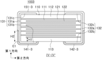
図10は、本発明の一実施形態による積層型電子部品1003の斜視図を概略的に示すものであり、図11は、図10のIV-IV'線に沿った断面図である。図10及び図11を参照すると、一実施形態による積層型電子部品1003は、第1面1から上記第1及び第2内部電極121、122のうち、上記第1面1に最も近く配置された内部電極までの第1方向の平均サイズをH1、上記第1面1の延長線から上記第1及び第2接続部131a、132a上に配置されためっき層141-3、142-3の端までの第1方向の平均サイズをH2とするとき、H1<H2を満たすことができる。これにより、実装時に半田と接する面積を増加させて固着強度を向上させることができる。
FIG. 10 schematically shows a perspective view of a multilayer
より好ましくは、本体110の第1方向の平均サイズをTとするとき、H2<T/2を満たすことができる。すなわち、H1<H2<T/2を満たすことができる。H2がT/2以上の場合には、絶縁層による耐湿信頼性の向上効果が低下する恐れがあるためである。
More preferably, H2<T/2, where T is the average size of the
H1、H2及びTは、本体110を第3方向に等間隔を有する5個の地点において、第1及び第2方向に切断した断面(L-T断面)で測定した値を平均した値であってもよい。H1は、各断面において第1面1に最も近く配置された内部電極が外部電極と連結される地点で測定した値を平均した値であってもよく、H2は、各断面において外部電極と接するめっき層の端を基準として測定した値を平均した値であってもよく、H1及びH2の測定時に基準となる第1面の延長線は同じであってもよい。また、Tは、各断面において、本体110の第1方向の最大サイズを測定した後に平均した値であってもよい。
H1, H2, and T are average values of values measured in cross sections (LT cross sections) cut in the first and second directions at five points equally spaced in the third direction on the
図12は、本発明の一実施形態による積層型電子部品1004の斜視図を概略的に示すものであり、図13は、図12のV-V'線に沿った断面図である。図12及び図13を参照すると、本発明の一実施形態による積層型電子部品1004は、第1バンド部131b-4の平均長さB1が第3バンド部131c-4の平均長さB3より長くてもよく、第2バンド部132b-4の平均長さが第4バンド部132c-4の平均長さB4より長くてもよい。これにより、実装時に半田と接する面積を増加させて固着強度を向上させることができる。
FIG. 12 schematically shows a perspective view of a laminated
より詳細には、第3面3の延長線から上記第1バンド部131b-4の端までの上記第2方向の平均サイズをB1、上記第4面4の延長線から上記第2バンド部132b-4の端までの上記第2方向の平均サイズをB2、上記第3面3の延長線から上記第3バンド部131c-4の端までの上記第2方向の平均サイズをB3、上記第4面4の延長線から上記第4バンド部132c-4の端までの上記第2方向の平均サイズをB4とするとき、B3<B1及びB4<B2を満たすことができる。
More specifically, the average size in the second direction from the extension line of the third surface 3 to the end of the
このとき、本体110の第2方向の平均サイズをLとするとき、0.2≦B1/L≦0.4及び0.2≦B2/L≦0.4を満たすことができる。B1、B2、B3、B4及びLは、本体110を第3方向に等間隔を有する5個の地点において第1及び第2方向に切断した断面(L-T断面)で測定した値を平均した値であってもよい。
At this time, 0.2≦B1/L≦0.4 and 0.2≦B2/L≦0.4 may be satisfied, where L is the average size of the
また、第1外部電極131-4は、第1接続部131a-4から第5及び第6面の一部まで延長される第1側面バンド部を含むことができ、第2外部電極132-4は、第2接続部132a-4から第5及び第6面の一部まで延長される第2側面バンド部を含むことができる。このとき、上記第1及び第2側面バンド部の第2方向のサイズは、第1面に近づくほど次第に大きくなることができる。すなわち、上記第1及び第2側面バンド部は、テーパ形状または台形形状に配置されることができる。
In addition, the first external electrode 131-4 may include a first lateral band portion extending from the
さらに、上記第3面の延長線から上記第3バンド部141c-4の端までの上記第2方向の平均サイズをB3、上記第4面の延長線から上記第4バンド部142c-4の端までの上記第2方向の平均サイズをB4、上記第3面と上記第2内部電極122が離隔した領域の第2方向の平均サイズをG1、上記第4面と上記第1内部電極121が離隔した領域の第2方向の平均サイズをG2とするとき、B3≦G1及びB4≦G2を満たすことができる。これにより、外部電極が占める体積を最小化して積層型電子部品1004の単位体積当たりの容量を増加させることができる。
Further, the average size in the second direction from the extension of the third surface to the end of the third band portion 141c-4 is B3, and the extension of the fourth surface to the end of the fourth band portion 142c-4 is B3. B4 is the average size in the second direction up to, G1 is the average size in the second direction of the region where the third surface and the second
上記G1及びG2は、本体を第3方向の中央で第1及び第2方向に切断した断面において、第1方向の中央部に位置した任意の5個の第2内部電極に対して測定した第3面まで離隔した第2方向のサイズを平均した値はG1とし、第1方向の中央部に位置した任意の5個の第1内部電極に対して測定した第4面まで離隔した領域の第2方向のサイズを平均した値をG2とすることができる。 G1 and G2 above are measured for arbitrary five second internal electrodes positioned at the center in the first direction in a cross section obtained by cutting the main body in the first and second directions at the center in the third direction. The average value of the sizes in the second direction separated by three surfaces is assumed to be G1, and the size of the area separated by the fourth surface measured for arbitrary five first internal electrodes positioned in the central portion in the first direction A value obtained by averaging sizes in two directions can be set to G2.
さらに、本体110を第3方向に等間隔を有する5個の地点において第1及び第2方向に切断した断面(L-T断面)でG1及びG2を求め、それらを平均した値をG1及びG2とすることで、さらに一般化することができる。
Furthermore, G1 and G2 are obtained in cross sections (LT cross sections) obtained by cutting the
但し、本発明をB3≦G1及びB4≦G2に限定する意図ではなく、B3≧G1及びB4≧G2を満たす場合も、本発明の一実施形態に含まれることができる。したがって、一実施形態において、第3面の延長線から第3バンド部の端までの上記第2方向の平均サイズをB3、上記第4面の延長線から上記第4バンド部の端までの上記第2方向の平均サイズをB4、第3面と上記第2内部電極が離隔した領域の第2方向の平均サイズをG1、第4面と上記第1内部電極が離隔した領域の第2方向の平均サイズをG2とするとき、B3≧G1及びB4≧G2を満たすことができる。 However, the present invention is not intended to be limited to B3≦G1 and B4≦G2, and cases where B3≧G1 and B4≧G2 are satisfied may also be included in an embodiment of the present invention. Therefore, in one embodiment, the average size in the second direction from the extension of the third surface to the end of the third band portion is B3, and the average size from the extension of the fourth surface to the end of the fourth band portion is B3. B4 is the average size in the second direction, G1 is the average size in the second direction of the region where the third surface and the second internal electrode are separated, and G1 is the average size in the second direction of the region where the fourth surface and the first internal electrode are separated. When the average size is G2, B3≧G1 and B4≧G2 can be satisfied.
一実施形態において、上記第3面E3の延長線から上記第1バンド部の端までの上記第2方向の平均サイズをB1、上記第4面の延長線から上記第2バンド部の端までの上記第2方向の平均サイズをB2とするとき、B1≧G1及びB2≧G2を満たすことができる。これにより、積層型電子部品1004の基板180との固着強度を向上させることができる。
In one embodiment, the average size in the second direction from the extension of the third surface E3 to the end of the first band portion is B1, and the average size from the extension of the fourth surface to the end of the second band portion is B1. When the average size in the second direction is B2, B1≧G1 and B2≧G2 can be satisfied. Thereby, the bonding strength of the laminated
図14は、本発明の一実施形態による積層型電子部品1005の斜視図を概略的に示すものであり、図15は、図14のVI-VI'線に沿った断面図である。図14及び図15を参照すると、本発明の一実施形態による積層型電子部品1005の第1及び第2外部電極131-5、132-5は、第2面上には配置されず、第3、第4及び第1面に配置されてL字形状を有することができる。すなわち、第1及び第2外部電極131-5、132-5は第2面の延長線以下に配置されることができる。
FIG. 14 schematically shows a perspective view of a multilayer
第1外部電極131-5は、第3面3に配置される第1接続部131a-5、上記第1接続部131a-5から上記第1面1の一部まで延長される第1バンド部131b-5を含むことができ、第2外部電極132-5は、第4面4に配置される第2接続部132a-5、上記第2接続部132a-5から上記第1面1の一部まで延長される第2バンド部132b-5を含むことができる。第2面2上には外部電極131-5、132-5が配置されず、絶縁層151-5が第2面2の全部を覆うように配置されることができる。これにより、外部電極131-5、132-5が占める体積を最小化することができるため、積層電子部品1005の単位体積当たりの容量をより向上させることができる。但し、絶縁層151-5が第2面2の全部を覆う形態に限定する必要はなく、絶縁層が第2面2の一部又は全部を覆わずに、分離されて第1及び第2接続部131a-5、132a-5をそれぞれ覆っている形態を有してもよい。
The first external electrode 131-5 includes a first connecting
また、絶縁層151-5が第5面及び第6面の一部を覆うように配置されて信頼性をより向上させることができる。このとき、絶縁層151-5に覆われていない第5面及び第6面の一部は外部に露出することができる。さらに、絶縁層151-5は、第5面及び第6面の全体を覆うように配置されることができ、この場合、第5面及び第6面が外部に露出しないため、耐湿信頼性をさらに向上させることができる。 In addition, the insulating layer 151-5 is arranged to partially cover the fifth and sixth surfaces, thereby further improving reliability. At this time, portions of the fifth and sixth surfaces that are not covered with the insulating layer 151-5 may be exposed to the outside. Furthermore, the insulating layer 151-5 can be arranged to cover the entire fifth and sixth surfaces. It can be improved further.
第1バンド部131b-5上には第1めっき層141-5、第2バンド部132b-5上には第2めっき層142-5が配置され、第1及び第2めっき層141-5、142-5は第1及び第2接続部132a-5、132b-5上の一部まで延長して配置されることができる。このとき、第5及び第6面5、6上にも外部電極131-5、132-5が配置されなくてもよい。すなわち、外部電極131-5、132-5が第3、第4及び第1面上にのみ配置される形態を有することができる。
A first plating layer 141-5 is arranged on the
第1面1から上記第1及び第2内部電極121、122のうち、上記第1面1に最も近く配置された内部電極までの第1方向の平均サイズをH1、上記第1面1の延長線から上記第1及び第2接続部131a-5、132a-5上に配置されためっき層141-5、142-5の端までの第1方向の平均サイズをH2とするとき、H1<H2を満たすことができる。これにより、実装時に半田と接する面積を増加させて固着強度を向上させることができ、外部電極131-5、132-5とめっき層141-5、142-5が接する面積を増加させてESR(Equivalent Series Resistance)が増加することを抑制することができる。
H1 is the average size in the first direction from the
より好ましくは、本体110の第1方向の平均サイズをTとするとき、H2<T/2を満たすことができる。すなわち、H1<H2<T/2を満たすことができる。H2がT/2以上の場合には、絶縁層による耐湿信頼性の向上効果が低下する恐れがあるためである。
More preferably, H2<T/2, where T is the average size of the
また、第1及び第2めっき層141-5、142-5は、第3面及び第4面において絶縁層151-1の一部を覆うように配置されることができる。すなわち、めっき層141-5、142-5が第3面及び第4面において絶縁層151-5の端を覆うように配置されることができる。これにより、絶縁層151-5とめっき層141-5、142-5との結合力を強化して積層型電子部品1005の信頼性を向上させることができる。
Also, the first and second plating layers 141-5 and 142-5 may be arranged to partially cover the insulating layer 151-1 on the third and fourth surfaces. That is, the plating layers 141-5 and 142-5 can be arranged to cover the edges of the insulating layer 151-5 on the third and fourth surfaces. As a result, the bonding strength between the insulating layer 151-5 and the plating layers 141-5 and 142-5 can be strengthened, and the reliability of the multilayer
また、絶縁層151-5は、第3面及び第4面において第1及び第2めっき層141-5、142-5の一部を覆うように配置されることができる。すなわち、絶縁層151-5が第3面及び第4面においてめっき層141-5、142-5の端を覆うように配置されることができる。これにより、絶縁層151-5とめっき層141-5、142-5との結合力を強化して積層型電子部品1005の信頼性を向上させることができる。
Also, the insulating layer 151-5 may be arranged to partially cover the first and second plating layers 141-5 and 142-5 on the third and fourth surfaces. That is, the insulating layer 151-5 can be arranged to cover the edges of the plating layers 141-5 and 142-5 on the third and fourth surfaces. As a result, the bonding strength between the insulating layer 151-5 and the plating layers 141-5 and 142-5 can be strengthened, and the reliability of the multilayer
図16は、図14の変形例を示すものである。図16を参照すると、本発明の一実施形態による積層型電子部品1005の変形例1006は、第1接続部131a-6と第3面との間には第1追加電極層134が配置されることができ、第2接続部132a-6と第4面との間には第2追加電極層135が配置されることができる。第1追加電極層134は第3面から外れない範囲で配置されることができ、第2追加電極層135は第4面から外れない範囲で配置されることができる。第1及び第2追加電極層134、135は、内部電極121、122と外部電極131-6、132-6間の電気的連結性を向上させることができ、外部電極131-6、132-6との結合力に優れ、外部電極131-6、132-6の機械的結合力をより向上させる役割を果たすことができる。
FIG. 16 shows a modification of FIG. Referring to FIG. 16, in a modified example 1006 of the multilayer
第1及び第2外部電極131-6、132-6は、第2面上に第1及び第2外部電極が配置されていないL字形状を有することができる。第1外部電極131-6は、第1追加電極層134上に配置される第1接続部131a-6、上記第1接続部131a-6から上記第1面1の一部まで延長される第1バンド部131b-6を含むことができ、第2外部電極132-6は、第2追加電極層135上に配置される第2接続部132a-6、上記第2接続部132a-6から上記第1面1の一部まで延長される第2バンド部132b-6を含むことができる。
The first and second external electrodes 131-6 and 132-6 may have an L-shape in which the first and second external electrodes are not arranged on the second surface. The first external electrode 131-6 includes a
一方、第1及び第2追加電極層131-6、132-6は、金属等のように電気伝導性を有するものであれば、如何なる物質を使用して形成されてもよく、電気的特性、構造的安定性等を考慮して具体的な物質が決定されてもよい。また、第1及び第2追加電極層131-6、132-6は、導電性金属及びガラスを含む焼成(firing)電極であってもよく、導電性金属及び樹脂を含む樹脂系電極であってもよい。また、第1及び第2追加電極層131-6、132-6は、本体上に導電性金属を含むシートを転写する方式で形成されたものであってもよい。 On the other hand, the first and second additional electrode layers 131-6 and 132-6 may be formed using any material, such as metal, as long as it has electrical conductivity. A specific substance may be determined in consideration of structural stability and the like. Also, the first and second additional electrode layers 131-6 and 132-6 may be firing electrodes containing conductive metal and glass, or resin-based electrodes containing conductive metal and resin. good too. Also, the first and second additional electrode layers 131-6 and 132-6 may be formed by transferring a sheet containing a conductive metal onto the main body.
第1及び第2追加電極層131-6、132-6に含まれる導電性金属として電気伝導性に優れた材料を使用することができるが、特に限定されない。例えば、導電性金属は、Cu、Ni、Pd、Ag、Sn、Cr及びそれらの合金のうち一つ以上であってもよい。好ましくは、第1及び第2追加電極層131-6、132-6は、Ni及びNi合金のうち一つ以上を含むことができる。これにより、Niを含む内部電極121、122との連結性をより向上させることができる。
A material with excellent electrical conductivity can be used as the conductive metal contained in the first and second additional electrode layers 131-6 and 132-6, but is not particularly limited. For example, the conductive metal may be one or more of Cu, Ni, Pd, Ag, Sn, Cr and alloys thereof. Preferably, the first and second additional electrode layers 131-6 and 132-6 may include one or more of Ni and Ni alloys. Thereby, connectivity with the
図17は、本発明の一実施形態による積層型電子部品1007の斜視図を概略的に示すものであり、図18は、図17のVII-VII'線に沿った断面図である。図17及び図18を参照すると、本発明の一実施形態による積層型電子部品1007の第1及び第2めっき層141-6、142-6の平均厚さt1は絶縁層151-6の平均厚さt2よりも薄い形態であってもよい。
FIG. 17 schematically shows a perspective view of a laminated
絶縁層151-6は外部からの水分浸透又はめっき液の浸透を防止する役割を果たすが、めっき層141-6、142-6との連結性が弱く、めっき層141-6、142-6のデラミネーション(delamination)の原因となることがある。めっき層がデラミネーションされる場合、基板180との固着強度が低下する可能性がある。ここで、めっき層141-6、142-6のデラミネーションとは、めっき層が一部剥がれたり、外部電極131-5、132-5と物理的に分離されたりすることを意味することができる。めっき層と絶縁層との連結性が弱いため、絶縁層とめっき層との界面の隙間が広がったり、異物が浸透する可能性が高くなり、外部衝撃等に脆弱になったりしてデラミネーションされる可能性が高くなることがある。
The insulating layer 151-6 plays a role of preventing penetration of water or plating solution from the outside, but the connectivity with the plating layers 141-6 and 142-6 is weak, and the plating layers 141-6 and 142-6 are weak. It may cause delamination. If the plating layer is delaminated, the bonding strength with the
本発明の一実施形態によると、めっき層の平均厚さt1を絶縁層の平均厚さt2よりも薄くしてめっき層と絶縁層が当接する面積を減らすことができ、これにより、デラミネーションの発生を抑制して積層型電子部品1000の基板180との固着強度を向上させることができる。
According to one embodiment of the present invention, the average thickness t1 of the plating layer can be made thinner than the average thickness t2 of the insulating layer to reduce the contact area between the plating layer and the insulating layer, thereby improving the delamination. It is possible to suppress the generation and improve the bonding strength of the multilayer
第1及び第2めっき層141-6、142-6の平均厚さt1は、第1及び第2接続部131a-5、132a-5又は第1及び第2バンド部131b-5、132b-5上の等間隔の5個の地点で測定した厚さを平均した値であってもよく、絶縁層151-6の平均厚さt2は第1及び第2接続部131a-5、132a-5上の等間隔の5個の地点で測定した厚さを平均した値であってもよい。
The average thickness t1 of the first and second plating layers 141-6, 142-6 is The average thickness t2 of the insulating layer 151-6 measured at five equally spaced points above may be the average thickness t2 of the first and second connecting
図19は、本発明の一実施形態による積層型電子部品1008の斜視図を概略的に示すものであり、図20は、図18のXIV-XIV'線に沿った断面図である。図19及び図20を参照すると、一実施形態による積層型電子部品1008の絶縁層151-7上にはアルミニウム(Al)を含む酸化物を含むカバー層171が配置されることができる。
FIG. 19 schematically shows a perspective view of a laminated
アルミニウム(Al)を含む酸化物は、ガラスと当接する部分で拡散(diffusion)が発生する可能性があり、ガラスを含む外部電極上にアルミニウム(Al)を含む酸化物で絶縁層を形成する場合、拡散により絶縁層の連続性が低下する可能性がある。特に、積層型電子部品を高温環境で使用する場合、拡散が発生しやすいため、アルミニウム(Al)を含む酸化物で絶縁層を形成する場合、高温環境における耐湿信頼性が保障できない恐れがある。 An oxide containing aluminum (Al) may cause diffusion in a portion in contact with glass. Therefore, when forming an insulating layer of an oxide containing aluminum (Al) on an external electrode containing glass, , diffusion may reduce the continuity of the insulating layer. In particular, when a laminated electronic component is used in a high-temperature environment, diffusion is likely to occur. Therefore, if an oxide containing aluminum (Al) is used to form an insulating layer, there is a risk that moisture resistance reliability in a high-temperature environment cannot be guaranteed.
本発明の一実施形態によると、アルミニウム(Al)を含む酸化物を含むカバー層171が、ハフニウム(Hf)を含む酸化物を含む絶縁層151-7上に配置されるため、外部電極131、132がガラスを含む場合にもカバー層171の連続性が低下することを防止することができ、高温環境でも優れた耐湿信頼性を確保することができる。また、カバー層171にクラックが発生しても、絶縁層151-7が第1、第2外部電極131、132及び本体110の内部にクラックが伝播することを防止する役割を果たすことができ、クラックの発生を抑制することができる。
According to one embodiment of the present invention, a
一実施形態において、絶縁層151-7に含まれたハフニウム(Hf)を含む酸化物はHfO2であってもよく、カバー層171に含まれたアルミニウム(Al)を含む酸化物はAl2O3であってもよい。
In one embodiment, the hafnium (Hf)-containing oxide included in the insulating layer 151-7 may be HfO 2 , and the aluminum (Al)-containing oxide included in the
一実施形態において、絶縁層151-7は、酸素原子を除いた残りの元素の総モル数に対するハフニウム(Hf)原子のモル数が0.95以上であってもよく、カバー層171は酸素原子を除いた残りの元素の総モル数に対するアルミニウム(Al)原子のモル数は0.95以上であってもよい。すなわち、不純物として検出される元素を除けば、絶縁層151-7は実質的にハフニウム(Hf)を含む酸化物からなることができ、カバー層171は実質的にアルミニウム(Al)からなることができる。これにより、熱収縮によるクラック、金属拡散による放射クラックなどを抑制する効果、及び耐湿信頼性の向上効果をより向上させることができる。このとき、カバー層171の成分は、上述した絶縁層の成分を分析する方法と同様の方法で分析することができる。
In one embodiment, the insulating layer 151-7 may contain 0.95 or more moles of hafnium (Hf) atoms with respect to the total moles of elements other than oxygen atoms, and the
図21は、本発明の一実施形態による積層型電子部品2000の斜視図を概略的に示すものであり、図22は、図21のVIII-VIII'線に沿った断面図である。以下、図21及び図22を参照して、本発明の一実施形態による積層型電子部品2000について詳細に説明する。但し、上述した内容と重複する内容は、重複した説明を避けるために省略することができる。
FIG. 21 schematically shows a perspective view of a multilayer
本発明の一実施形態による積層型電子部品2000は、誘電体層111、上記誘電体層を間に挟んで交互に配置される第1及び第2内部電極121、122を含み、第1方向に対向する第1及び第2面1、2、上記第1及び第2面と連結され、第2方向に対向する第3及び第4面3、4、上記第1~第4面と連結され、第3方向に対向する第5及び第6面5、6を含む本体110と、上記第3面に配置される第1連結電極231a及び上記第1面に配置されて上記第1連結電極と連結される第1バンド電極231bを含む第1外部電極231と、上記第4面に配置される第2連結電極232a及び上記第1面に配置されて上記第2連結電極と連結される第2バンド電極232bを含む第2外部電極232と、上記第1連結電極上に配置される第1絶縁層251と、上記第2連結電極上に配置される第2絶縁層252と、上記第1バンド電極上に配置される第1めっき層241と、上記第2バンド電極上に配置される第2めっき層242と、を含み、上記第1及び第2絶縁層251、252はハフニウム(Hf)を含む酸化物を含むことができる。
A multilayer
第1連結電極231aは第3面3に配置されて第1内部電極121と連結され、第2連結電極231bは第4面4に配置されて第2内部電極122と連結されることができる。また、第1連結電極231a'上には第1絶縁層251が配置され、第2連結電極232a上には第2絶縁層252が配置されることができる。
The
従来は、外部電極を形成する際に導電性金属が含まれたペーストを使用して、本体の内部電極が露出した面をペーストにディッピング(dipping)する方法が主に使用されていた。しかし、ディッピング(dipping)工法によって形成された外部電極は、厚さ方向の中央部における外部電極の厚さが過度に厚くなることがあった。また、このようなディッピング(dipping)工法による外部電極の厚さ不均衡の問題でなくとも、本体の第3及び第4面に内部電極が露出するため、外部電極を介した水分及びめっき液の浸透を抑制するために第3及び第4面に配置された外部電極の厚さが一定以上になるように形成した。 Conventionally, a method of using a paste containing a conductive metal when forming the external electrodes and dipping the exposed surface of the internal electrodes of the main body into the paste has been mainly used. However, the external electrodes formed by the dipping method may be excessively thick at the central portion in the thickness direction. In addition, even if there is no problem of thickness imbalance of the external electrodes due to the dipping method, since the internal electrodes are exposed on the third and fourth surfaces of the main body, moisture and plating solution can flow through the external electrodes. In order to suppress permeation, the external electrodes arranged on the third and fourth surfaces are formed to have a thickness greater than a certain value.
これに対し、本発明では、連結電極231a、232a上に絶縁層251、252を配置するため、内部電極が露出する第3及び第4面における連結電極231a、232aの厚さを薄くしても十分な信頼性を確保することができる。
In contrast, in the present invention, since the insulating
第1及び第2連結電極231a、232aは、それぞれ第3及び第4面に対応する形態であってもよく、第1及び第2連結電極231a、232aにおいて本体110に向かう面は本体110の第3及び第4面とそれぞれ同じ面積を有してもよい。第1及び第2連結電極231a、232aは、それぞれ第3及び第4面3、4から外れない範囲で配置されることができる。連結電極231a、232aは、本体110の第1、第2、第5及び第6面1、2、5、6に延長されないように配置されることができる。具体的に、一実施形態において、第1及び第2連結電極231a、232aは、第5及び第6面と離隔して配置されることができる。これにより、内部電極121、122と外部電極231、232間の十分な連結性を確保しながらも外部電極が占める体積を最小化し、積層型電子部品2000の単位体積当たりの容量を増加させることができる。
The first and
このような観点から、上記第1及び第2連結電極231a、232aは、上記第2面2と離隔して配置されることができる。すなわち、外部電極231、232が第2面上には配置されないことによって、外部電極231、232が占める体積をさらに最小化し、積層型電子部品2000の単位体積当たりの容量をさらに増加させることができる。
From this point of view, the first and
但し、連結電極231a、232aは、本体110のコーナーに延長されてコーナー上に配置されたコーナー部を含むことができる。すなわち、一実施形態において、第1連結電極は、上記第1-3コーナー及び第2-3コーナー上に延長して配置されるコーナー部を含み、上記第2連結電極は、上記第1-4コーナー及び第2-4コーナー上に延長して配置されるコーナー部を含むことができる。
However, the
また、連結電極231a、232aは、従来のディッピング方式によって形成された外部電極に比べて均一かつ薄い厚さを有することができる。連結電極231a、232aを形成する方法は特に制限する必要はないが、例えば、導電性金属、バインダーのような有機物質等を含むシートを第3及び第4面に転写する方式で形成することができるが、これに制限されるものではなく、導電性金属を第3及び第4面にめっきして形成することができる。すなわち、連結電極231a、232aは、導電性金属を焼成した焼成層であってもよく、めっき層であってもよい。
In addition, the
連結電極231a、232aの厚さは特に限定されないが、例えば2~7μmであってもよい。ここで、連結電極231a、232aの厚さとは、最大厚さを意味することができ、連結電極231a、232aの第2方向のサイズを意味することができる。
The thickness of the connecting
一実施形態において、第1及び第2連結電極231a、232aは、内部電極121、122に含まれた金属と同じ金属及びガラスを含むことができる。第1及び第2連結電極231a、232aが内部電極121、122に含まれた金属と同じ金属を含むことにより、内部電極121、122との電気的連結性を向上させることができ、第1及び第2連結電極231a、232aがガラスを含むことにより、本体110及び/又は絶縁層251、252との結合力を向上させることができる。このとき、内部電極121、122に含まれた金属と同じ金属はNiであってもよい。
In one embodiment, the first and
第1及び第2絶縁層251、252は、それぞれ第1及び第2連結電極231a、232a上に配置され、第1及び第2連結電極231a、232a上にめっき層が形成されることを防止する役割を果たすことができる。また、第1及び第2絶縁層251、252は、シーリング特性を向上させ、外部から水分やめっき液等が浸透することを最小化する役割を果たすことができる。第1及び第2絶縁層251、252は、ハフニウム(Hf)を含む酸化物を含むことができる。これにより、耐湿信頼性をより向上させることができ、熱収縮によるクラック、金属拡散による放射クラックなどを抑制することができる。
The first and second insulating
第1及び第2バンド電極231b、232bは本体110の第1面1に配置されることができる。第1及び第2バンド電極231b、232bは、それぞれ第1及び第2連結電極231a、232aと接触することにより、第1及び第2内部電極121、122とそれぞれ電気的に連結されることができる。
The first and
従来のディッピング(dipping)工法によって形成された外部電極は、第3及び第4面において厚く形成され、第1、第2、第5及び第6面にも一部延長して形成されることから、有効体積率を高く確保することが難しいという問題があった。これに対し、本発明の一実施形態によると、内部電極が露出した面には第1及び第2連結電極231a、232aを配置し、基板に実装される面には第1及び第2バンド電極231b、232bを配置することにより、有効体積率を高く確保することができる。
The external electrodes formed by the conventional dipping method are formed thick on the third and fourth surfaces and partially extended on the first, second, fifth and sixth surfaces. , there is a problem that it is difficult to secure a high effective volume ratio. In contrast, according to an embodiment of the present invention, the first and
一方、内部電極121、122が第1方向に積層されている場合には、内部電極121、122が実装面と平行になるように積層型電子部品2000を基板に水平実装することができる。但し、本発明が水平実装である場合に限定されるものではなく、内部電極121、122を第3方向に積層する場合には、内部電極121、122が実装面と垂直になるように基板に積層型電子部品を垂直実装することができる。
On the other hand, when the
第1及び第2バンド電極231b、232bは、金属等のように電気伝導性を有するものであれば、如何なる物質を使用して形成されてもよく、電気的特性、構造的安定性等を考慮して具体的な物質が決定されてもよい。例えば、第1及び第2バンド電極231b、232bは、導電性金属及びガラスを含む焼成(firing)電極であってもよく、本体の第1面に導電性金属及びガラスを含むペーストを塗布する方式を用いて形成してもよいが、これに限定されるものではなく、導電性金属を本体の第1面にめっきしためっき層であってもよい。
The first and
第1及び第2バンド電極231b、232bに含まれる導電性金属として電気伝導性に優れた材料を使用することができるが、特に限定されない。例えば、導電性金属は、ニッケル(Ni)、銅(Cu)、及びそれらの合金のうち一つ以上であってもよく、内部電極121、122に含まれた金属と同じ金属を含んでもよい。
A material with excellent electrical conductivity can be used as the conductive metal contained in the first and
一方、一実施形態において、第1外部電極231は、上記第2面2に配置されて上記第1連結電極231aと連結される第3バンド電極(図示せず)をさらに含み、上記第2外部電極232は、上記第2面2に配置されて上記第2連結電極232aと連結される第4バンド電極(図示せず)をさらに含むことができる。
Meanwhile, in one embodiment, the first
一実施形態において、上記第3面の延長線E3から上記第1バンド電極231bの端までの距離をB1、上記第4面の延長線E4から上記第2バンド電極232bの端までの距離をB2、上記第3面の延長線から上記第3バンド電極(図示せず)の端までの距離をB3、上記第4面の延長線から上記第4バンド電極(図示せず)の端までの距離をB4、上記第3面と上記第2内部電極122が離隔した領域の第2方向の平均サイズをG1、上記第4面と上記第1内部電極121が離隔した領域の第2方向の平均サイズをG2とするとき、B1≧G1、B3≦G1、B2≧G2及びB4≦G2を満たすことができる。これにより、外部電極が占める体積を最小化して積層型電子部品2000の単位体積当たりの容量を増加させるとともに、実装時に半田と接する面積を増加させて固着強度を向上させることができる。
In one embodiment, the distance from the extension line E3 of the third surface to the end of the
但し、本発明をB1≧G1、B3≦G1、B2≧G2及びB4≦G2に限定しようとする意図ではなく、B1≧G1、B3≧G1、B2≧G2及びB4≧G2を満たす場合も本発明の一実施形態に含まれることができる。したがって、一実施形態において、上記第3面の延長線E3から上記第1バンド電極231bの端までの距離をB1、上記第4面の延長線E4から上記第2バンド電極232bの端までの距離をB2、上記第3面の延長線から上記第3バンド電極(図示せず)の端までの距離をB3、上記第4面の延長線から上記第4バンド電極(図示せず)の端までの距離をB4、上記第3面と上記第2内部電極122が離隔した領域の第2方向の平均サイズをG1、上記第4面と上記第1内部電極121が離隔した領域の第2方向の平均サイズをG2とするとき、B1≧G1、B3≧G1、B2≧G2及びB4≧G2を満たすことができる。これにより、第1及び第2面のいずれか一面を実装面とすることができ、実装の便宜性を向上させることができる。
However, the present invention is not intended to be limited to B1≧G1, B3≦G1, B2≧G2 and B4≦G2. can be included in an embodiment of Therefore, in one embodiment, the distance from the extension line E3 of the third surface to the end of the
第1及び第2めっき層241、242は、第1及び第2バンド電極231b、232b上に配置されることができる。第1及び第2めっき層241、242は実装特性を向上させる役割を果たす。第1及び第2めっき層241、242の種類は特に限定されず、Ni、Sn、Pd及びこれらの合金のうち一つ以上を含むめっき層であってもよく、複数の層で形成されてもよい。
The first and second plating layers 241, 242 may be disposed on the first and
第1及び第2めっき層241、242に対するより具体的な例を挙げると、第1及び第2めっき層241、242は、Niめっき層又はSnめっき層であってもよく、第1及び第2バンド電極231b、232b上にNiめっき層及びSnめっき層が順次に形成された形態であってもよい。
As a more specific example of the first and second plating layers 241 and 242, the first and second plating layers 241 and 242 may be Ni plating layers or Sn plating layers. A form in which a Ni plating layer and a Sn plating layer are sequentially formed on the
一実施形態において、第1及び第2めっき層241、242は、それぞれ第1及び第2連結電極231a、232aを一部覆うように延長して配置されることができる。第1面1から第1及び第2内部電極121、122のうち第1面1に最も近く配置された内部電極までの第1方向の平均サイズをH1、上記第1面1の延長線から上記第1及び第2連結電極231a、232a上に配置された第1及び第2めっき層241、242の端までの第1方向の平均サイズをH2とするとき、H1>H2を満たすことができる。これにより、めっき工程時にめっき液が内部電極に浸透することを抑制して信頼性を向上させることができる。
In one embodiment, the first and second plating layers 241 and 242 may be extended to partially cover the first and
一実施形態において、第1及び第2絶縁層251、252は、第1及び第2連結電極231a、232aとそれぞれ直接接するように配置され、第1及び第2連結電極231a、232aは導電性金属及びガラスを含むことができる。これにより、第1及び第2連結電極231a、232aの外表面のうち絶縁層251、252が配置された領域には、めっき層241、242が配置されなくてもよいため、めっき液による外部電極の侵食を効果的に抑制することができる。
In one embodiment, the first and second insulating
一実施形態において、第1及び第2絶縁層251、252は、第1及び第2連結電極231a、232aとそれぞれ直接接するように配置され、第1及び第2連結電極231a、232aは導電性金属及び樹脂を含むことができる。これにより、第1及び第2連結電極231a、232aの外表面のうち絶縁層251、252が配置された領域には、めっき層241、242が配置されなくてもよいため、めっき液による外部電極の侵食を効果的に抑制することができる。
In one embodiment, the first and second insulating
一実施形態において、第1めっき層241は、第1絶縁層251の第1外部電極231上に配置された端を覆うように配置され、第2めっき層242は第2絶縁層252の第2外部電極232上に配置された端を覆うように配置されることができる。これにより、絶縁層251、252とめっき層241、242との結合力を強化して積層型電子部品3000の信頼性を向上させることができる。また、外部電極231、232上にめっき層241、242を形成する前に第1及び第2絶縁層251、252を先に形成することにより、めっき層の形成過程におけるめっき液の浸透をより確実に抑制することができる。めっき層よりも絶縁層を先に形成することにより、めっき層241、242が絶縁層251、252の端を覆う形態を有することができる。
In one embodiment, the
一実施形態において、第1絶縁層251は、第1めっき層241の第1外部電極231上に配置された端を覆うように配置され、第2絶縁層252は第2めっき層242の第2外部電極232上に配置された端を覆うように配置されることができる。これにより、絶縁層251とめっき層241、242との結合力を強化して積層型電子部品3000の信頼性を向上させることができる。
In one embodiment, the first insulating
図23は、図21の変形例を示すものである。図23を参照すると、本発明の一実施形態による積層型電子部品2000の変形例2001は、第1及び第2絶縁層251-1、252-1が第5及び第6面5、6に延長して互いに連結されることにより、一つの絶縁層253-1として連結されることができる。このとき、連結された第1及び第2絶縁層253-1が第5面及び第6面の一部を覆うように配置されてもよい。
FIG. 23 shows a modification of FIG. Referring to FIG. 23, a modified example 2001 of a multilayer
図24は、本発明の一実施形態による積層型電子部品2002の斜視図を概略的に示すものであり、図25は、図24のIX-IX'線に沿った断面図である。図24及び図25を参照すると、本発明の一実施形態による積層型電子部品2002は、第1及び第2めっき層241-2、242-2が第1面の延長線以下に配置されることができる。これにより、実装時に半田の高さを最小化することができ、実装空間を最小化することができる。また、第1及び第2絶縁層251-2、252-2は、第1面の延長線以下まで延長して第1及び第2めっき層241-2、242-2と接するように配置されることができる。
FIG. 24 schematically shows a perspective view of a laminated
図26は、図24の変形例を示すものである。図26を参照すると、本発明の一実施形態による積層型電子部品2002の変形例2003は、第1及び第2絶縁層251-3、252-3が第5及び第6面5、6に延長して互いに連結されることにより、一つの絶縁層253-3として連結されることができる。このとき、連結された第1及び第2絶縁層253-3が第5面及び第6面の全部を覆うように配置されることができる。
FIG. 26 shows a modification of FIG. Referring to FIG. 26, a modified example 2003 of a multilayer
図27は、本発明の一実施形態による積層型電子部品2004の斜視図を概略的に示すものであり、図28は、図27のX-X'線に沿った断面図である。図27及び図28を参照すると、本発明の一実施形態による積層型電子部品2004は、第1面1上に配置され、第1バンド電極231bと第2バンド電極232bとの間に配置される追加絶縁層261をさらに含むことができる。これにより、高圧電流下で第1バンド電極231bと第2バンド電極232bとの間で発生し得る漏れ電流などを防止することができる。
FIG. 27 schematically shows a perspective view of a laminated
追加絶縁層261の種類は特に限定する必要はない。例えば、追加絶縁層261は、第1及び第2絶縁層251-2、252-2と同様にハフニウム(Hf)を含む酸化物を含むことができる。但し、追加絶縁層261と第1及び第2絶縁層251-2、252-2とを同じ材料に限定する必要はなく、異なる材料で形成されてもよい。例えば、エポキシ樹脂、アクリル樹脂、エチルセルロース(Ethyl Cellulose)等から選択された1種以上を含んでもよく、ガラスを含んでもよい。
The type of additional insulating
図29は、図27の変形例を示すものである。図29を参照すると、本発明の一実施形態による積層型電子部品2004の変形例2005は、第1及び第2絶縁層251-5、252-5が第5及び第6面5、6に延長して互いに連結されることにより、一つの絶縁層253-5として連結されることができる。
FIG. 29 shows a modification of FIG. Referring to FIG. 29, a modified example 2005 of the multilayer
図30は、本発明の一実施形態による積層型電子部品2006の斜視図を概略的に示すものであり、図31は、図30のXI-XI'線に沿った断面図である。図30及び図31を参照すると、一実施形態による積層型電子部品2006は、第1連結電極231a上に配置される第1絶縁層251-6、第2連結電極232a上に配置されるに配置される第2絶縁層252-6を含み、第1面1から上記第1及び第2内部電極121、122のうち上記第1面1に最も近く配置された内部電極までの第1方向の平均サイズをH1、上記第1面1の延長線から上記第1及び第2連結電極231a、232a上に配置された第1及び第2めっき層241-6、242-6の端までの第1方向の平均サイズをH2とするとき、H1<H2を満たすことができる。これにより、実装時に半田と接する面積を増加させて固着強度を向上させることができる。
FIG. 30 schematically shows a perspective view of a laminated
より好ましくは、本体110の第1方向の平均サイズをTとするとき、H2<T/2を満たすことができる。すなわち、H1<H2<T/2を満たすことができる。H2がT/2以上の場合には、絶縁層による耐湿信頼性の向上効果が低下する恐れがあるためである。
More preferably, H2<T/2, where T is the average size of the
図32は、図30の変形例を示すものである。図32を参照すると、本発明の一実施形態による積層型電子部品2006の変形例2007は、第1及び第2絶縁層251-7、252-7が第5及び第6面5、6に延長して互いに連結されることにより、一つの絶縁層253-7として連結されることができる。
FIG. 32 shows a modification of FIG. Referring to FIG. 32, a modified example 2007 of the multilayer
図33は、本発明の一実施形態による積層型電子部品2008の斜視図を概略的に示すものであり、図34は、図33のXII-XII'線に沿った断面図である。図33及び図34を参照すると、本発明の一実施形態による積層型電子部品2008は、第1及び第2絶縁層251-8、252-8が第2、第5及び第6面2、5、6に延長して互いに連結されることにより、一つの絶縁層253-8として連結されることができる。図35に示すように、絶縁層253-8が第2面を全て覆っている形態であってもよく、第5及び第6面は一部のみを覆っている形態であってもよい。
FIG. 33 schematically shows a perspective view of a laminated
図35は、本発明の一実施形態による積層型電子部品2009の斜視図を概略的に示すものであり、図36は、図35のXIII-XIII'線に沿った断面図である。図37及び図40を参照すると、本発明の一実施形態による積層型電子部品2009の第1及び第2めっき層241-9、242-9の平均厚さt1は、第1及び第2絶縁層251-9、252-9の平均厚さt2より薄い形態であってもよい。
FIG. 35 schematically shows a perspective view of a laminated
本発明の一実施形態によると、第1及び第2めっき層241-9、242-9の平均厚さt1を第1及び第2絶縁層251-9、252-9の平均厚さt2よりも薄くしてめっき層と絶縁層が当接する面積を減らすことができ、これによりデラミネーションの発生を抑制して積層型電子部品2009の基板180との固着強度を向上させることができる。
According to one embodiment of the present invention, the average thickness t1 of the first and second plating layers 241-9, 242-9 is greater than the average thickness t2 of the first and second insulating layers 251-9, 252-9. It is possible to reduce the contact area between the plating layer and the insulating layer by making it thinner, thereby suppressing the occurrence of delamination and improving the bonding strength of the multilayer
第1及び第2めっき層241-9、242-9の平均厚さt1は、第1及び第2連結電極231a、232a又は第1及び第2バンド電極231b、232b上の等間隔の5個の地点で測定した厚さを平均した値であってもよく、絶縁層251-9、252-9の平均厚さt2は第1及び第2連結電極231a、232a上の等間隔の5個の地点で測定した厚さを平均した値であってもよい。
The average thickness t1 of the first and second plating layers 241-9, 242-9 is five equal intervals on the first and second connecting
図37は、図35の変形例を示すものである。図37を参照すると、本発明の一実施形態による積層型電子部品2009の変形例2010は、第1及び第2絶縁層251-10、252-10が第5及び第6面5、6に延長して互いに連結されることにより、一つの絶縁層253-10として連結されることができる。
FIG. 37 shows a modification of FIG. Referring to FIG. 37, a modified example 2010 of the multilayer
図38は、本発明の一実施形態による積層型電子部品2011の斜視図を概略的に示すものであり、図39は、図38のXV-XV'線に沿った断面図である。図38及び図39を参照すると、一実施形態による積層型電子部品2011の第1及び第2絶縁層251-11、252-11上には、それぞれ絶縁物質を含む第1及び第2カバー層271、272が配置されることができる。
FIG. 38 schematically shows a perspective view of a laminated
アルミニウム(Al)を含む酸化物を含む第1及び第2カバー層271、272がハフニウム(Hf)を含む酸化物を含む第1及び第2絶縁層251-11、252-11上に配置されるため、第1及び第2外部電極231、232がガラスを含む場合でも、第1及び第2カバー層271、272の連続性が低下することを防止することができ、高温環境でも優れた耐湿信頼性を確保することができる。また、第1及び第2カバー層271、272にクラックが発生しても、第1及び第2絶縁層251-11、252-11が第1、第2外部電極231、232及び本体110の内部にクラックが伝播することを防止する役割を果たすことができ、クラックの発生を抑制することができる。
First and second cover layers 271, 272 comprising an oxide comprising aluminum (Al) are disposed on the first and second insulating layers 251-11, 252-11 comprising an oxide comprising hafnium (Hf). Therefore, even when the first and second
一実施形態において、第1及び第2絶縁層251-11、252-11に含まれたハフニウム(Hf)を含む酸化物はHfO2であってもよく、第1及び第2カバー層271、272に含まれたアルミニウム(Al)を含む酸化物はAl2O3であってもよい。
In one embodiment, the oxide containing hafnium (Hf) included in the first and second insulating layers 251-11 and 252-11 may be HfO 2 , and the first and second cover layers 271 and 272 may be
一実施形態において、第1及び第2絶縁層251-11、252-11は、酸素原子を除いた残りの元素の総モル数に対するハフニウム(Hf)原子のモル数が0.95以上であってもよく、第1及び第2カバー層271、272は、酸素原子を除いた残りの元素の総モル数に対するアルミニウム(Al)原子のモル数が0.95以上であってもよい。すなわち、不純物として検出される元素を除けば、第1及び第2絶縁層251-11、252-11は、実質的にハフニウム(Hf)を含む酸化物からなることができ、第1及び第2カバー層271、272は、実質的にアルミニウム(Al)からなることができる。これにより、熱収縮によるクラック、金属拡散による放射クラックなどを抑制する効果、及び耐湿信頼性の向上効果をより向上させることができる。このとき、第1及び第2カバー層271、272の成分は、上述した絶縁層の成分を分析する方法と同様の方法で分析することができる。 In one embodiment, in the first and second insulating layers 251-11 and 252-11, the number of moles of hafnium (Hf) atoms with respect to the total number of moles of elements other than oxygen atoms is 0.95 or more. Alternatively, the first and second cover layers 271 and 272 may have a molar number of aluminum (Al) atoms of 0.95 or more with respect to the total molar number of elements other than oxygen atoms. That is, except for elements detected as impurities, the first and second insulating layers 251-11 and 252-11 may be substantially made of oxide containing hafnium (Hf). The cover layers 271, 272 may be substantially made of aluminum (Al). As a result, the effect of suppressing cracks due to thermal contraction, radiation cracks due to metal diffusion, and the like, and the effect of improving humidity resistance reliability can be further improved. At this time, the components of the first and second cover layers 271 and 272 can be analyzed by the same method as the method of analyzing the components of the insulating layer described above.
図40は、本発明の一実施形態による積層型電子部品3000の斜視図を概略的に示すものであり、図41は、図40のXVI-XVI'線に沿った断面図である。図42は、図40のK1領域を拡大した拡大図である。
FIG. 40 schematically shows a perspective view of a multilayer
図40~図42を参照すると、本発明の一実施形態による積層型電子部品3000は、誘電体層111及び上記誘電体層を間に挟んで交互に配置される第1及び第2内部電極121、122を含み、第1方向に対向する第1及び第2面、上記第1及び第2面と連結され、第2方向に対向する第3及び第4面、上記第1~第4面と連結され、第3方向に対向する第5及び第6面を含む本体110と、上記本体の第3面に配置される第1接続部331a、上記第1接続部から第1面の一部まで延長される第1バンド部331b、上記第1接続部から本体の第2面と第3面を連結するコーナーに延長して配置される第1コーナー部331cを含む第1外部電極331と、上記本体の第4面に配置される第2接続部332a、上記第2接続部から第1面の一部まで延長される第2バンド部332b、上記第2接続部から本体の第2面と第4面を連結するコーナーに延長して配置される第2コーナー部332cを含む第2外部電極332と、上記第1及び第2接続部331a、332a上に配置され、上記第2面、第1及び第2コーナー部を覆うように配置される絶縁層351と、上記第1バンド部上に配置される第1めっき層341と、上記第2バンド部上に配置される第2めっき層342と、を含み、上記第1及び第2絶縁層はハフニウム(Hf)を含む酸化物を含むことができる。
40 to 42, a multilayer
一実施形態において、上記第3面の延長線から上記第1コーナー部331cの端までの上記第2方向の平均サイズをB3、上記第4面の延長線から上記第2コーナー部332cの端までの上記第2方向の平均サイズをB4、上記第3面と上記第2内部電極が離隔した領域の第2方向の平均サイズをG1、上記第4面と上記第1内部電極が離隔した領域の第2方向の平均サイズをG2とするとき、B3≦G1及びB4≦G2を満たすことができる。これにより、外部電極331、332が占める体積を最小化し、積層型電子部品3000の単位体積当たりの容量を増加させることができる。
In one embodiment, the average size in the second direction from the extension line of the third surface to the end of the
このとき、上記第3面の延長線から上記第1バンド部331bの端までの上記第2方向の平均サイズをB1、上記第4面の延長線から上記第2バンド部332bの端までの上記第2方向の平均サイズをB2とするとき、B1≧G1及びB3≧G2を満たすことができる。これにより、実装時に半田と接する面積を増加させて固着強度を向上させることができる。
At this time, the average size in the second direction from the extension line of the third surface to the end of the
一実施形態による積層型電子部品3000は、誘電体層111及び上記誘電体層を間に挟んで交互に配置される第1及び第2内部電極121、122を含み、第1方向に対向する第1及び第2面、上記第1及び第2面と連結され、第2方向に対向する第3及び第4面、上記第1~第4面と連結され、第3方向に対向する第5及び第6面を含む本体110を含むことができる。積層型電子部品3000の本体110は、後述するように、本体の第1面又は第2面の端部が収縮した形態を有することを除けば、積層型電子部品1000の本体110と同じ構成を有することができる。
A multilayer
外部電極331、332は、本体110の第3面3及び第4面4に配置されることができる。外部電極331、332は、本体110の第3及び第4面3、4にそれぞれ配置され、第1及び第2内部電極121、122とそれぞれ連結された第1及び第2外部電極331、332を含むことができる。
The
外部電極331、332は、第3面に配置される第1接続部331a及び上記第1接続部から上記第1面の一部まで延長される第1バンド部331b、上記第1接続部から上記第2面と第3面を連結するコーナーに延長して配置される第1コーナー部331cを含む第1外部電極331、第4面に配置される第2接続部332a及び上記第2接続部から上記第1面の一部まで延長される第2バンド部332b、上記第2接続部から第2面と第4面を連結するコーナーに延長して配置される第2コーナー部332cを含む第2外部電極132を含むことができる。第1接続部331aは第1内部電極121と第3面で連結され、第2接続部332aは第2内部電極122と第4面で連結されることができる。
The
一実施形態において、上記第1及び第2接続部331a、332aは、上記第5及び第6面と離隔して配置されることができる。これにより、外部電極331、332が占める比重を最小化して積層型電子部品3000をさらに小型化することができる。
In one embodiment, the first and
誘電体層111上に内部電極121、122が配置されていないマージン領域が重なることによって、内部電極121、122の厚さによる段差が発生し、第1面と第3~第5面を連結するコーナー及び/又は第2面と第3~第5面を連結するコーナーは、第1面又は第2面を基準としてみたとき、本体110の第1方向の中央側に収縮した形態を有することができる。あるいは、本体の焼結過程における収縮挙動により、第1面1と第3~第6面3、4、5、6を連結するコーナー及び/又は第2面2と第3~第6面3、4、5、6を連結するコーナーは、第1面又は第2面を基準としてみたとき、本体110の第1方向の中央側に収縮した形態を有することができる。あるいは、チッピング不良等を防止するために、本体110の各面を連結するコーナーを別途の工程を行ってラウンド処理することによって、第1面と第3~第6面を連結するコーナー及び/又は第2面と第3~第6面を連結するコーナーはラウンド形状を有することができる。
A margin region where the
上記コーナーは、第1面と第3面を連結する第1-3コーナーc1-3、第1面と第4面を連結する第1-4コーナーc1-4、第2面と第3面を連結する第2-3コーナーc2-3、第2面と第4面を連結する第2-4コーナーc2-4を含むことができる。また、コーナーは、第1面と第5面を連結する第1-5コーナー、第1面と第6面を連結する第1-6コーナー、第2面と第5面を連結する第2-5コーナー、第2面と第6面を連結する第2-6コーナーを含むことができる。但し、内部電極121、122による段差を抑制するために、積層後の内部電極が本体の第5及び第6面5、6に露出するように切断した後、単一の誘電体層又は2つ以上の誘電体層を容量形成部Acの両側面に第3方向(幅方向)に積層してマージン部114、115を形成する場合には、第1面と第5及び第6面を連結する部分及び第2面と第5及び第6面を連結する部分が収縮した形態を有さないこともある。
The corners are the 1-3 corner c1-3 connecting the first and third surfaces, the 1-4 corner c1-4 connecting the first and fourth surfaces, and connecting the second and third surfaces. It may include a 2-3 corner c2-3 connecting the second surface and a 2-4 corner c2-4 connecting the second surface and the fourth surface. In addition, the corners are the 1-5 corner connecting the 1st and 5th surfaces, the 1-6 corner connecting the 1st and 6th surfaces, and the 2-5th corner connecting the 2nd and 5th surfaces. It may include 5 corners, 2-6 corners connecting the 2nd and 6th faces. However, in order to suppress the step due to the
一方、本体110の第1~第6面は概して平坦な面であることができ、平坦でない領域をコーナーとすることができる。また、外部電極131、132のうちコーナー上に配置される領域をコーナー部とすることができる。
On the other hand, the first through sixth surfaces of the
このような観点から、上記第1及び第2コーナー部331c、332cは、上記第2面の延長線E2以下に配置されることができ、上記第1及び第2コーナー部331c、332cは第2面と離隔して配置されることができる。すなわち、外部電極331、332が第2面上には配置されないことによって、外部電極331、332が占める体積をさらに最小化し、積層型電子部品3000の単位体積当たりの容量をさらに増加させることができる。また、第1コーナー部331cは、第3面と第2面を連結する第2-3コーナーC2-3の一部上に配置されることができ、第2コーナー部332cは第4面と第2面を連結する第2-4コーナーC2-4の一部上に配置されることができる。
From this point of view, the first and
第2面の延長線E2は、下記のように定義することができる。積層型電子部品3000を幅方向の中央で切断した長さ-厚さ方向の断面(L-T断面)において、第3面から第4面まで長さ方向に均等な間隔を有する厚さ方向の7個の直線P0、P1、P2、P3、P4、P5、P6、P7を引いてP2と第2面が交わる地点と、P4と第2面が交わる地点を通る直線を第2面の延長線E2と定義することができる。
The extension E2 of the second surface can be defined as follows. In the length-thickness cross section (LT cross section) obtained by cutting the multilayer
一方、外部電極331、332は、金属などのように電気伝導性を有するものであれば、如何なる物質を使用して形成されてもよく、電気的特性、構造的安定性などを考慮して具体的な物質が決定されてもよく、さらに、多層構造を有してもよい。
On the other hand, the
外部電極331、332は、導電性金属及びガラスを含む焼成(firing)電極であってもよく、導電性金属及び樹脂を含む樹脂系電極であってもよい。
The
また、外部電極331、332は、本体上に焼成電極及び樹脂系電極が順次に形成された形態であってもよい。また、外部電極331、332は、本体上に導電性金属を含むシートを転写する方式で形成されてもよく、焼成電極上に導電性金属を含むシートを転写する方式で形成されたものであってもよい。
Also, the
外部電極331、332に含まれる導電性金属として、電気伝導性に優れた材料を使用することができるが、特に限定されない。例えば、導電性金属は、Cu、Ni、Pd、Ag、Sn、Cr及びそれらの合金のうち一つ以上であってもよい。好ましくは、外部電極331、332は、Ni及びNi合金のうち一つ以上を含むことができ、これにより、Niを含む内部電極121、122との連結性をより向上させることができる。
As the conductive metal contained in the
絶縁層351は、第1及び第2接続部331a、332a上に配置されることができる。第1及び第2接続部331a、332aは内部電極121、122と連結される部位であるため、めっき工程でめっき液の浸透又は実際の使用時に水分浸透の経路となることができる。本発明では、接続部331a、332a上に絶縁層351が配置されるため、外部からの水分浸透又はめっき液の浸透を防止することができる。
An insulating
絶縁層351は、第1及び第2めっき層341、342と接するように配置されることができる。このとき、絶縁層351が第1及び第2めっき層341、342の端を一部覆う形態で接するか、又は第1及び第2めっき層341、342が絶縁層351の端を一部覆う形態で接することができる。
The insulating
絶縁層353は、第1及び第2接続部331a、332a上に配置され、第2面、第1及び第2コーナー部331c、332cを覆うように配置されることができる。また、絶縁層351が第1及び第2コーナー部331c、332cの端と本体110が接する領域をカバーして水分浸透の経路を遮断することにより、耐湿信頼性をより向上させることができる。
The insulating layer 353 may be disposed on the first and second connecting
絶縁層351は、第2面上に配置されて上記第1及び第2接続部331a、332aに延長して配置されることができる。また、絶縁層は、外部電極331、332が第2面に配置されない場合、第2面を全て覆うように配置されることができる。一方、絶縁層351が第2面に必ずしも配置される必要はなく、絶縁層が第2面の一部又は全部に配置されなくてもよく、絶縁層が2つに分離されて第1及び第2接続部331a、332a上にそれぞれ配置される形態を有してもよい。しかし、この場合でも、絶縁層は、第1及び第2コーナー部331c、332cを全て覆うように配置されることができる。絶縁層が第2面の全部に配置されない場合、第2面の延長線以下に配置されることができる。また、絶縁層が第2面には配置されないが、第1及び第2接続部331a、332a上で第5及び第6面に延長して一つの絶縁層を成すことができる。
The insulating
一実施形態において、上記絶縁層351は、上記第5面及び第6面の一部を覆うように配置されて信頼性を向上させることができる。このとき、上記絶縁層に覆われていない上記第5面及び第6面の一部は、外部に露出することができる。
In one embodiment, the insulating
さらに、絶縁層351は、第5面及び第6面の全体を覆うように配置されることができ、この場合、第5面及び第6面が外部に露出しないため、耐湿信頼性をさらに向上させることができる。
In addition, the insulating
絶縁層351は、絶縁層351が配置された外部電極331、332上にめっき層341、342が形成されることを防止する役割を果たすことができ、シーリング特性を向上させて外部から水分やめっき液などが浸透することを最小化する役割を果たすことができる。絶縁層351の成分、組成、平均厚さ、及びこれによる効果は、積層型電子部品1000、2000、またはこれらの様々な実施形態が含む絶縁層151、251、252、253と同様であるため、これに対する説明は省略する。
The insulating
第1及び第2めっき層341、342は、それぞれ第1及び第2バンド部331b、332b上に配置されることができる。めっき層341、342は実装特性を向上させる役割を果たすことができ、めっき層341、342がバンド部331b、332b上に配置されることにより、実装空間を最小化することができ、内部電極にめっき液が浸透することを最小化して信頼性を向上させることができる。第1及び第2めっき層341、342の一端は第1面に接することができ、他端は絶縁層351に接することができる。
The first and second plating layers 341, 342 may be disposed on the first and
めっき層341、342の種類は特に限定されず、Cu、Ni、Sn、Ag、Au、Pd及びこれらの合金のうち一つ以上を含むめっき層であってもよく、複数の層で形成されてもよい。めっき層341、342のより具体的な例を挙げると、めっき層341、342はNiめっき層又はSnめっき層であってもよく、第1及び第2バンド部331b、332b上にNiめっき層及びSnめっき層が順次に形成された形態であってもよい。 The types of the plating layers 341 and 342 are not particularly limited, and may be plating layers containing one or more of Cu, Ni, Sn, Ag, Au, Pd, and alloys thereof, and are formed of a plurality of layers. good too. To give a more specific example of the plating layers 341 and 342, the plating layers 341 and 342 may be Ni plating layers or Sn plating layers, and Ni plating layers and A form in which the Sn plating layers are sequentially formed may be used.
一実施形態において、第1めっき層341は、絶縁層351の第1外部電極331上に配置された端を覆うように配置され、第2めっき層342は絶縁層351の第2外部電極332上に配置された端を覆うように配置されることができる。これにより、絶縁層351とめっき層341、342との結合力を強化して積層型電子部品3000の信頼性を向上させることができる。また、外部電極331、332上にめっき層341、342を形成する前に絶縁層351を先に形成することにより、めっき層の形成過程におけるめっき液の浸透をより確実に抑制することができる。めっき層よりも絶縁層を先に形成することにより、めっき層341、342が絶縁層351の端を覆う形態を有することができる。
In one embodiment, the
一実施形態において、絶縁層351は、第1めっき層341の第1外部電極331上に配置された端を覆うように配置され、絶縁層351は第2めっき層342の第2外部電極332上に配置された端を覆うように配置されることができる。これにより、絶縁層351とめっき層341、342との結合力を強化して積層型電子部品3000の信頼性を向上させることができる。
In one embodiment, the insulating
一実施形態において、上記第1及び第2めっき層341、342は、それぞれ第1及び第2接続部331a、332aを一部覆うように延長して配置されることができる。第1及び第2内部電極121、122のうち、第1面1に最も近く配置された内部電極までの第1方向の平均サイズをH1、上記第1面1の延長線から上記第1及び第2接続部131a、132a上に配置された第1及び第2めっき層141、142の端までの第1方向の平均サイズをH2とするとき、H1>H2を満たすことができる。これにより、めっき工程時にめっき液が内部電極に浸透することを抑制して信頼性を向上させることができる。
In one embodiment, the first and second plating layers 341 and 342 may be extended to partially cover the first and
一実施形態において、上記第1面から上記第1及び第2内部電極121、122のうち、上記第1面に最も近く配置された内部電極までの第1方向の平均サイズをH1、上記第1面の延長線から上記第1及び第2接続部331a、332a上に配置されためっき層341、342の端までの第1方向の平均サイズをH2とするとき、H1<H2を満たすことができる。これにより、実装時に半田と接する面積を増加させて固着強度を向上させることができる。より好ましくは、本体110の第1方向の平均サイズをTとするとき、H2<T/2を満たすことができる。すなわち、H1<H2<T/2を満たすことができる。 H2がT/2以上の場合には、絶縁層による耐湿信頼性の向上効果が低下する恐れがあるためである。
In one embodiment, the average size in the first direction from the first surface to the internal electrode of the first and second
一実施形態において、上記第1及び第2めっき層341、342は、上記第1面の延長線以下に配置されることができる。これにより、実装時に半田の高さを最小化することができ、実装空間を最小化することができる。また、絶縁層351は、第1面の延長線以下まで延長して第1及び第2めっき層341、342と接するように配置されることができる。
In one embodiment, the first and second plating layers 341 and 342 may be arranged below the extension line of the first surface. As a result, the height of the solder can be minimized during mounting, and the mounting space can be minimized. Also, the insulating
一実施形態において、上記本体の第2方向の平均サイズをL、上記第3面の延長線から上記第1バンド部の端までの上記第2方向の平均サイズをB1、上記第4面の延長線から上記第2バンド部の端までの上記第2方向の平均サイズをB2とするとき、0.2≦B1/L≦0.4及び0.2≦B2/L≦0.4を満たすことができる。 In one embodiment, the average size in the second direction of the main body is L, the average size in the second direction from the extension line of the third surface to the end of the first band portion is B1, and the extension of the fourth surface 0.2≦B1/L≦0.4 and 0.2≦B2/L≦0.4, where B2 is the average size in the second direction from the line to the end of the second band portion. can be done.
B1/L及びB2/Lが0.2未満の場合には、十分な固着強度を確保しにくくなる可能性がある。これに対し、B2/Lが0.4を超える場合には、高圧電流下で第1バンド部331bと第2バンド部332bとの間で漏れ電流が発生する恐れがあり、めっき工程時にめっき滲み等によって第1バンド部331bと第2バンド部332bとが電気的に連結される恐れがある。
When B1/L and B2/L are less than 0.2, it may become difficult to ensure sufficient fixing strength. On the other hand, if B2/L exceeds 0.4, a leakage current may occur between the
一実施形態において、上記第1面上に配置され、上記第1バンド部331bと上記第2バンド部332bとの間に配置される追加絶縁層をさらに含むことができる。これにより、高圧電流下で第1バンド電極331bと第2バンド電極332bとの間で発生し得る漏れ電流などを防止することができる。
In one embodiment, an additional insulating layer may be disposed on the first surface and disposed between the
追加絶縁層の種類は、特に限定する必要はない。例えば、追加絶縁層は、絶縁層351と同様に、ハフニウム(Hf)を含む酸化物を含むことができる。但し、追加絶縁層と絶縁層351を同じ材料に限定する必要はなく、異なる材料で形成されてもよい。例えば、エポキシ樹脂、アクリル樹脂、エチルセルロース(Ethyl Cellulose)等から選択された1種以上を含んでもよく、ガラスを含んでもよい。
The type of additional insulating layer is not particularly limited. For example, the additional insulating layer, like insulating
一実施形態において、上記第3面の延長線から上記第1バンド部の端までの上記第2方向の平均サイズをB1、上記第4面の延長線から上記第2バンド部の端までの上記第2方向の平均サイズをB2とするとき、B3<B1及びB4<B2を満たすことができる。第1バンド部331bの平均長さB1が第1コーナー部331cの平均長さB3より長くてもよく、第2バンド部332bの平均長さが第2コーナー部332の平均長さB4より長くてもよい。これにより、実装時に半田と接する面積を増加させて固着強度を向上させることができる。
In one embodiment, the average size in the second direction from the extension of the third surface to the end of the first band portion is B1, and the average size from the extension of the fourth surface to the end of the second band portion is When the average size in the second direction is B2, B3<B1 and B4<B2 can be satisfied. The average length B1 of the
より詳細には、第3面3の延長線から上記第1バンド部331bの端までの上記第2方向の平均サイズをB1、上記第4面4の延長線から上記第2バンド部332bの端までの上記第2方向の平均サイズをB2、上記第3面3の延長線から上記第1コーナー部331cの端までの上記第2方向の平均サイズをB3、上記第4面4の延長線から上記第2コーナー部332cの端までの上記第2方向の平均サイズをB4とするとき、B3<B1及びB4<B2を満たすことができる。
More specifically, the average size in the second direction from the extension of the third surface 3 to the end of the
一実施形態において、上記第1及び第2めっき層341、342の平均厚さは、上記絶縁層351の平均厚さよりも薄くてもよい。絶縁層351は、外部からの水分浸透又はめっき液の浸透を防止する役割を果たすが、めっき層341、342との連結性が弱く、めっき層のデラミネーション(delamination)の原因となることがある。めっき層がデラミネーションされる場合、基板との接着強度が低下する可能性がある。ここで、めっき層のデラミネーションとは、めっき層が一部剥がれたり、外部電極331、332と物理的に分離されたりすることを意味することができる。めっき層と絶縁層との連結性が弱いため、絶縁層とめっき層との界面の隙間が広がったり、異物が浸透する可能性が高くなり、外部衝撃等に脆弱になったりしてデラミネーションされる可能性が高くなる恐れがある。
In one embodiment, the average thickness of the first and second plating layers 341 and 342 may be thinner than the average thickness of the insulating
本発明の一実施形態によると、めっき層の平均厚さを絶縁層の平均厚さより薄くすることで、めっき層と絶縁層が当接する面積を減らすことができ、これにより、デラミネーションの発生を抑制して積層型電子部品3000との固着強度を向上させることができる。
According to one embodiment of the present invention, by making the average thickness of the plating layer thinner than the average thickness of the insulating layer, the contact area between the plating layer and the insulating layer can be reduced, thereby preventing the occurrence of delamination. It is possible to suppress and improve the fixing strength with the multilayer
積層型電子部品3000のサイズは特に限定する必要はない。但し、小型化及び高容量化を同時に達成するためには、誘電体層及び内部電極の厚さを薄くして積層数を増加させなければならないため、1005(長さ×幅、1.0mm×0.5mm)以下のサイズを有する積層型電子部品3000において、本発明による信頼性及び単位体積当たりの容量の向上効果がより顕著になることができる。
The size of the multilayer
したがって、製造誤差、外部電極サイズなどを考慮すると、積層型電子部品3000の長さが1.1mm以下であり、幅が0.55mm以下である場合、本発明による信頼性の向上効果がより顕著になることができる。ここで、積層型電子部品3000の長さは、積層型電子部品3000の第2方向の最大サイズを意味し、積層型電子部品3000の幅は、積層型電子部品3000の第3方向の最大サイズを意味することができる。
Therefore, considering manufacturing errors, external electrode sizes, etc., when the multilayer
以上のように、本発明の実施形態について詳細に説明したが、本発明は、上述した実施形態及び添付の図面によって限定されるものではなく、添付の特許請求の範囲によって限定されるものとする。したがって、特許請求の範囲に記載された本発明の技術的思想から逸脱しない範囲内で、当技術分野における通常の知識を有する者により様々な形態の置換、変形及び変更が可能であり、これも本発明の範囲に属すると言える。 Although the embodiments of the present invention have been described in detail above, the present invention is not limited by the above-described embodiments and accompanying drawings, but is limited by the scope of the appended claims. . Therefore, without departing from the technical idea of the present invention described in the claims, various forms of substitutions, modifications, and changes can be made by those skilled in the art. It can be said that it belongs to the scope of the present invention.
なお、本発明で使用される「一実施形態」という表現は、互いに同一の実施形態を意味するものではなく、それぞれ互いに異なる固有の特徴を強調して説明するために提供されたものである。しかし、上記提示された一実施形態は、他の一実施形態の特徴と結合して実現されることを排除しない。例えば、特定の一実施形態に説明された事項が他の一実施形態に説明されていなくても、他の一実施形態においてその事項と反対又は矛盾する説明がない限り、他の一実施形態に関する説明として理解することができる。 In addition, the expression "one embodiment" used in the present invention does not mean the same embodiment as each other, but is provided to emphasize and explain unique features that are different from each other. However, the one embodiment presented above does not exclude being implemented in combination with the features of another embodiment. For example, even if a matter described in a particular embodiment is not described in another embodiment, unless there is a description to the contrary or inconsistent with that matter in another embodiment, It can be understood as an explanation.
本発明で使用される用語は、単に一実施形態を説明するために使用されたものであり、本発明を限定する意図ではない。このとき、単数の表現は、文脈上明らかに異なる意味ではない限り、複数の表現を含む。 The terminology used in the present invention is only used to describe one embodiment and is not intended to limit the invention. Here, singular expressions include plural expressions unless the context clearly dictates otherwise.
1000、2000、3000:積層型電子部品
1100:実装基板
110:本体
111:誘電体層
112、113:カバー部
114、115:マージン部
121、122:内部電極
131、231、331:第1外部電極
132、232、332:第2外部電極
134、135:追加電極層
141、142、241、242、341、342:めっき層
151、251、252、253、351:絶縁層
171、271、272:カバー層
161、261:追加絶縁層
180:基板
181、182:電極パッド
191、192:半田
1000, 2000, 3000: Laminated electronic component 1100: Mounting substrate 110: Main body 111:
Claims (132)
前記第3面に配置される第1接続部、前記第1接続部から前記第1面の一部まで延長される第1バンド部、前記第1接続部から前記第2面の一部まで延長される第3バンド部を含む第1外部電極と、
前記第4面に配置される第2接続部、前記第2接続部から前記第1面の一部まで延長される第2バンド部、及び前記第2接続部から前記第2面の一部まで延長される第4バンド部を含む第2外部電極と、
前記第1接続部及び前記第2接続部上に配置され、前記第2面、前記第3バンド部及び前記第4バンド部を覆うように配置される絶縁層と、
前記第1バンド部上に配置される第1めっき層と、
前記第2バンド部上に配置される第2めっき層と、を含み、
前記絶縁層はハフニウム(Hf)を含む酸化物を含む、積層型電子部品。 including a dielectric layer and first internal electrodes and second internal electrodes alternately arranged with the dielectric layer interposed therebetween, a first surface and a second surface facing in a first direction; A main body including third and fourth surfaces connected to the second surface and facing in the second direction, and fifth and sixth surfaces connected to the first to fourth surfaces and facing in the third direction. and,
A first connecting portion disposed on the third surface, a first band portion extending from the first connecting portion to a portion of the first surface, and extending from the first connecting portion to a portion of the second surface. a first external electrode including a third band portion to be
a second connecting portion arranged on the fourth surface, a second band portion extending from the second connecting portion to a portion of the first surface, and from the second connecting portion to a portion of the second surface; a second external electrode including an extended fourth band portion;
an insulating layer arranged on the first connection portion and the second connection portion and arranged to cover the second surface, the third band portion and the fourth band portion;
a first plating layer disposed on the first band portion;
a second plating layer disposed on the second band portion,
A multilayer electronic component, wherein the insulating layer contains an oxide containing hafnium (Hf).
前記アルミニウム(Al)を含む酸化物はAl2O3である、請求項6に記載の積層型電子部品。 the hafnium (Hf)-containing oxide is HfO2 ;
7. The multilayer electronic component according to claim 6, wherein said oxide containing aluminum (Al) is Al2O3 .
前記カバー層を構成する元素のうち、酸素を除いた残りの元素の総モル数に対するアルミニウム(Al)元素のモル数は0.95以上である、請求項6に記載の積層型電子部品。 Among the elements constituting the insulating layer, the number of moles of hafnium (Hf) element with respect to the total number of moles of the remaining elements excluding oxygen is 0.95 or more,
7. The multilayer electronic component according to claim 6, wherein the number of moles of aluminum (Al) is 0.95 or more with respect to the total number of moles of the remaining elements excluding oxygen among the elements constituting the cover layer.
前記第1面の延長線から前記第1接続部及び前記第2接続部上に配置されためっき層の端までの前記第1方向の平均サイズをH2とするとき、
H1>H2を満たす、請求項1に記載の積層型電子部品。 H1 is an average size in the first direction from the first surface to an internal electrode, out of the first internal electrode and the second internal electrode, which is arranged closest to the first surface;
When the average size in the first direction from the extension line of the first surface to the end of the plating layer disposed on the first connection portion and the second connection portion is H2,
2. The multilayer electronic component according to claim 1, wherein H1>H2 is satisfied.
前記第1面の延長線から前記第1接続部及び前記第2接続部上に配置されためっき層の端までの前記第1方向の平均サイズをH2とするとき、
H1<H2を満たす、請求項1に記載の積層型電子部品。 H1 is an average size in the first direction from the first surface to an internal electrode, out of the first internal electrode and the second internal electrode, which is arranged closest to the first surface;
When the average size in the first direction from the extension line of the first surface to the end of the plating layer disposed on the first connection portion and the second connection portion is H2,
2. The multilayer electronic component according to claim 1, wherein H1<H2 is satisfied.
前記H2及び前記TはH2<T/2を満たす、請求項11に記載の積層型電子部品。 When the average size of the main body in the first direction is T,
12. The multilayer electronic component according to claim 11, wherein said H2 and said T satisfy H2<T/2.
前記第4面の延長線から前記第2バンド部の端までの前記第2方向の平均サイズをB2とするとき、
0.2≦B1/L≦0.4及び0.2≦B2/L≦0.4を満たす、請求項1から12のいずれか一項に記載の積層型電子部品。 The average size of the main body in the second direction is L, the average size in the second direction from the extension of the third surface to the end of the first band portion is B1,
When the average size in the second direction from the extension of the fourth surface to the end of the second band portion is B2,
13. The multilayer electronic component according to claim 1, which satisfies 0.2≤B1/L≤0.4 and 0.2≤B2/L≤0.4.
前記第4面の延長線から前記第2バンド部の端までの前記第2方向の平均サイズをB2、
前記第3面の延長線から前記第3バンド部の端までの前記第2方向の平均サイズをB3、
前記第4面の延長線から前記第4バンド部の端までの前記第2方向の平均サイズをB4とするとき、
B3<B1及びB4<B2を満たす、請求項1から12のいずれか一項に記載の積層型電子部品。 B1 is the average size in the second direction from the extension of the third surface to the end of the first band portion;
B2 is the average size in the second direction from the extension of the fourth surface to the end of the second band portion;
B3 is the average size in the second direction from the extension of the third surface to the end of the third band portion;
When the average size in the second direction from the extension of the fourth surface to the end of the fourth band portion is B4,
13. The multilayer electronic component according to claim 1, which satisfies B3<B1 and B4<B2.
前記第3方向の最大サイズは0.55mm以下である、請求項1から12のいずれか一項に記載の積層型電子部品。 The maximum size of the laminated electronic component in the second direction is 1.1 mm or less,
The multilayer electronic component according to any one of claims 1 to 12, wherein the maximum size in the third direction is 0.55 mm or less.
前記カバー部の前記第1方向の平均サイズは15μm以下である、請求項1から12のいずれか一項に記載の積層型電子部品。 The main body includes a capacitance forming portion including the first internal electrodes and the second internal electrodes alternately arranged with the dielectric layer interposed therebetween, and on both end surfaces of the capacitance forming portion in the first direction. including a cover portion located thereon,
The multilayer electronic component according to any one of claims 1 to 12, wherein the cover portion has an average size of 15 µm or less in the first direction.
前記第2めっき層は、前記絶縁層の前記第2外部電極上に配置された端を覆うように配置される、請求項1から12のいずれか一項に記載の積層型電子部品。 The first plating layer is arranged to cover an end of the insulating layer arranged on the first external electrode,
13. The multilayer electronic component according to claim 1, wherein said second plating layer is arranged to cover an end of said insulating layer that is arranged on said second external electrode.
前記絶縁層は、前記第2めっき層の前記第2外部電極上に配置された端を覆うように配置される、請求項1から12のいずれか一項に記載の積層型電子部品。 The insulating layer is arranged to cover an end of the first plating layer that is arranged on the first external electrode,
13. The multilayer electronic component according to claim 1, wherein said insulating layer is arranged to cover an end of said second plated layer that is arranged on said second external electrode.
前記第2外部電極は、前記第2接続部から前記第5面及び前記第6面の一部まで延長される第2側面バンド部を含み、
前記第1バンド部及び前記第2側面バンド部の前記第2方向のサイズは、前記第1面に近づくほど大きくなる、請求項1から12のいずれか一項に記載の積層型電子部品。 the first external electrode includes a first side band portion extending from the first connection portion to a portion of the fifth surface and the sixth surface;
the second external electrode includes a second side band portion extending from the second connection portion to a portion of the fifth surface and the sixth surface;
13. The multilayer electronic component according to claim 1, wherein the sizes of said first band portion and said second side band portion in said second direction increase toward said first surface.
前記第2外部電極は、前記第2接続部から前記第5面及び前記第6面の一部まで延長される第2側面バンド部を含み、
前記絶縁層は、前記第1側面バンド部及び前記第2側面バンド部、前記第5面及び前記第6面の一部を覆うように配置される、請求項1から12のいずれか一項に記載の積層型電子部品。 the first external electrode includes a first side band portion extending from the first connection portion to a portion of the fifth surface and the sixth surface;
the second external electrode includes a second side band portion extending from the second connection portion to a portion of the fifth surface and the sixth surface;
13. The insulating layer according to any one of claims 1 to 12, wherein the insulating layer is arranged to cover part of the first side band portion, the second side band portion, the fifth side and the sixth side. A laminated electronic component as described.
前記第2外部電極は、前記第2接続部から前記第5面及び前記第6面の一部まで延長される第2側面バンド部を含み、
前記絶縁層は、前記第1、第2側面バンド部、第5面及び前記第6面を全て覆うように配置される、請求項1から12のいずれか一項に記載の積層型電子部品。 the first external electrode includes a first side band portion extending from the first connection portion to a portion of the fifth surface and the sixth surface;
the second external electrode includes a second side band portion extending from the second connection portion to a portion of the fifth surface and the sixth surface;
The multilayer electronic component according to any one of claims 1 to 12, wherein the insulating layer is arranged to cover all of the first and second side band portions, the fifth surface and the sixth surface.
前記第4面の延長線から前記第4バンド部の端までの前記第2方向の平均サイズをB4、
前記第3面と前記第2内部電極が離隔した領域の前記第2方向の平均サイズをG1、
前記第4面と前記第1内部電極が離隔した領域の前記第2方向の平均サイズをG2とするとき、
B3≧G1及びB4≧G2を満たす、請求項1から12のいずれか一項に記載の積層型電子部品。 B3 is the average size in the second direction from the extension of the third surface to the end of the third band portion;
B4 is the average size in the second direction from the extension of the fourth surface to the end of the fourth band portion;
G1 is the average size in the second direction of the region where the third surface and the second internal electrode are separated;
When the average size in the second direction of the region where the fourth surface and the first internal electrode are separated is G2,
13. The multilayer electronic component according to claim 1, which satisfies B3≧G1 and B4≧G2.
前記第4面の延長線から前記第2バンド部の端までの前記第2方向の平均サイズをB2とするとき、
B1≧G1及びB2≧G2を満たす、請求項29に記載の積層型電子部品。 B1 is the average size in the second direction from the extension of the third surface to the end of the first band portion;
When the average size in the second direction from the extension of the fourth surface to the end of the second band portion is B2,
30. The multilayer electronic component according to claim 29, satisfying B1≧G1 and B2≧G2.
前記第1-3コーナー及び前記第2-3コーナーは、前記第3面に近づくほど前記本体の前記第1方向の中央に収縮した形態を有し、
前記第1-4コーナー及び第2-4コーナーは、前記第4面に近づくほど前記本体の第1方向の中央に収縮した形態を有し、
前記第1外部電極は、前記第1-3コーナー及び前記第2-3コーナー上に配置されるコーナー部を含み、
前記第2外部電極は、前記第1-4コーナー及び第2-4コーナー上に配置されるコーナー部を含む、請求項1から12のいずれか一項に記載の積層型電子部品。 The main body includes a 1-3 corner connecting the first surface and the third surface, a 1-4 corner connecting the first surface and the fourth surface, and the second surface and the third surface. including a connecting 2-3 corner, a 2-4 corner connecting the second surface and the fourth surface,
The 1-3rd corner and the 2-3rd corner have a shape that shrinks toward the center of the main body in the first direction as it approaches the third surface,
The 1-4th corner and the 2-4th corner have a shape that shrinks toward the center of the main body in the first direction as it approaches the fourth surface,
the first external electrode includes corner portions disposed on the 1-3 corner and the 2-3 corner;
The multilayer electronic component according to any one of claims 1 to 12, wherein the second external electrode includes corner portions arranged on the 1-4th corner and the 2-4th corner.
前記第3面に配置される第1接続部、前記第1接続部から前記第1面の一部まで延長される第1バンド部を含む第1外部電極と、
前記第4面に配置される第2接続部、前記第2接続部から前記第1面の一部まで延長される第2バンド部を含む第2外部電極と、
前記第2面上に配置されて前記第1接続部及び前記第2接続部上に延長して配置される絶縁層と、
前記第1バンド部上に配置される第1めっき層と、
前記第2バンド部上に配置される第2めっき層と、を含み、
前記絶縁層はハフニウム(Hf)を含む酸化物を含む、積層型電子部品。 including a dielectric layer and first internal electrodes and second internal electrodes alternately arranged with the dielectric layer interposed therebetween, a first surface and a second surface facing in a first direction; A main body including third and fourth surfaces connected to the second surface and facing in the second direction, and fifth and sixth surfaces connected to the first to fourth surfaces and facing in the third direction. and,
a first external electrode including a first connection portion disposed on the third surface and a first band portion extending from the first connection portion to a portion of the first surface;
a second external electrode including a second connection portion disposed on the fourth surface and a second band portion extending from the second connection portion to a portion of the first surface;
an insulating layer disposed on the second surface and extending over the first connection portion and the second connection portion;
a first plating layer disposed on the first band portion;
a second plating layer disposed on the second band portion,
A multilayer electronic component, wherein the insulating layer contains an oxide containing hafnium (Hf).
前記アルミニウム(Al)を含む酸化物はAl2O3である、請求項37に記載の積層型電子部品。 the hafnium (Hf)-containing oxide is HfO2 ;
The multilayer electronic component according to claim 37, wherein said oxide containing aluminum (Al) is Al2O3 .
前記カバー層を構成する元素のうち、酸素を除いた残りの元素の総モル数に対するアルミニウム(Al)元素のモル数は0.95以上である、請求項37に記載の積層型電子部品。 Among the elements constituting the insulating layer, the number of moles of hafnium (Hf) element with respect to the total number of moles of the remaining elements excluding oxygen is 0.95 or more,
38. The multilayer electronic component according to claim 37, wherein the number of moles of aluminum (Al) is 0.95 or more with respect to the total number of moles of the remaining elements excluding oxygen among the elements constituting the cover layer.
前記第1面の延長線から前記第1接続部及び前記第2接続部上に配置されためっき層の端までの第1方向の平均サイズをH2とするとき、
H1>H2を満たす、請求項32に記載の積層型電子部品。 H1 is an average size in the first direction from the first surface to an internal electrode, out of the first internal electrode and the second internal electrode, which is arranged closest to the first surface;
When the average size in the first direction from the extension line of the first surface to the end of the plating layer disposed on the first connection portion and the second connection portion is H2,
33. The multilayer electronic component according to claim 32, satisfying H1>H2.
前記第1面の延長線から前記第1接続部及び前記第2接続部上に配置されためっき層の端までの前記第1方向の平均サイズをH2とするとき、
H1<H2を満たす、請求項32に記載の積層型電子部品。 H1 is an average size in the first direction from the first surface to an internal electrode, out of the first internal electrode and the second internal electrode, which is arranged closest to the first surface;
When the average size in the first direction from the extension line of the first surface to the end of the plating layer disposed on the first connection portion and the second connection portion is H2,
33. The multilayer electronic component according to claim 32, satisfying H1<H2.
前記H2及び前記TはH2<T/2を満たす、請求項42に記載の積層型電子部品。 When the average size of the main body in the first direction is T,
43. The multilayer electronic component according to claim 42, wherein said H2 and said T satisfy H2<T/2.
前記第3面の延長線から前記第1バンド部の端までの前記第2方向の平均サイズをB1、前記第4面の延長線から前記第2バンド部の端までの前記第2方向の平均サイズをB2とするとき、
0.2≦B1/L≦0.4及び0.2≦B2/L≦0.4を満たす、請求項32から43のいずれか一項に記載の積層型電子部品。 L is the average size of the main body in the second direction;
The average size in the second direction from the extension line of the third surface to the end of the first band portion is B1, and the average size in the second direction from the extension line of the fourth surface to the end of the second band portion When the size is B2,
44. The multilayer electronic component according to any one of claims 32 to 43, satisfying 0.2≤B1/L≤0.4 and 0.2≤B2/L≤0.4.
前記第3方向の最大サイズは0.55mm以下である、請求項32から43のいずれか一項に記載の積層型電子部品。 The maximum size of the laminated electronic component in the second direction is 1.1 mm or less,
44. The multilayer electronic component according to any one of claims 32 to 43, wherein the maximum size in said third direction is 0.55 mm or less.
前記カバー部の前記第1方向の平均サイズは15μm以下である、請求項32から43のいずれか一項に記載の積層型電子部品。 The main body includes a capacitance forming portion including the first internal electrodes and the second internal electrodes alternately arranged with the dielectric layer interposed therebetween, and on both end surfaces of the capacitance forming portion in the first direction. including a cover portion located thereon,
44. The multilayer electronic component according to any one of claims 32 to 43, wherein said cover portion has an average size of 15 [mu]m or less in said first direction.
前記第2めっき層は、前記絶縁層の前記第2外部電極上に配置された端を覆うように配置される、請求項32から43のいずれか一項に記載の積層型電子部品。 The first plating layer is arranged to cover an end of the insulating layer arranged on the first external electrode,
44. The multilayer electronic component according to any one of claims 32 to 43, wherein said second plated layer is arranged to cover an end of said insulating layer that is arranged on said second external electrode.
前記絶縁層は、前記第2めっき層の前記第2外部電極上に配置された端を覆うように配置される、請求項32から43のいずれか一項に記載の積層型電子部品。 The insulating layer is arranged to cover an end of the first plating layer that is arranged on the first external electrode,
44. The multilayer electronic component according to any one of claims 32 to 43, wherein said insulating layer is arranged to cover an end of said second plated layer that is arranged on said second external electrode.
前記第1-3コーナー及び前記第2-3コーナーは、前記第3面に近づくほど、前記本体の第1方向の中央に収縮した形態を有し、
前記第1-4コーナー及び前記第2-4コーナーは、前記第4面に近づくほど、前記本体の第1方向の中央に収縮した形態を有し、
前記第1外部電極は、前記第1-3コーナー上に配置されるコーナー部及び前記第1接続部から前記第2-3コーナー上に延長して配置されるコーナー部を含み、
前記第2外部電極は、前記第1-4コーナー上に配置されるコーナー部及び前記第2接続部から前記第2-4コーナー上に延長して配置されるコーナー部を含む、請求項32から43のいずれか一項に記載の積層型電子部品。 The main body includes a 1-3 corner connecting the first surface and the third surface, a 1-4 corner connecting the first surface and the fourth surface, and the second surface and the third surface. including a connecting 2-3 corner, a 2-4 corner connecting the second surface and the fourth surface,
The 1-3rd corner and the 2-3rd corner have a shape that shrinks toward the center of the main body in the first direction as it approaches the third surface,
The 1-4th corner and the 2-4th corner have a shape that shrinks toward the center of the body in the first direction as it approaches the fourth surface,
The first external electrode includes a corner portion arranged on the 1-3 corner and a corner portion arranged by extending from the first connection portion to the 2-3 corner,
from claim 32, wherein the second external electrode includes a corner portion arranged on the 1-4th corner and a corner portion arranged by extending from the second connection portion onto the 2-4th corner 44. The multilayer electronic component according to any one of 43.
前記第3面に配置される第1接続部、前記第1接続部から前記第1面の一部まで延長される第1バンド部、前記第1接続部から前記第2面と前記第3面を連結するコーナーに延長して配置される第1コーナー部を含む第1外部電極と、
前記第4面に配置される第2接続部、前記第2接続部から前記第1面の一部まで延長される第2バンド部、前記第2接続部から前記第2面と前記第4面を連結するコーナーに延長して配置される第2コーナー部を含む第2外部電極と、
前記第1接続部及び前記第2接続部上に配置され、前記第2面、前記第1コーナー部及び前記第2コーナー部を覆うように配置される絶縁層と、
前記第1バンド部上に配置される第1めっき層と、
前記第2バンド部上に配置される第2めっき層と、を含み、
前記第3面の延長線から前記第1コーナー部の端までの前記第2方向の平均サイズをB3、
前記第4面の延長線から前記第2コーナー部の端までの前記第2方向の平均サイズをB4、
前記第3面と前記第2内部電極が離隔した領域の前記第2方向の平均サイズをG1、
前記第4面と前記第1内部電極が離隔した領域の前記第2方向の平均サイズをG2とするとき、
B3≦G1及びB4≦G2を満たし、
前記絶縁層は、ハフニウム(Hf)を含む酸化物を含む、積層型電子部品。 including a dielectric layer and first internal electrodes and second internal electrodes alternately arranged with the dielectric layer interposed therebetween, a first surface and a second surface facing in a first direction; A main body including third and fourth surfaces connected to the second surface and facing in the second direction, and fifth and sixth surfaces connected to the first to fourth surfaces and facing in the third direction. and,
a first connecting portion disposed on the third surface; a first band portion extending from the first connecting portion to a portion of the first surface; and extending from the first connecting portion to the second surface and the third surface. a first external electrode including a first corner portion extending from a corner connecting the
a second connecting portion disposed on the fourth surface; a second band portion extending from the second connecting portion to a portion of the first surface; and extending from the second connecting portion to the second surface and the fourth surface. a second external electrode including a second corner portion extending from a corner connecting the
an insulating layer arranged on the first connection portion and the second connection portion and arranged to cover the second surface, the first corner portion and the second corner portion;
a first plating layer disposed on the first band portion;
a second plating layer disposed on the second band portion,
B3 is the average size in the second direction from the extension of the third surface to the end of the first corner portion;
B4 is the average size in the second direction from the extension of the fourth surface to the end of the second corner portion;
G1 is the average size in the second direction of the region where the third surface and the second internal electrode are separated;
When the average size in the second direction of the region where the fourth surface and the first internal electrode are separated is G2,
satisfying B3 ≤ G1 and B4 ≤ G2,
A multilayer electronic component, wherein the insulating layer contains an oxide containing hafnium (Hf).
前記アルミニウム(Al)を含む酸化物はAl2O3である、請求項66に記載の積層型電子部品。 the hafnium (Hf)-containing oxide is HfO2 ;
67. The multilayer electronic component according to claim 66 , wherein said oxide containing aluminum (Al) is Al2O3 .
前記カバー層を構成する元素のうち、酸素を除いた残りの元素の総モル数に対するアルミニウム(Al)元素のモル数は0.95以上である、請求項66に記載の積層型電子部品。 Among the elements constituting the insulating layer, the number of moles of hafnium (Hf) element with respect to the total number of moles of the remaining elements excluding oxygen is 0.95 or more,
67. The multilayer electronic component according to claim 66, wherein the number of moles of aluminum (Al) relative to the total number of moles of the elements excluding oxygen among the elements constituting the cover layer is 0.95 or more.
前記第1面の延長線から前記第1接続部及び前記第2接続部上に配置されためっき層の端までの前記第1方向の平均サイズをH2とするとき、
H1>H2を満たす、請求項61に記載の積層型電子部品。 H1 is an average size in the first direction from the first surface to an internal electrode, out of the first internal electrode and the second internal electrode, which is arranged closest to the first surface;
When the average size in the first direction from the extension line of the first surface to the end of the plating layer disposed on the first connection portion and the second connection portion is H2,
62. The multilayer electronic component according to claim 61, satisfying H1>H2.
前記第1面の延長線から前記第1接続部及び前記第2接続部上に配置されためっき層の端までの前記第1方向の平均サイズをH2とするとき、
H1<H2を満たす、請求項61に記載の積層型電子部品。 H1 is an average size in the first direction from the first surface to an internal electrode, out of the first internal electrode and the second internal electrode, which is arranged closest to the first surface;
When the average size in the first direction from the extension line of the first surface to the end of the plating layer disposed on the first connection portion and the second connection portion is H2,
62. The multilayer electronic component according to claim 61, satisfying H1<H2.
前記H2及び前記TはH2<T/2を満たす、請求項71に記載の積層型電子部品。 When the average size of the main body in the first direction is T,
72. The multilayer electronic component according to claim 71, wherein said H2 and said T satisfy H2<T/2.
前記第3面の延長線から前記第1バンド部の端までの前記第2方向の平均サイズをB1、
前記第4面の延長線から前記第2バンド部の端までの前記第2方向の平均サイズをB2とするとき、
0.2≦B1/L≦0.4及び0.2≦B2/L≦0.4を満たす、請求項61から72のいずれか一項に記載の積層型電子部品。 L being the average size of the main body in the second direction;
B1 is the average size in the second direction from the extension of the third surface to the end of the first band portion;
When the average size in the second direction from the extension of the fourth surface to the end of the second band portion is B2,
73. The multilayer electronic component according to any one of claims 61 to 72, satisfying 0.2≤B1/L≤0.4 and 0.2≤B2/L≤0.4.
前記第4面の延長線から前記第2バンド部の端までの前記第2方向の平均サイズをB2とするとき、
B3<B1及びB4<B2を満たす、請求項61から72のいずれか一項に記載の積層型電子部品。 B1 is the average size in the second direction from the extension of the third surface to the end of the first band portion;
When the average size in the second direction from the extension of the fourth surface to the end of the second band portion is B2,
73. The multilayer electronic component according to any one of claims 61 to 72, satisfying B3<B1 and B4<B2.
前記第3方向の最大サイズは0.55mm以下である、請求項61から72のいずれか一項に記載の積層型電子部品。 The maximum size of the laminated electronic component in the second direction is 1.1 mm or less,
73. The multilayer electronic component according to any one of claims 61 to 72, wherein the maximum size in said third direction is 0.55 mm or less.
前記カバー部の前記第1方向の平均サイズは15μm以下である、請求項61から72のいずれか一項に記載の積層型電子部品。 The main body includes a capacitance forming portion including first internal electrodes and second internal electrodes alternately arranged with the dielectric layer interposed therebetween, and arranged on both end surfaces of the capacitance forming portion in the first direction. including a cover part that is
73. The multilayer electronic component according to any one of claims 61 to 72, wherein said cover portion has an average size of 15 [mu]m or less in said first direction.
前記第2めっき層は、前記絶縁層の前記第2外部電極上に配置された端を覆うように配置される、請求項61から72のいずれか一項に記載の積層型電子部品。 The first plating layer is arranged to cover an end of the insulating layer arranged on the first external electrode,
73. The multilayer electronic component according to any one of claims 61 to 72, wherein said second plating layer is arranged to cover an end of said insulating layer that is arranged on said second external electrode.
前記絶縁層は、前記第2めっき層の前記第2外部電極上に配置された端を覆うように配置される、請求項61から72のいずれか一項に記載の積層型電子部品。 The insulating layer is arranged to cover an end of the first plating layer that is arranged on the first external electrode,
73. The multilayer electronic component according to any one of claims 61 to 72, wherein said insulating layer is arranged to cover an end of said second plated layer that is arranged on said second external electrode.
前記第4面の延長線から前記第2バンド部の端までの前記第2方向の平均サイズをB2とするとき、
B3≦G1及びB4≦G2を満たす、請求項61から72のいずれか一項に記載の積層型電子部品。 B1 is the average size in the second direction from the extension of the third surface to the end of the first band portion;
When the average size in the second direction from the extension of the fourth surface to the end of the second band portion is B2,
73. The multilayer electronic component according to any one of claims 61 to 72, satisfying B3≤G1 and B4≤G2.
前記第3面に配置される第1連結電極及び前記第1面に配置されて前記第1連結電極と連結される第1バンド電極を含む第1外部電極と、
前記第4面に配置される第2連結電極及び前記第1面に配置されて前記第2連結電極と連結される第2バンド電極を含む第2外部電極と、
前記第1連結電極上に配置される第1絶縁層と、
前記第2連結電極上に配置される第2絶縁層と、
前記第1バンド電極上に配置される第1めっき層と、
前記第2バンド電極上に配置される第2めっき層と、を含み、
前記第1絶縁層及び前記第2絶縁層は、ハフニウム(Hf)を含む酸化物を含む、積層型電子部品。 including a dielectric layer and first internal electrodes and second internal electrodes alternately arranged with the dielectric layer interposed therebetween, a first surface and a second surface facing in a first direction; A main body including third and fourth surfaces connected to the second surface and facing in the second direction, and fifth and sixth surfaces connected to the first to fourth surfaces and facing in the third direction. and,
a first external electrode including a first connection electrode disposed on the third surface and a first band electrode disposed on the first surface and connected to the first connection electrode;
a second external electrode including a second connection electrode disposed on the fourth surface and a second band electrode disposed on the first surface and connected to the second connection electrode;
a first insulating layer disposed on the first connecting electrode;
a second insulating layer disposed on the second connection electrode;
a first plating layer disposed on the first band electrode;
a second plating layer disposed on the second band electrode;
A multilayer electronic component, wherein the first insulating layer and the second insulating layer contain an oxide containing hafnium (Hf).
前記アルミニウム(Al)を含む酸化物はAl2O3である、請求項97に記載の積層型電子部品。 the hafnium (Hf)-containing oxide is HfO2 ;
98. The multilayer electronic component according to claim 97 , wherein said oxide containing aluminum (Al) is Al2O3 .
前記第1カバー層及び前記第2カバー層を構成する元素のうち、酸素を除いた残りの元素の総モル数に対するアルミニウム(Al)元素のモル数は0.95以上である、請求項97に記載の積層型電子部品。 Among the elements constituting the first insulating layer and the second insulating layer, the number of moles of the hafnium (Hf) element with respect to the total number of moles of the remaining elements excluding oxygen is 0.95 or more,
98. The method according to claim 97, wherein the number of moles of aluminum (Al) relative to the total number of moles of the remaining elements excluding oxygen among the elements constituting the first cover layer and the second cover layer is 0.95 or more. A laminated electronic component as described.
前記第1面の延長線から前記第1連結電極及び前記第2連結電極上に配置された前記第1めっき層及び前記第2めっき層の端までの前記第1方向の平均サイズをH2とするとき、
H1>H2を満たす、請求項92に記載の積層型電子部品。 H1 is an average size in the first direction from the first surface to an internal electrode, out of the first internal electrode and the second internal electrode, which is arranged closest to the first surface;
Let H2 be the average size in the first direction from the extension of the first surface to the ends of the first plating layer and the second plating layer disposed on the first connection electrode and the second connection electrode. when
93. The multilayer electronic component according to claim 92, satisfying H1>H2.
前記第1面の延長線から前記第1連結電極及び前記第2連結電極上に配置された第1及び前記第2めっき層の端までの前記第1方向の平均サイズをH2とするとき、
H1<H2を満たす、請求項92に記載の積層型電子部品。 H1 is an average size in the first direction from the first surface to an internal electrode, out of the first internal electrode and the second internal electrode, which is arranged closest to the first surface;
When the average size in the first direction from the extension line of the first surface to the ends of the first and second plating layers arranged on the first connection electrode and the second connection electrode is H2,
93. The multilayer electronic component according to claim 92, satisfying H1<H2.
前記H2及び前記TはH2<T/2を満たす、請求項102に記載の積層型電子部品。 When the average size of the main body in the first direction is T,
103. The multilayer electronic component according to claim 102, wherein said H2 and said T satisfy H2<T/2.
前記第3方向の最大サイズは0.55mm以下である、請求項92から103のいずれか一項に記載の積層型電子部品。 The maximum size of the laminated electronic component in the second direction is 1.1 mm or less,
104. The multilayer electronic component according to any one of claims 92 to 103, wherein the maximum size in said third direction is 0.55 mm or less.
前記カバー部の前記第1方向の平均サイズは15μm以下である、請求項92から103のいずれか一項に記載の積層型電子部品。 The main body includes a capacitance forming portion including the first internal electrodes and the second internal electrodes alternately arranged with the dielectric layer interposed therebetween, and on both end surfaces of the capacitance forming portion in the first direction. including a cover portion located thereon,
104. The multilayer electronic component according to any one of claims 92 to 103, wherein said cover portion has an average size of 15 [mu]m or less in said first direction.
前記第2めっき層は、前記第2絶縁層の前記第2外部電極上に配置された端を覆うように配置される、請求項92から103のいずれか一項に記載の積層型電子部品。 the first plating layer is arranged to cover an end of the first insulating layer that is arranged on the first external electrode;
104. The multilayer electronic component according to any one of claims 92 to 103, wherein said second plating layer is arranged to cover an end of said second insulating layer that is arranged on said second external electrode.
前記第2絶縁層は、前記第2めっき層の前記第2外部電極上に配置された端を覆うように配置される、請求項92から103のいずれか一項に記載の積層型電子部品。 The first insulating layer is arranged to cover an end of the first plating layer that is arranged on the first external electrode,
104. The multilayer electronic component according to any one of claims 92 to 103, wherein said second insulating layer is arranged to cover an end of said second plated layer that is arranged on said second external electrode.
前記第1-3コーナー及び前記第2-3コーナーは、前記第3面に近づくほど、前記本体の前記第1方向の中央に収縮した形態を有し、
前記第1-4コーナー及び前記第2-4コーナーは、前記第4面に近づくほど、前記本体の前記第1方向の中央に収縮した形態を有し、
前記第1連結電極は、前記第1-3コーナー及び前記第2-3コーナー上に延長して配置されるコーナー部を含み、
前記第2連結電極は、前記第1-4コーナー及び前記第2-4コーナー上に延長して配置されるコーナーを含む、請求項92から103のいずれか一項に記載の積層型電子部品。 The main body includes a 1-3 corner connecting the first surface and the third surface, a 1-4 corner connecting the first surface and the fourth surface, and the second surface and the third surface. including a connecting 2-3 corner, a 2-4 corner connecting the second surface and the fourth surface,
The 1-3rd corner and the 2-3rd corner have a shape that shrinks toward the center of the main body in the first direction as it approaches the third surface,
The 1-4th corner and the 2-4th corner have a shape that shrinks toward the center of the main body in the first direction as it approaches the fourth surface,
the first connection electrode includes a corner portion extending from the 1-3 corner and the 2-3 corner;
104. The multilayer electronic component according to any one of claims 92 to 103, wherein the second connection electrode includes a corner extending from the 1st-4th corner and the 2nd-4th corner.
前記第2外部電極は、前記第2面に配置されて前記第2連結電極と連結される第4バンド電極をさらに含む、請求項120に記載の積層型電子部品。 the first external electrode further includes a third band electrode disposed on the second surface and connected to the first connection electrode;
121. The multilayer electronic component of claim 120, wherein the second external electrode further comprises a fourth band electrode disposed on the second surface and connected to the second connection electrode.
前記第4面の延長線から前記第2バンド電極の端までの距離をB2、
前記第3面の延長線から前記第3バンド電極の端までの距離をB3、
前記第4面の延長線から前記第4バンド電極の端までの距離をB4、
前記第3面と前記第2内部電極が離隔した領域の前記第2方向の平均サイズをG1、
前記第4面と前記第1内部電極が離隔した領域の前記第2方向の平均サイズをG2とするとき、
B1≧G1、B3≧G1、B2≧G2及びB4≧G2を満たす、請求項121に記載の積層型電子部品。 B1 is the distance from the extension of the third surface to the end of the first band electrode;
B2 is the distance from the extension of the fourth surface to the end of the second band electrode;
B3 is the distance from the extension line of the third surface to the end of the third band electrode;
B4 is the distance from the extension line of the fourth surface to the end of the fourth band electrode,
G1 is the average size in the second direction of the region where the third surface and the second internal electrode are separated;
When the average size in the second direction of the region where the fourth surface and the first internal electrode are separated is G2,
122. The multilayer electronic component according to claim 121, satisfying B1≧G1, B3≧G1, B2≧G2 and B4≧G2.
前記第4面の延長線から前記第2バンド電極の端までの距離をB2、
前記第3面の延長線から前記第3バンド電極の端までの距離をB3、
前記第4面の延長線から前記第4バンド電極の端までの距離をB4、
前記第3面と前記第2内部電極が離隔した領域の前記第2方向の平均サイズをG1、
前記第4面と前記第1内部電極が離隔した領域の前記第2方向の平均サイズをG2とするとき、
B1≧G1、B3≦G1、B2≧G2及びB4≦G2を満たす、請求項121に記載の積層型電子部品。 B1 is the distance from the extension of the third surface to the end of the first band electrode;
B2 is the distance from the extension of the fourth surface to the end of the second band electrode;
B3 is the distance from the extension line of the third surface to the end of the third band electrode;
B4 is the distance from the extension line of the fourth surface to the end of the fourth band electrode,
G1 is the average size in the second direction of the region where the third surface and the second internal electrode are separated;
When the average size in the second direction of the region where the fourth surface and the first internal electrode are separated is G2,
122. The multilayer electronic component according to claim 121, satisfying B1≧G1, B3≦G1, B2≧G2 and B4≦G2.
Applications Claiming Priority (2)
| Application Number | Priority Date | Filing Date | Title |
|---|---|---|---|
| KR1020210194178A KR20230103352A (en) | 2021-12-31 | 2021-12-31 | Multilayer electronic component |
| KR10-2021-0194178 | 2021-12-31 |
Publications (1)
| Publication Number | Publication Date |
|---|---|
| JP2023099439A true JP2023099439A (en) | 2023-07-13 |
Family
ID=86975676
Family Applications (1)
| Application Number | Title | Priority Date | Filing Date |
|---|---|---|---|
| JP2022164651A Pending JP2023099439A (en) | 2021-12-31 | 2022-10-13 | Laminate-type electronic component |
Country Status (4)
| Country | Link |
|---|---|
| US (1) | US20230215641A1 (en) |
| JP (1) | JP2023099439A (en) |
| KR (1) | KR20230103352A (en) |
| CN (1) | CN116387036A (en) |
-
2021
- 2021-12-31 KR KR1020210194178A patent/KR20230103352A/en unknown
-
2022
- 2022-10-06 US US17/960,927 patent/US20230215641A1/en active Pending
- 2022-10-13 JP JP2022164651A patent/JP2023099439A/en active Pending
- 2022-12-27 CN CN202211682268.9A patent/CN116387036A/en active Pending
Also Published As
| Publication number | Publication date |
|---|---|
| US20230215641A1 (en) | 2023-07-06 |
| KR20230103352A (en) | 2023-07-07 |
| CN116387036A (en) | 2023-07-04 |
Similar Documents
| Publication | Publication Date | Title |
|---|---|---|
| KR20220096544A (en) | Electronic component | |
| JP2023099437A (en) | Laminate-type electronic component | |
| JP2023099439A (en) | Laminate-type electronic component | |
| JP2023099427A (en) | Laminate type electronic component | |
| JP2023099428A (en) | Laminate type electronic component | |
| JP2023099426A (en) | Laminate-type electronic component | |
| JP2023099424A (en) | Laminate-type electronic component | |
| JP2023099433A (en) | Laminate type electronic component | |
| JP2023099431A (en) | Laminate-type electronic component | |
| JP2023099430A (en) | Laminate-type electronic component | |
| JP2023099438A (en) | Laminate-type electronic component | |
| JP2023101384A (en) | Laminated electronic component | |
| JP2023099432A (en) | Laminate-type electronic component | |
| JP2023107724A (en) | Laminated electronic component | |
| JP2023099436A (en) | Laminate-type electronic component | |
| JP2023117364A (en) | Multilayer electronic component and method of manufacturing the same | |
| JP2023099456A (en) | Laminate type electronic component | |
| JP2023114968A (en) | Multilayer electronic component | |
| JP2023143584A (en) | Multilayer electronic component |