JP2023114968A - Multilayer electronic component - Google Patents
Multilayer electronic component Download PDFInfo
- Publication number
- JP2023114968A JP2023114968A JP2022131679A JP2022131679A JP2023114968A JP 2023114968 A JP2023114968 A JP 2023114968A JP 2022131679 A JP2022131679 A JP 2022131679A JP 2022131679 A JP2022131679 A JP 2022131679A JP 2023114968 A JP2023114968 A JP 2023114968A
- Authority
- JP
- Japan
- Prior art keywords
- electrode
- electronic component
- band
- corner
- multilayer electronic
- Prior art date
- Legal status (The legal status is an assumption and is not a legal conclusion. Google has not performed a legal analysis and makes no representation as to the accuracy of the status listed.)
- Pending
Links
- 238000007747 plating Methods 0.000 claims abstract description 98
- 229910052759 nickel Inorganic materials 0.000 claims description 9
- 229910052763 palladium Inorganic materials 0.000 claims description 8
- 229910002113 barium titanate Inorganic materials 0.000 claims description 7
- VYPSYNLAJGMNEJ-UHFFFAOYSA-N Silicium dioxide Chemical compound O=[Si]=O VYPSYNLAJGMNEJ-UHFFFAOYSA-N 0.000 claims description 6
- GWEVSGVZZGPLCZ-UHFFFAOYSA-N Titan oxide Chemical compound O=[Ti]=O GWEVSGVZZGPLCZ-UHFFFAOYSA-N 0.000 claims description 6
- 238000013459 approach Methods 0.000 claims description 6
- 229910052697 platinum Inorganic materials 0.000 claims description 5
- 229910052804 chromium Inorganic materials 0.000 claims description 4
- 229910000990 Ni alloy Inorganic materials 0.000 claims description 3
- 229910052681 coesite Inorganic materials 0.000 claims description 3
- 229910052906 cristobalite Inorganic materials 0.000 claims description 3
- 239000000377 silicon dioxide Substances 0.000 claims description 3
- 235000012239 silicon dioxide Nutrition 0.000 claims description 3
- 229910052682 stishovite Inorganic materials 0.000 claims description 3
- 229910052905 tridymite Inorganic materials 0.000 claims description 3
- 239000010410 layer Substances 0.000 description 179
- 238000000034 method Methods 0.000 description 19
- 230000004048 modification Effects 0.000 description 16
- 238000012986 modification Methods 0.000 description 16
- 238000005520 cutting process Methods 0.000 description 14
- 239000000463 material Substances 0.000 description 14
- PXHVJJICTQNCMI-UHFFFAOYSA-N nickel Substances [Ni] PXHVJJICTQNCMI-UHFFFAOYSA-N 0.000 description 14
- 239000000919 ceramic Substances 0.000 description 11
- 230000008569 process Effects 0.000 description 11
- KDLHZDBZIXYQEI-UHFFFAOYSA-N palladium Substances [Pd] KDLHZDBZIXYQEI-UHFFFAOYSA-N 0.000 description 10
- 239000000758 substrate Substances 0.000 description 10
- 239000011135 tin Substances 0.000 description 10
- 230000000694 effects Effects 0.000 description 9
- 238000010304 firing Methods 0.000 description 9
- 229910052751 metal Inorganic materials 0.000 description 8
- 239000002184 metal Substances 0.000 description 8
- 239000002952 polymeric resin Substances 0.000 description 8
- 229920003002 synthetic resin Polymers 0.000 description 8
- 239000010949 copper Substances 0.000 description 7
- BASFCYQUMIYNBI-UHFFFAOYSA-N platinum Substances [Pt] BASFCYQUMIYNBI-UHFFFAOYSA-N 0.000 description 7
- 239000010936 titanium Substances 0.000 description 7
- 229910045601 alloy Inorganic materials 0.000 description 5
- 239000000956 alloy Substances 0.000 description 5
- 239000011575 calcium Substances 0.000 description 5
- 239000003985 ceramic capacitor Substances 0.000 description 5
- 239000010931 gold Substances 0.000 description 5
- 229910052718 tin Inorganic materials 0.000 description 5
- 239000000654 additive Substances 0.000 description 4
- JRPBQTZRNDNNOP-UHFFFAOYSA-N barium titanate Chemical compound [Ba+2].[Ba+2].[O-][Ti]([O-])([O-])[O-] JRPBQTZRNDNNOP-UHFFFAOYSA-N 0.000 description 4
- 229910052802 copper Inorganic materials 0.000 description 4
- 239000011521 glass Substances 0.000 description 4
- 239000000843 powder Substances 0.000 description 4
- 229910052709 silver Inorganic materials 0.000 description 4
- 229910000679 solder Inorganic materials 0.000 description 4
- 238000012935 Averaging Methods 0.000 description 3
- 229910052737 gold Inorganic materials 0.000 description 3
- 229920005989 resin Polymers 0.000 description 3
- 239000011347 resin Substances 0.000 description 3
- 239000004925 Acrylic resin Substances 0.000 description 2
- 229920000178 Acrylic resin Polymers 0.000 description 2
- 229910018072 Al 2 O 3 Inorganic materials 0.000 description 2
- -1 BaTiO 3 Inorganic materials 0.000 description 2
- RYGMFSIKBFXOCR-UHFFFAOYSA-N Copper Chemical compound [Cu] RYGMFSIKBFXOCR-UHFFFAOYSA-N 0.000 description 2
- 239000001856 Ethyl cellulose Substances 0.000 description 2
- ZZSNKZQZMQGXPY-UHFFFAOYSA-N Ethyl cellulose Chemical compound CCOCC1OC(OC)C(OCC)C(OCC)C1OC1C(O)C(O)C(OC)C(CO)O1 ZZSNKZQZMQGXPY-UHFFFAOYSA-N 0.000 description 2
- 229910004298 SiO 2 Inorganic materials 0.000 description 2
- BQCADISMDOOEFD-UHFFFAOYSA-N Silver Chemical compound [Ag] BQCADISMDOOEFD-UHFFFAOYSA-N 0.000 description 2
- 229910010413 TiO 2 Inorganic materials 0.000 description 2
- ATJFFYVFTNAWJD-UHFFFAOYSA-N Tin Chemical compound [Sn] ATJFFYVFTNAWJD-UHFFFAOYSA-N 0.000 description 2
- RTAQQCXQSZGOHL-UHFFFAOYSA-N Titanium Chemical compound [Ti] RTAQQCXQSZGOHL-UHFFFAOYSA-N 0.000 description 2
- 230000000996 additive effect Effects 0.000 description 2
- QVQLCTNNEUAWMS-UHFFFAOYSA-N barium oxide Inorganic materials [Ba]=O QVQLCTNNEUAWMS-UHFFFAOYSA-N 0.000 description 2
- 230000015572 biosynthetic process Effects 0.000 description 2
- 239000003990 capacitor Substances 0.000 description 2
- 229910010293 ceramic material Inorganic materials 0.000 description 2
- 239000011651 chromium Substances 0.000 description 2
- 239000003822 epoxy resin Substances 0.000 description 2
- 229920001249 ethyl cellulose Polymers 0.000 description 2
- 235000019325 ethyl cellulose Nutrition 0.000 description 2
- 230000014509 gene expression Effects 0.000 description 2
- PCHJSUWPFVWCPO-UHFFFAOYSA-N gold Chemical compound [Au] PCHJSUWPFVWCPO-UHFFFAOYSA-N 0.000 description 2
- 230000006872 improvement Effects 0.000 description 2
- 238000009413 insulation Methods 0.000 description 2
- 238000003475 lamination Methods 0.000 description 2
- 238000005259 measurement Methods 0.000 description 2
- 230000035515 penetration Effects 0.000 description 2
- 229920000647 polyepoxide Polymers 0.000 description 2
- 238000007639 printing Methods 0.000 description 2
- 239000004332 silver Substances 0.000 description 2
- 239000010944 silver (metal) Substances 0.000 description 2
- 238000005245 sintering Methods 0.000 description 2
- 239000000126 substance Substances 0.000 description 2
- 229910052719 titanium Inorganic materials 0.000 description 2
- WFKWXMTUELFFGS-UHFFFAOYSA-N tungsten Chemical compound [W] WFKWXMTUELFFGS-UHFFFAOYSA-N 0.000 description 2
- 229910052721 tungsten Inorganic materials 0.000 description 2
- 239000010937 tungsten Substances 0.000 description 2
- XLYOFNOQVPJJNP-UHFFFAOYSA-N water Substances O XLYOFNOQVPJJNP-UHFFFAOYSA-N 0.000 description 2
- OYPRJOBELJOOCE-UHFFFAOYSA-N Calcium Chemical compound [Ca] OYPRJOBELJOOCE-UHFFFAOYSA-N 0.000 description 1
- QCWXUUIWCKQGHC-UHFFFAOYSA-N Zirconium Chemical compound [Zr] QCWXUUIWCKQGHC-UHFFFAOYSA-N 0.000 description 1
- 238000004220 aggregation Methods 0.000 description 1
- 230000002776 aggregation Effects 0.000 description 1
- 239000011230 binding agent Substances 0.000 description 1
- 229910052791 calcium Inorganic materials 0.000 description 1
- 239000002131 composite material Substances 0.000 description 1
- 230000007547 defect Effects 0.000 description 1
- 230000032798 delamination Effects 0.000 description 1
- 238000010586 diagram Methods 0.000 description 1
- 238000009792 diffusion process Methods 0.000 description 1
- 239000002270 dispersing agent Substances 0.000 description 1
- 230000005611 electricity Effects 0.000 description 1
- 230000003628 erosive effect Effects 0.000 description 1
- 238000007646 gravure printing Methods 0.000 description 1
- 238000010438 heat treatment Methods 0.000 description 1
- 238000010030 laminating Methods 0.000 description 1
- 239000004973 liquid crystal related substance Substances 0.000 description 1
- 238000004519 manufacturing process Methods 0.000 description 1
- 150000002739 metals Chemical class 0.000 description 1
- 239000003960 organic solvent Substances 0.000 description 1
- 230000003647 oxidation Effects 0.000 description 1
- 238000007254 oxidation reaction Methods 0.000 description 1
- 229920003217 poly(methylsilsesquioxane) Polymers 0.000 description 1
- 239000002994 raw material Substances 0.000 description 1
- 238000007650 screen-printing Methods 0.000 description 1
- 239000002356 single layer Substances 0.000 description 1
- VEALVRVVWBQVSL-UHFFFAOYSA-N strontium titanate Chemical compound [Sr+2].[O-][Ti]([O-])=O VEALVRVVWBQVSL-UHFFFAOYSA-N 0.000 description 1
- 238000006467 substitution reaction Methods 0.000 description 1
- OGIDPMRJRNCKJF-UHFFFAOYSA-N titanium oxide Inorganic materials [Ti]=O OGIDPMRJRNCKJF-UHFFFAOYSA-N 0.000 description 1
- 229910052726 zirconium Inorganic materials 0.000 description 1
Images


Classifications
-
- H—ELECTRICITY
- H01—ELECTRIC ELEMENTS
- H01G—CAPACITORS; CAPACITORS, RECTIFIERS, DETECTORS, SWITCHING DEVICES, LIGHT-SENSITIVE OR TEMPERATURE-SENSITIVE DEVICES OF THE ELECTROLYTIC TYPE
- H01G4/00—Fixed capacitors; Processes of their manufacture
- H01G4/002—Details
- H01G4/228—Terminals
- H01G4/232—Terminals electrically connecting two or more layers of a stacked or rolled capacitor
-
- H—ELECTRICITY
- H01—ELECTRIC ELEMENTS
- H01G—CAPACITORS; CAPACITORS, RECTIFIERS, DETECTORS, SWITCHING DEVICES, LIGHT-SENSITIVE OR TEMPERATURE-SENSITIVE DEVICES OF THE ELECTROLYTIC TYPE
- H01G4/00—Fixed capacitors; Processes of their manufacture
- H01G4/002—Details
- H01G4/018—Dielectrics
- H01G4/06—Solid dielectrics
- H01G4/08—Inorganic dielectrics
- H01G4/12—Ceramic dielectrics
- H01G4/1209—Ceramic dielectrics characterised by the ceramic dielectric material
- H01G4/1218—Ceramic dielectrics characterised by the ceramic dielectric material based on titanium oxides or titanates
- H01G4/1227—Ceramic dielectrics characterised by the ceramic dielectric material based on titanium oxides or titanates based on alkaline earth titanates
-
- H—ELECTRICITY
- H01—ELECTRIC ELEMENTS
- H01G—CAPACITORS; CAPACITORS, RECTIFIERS, DETECTORS, SWITCHING DEVICES, LIGHT-SENSITIVE OR TEMPERATURE-SENSITIVE DEVICES OF THE ELECTROLYTIC TYPE
- H01G2/00—Details of capacitors not covered by a single one of groups H01G4/00-H01G11/00
- H01G2/02—Mountings
- H01G2/06—Mountings specially adapted for mounting on a printed-circuit support
-
- H—ELECTRICITY
- H01—ELECTRIC ELEMENTS
- H01G—CAPACITORS; CAPACITORS, RECTIFIERS, DETECTORS, SWITCHING DEVICES, LIGHT-SENSITIVE OR TEMPERATURE-SENSITIVE DEVICES OF THE ELECTROLYTIC TYPE
- H01G4/00—Fixed capacitors; Processes of their manufacture
- H01G4/002—Details
-
- H—ELECTRICITY
- H01—ELECTRIC ELEMENTS
- H01G—CAPACITORS; CAPACITORS, RECTIFIERS, DETECTORS, SWITCHING DEVICES, LIGHT-SENSITIVE OR TEMPERATURE-SENSITIVE DEVICES OF THE ELECTROLYTIC TYPE
- H01G4/00—Fixed capacitors; Processes of their manufacture
- H01G4/002—Details
- H01G4/005—Electrodes
-
- H—ELECTRICITY
- H01—ELECTRIC ELEMENTS
- H01G—CAPACITORS; CAPACITORS, RECTIFIERS, DETECTORS, SWITCHING DEVICES, LIGHT-SENSITIVE OR TEMPERATURE-SENSITIVE DEVICES OF THE ELECTROLYTIC TYPE
- H01G4/00—Fixed capacitors; Processes of their manufacture
- H01G4/002—Details
- H01G4/005—Electrodes
- H01G4/008—Selection of materials
- H01G4/0085—Fried electrodes
-
- H—ELECTRICITY
- H01—ELECTRIC ELEMENTS
- H01G—CAPACITORS; CAPACITORS, RECTIFIERS, DETECTORS, SWITCHING DEVICES, LIGHT-SENSITIVE OR TEMPERATURE-SENSITIVE DEVICES OF THE ELECTROLYTIC TYPE
- H01G4/00—Fixed capacitors; Processes of their manufacture
- H01G4/002—Details
- H01G4/005—Electrodes
- H01G4/012—Form of non-self-supporting electrodes
-
- H—ELECTRICITY
- H01—ELECTRIC ELEMENTS
- H01G—CAPACITORS; CAPACITORS, RECTIFIERS, DETECTORS, SWITCHING DEVICES, LIGHT-SENSITIVE OR TEMPERATURE-SENSITIVE DEVICES OF THE ELECTROLYTIC TYPE
- H01G4/00—Fixed capacitors; Processes of their manufacture
- H01G4/002—Details
- H01G4/228—Terminals
- H01G4/232—Terminals electrically connecting two or more layers of a stacked or rolled capacitor
- H01G4/2325—Terminals electrically connecting two or more layers of a stacked or rolled capacitor characterised by the material of the terminals
-
- H—ELECTRICITY
- H01—ELECTRIC ELEMENTS
- H01G—CAPACITORS; CAPACITORS, RECTIFIERS, DETECTORS, SWITCHING DEVICES, LIGHT-SENSITIVE OR TEMPERATURE-SENSITIVE DEVICES OF THE ELECTROLYTIC TYPE
- H01G4/00—Fixed capacitors; Processes of their manufacture
- H01G4/30—Stacked capacitors
-
- H—ELECTRICITY
- H01—ELECTRIC ELEMENTS
- H01G—CAPACITORS; CAPACITORS, RECTIFIERS, DETECTORS, SWITCHING DEVICES, LIGHT-SENSITIVE OR TEMPERATURE-SENSITIVE DEVICES OF THE ELECTROLYTIC TYPE
- H01G4/00—Fixed capacitors; Processes of their manufacture
- H01G4/002—Details
- H01G4/018—Dielectrics
- H01G4/06—Solid dielectrics
- H01G4/08—Inorganic dielectrics
- H01G4/12—Ceramic dielectrics
Landscapes
- Engineering & Computer Science (AREA)
- Power Engineering (AREA)
- Microelectronics & Electronic Packaging (AREA)
- Manufacturing & Machinery (AREA)
- Chemical & Material Sciences (AREA)
- Ceramic Engineering (AREA)
- Inorganic Chemistry (AREA)
- Materials Engineering (AREA)
- Fixed Capacitors And Capacitor Manufacturing Machines (AREA)
- Ceramic Capacitors (AREA)
Abstract
Description
本発明は、積層型電子部品に関するものである。 The present invention relates to a multilayer electronic component.
積層型電子部品の一つである積層セラミックキャパシタ(MLCC:Multi-Layered Ceramic Capacitor)は、液晶表示装置(LCD:Liquid Crystal Display)及びプラズマ表示装置パネル(PDP:Plasma Display Panel)などの映像機器、コンピュータ、スマートフォン及び携帯電話など、様々な電子製品のプリント回路基板に装着されて電気を充電または放電させる役割を果たすチップ型のコンデンサである。 A multi-layered ceramic capacitor (MLCC), which is one of laminated electronic components, is used in video equipment such as liquid crystal displays (LCDs) and plasma display panels (PDPs). It is a chip-type capacitor that is mounted on printed circuit boards of various electronic products such as computers, smart phones, and mobile phones to charge or discharge electricity.
このような積層セラミックキャパシタは、小型でありながらも高容量が保障され、実装が容易であるという利点により、様々な電子装置の部品として用いられることができる。コンピュータ、モバイル機器などの各種電子機器が小型化、高出力化され、積層セラミックキャパシタに対する小型化及び高容量化の要求が増大している。 Such a multilayer ceramic capacitor can be used as a component of various electronic devices due to its small size, high capacitance, and ease of mounting. 2. Description of the Related Art Various electronic devices such as computers and mobile devices are becoming smaller and higher in output, and there is an increasing demand for miniaturization and higher capacity of multilayer ceramic capacitors.
また、最近では、自動車用電装部品に対する業界の関心が高まり、積層セラミックキャパシタも自動車やインフォテインメントシステムに用いられるために、高信頼性特性が要求されている。 In addition, recently, the interest in electrical parts for automobiles has increased in the industry, and multilayer ceramic capacitors are also used in automobiles and infotainment systems, so high reliability characteristics are required.
積層セラミックキャパシタの小型化及び高容量化のためには、内部電極及び誘電体層を薄く形成して積層数を増加させる必要があり、容量形成に影響を及ぼさない部分の体積を最小化させて、容量実現に必要な有効体積分率を増加させる必要がある。 In order to reduce the size and increase the capacitance of the multilayer ceramic capacitor, it is necessary to increase the number of layers by forming thin internal electrodes and dielectric layers, and to minimize the volume of the portion that does not affect the formation of capacitance. , it is necessary to increase the effective volume fraction required for capacity realization.
さらに、限られた基板の面積内にできるだけ多くの部品を実装するためには、実装空間を最小化する必要がある。 Furthermore, in order to mount as many components as possible within the limited board area, it is necessary to minimize the mounting space.
本発明のいくつかの目的の一つは、単位体積当たりの容量が向上した積層型電子部品を提供するためである。 SUMMARY OF THE INVENTION One of the objects of the present invention is to provide a multilayer electronic component with improved capacity per unit volume.
本発明のいくつかの目的の一つは、実装空間を最小化することができる積層型電子部品を提供するためである。 SUMMARY OF THE INVENTION One of the objects of the present invention is to provide a multilayer electronic component capable of minimizing the mounting space.
本発明のいくつかの目的の一つは、信頼性が向上した積層型電子部品を提供するためである。 SUMMARY OF THE INVENTION One of the objects of the present invention is to provide a multilayer electronic component with improved reliability.
但し、本発明の目的は上述した内容に限定されず、本発明の具体的な実施形態を説明する過程でより容易に理解されることができる。 However, the purpose of the present invention is not limited to the above contents, and can be more easily understood in the process of describing specific embodiments of the present invention.
本発明の一実施形態に係る積層型電子部品は、誘電体層、及び上記誘電体層を間に挟んで交互に配置される第1及び第2内部電極を含み、第1方向に向かい合う第1及び第2面、上記第1及び第2面と連結され、第2方向に向かい合う第3及び第4面、上記第1から第4面と連結され、第3方向に向かい合う第5及び第6面を含み、上記第1面は、互いに離隔して配置される第1及び第2バンド電極を含む本体と、上記第3面に配置されて上記第1内部電極及び上記第1バンド電極と連結される第1外部電極と、上記第4面に配置されて上記第2内部電極及び上記第2バンド電極と連結される第2外部電極と、上記第1外部電極及び上記第1バンド電極上に配置される第1めっき層と、上記第2外部電極及び上記第2バンド電極上に配置される第2めっき層と、を含むことができる。 A multilayer electronic component according to an embodiment of the present invention includes dielectric layers, and first and second internal electrodes alternately arranged with the dielectric layers interposed therebetween, and includes first electrodes facing each other in a first direction. and a second surface, third and fourth surfaces connected to the first and second surfaces and facing in the second direction, fifth and sixth surfaces connected to the first to fourth surfaces and facing in the third direction the first surface includes a body including first and second band electrodes spaced apart from each other; and a body disposed on the third surface and connected to the first internal electrode and the first band electrode. a first external electrode disposed on the fourth surface and connected to the second internal electrode and the second band electrode; and a first external electrode disposed on the first external electrode and the first band electrode. and a second plating layer disposed on the second external electrode and the second band electrode.
本発明の一実施形態に係る積層型電子部品は、誘電体層、及び上記誘電体層を間に挟んで交互に配置される第1及び第2内部電極を含み、第1方向に向かい合う第1及び第2面、上記第1及び第2面と連結され、第2方向に向かい合う第3及び第4面、上記第1から第4面と連結され、第3方向に向かい合う第5及び第6面を含み、上記第1面は、互いに離隔して配置される第1及び第2バンド電極を含む本体と、上記第3面に配置されて上記第1内部電極及び上記第1バンド電極と連結される第1外部電極と、上記第4面に配置されて上記第2内部電極及び上記第2バンド電極と連結される第2外部電極と、上記第1外部電極上に配置される第1絶縁層と、上記第2外部電極上に配置される第2絶縁層と、上記第1バンド電極上に配置される第1めっき層と、上記第2バンド電極上に配置される第2めっき層と、を含むことができる。 A multilayer electronic component according to an embodiment of the present invention includes dielectric layers, and first and second internal electrodes alternately arranged with the dielectric layers interposed therebetween, and includes first electrodes facing each other in a first direction. and a second surface, third and fourth surfaces connected to the first and second surfaces and facing in the second direction, fifth and sixth surfaces connected to the first to fourth surfaces and facing in the third direction the first surface includes a body including first and second band electrodes spaced apart from each other; and a body disposed on the third surface and connected to the first internal electrode and the first band electrode. a first external electrode disposed on the fourth surface and connected to the second internal electrode and the second band electrode; and a first insulating layer disposed on the first external electrode. a second insulating layer disposed on the second external electrode; a first plating layer disposed on the first band electrode; a second plating layer disposed on the second band electrode; can include
本発明の様々な効果の一つは、バンド電極を本体の一面に含むことで、積層型電子部品の実装空間を最小化したものである。 One of the various effects of the present invention is that the mounting space of the multilayer electronic component is minimized by including the band electrode on one surface of the main body.
本発明の様々な効果の一つは、外部電極上には絶縁層を配置し、バンド電極上にはめっき層を配置することで、積層型電子部品の単位体積当たりの容量を向上させながらも信頼性を向上させたものである。 One of the various effects of the present invention is that by arranging an insulating layer on the external electrode and a plating layer on the band electrode, the capacity per unit volume of the multilayer electronic component is improved while at the same time It improves reliability.
但し、本発明の多様でありながらも有意義な利点及び効果は、上述した内容に限定されず、本発明の具体的な実施形態を説明する過程で、より容易に理解することができる。 However, various but significant advantages and effects of the present invention are not limited to the above description, and can be more easily understood in the process of describing specific embodiments of the present invention.
以下では、具体的な実施形態及び添付の図面を参照して本発明の実施形態を説明する。しかし、本発明の実施形態は、いくつかの他の形態に変形することができ、本発明の範囲が以下説明する実施形態に限定されるものではない。また、本発明の実施形態は、通常の技術者に本発明をより完全に説明するために提供されるものである。したがって、図面における要素の形状及び大きさなどはより明確な説明のために拡大縮小表示(または強調表示や簡略化表示)がされることがあり、図面上の同一の符号で示される要素は同一の要素である。 Embodiments of the present invention are described below with reference to specific embodiments and accompanying drawings. Embodiments of the invention may, however, be morphed into several other forms and the scope of the invention should not be limited to the embodiments described below. Moreover, embodiments of the present invention are provided so that this disclosure will be more thorough and complete for those of ordinary skill in the art. Therefore, the shapes and sizes of elements in the drawings may be enlarged or reduced (or emphasized or simplified) for clearer explanation, and elements indicated by the same reference numerals on the drawings are the same. is an element of
そして、図面において本発明を明確に説明するために説明と関係のない部分は省略し、図面に示された各構成の大きさ及び厚さは説明の便宜のために任意で示したため、本発明が必ずしも図示によって限定されるものではない。また、同一思想の範囲内の機能が同一である構成要素は、同一の参照符号を付与して説明する。さらに、明細書全体において、ある部分がある構成要素を「含む」というのは、特に反対される記載がない限り、他の構成要素を除外するのではなく、他の構成要素をさらに含むことができることを意味する。 In addition, in order to clearly describe the present invention, parts irrelevant to the description are omitted in the drawings, and the size and thickness of each component shown in the drawings are arbitrarily shown for convenience of description. is not necessarily limited by illustration. Components having the same function within the scope of the same concept will be described with the same reference numerals. Further, throughout the specification, the use of "comprising" a component in a part does not exclude other components, but may further include other components, unless specifically stated to the contrary. means you can.
図面において、第1方向は厚さ(T)方向、第2方向は長さ(L)方向、第3方向は幅(W)方向と定義することができる。 In the drawings, a first direction can be defined as a thickness (T) direction, a second direction can be defined as a length (L) direction, and a third direction can be defined as a width (W) direction.
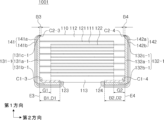
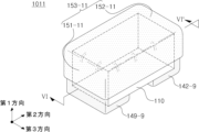
図1は、本発明の一実施形態による積層型電子部品を概略的に示した斜視図であり、図2は、図1の積層型電子部品の本体を概略的に示した斜視図であり、図3は、図1のI-I'線に沿った断面図であり、図4は、図2の本体を分解して概略的に示した分解斜視図であり、図5は、バンド電極が埋め込まれた誘電体層を示した図面であり、図6は、図3の上部を拡大して示した拡大図であり、図7は、図1の積層型電子部品が実装された基板を概略的に示した斜視図である。 FIG. 1 is a schematic perspective view of a multilayer electronic component according to an embodiment of the present invention, FIG. 2 is a schematic perspective view of the main body of the multilayer electronic component of FIG. 3 is a cross-sectional view taken along line II' of FIG. 1, FIG. 4 is an exploded perspective view schematically showing an exploded main body of FIG. 2, and FIG. 5 is a band electrode. 6 is an enlarged view showing an enlarged upper portion of FIG. 3, and FIG. 7 is a schematic diagram of a substrate on which the multilayer electronic component of FIG. 1 is mounted. 1 is a schematic perspective view. FIG.
以下、図1~図7を参照して、本発明の一実施形態による積層型電子部品1000について説明する。
A multilayer
本発明の一実施形態に係る積層型電子部品1000は、誘電体層111、上記誘電体層を間に挟んで交互に配置される第1及び第2内部電極121、122を含み、第1方向に対向する第1及び第2面1、2、上記第1及び第2面と連結され、第2方向に対向する第3及び第4面3、4、上記第1~第4面と連結され、第3方向に対向する第5及び第6面5、6を含み、上記第1面は、互いに離隔して配置される第1及び第2バンド電極123、124を含む本体110と、上記第3面に配置されて上記第1内部電極及び上記第1バンド電極と連結される第1外部電極131と、上記第4面に配置されて上記第2内部電極及び上記第2バンド電極と連結される第2外部電極132と、上記第1バンド電極上に配置される第1めっき層141と、上記第2バンド電極上に配置される第2めっき層142と、を含むことができる。
A multilayer
本体110は、誘電体層111及び内部電極121、122が交互に積層されている。
The
本体110の具体的な形状に特に制限はないが、図示のように、本体110は六面体状またはこれと類似した形状からなることができる。焼成過程で本体110に含まれたセラミック粉末の収縮によって、本体110は完全な直線を有する六面体状ではないが、実質的に六面体状を有することができる。
The specific shape of the
本体110は、第1方向に互いに対向する第1及び第2面1、2、上記第1及び第2面1、2と連結され、第2方向に互いに対向する第3及び第4面3、4、第1及び第2面1、2と連結され、第3及び第4面3、4と連結され、第3方向に互いに対向する第5及び第6面5、6を有することができる。
The
一実施形態において、本体110は、第1面と第3面を連結する第1-3コーナーC1-3、上記第1面と第4面を連結する第1-4コーナーC1-4、上記第2面と第3面を連結する第2-3コーナーC2-3、上記第2面と第4面を連結する第2-4コーナーC2-4を含み、上記第1-3コーナーC1-3及び第2-3コーナーC2-3は、上記第3面に近づくほど上記本体の第1方向の中央に収縮した形態を有し、上記第1-4コーナーC1-4及び第2-4コーナーC2-4は、上記第4面に近づくほど上記本体の第1方向の中央に収縮した形態を有することができる。
In one embodiment, the
誘電体層111上に内部電極121、122が配置されていないマージン領域が重なるにつれて、内部電極121、122の厚さによる段差が発生し、第1面と第3~第5面を連結するコーナー及び/または第2面と第3~第5面を連結するコーナーは、第1面または第2面を基準にして本体110の第1方向の中央に向かって収縮した形態を有することができる。または、本体の焼結過程での収縮挙動によって第1面1と第3~第6面3、4、5、6を連結するコーナー及び/または第2面2と第3~第6面3、4、5、6を連結するコーナーは、第1面または第2面を基準にして本体110の第1方向の中央に向かって収縮した形態を有することができる。または、チッピング不良などを防止するために、本体110の各面を連結する角を別の工程を行ってラウンド処理することで、第1面と第3~第6面を連結するコーナー及び/または第2面と第3~第6面を連結するコーナーは、ラウンド状を有することができる。
As the margin regions where the
上記コーナーは、第1面と第3面を連結する第1-3コーナー、第1面と第4面を連結する第1-4コーナー、第2面と第3面を連結する第2-3コーナー、第2面と第4面を連結する第2-4コーナーを含むことができる。また、コーナーは、第1面と第5面を連結する第1-5コーナー、第1面と第6面を連結する第1-6コーナー、第2面と第5面を連結する第2-5コーナー、第2面と第6面を連結する第2-6コーナーを含むことができる。本体110の第1~第6面は、概ね平坦な面であることができ、平坦でない領域をコーナーとして見なすことができる。以下、各面の延長線とは、各面の平坦な部分を基準に延長した線を意味することができる。
The corners are the 1-3 corner connecting the first and third surfaces, the 1-4 corner connecting the first and fourth surfaces, and the 2-3 corner connecting the second and third surfaces. The corners may include 2-4 corners connecting the 2nd and 4th faces. In addition, the corners are the 1-5 corner connecting the 1st and 5th surfaces, the 1-6 corner connecting the 1st and 6th surfaces, and the 2-5th corner connecting the 2nd and 5th surfaces. It may include 5 corners, 2-6 corners connecting the 2nd and 6th faces. The first through sixth sides of the
このとき、外部電極131、132のうち本体110のコーナー上に配置された領域をコーナー部、本体110の第3及び第4面上に配置された領域を接続部、本体の第1及び第2面上に配置された領域をバンド部とすることができる。
At this time, the regions of the
一方、内部電極121、122による段差を抑制するために、積層後に内部電極が本体の第5及び第6面5、6に露出するように切断した後、単一誘電体層または2つ以上の誘電体層を容量形成部Acの両側面に第3方向(幅方向)に積層してマージン部114、115を形成する場合には、第1面と第5及び第6面を連結する部分、及び第2面と第5及び第6面を連結する部分が収縮した形態を有しないことがある。
On the other hand, in order to suppress the step due to the
一方、本体110の第1~第6面は概ね平坦な面であることができ、平坦でない領域をコーナーとして見なすことができる。
On the other hand, the first through sixth surfaces of the
この観点から、第3及び第4コーナー部131c、132cは、上記第2面の延長線E2以下に配置されることができ、上記第3及び第4コーナー部131c、132cは、第2面と離隔して配置されることができる。すなわち、外部電極131、132が第2面上には配置されないことによって、外部電極131、132が占める体積をさらに最小化して、積層型電子部品1000の単位体積当たりの容量をさらに増加させることができる。また、第3コーナー部131cは、第3面と第2面を連結する第2-3コーナーC2-3の一部上に配置されることができ、第4コーナー部132cは、第4面と第2面を連結する第2-4コーナーC2-4の一部上に配置されることができる。
From this point of view, the third and
第2面の延長線E2は、以下のように定義されることができる。積層型電子部品1000を幅方向の中央で切断した長さ-厚さ方向の断面(L-T断面)において、第3面から第4面まで長さ方向に均等な間隔を有する厚さ方向の7つの直線P0、P1、P2、P3、P4、P5、P6、P7を引いて、P2と第2面が会う地点と、P4と第2面が会う地点を通る直線を第2面の延長線E2と定義することができる。
The extension E2 of the second surface can be defined as follows. In the length-thickness cross section (LT cross section) obtained by cutting the multilayer
一実施形態において、第1面1は、互いに離隔して配置される第1及び第2バンド電極123、124を含むことができる。
In one embodiment, the
積層型電子部品の単位体積当たりの容量を向上させて、実装空間を最小化するために実装面にのみ外部電極を配置するか、外部電極をL字状に配置した形態のMLCCが開発されている。容量及び特性の実現に不要であると判断される部分には、外部電極を配置しないことによって、追加的な有効体積を確保したものである。 In order to improve the capacity per unit volume of the multilayer electronic component and to minimize the mounting space, MLCCs have been developed in which external electrodes are arranged only on the mounting surface or external electrodes are arranged in an L shape. there is An additional effective volume is secured by not arranging the external electrodes in a portion that is judged unnecessary for realization of capacity and characteristics.
従来には、実装面に配置されるバンド電極を大きく2つの方法で形成した。第1方法は、熱処理(焼成)が終わった本体にバンド電極を形成する方法であって、別の電極焼成工程を必要とする。第2方法は、焼成前の本体上にバンド電極を印刷するか、セラミックグリーンシート上にバンド電極を印刷して本体焼成時のバンド電極も同時に熱処理する方式である。両方法とも本体の骨格が備えられた状態でバンド電極を形成するため、バンド電極による体積増加により単位体積当たりの容量を極大化することは困難であった。 Conventionally, the band electrodes arranged on the mounting surface are formed by two methods. The first method is a method of forming a band electrode on a body after heat treatment (firing), which requires another electrode firing process. The second method is to print the band electrodes on the main body before firing, or to print the band electrodes on the ceramic green sheet and heat-treat the band electrodes at the time of firing the main body at the same time. In both methods, since the band electrode is formed in a state in which the skeleton of the main body is provided, it is difficult to maximize the capacity per unit volume due to the increase in volume due to the band electrode.
ここで、本発明では、バンド電極123、124が本体110の第1面1に含まれているため、バンド電極による体積増加を抑制して単位体積当たりの容量を極大化することができる。
Here, in the present invention, since the
バンド電極123、124を形成する方法は、特に限定する必要はない。例えば、セラミックグリーンシートでバンド電極が形成される部分を除去し、上記除去された部分にバンド電極形成用ペーストを印刷した後、積層体の下部に配置して本体とともに焼成することで、バンド電極123、124を形成することができる。
A method for forming the
一実施形態において、第1バンド電極123は本体110の第3面3と連結され、第2バンド電極124は本体110の第4面3と連結されることができる。これにより、外部電極131、132との連結性を向上させることができる。また、第1バンド電極123は第1-3コーナーC1-3にも配置され、第2バンド電極124は第1-4コーナーC1-4にも配置されることができる。第1及び第2バンド電極123、124は、第5及び第6面とは離隔して配置されることができる。
In one embodiment, the
また、第1及び第2バンド電極123、124の第3方向の平均サイズは特に限定しない。例えば、第1及び第2バンド電極123、124の第3方向の平均サイズは、図2、図4及び図5に示したように、第1及び第2内部電極121、122の第3方向の平均サイズと実質的に同一であることができる。但し、これに制限されるものではなく、本体110の第3方向の平均サイズ、外部電極131、132の第3方向の平均サイズ、及び外部電極131、132との連結性を考慮して、第1及び第2バンド電極123、124の第3方向の平均サイズを決定することができる。
Also, the average size of the first and
一実施形態において、第1及び第2バンド電極123、124は、第1面に埋め込まれた形態であることができる。図5を参照すると、バンド電極123、124が含まれた誘電体層111aが第1面を形成するによって、第1及び第2バンド電極123、124は、第1面に埋め込まれた形態を有することができる。
In one embodiment, the first and
また、第1及び第2バンド電極123、124は、第1面と実質的に同一平面をなすことができる。すなわち、第1及び第2バンド電極123、124は、本体110の第1面に露出し、本体の内部に埋め込まれている形態であることができる。
Also, the first and
一実施形態において、バンド電極123、124の平均厚さtpは、0.1μm以上であることができる。バンド電極123、124が本体の内部に埋め込まれた深さをバンド電極の厚さとすることができ、バンド電極123、124の平均厚さtpは、第1方向の平均サイズを意味することができる。
In one embodiment, the average thickness tp of the
バンド電極123、124の平均厚さtpが0.1μm未満である場合には、外部電極131、132との電気的連結性を十分に確保できないか、めっき層との電気的連結性が不十分になることがある。バンド電極123、124の平均厚さtpの上限は、特に限定する必要はなく、最外層に配置された内部電極121、122及び短絡(short)を考慮して、その上限を定めることができる。
If the average thickness tp of the
バンド電極123、124の平均厚さtpは、本体110の長さ及び厚さ方向(L-T)の断面を1万倍率の走査電子顕微鏡(SEM、Scanning Electron Microscope)を用いてイメージをスキャンして測定することができ、第1面で等間隔の5つの地点で測定したバンド電極123、124の第1方向サイズを平均した値であることができる。
The average thickness tp of the
一実施形態において、第1及び第2バンド電極123、124は、Ni、Cr、Pd、及びPtのうち1つ以上を含むことができる。これにより、本体とともに焼成時の過度の収縮及び酸化を防止することができる。
In one embodiment, the first and
一実施形態において、第1及び第2バンド電極123、124は、BaTiO3、TiO2及びSiO2のうち1つ以上のセラミック添加剤を含むことができる。これにより、誘電体層との結合力を向上させ、誘電体層との焼結挙動の差を減らしてバンド電極123、124の凝集及び切れを抑制することができる。
In one embodiment, the first and
一実施形態において、第3面の延長線E3から上記第1バンド電極の端までの上記第2方向の平均サイズをD1、第4面の延長線E4から上記第2バンド電極の端までの上記第2方向の平均サイズをD2、上記第3面と上記第2内部電極が離隔した領域の第2方向の平均サイズをG1、上記第4面と上記第1内部電極が離隔した領域の第2方向の平均サイズをG2とするとき、D1≧G1及びD2≧G2を満たすことができる。これにより、基板との固着強度を向上させることができる。 In one embodiment, the average size in the second direction from the extension line E3 of the third surface to the end of the first band electrode is D1, and the average size from the extension line E4 of the fourth surface to the end of the second band electrode is D1. D2 is the average size in the second direction; G1 is the average size in the second direction of the region where the third surface and the second internal electrode are separated; Let D1≧G1 and D2≧G2 be satisfied, where G2 is the average size of the direction. Thereby, the bonding strength with the substrate can be improved.
D1及びD2は、本体110を第3方向に等間隔を有する5つの地点で第1及び第2方向に切断した断面(L-T断面)で測定した値を平均した値であることができる。
D1 and D2 may be values obtained by averaging values measured in cross sections (LT cross sections) obtained by cutting the
G1及びG2は、本体を第3方向の中央から第1及び第2方向に切断した断面において、第1方向の中央部に位置した任意の5つの第2内部電極に対して測定した第3面まで離隔した第2方向サイズを平均した値はG1とし、第1方向の中央部に位置した任意の5つの第1内部電極に対して測定した第4面まで離隔した領域の第2方向サイズを平均した値をG2とすることができる。 G1 and G2 are third planes measured with respect to arbitrary five second internal electrodes positioned at the center in the first direction in a cross section obtained by cutting the main body in the first and second directions from the center in the third direction. Let G1 be the average value of the second-direction sizes spaced apart from each other, and let G1 be the second-direction size of the region spaced from the fourth surface measured for any five first internal electrodes positioned at the center in the first direction. The averaged value can be G2.
さらに、本体110を第3方向に等間隔を有する5つの地点で第1及び第2方向に切断した断面(L-T断面)でG1及びG2を求め、それらを平均した値をG1及びG2としてさらに一般化することができる。
Furthermore, G1 and G2 are obtained in cross sections (LT cross sections) obtained by cutting the
一実施形態において、本体110の第2方向の平均サイズをL、第3面の延長線E3から上記第1バンド電極の端までの上記第2方向の平均サイズをD1、第4面の延長線E4から上記第2バンド電極の端までの上記第2方向の平均サイズをD2とするとき、0.2≦D1/L≦0.4及び0.2≦D2/L≦0.4を満たすことができる。
In one embodiment, L is the average size of the
D1/L及びD2/Lが0.2未満である場合には、十分な固着強度を確保し難いことがある。一方、D2/Lが0.4超過である場合には、高圧電流下で第1バンド電極123と第2バンド電極124との間で漏れ電流が発生するおそれがあり、めっき工程時にめっき拡散などによって第1バンド電極123と第2バンド電極124が電気的に連結されるおそれがある。
When D1/L and D2/L are less than 0.2, it may be difficult to ensure sufficient fixing strength. On the other hand, if D2/L exceeds 0.4, leakage current may occur between the
D1、D2及びLは、本体110を第3方向に等間隔を有する5つの地点で第1及び第2方向に切断した断面(L-T断面)で測定した値を平均した値であることができる。
D1, D2, and L are average values of values measured in cross sections (LT cross sections) obtained by cutting the
本体110を形成する複数の誘電体層111は焼成された状態であり、隣接する誘電体層111間の境界は走査電子顕微鏡(SEM:Scanning Electron Microscope)を利用せずには確認しにくいほど一体化することができる。
The plurality of
本発明の一実施形態によると、上記誘電体層111を形成する原料は、十分な静電容量を得ることができる限り特に制限されない。例えば、チタン酸バリウム系材料、鉛複合ペロブスカイト系材料、またはチタン酸ストロンチウム系材料などを用いることができる。上記チタン酸バリウム系材料は、BaTiO3系セラミック粉末を含むことができ、上記セラミック粉末の例示として、BaTiO3、BaTiO3にCa(カルシウム)、Zr(ジルコニウム)などが一部固溶された(Ba1-xCax)TiO3(0<x<1)、Ba(Ti1-yCay)O3(0<y<1)、(Ba1-xCax)(Ti1-yZry)O3(0<x<1、0<y<1)またはBa(Ti1-yZry)O3(0<y<1)などが挙げられる。
According to one embodiment of the present invention, the material for forming the
また、上記誘電体層111を形成する原料は、チタン酸バリウム(BaTiO3)などのパウダーに本発明の目的に応じて様々なセラミック添加剤、有機溶剤、結合剤、分散剤などが添加されることができる。
In addition, the raw material for forming the
一方、誘電体層111の平均厚さtdは特に限定する必要はない。
On the other hand, the average thickness td of the
但し、積層型電子部品の小型化及び高容量化をより容易に達成するために、誘電体層111の平均厚さtdは0.35μm以下であることができる。
However, the average thickness td of the
また、本発明の一実施形態によって外部電極上に絶縁層を配置する場合、外部からの水分浸透、めっき液の浸透などを防止して信頼性を向上させることができるため、誘電体層111の平均厚さtdが0.35μm以下である場合にも優れた信頼性を確保することができる。したがって、誘電体層111の平均厚さtdが0.35μm以下である場合に、本発明による信頼性向上の効果がより顕著になることができる。
In addition, when the insulating layer is disposed on the external electrode according to an embodiment of the present invention, it is possible to prevent permeation of moisture and plating solution from the outside, thereby improving reliability. Excellent reliability can be ensured even when the average thickness td is 0.35 μm or less. Therefore, when the average thickness td of the
上記誘電体層111の平均厚さtdは、上記第1及び第2内部電極121、122の間に配置される誘電体層111の平均厚さを意味することができる。
The average thickness td of the
誘電体層111の平均厚さは、本体110の長さ及び厚さ方向(L-T)の断面を1万倍率の走査電子顕微鏡(SEM、Scanning Electron Microscope)を用いてイメージをスキャンして測定することができる。より具体的には、スキャンされたイメージから1つの誘電体層を長さ方向に等間隔である30つの地点でその厚さを測定して平均値を測定することができる。上記等間隔である30つの地点は、容量形成部Acで指定されることができる。また、このような平均値測定を10つの誘電体層に拡張して平均値を測定すると、誘電体層の平均厚さをさらに一般化することができる。
The average thickness of the
本体110は、本体110の内部に配置され、誘電体層111を間に挟んで互いに向かい合うように配置される第1内部電極121及び第2内部電極122を含んで容量が形成される容量形成部Acと、上記容量形成部Acの第1方向の上部及び下部に形成されたカバー部112、113を含むことができる。
The
また、上記容量形成部Acは、キャパシタの容量形成に寄与する部分であって、誘電体層111を間に挟んで複数の第1及び第2内部電極121、122を繰り返し積層して形成されることができる。
The capacitance forming portion Ac is a portion that contributes to the capacitance formation of the capacitor, and is formed by repeatedly laminating a plurality of first and second
カバー部112、113は、上記容量形成部Acの第1方向の上部に配置される上部カバー部112及び上記容量形成部Acの第1方向の下部に配置される下部カバー部113を含むことができる。下部カバー部113は、第1及び第2バンド電極123、124を含むことができる。上部カバー部112は、第3及び第4バンド電極125、126を含むことができる。
The
図4を参照すると、上記上部カバー部112及び下部カバー部113は、単一誘電体層または2つ以上の誘電体層を容量形成部Acの上下面にそれぞれ厚さ方向に積層し、最外層にはバンド電極123、124が含まれた誘電体層111aを1つ以上積層して形成することができる。カバー部112、113は、基本的に物理的または化学的ストレスによる内部電極の損傷を防止する役割を果たすことができる。
Referring to FIG. 4, the
上記上部カバー部112及び下部カバー部113は、バンド電極123、124は含むことができるが、内部電極121、122は含まず、誘電体層111と同一材料を含むことができる。すなわち、上記上部カバー部112及び下部カバー部113は、セラミック材料を含むことができ、例えば、チタン酸バリウム(BaTiO3)系セラミック材料を含むことができる。
The
一方、カバー部112、113の平均厚さは特に限定する必要はない。但し、積層型電子部品の小型化及び高容量化をより容易に達成するために、カバー部112、113の平均厚さtcは15μm以下であることができる。また、本発明の一実施形態によって外部電極上に絶縁層を配置する場合、外部からの水分浸透、めっき液の浸透などを防止して信頼性を向上させることができるため、カバー部112、113の平均厚さtcが15μm以下である場合にも優れた信頼性を確保することができる。
On the other hand, the average thickness of the
カバー部112、113の平均厚さtcは、第1方向の平均サイズを意味することができ、容量形成部Acの上部または下部で等間隔の5つの地点で測定したカバー部112、113の第1方向サイズを平均した値であることができる。
The average thickness tc of the
また、上記容量形成部Acの側面には、マージン部114、115が配置されることができる。
In addition,
マージン部114、115は、本体110の第5面5に配置されたマージン部114及び第6面6に配置されたマージン部115を含むことができる。すなわち、マージン部114、115は、上記本体110の幅方向の両端面(end surfaces)に配置されることができる。
The
マージン部114、115は、図3に示したように、上記本体110を幅-厚さ(W-T)方向に切った断面(cross-section)において、第1及び第2内部電極121、122の両端と本体110の境界面との間の領域を意味することができる。
As shown in FIG. 3, the
マージン部114、115は、基本的に物理的または化学的ストレスによる内部電極の損傷を防止する役割を果たすことができる。
The
マージン部114、115は、セラミックグリーンシート上にマージン部が形成されるところを除き、導電性ペーストを塗布して内部電極を形成することで形成されたものであることができる。
The
また、内部電極121、122による段差を抑制するために、積層後に内部電極が本体の第5及び第6面5、6に露出するように切断した後、単一誘電体層または2つ以上の誘電体層を容量形成部Acの両側面に第3方向(幅方向)に積層してマージン部114、115を形成することもできる。
In addition, in order to suppress a step due to the
一方、マージン部114、115の平均幅は特に限定する必要はない。但し、積層型電子部品の小型化及び高容量化をより容易に達成するために、マージン部114、115の平均幅は15μm以下であることができる。また、本発明の一実施形態によって外部電極上に絶縁層を配置する場合、外部からの水分浸透、めっき液の浸透などを防止して信頼性を向上させることができるため、マージン部114、115の平均幅が0.35μm以下である場合にも優れた信頼性を確保することができる。
On the other hand, the average width of the
マージン部114、115の平均幅は、第3方向の平均サイズを意味することができ、容量形成部Acの側面で等間隔の5つの地点で測定したマージン部114、115の第3方向のサイズを平均した値であることができる。
The average width of the
内部電極121、122は誘電体層111と交互に積層される。
The
内部電極121、122は、第1及び第2内部電極121、122を含むことができる。第1及び第2内部電極121、122は、本体110を構成する誘電体層111を間に挟んで互いに対向するように交互に配置され、本体110の第3及び第4面3、4にそれぞれ露出することができる。
The
図3を参照すると、第1内部電極121は第4面4と離隔し、第3面3を介して露出し、第2内部電極122は第3面3と離隔し、第4面4を介して露出することができる。本体の第3面3には、第1外部電極131が配置されて第1内部電極121と連結され、本体の第4面4には、第2外部電極132が配置されて第2内部電極122と連結されることができる。
Referring to FIG. 3 , the first
すなわち、第1内部電極121は第2外部電極132とは連結されずに第1外部電極131と連結され、第2内部電極122は第1外部電極131とは連結されずに第2外部電極132と連結される。したがって、第1内部電極121は第4面4で一定距離離隔して形成され、第2内部電極122は第3面3で一定距離離隔して形成されることができる。
That is, the first
このとき、第1及び第2内部電極121、122は、中間に配置された誘電体層111によって互いに電気的に分離することができる。
At this time, the first and second
本体110は、第1内部電極121が印刷されたセラミックグリーンシートと第2内部電極122が印刷されたセラミックグリーンシートを交互に積層した後、焼成して形成することができる。
The
内部電極121、122を形成する材料は特に制限されず、電気導電性に優れた材料を用いることができる。例えば、内部電極121、122は、ニッケル(Ni)、銅(Cu)、パラジウム(Pd)、銀(Ag)、金(Au)、白金(Pt)、スズ(Sn)、タングステン(W)、チタン(Ti)、及びこれらの合金のうち1つ以上を含むことができる。
Materials for forming the
また、内部電極121、122は、ニッケル(Ni)、銅(Cu)、パラジウム(Pd)、銀(Ag)、金(Au)、白金(Pt)、スズ(Sn)、タングステン(W)、チタン(Ti)及びこれらの合金のうち1つ以上を含む内部電極用導電性ペーストをセラミックグリーンシートに印刷して形成することができる。上記内部電極用導電性ペーストの印刷方法は、スクリーン印刷法またはグラビア印刷法などを用いることができ、本発明がこれに限定されるものではない。
The
一方、内部電極121、122の平均厚さteは特に限定する必要はない。
On the other hand, the average thickness te of the
積層型電子部品の小型化及び高容量化をより容易に達成するために、内部電極121、122の平均厚さteは0.35μm以下であることができる。
The average thickness te of the
また、本発明の一実施形態によって外部電極上に絶縁層を配置する場合、外部からの水分浸透、めっき液の浸透などを防止して信頼性を向上させることができるため、内部電極121、122の平均厚さが0.35μm以下である場合にも優れた信頼性を確保することができる。したがって、内部電極121、122の平均厚さが0.35μm以下である場合に、本発明による効果がより顕著になり、積層型電子部品の小型化及び高容量化をより容易に達成することができる。
In addition, when an insulating layer is disposed on the external electrodes according to an embodiment of the present invention, the
内部電極121、122の平均厚さは、本体110の長さ及び厚さ方向(L-T)の断面を1万倍率の走査電子顕微鏡(SEM、Scanning Electron Microscope)を用いてイメージをスキャンして測定することができる。より具体的には、スキャンされたイメージから1つの内部電極を長さ方向に等間隔である30つの地点でその厚さを測定して平均値を測定することができる。上記等間隔である30つの地点は、容量形成部Acで指定されることができる。また、このような平均値測定を10つの内部電極に拡張して平均値を測定すると、内部電極の平均厚さをさらに一般化することができる。
The average thickness of the
外部電極131、132は、本体110の第3面3及び第4面4に配置されることができる。外部電極131、132は、本体110の第3及び第4面3、4にそれぞれ配置され、第1及び第2内部電極121、122とそれぞれ連結された第1及び第2外部電極131、132を含むことができる。また、第1及び第2外部電極131、132は、第1及び第2バンド電極123、124とそれぞれ連結されることができる。
The
一実施形態において、第1及び第2外部電極131、132は、第1及び第2面と離隔して配置されることができる。一実施形態において、第1及び第2外部電極131、132は、第5及び第6面と離隔して配置されることができる。また、第1及び第2外部電極131、132は、第1、第2、第5及び第6面と離隔して配置されることができる。すなわち、第1及び第2外部電極131、132は、第1、第2、第5及び第6面には配置されないことができる。これによって、外部電極131、132が占める体積を最小化して積層型電子部品1000の単位体積当たりの容量を増加させることができる。
In one embodiment, the first and second
外部電極131、132は、本体110のコーナーに延びてコーナー上に配置されたコーナー部を含むことができる。すなわち、一実施形態において、第1外部電極131は、上記第3面に配置される第1接続部131a、上記第1接続部131aから上記第1面と第3面を連結するコーナーに延びて配置される第1コーナー部131b、及び上記第1接続部131aから上記第2面と第3面を連結するコーナーに延びて配置される第3コーナー部131cを含むことができる。これにより、外部電極とバンド電極との連結性を向上させながらも単位体積当たりの容量を極大化することができる。第1及び第2コーナー部131b、132bは、第1面の延長線E1と会わないように配置することができ、第3及び第4コーナー部131c、132cは、第2面の延長線E2以下に配置されることができる。すなわち、第1及び第2コーナー部131b、132bは第1面には配置されず、第3及び第4コーナー部131c、132cは第2面には配置されないことがある。
The
このとき、第3面の延長線E3から上記第1コーナー部131bの端までの上記第2方向の平均サイズをB1、上記第4面の延長線E4から上記第2コーナー部132bの端までの上記第2方向の平均サイズをB2、上記第3面の延長線から上記第3コーナー部131cの端までの上記第2方向の平均サイズをB3、上記第4面の延長線から上記第4コーナー部132cの端までの上記第2方向の平均サイズをB4、上記第3面と第2内部電極122が離隔した領域の第2方向の平均サイズをG1、上記第4面と第1内部電極121が離隔した領域の第2方向の平均サイズをG2とするとき、B1≦G1、B3≦G1、B2≦G2及びB4≦G2を満たすことができる。これにより、外部電極131、132が占める体積を最小化して積層型電子部品1000の単位体積当たりの容量を増加させることができる。
At this time, the average size in the second direction from the extension line E3 of the third surface to the end of the
B1、B2、B3及びB4は、本体110を第3方向に等間隔を有する5つの地点で第1及び第2方向に切断した断面(L-T断面)で測定した値を平均した値であることができる。
B1, B2, B3, and B4 are the average values measured in cross sections (LT cross sections) obtained by cutting the
G1及びG2は、本体を第3方向の中央から第1及び第2方向に切断した断面において、第1方向の中央部に位置した任意の5つの第2内部電極に対して測定した第3面まで離隔した第2方向サイズを平均した値はG1とし、第1方向の中央部に位置した任意の5つの第1内部電極に対して測定した第4面まで離隔した領域の第2方向サイズを平均した値をG2とすることができる。 G1 and G2 are third planes measured with respect to arbitrary five second internal electrodes positioned at the center in the first direction in a cross section obtained by cutting the main body in the first and second directions from the center in the third direction. Let G1 be the average value of the second-direction sizes spaced apart from each other, and let G1 be the second-direction size of the region spaced from the fourth surface measured for any five first internal electrodes positioned at the center in the first direction. The averaged value can be G2.
さらに、本体110を第3方向に等間隔を有する5つの地点で第1及び第2方向に切断した断面(L-T断面)でG1及びG2を求め、それらを平均した値をG1及びG2として、さらに一般化することができる。
Furthermore, G1 and G2 are obtained in cross sections (LT cross sections) obtained by cutting the
但し、これに制限されず、後述するように外部電極131、132は、第1面及び第2面の一部に延びるバンド部を含むことができる。さらに、第1外部電極131は、第1接続部131aから第5及び第6面の一部まで延びる側面バンド部を含むこともでき、第2外部電極132は、第2接続部132aから第5及び第6面の一部まで延びる側面バンド部を含むことができる。
However, the
本実施形態では、積層型電子部品1000が2つの外部電極131、132を有する構造を説明しているが、外部電極131、132の個数や形状などは内部電極121、122の形態やその他の目的に応じて変わることができる。
In this embodiment, a structure in which the multilayer
一方、外部電極131、132は、金属などのように電気導電性を有するものであれば、如何なる物質を用いても形成することができ、電気的特性、構造的安定性などを考慮して具体的な物質が決定されることができ、さらに多層構造を有することができる。
On the other hand, the
外部電極131、132は、導電性金属及びガラスを含む焼成(firing)電極であるか、導電性金属及び樹脂を含む樹脂系電極であることができる。
The
なお、外部電極131、132は、本体上に焼成電極及び樹脂系電極が順次形成された形態であることができる。また、外部電極131、132は、本体上に導電性金属を含むシートを転写する方式で形成されるか、焼成電極上に導電性金属を含むシートを転写する方式で形成されたものであることができる。
In addition, the
外部電極131、132に含まれる導電性金属として、電気導電性に優れた材料を用いることができ、特に限定しない。例えば、導電性金属は、Cu、Ni、Pd、Ag、Sn、Cr及びそれらの合金のうち1つ以上であることができる。好ましくは、外部電極131、132は、Ni及びNi合金のうち1つ以上を含むことができ、これによって、Niを含む内部電極121、122との連結性をより向上させることができる。
As the conductive metal contained in the
また、外部電極131、132がCuを含むことができ、これによって、バンド電極123、124との結合力を向上させることができ、内部電極121、122との電気的連結性もより向上させることができる。
In addition, the
第1及び第2めっき層141、142は、それぞれ第1及び第2バンド電極123、124上に配置されることができる。第1及び第2めっき層141、142は、それぞれ第1及び第2バンド電極123、124と直接接するように配置されることができる。めっき層141、142は、実装特性を向上させる役割を果たすことができる。
The first and second plating layers 141, 142 can be disposed on the first and
また、第1めっき層141は、第1バンド電極123及び第1外部電極131上に配置されることができ、第2めっき層142は、第2バンド電極124及び第2外部電極132上に配置されることができる。また、第1めっき層141は、第1バンド電極123及び第1外部電極131を覆うように配置されることができ、第2めっき層142は、第2バンド電極124及び第2外部電極132を覆うように配置されることができる。
Also, the
めっき層141、142の種類は特に限定されず、Cu、Ni、Sn、Ag、Au、Pd及びこれらの合金のうち1つ以上を含むめっき層であることができ、複数層で形成されることができる。 The types of the plating layers 141 and 142 are not particularly limited, and may be plating layers containing one or more of Cu, Ni, Sn, Ag, Au, Pd, and alloys thereof, and may be formed of multiple layers. can be done.
めっき層141、142に対するより具体的な例を挙げると、めっき層141、142は、Niめっき層141a、142a及びSnめっき層141b、142bが順次配置された形態であることができる。
As a more specific example of the plating layers 141 and 142, the plating layers 141 and 142 may have a form in which
積層型電子部品1000が実装された実装基板1100を示した図7を参照すると、積層型電子部品1000のめっき層141、142は、基板180上に配置された電極パッド181、182及びはんだ191、192によって接合されることができる。
Referring to FIG. 7 showing a mounting
一方、内部電極121、122が第1方向に積層されている場合には、内部電極121、122が実装面と平行するように積層型電子部品1000を基板180に水平実装することができる。但し、本発明が水平実装である場合に限定されるものではなく、内部電極121、122を第3方向に積層する場合には、内部電極121、122が実装面と垂直になるように、基板に積層型電子部品を垂直実装することができる。
On the other hand, when the
積層型電子部品1000のサイズは特に限定する必要はない。
The size of the multilayer
但し、小型化及び高容量化を同時に達成するためには、誘電体層及び内部電極の厚さを薄くして、積層数を増加させる必要があるため、1005(長さ×幅、1.0mm×0.5mm)以下のサイズを有する積層型電子部品1000において本発明による信頼性及び単位体積当たりの容量向上の効果がより顕著になることができる。 However, in order to achieve both miniaturization and high capacity at the same time, it is necessary to reduce the thickness of the dielectric layers and internal electrodes and increase the number of laminated layers. × 0.5 mm) or less, the effect of improving reliability and capacity per unit volume according to the present invention can be more pronounced.
したがって、製造誤差、外部電極サイズなどを考慮すると、積層型電子部品1000の長さが1.1mm以下であり、幅が0.55mm以下である場合、本発明による信頼性向上の効果がより顕著になることができる。ここで、積層型電子部品1000の長さは積層型電子部品1000の第2方向サイズを意味し、積層型電子部品1000の幅は積層型電子部品1000の第3方向サイズを意味することができる。
Therefore, considering manufacturing errors, external electrode sizes, etc., when the multilayer
図8は、図3の変形例を示した図面である。 FIG. 8 is a drawing showing a modification of FIG.
図8を参照すると、積層型電子部品1001は、第1バンド部131b-1を含む第1外部電極131-1及び第2バンド部132b-1を含む第2外部電極132-1を含むことができる。
Referring to FIG. 8, the multilayer
第1外部電極131-1は、第3面に配置される第1接続部131a-1、上記第1接続部から上記第1面の一部まで延びて配置される第1バンド部131b-1、及び上記第1接続部から上記第2面と第3面を連結するコーナーに延びて配置される第3コーナー部131c-1を含み、第2外部電極132-1は上記第4面に配置される第2接続部132a-1、上記第2接続部から上記第1面の一部まで延びて配置される第2バンド部132b-1、及び上記第2接続部から第2面と第4面を連結するコーナーに延びて配置される第4コーナー部132c-1を含むことができる。
The first external electrode 131-1 includes a first connecting
一実施形態において、第3面の延長線E3から上記第1バンド部131b-1の端までの上記第2方向の平均サイズをB1、第4面E4の延長線から上記第2バンド部132b-1の端までの上記第2方向の平均サイズをB2、上記第3面の延長線から上記第3コーナー部131c-1の端までの上記第2方向の平均サイズをB3、上記第4面の延長線から上記第4コーナー部132c-1の端までの上記第2方向の平均サイズをB4、上記第3面と上記第2内部電極が離隔した領域の第2方向の平均サイズをG1、上記第4面と上記第1内部電極が離隔した領域の第2方向の平均サイズをG2とするとき、B1≧G1、B3≦G1、B2≧G2及びB4≦G2を満たすことができる。B1≧G1及びB2≧G2を満たすことにより、バンド電極123、124と外部電極131-1、132-1との間の電気的連結性をより向上させることができ、B3≦G1及びB4≦G2を満たすことによって、外部電極131-1、132-1が占める体積を減らすことができる。
In one embodiment, the average size in the second direction from the extension line E3 of the third surface to the end of the
B1、B2、B3及びB4は、本体110を第3方向に等間隔を有する5つの地点で第1及び第2方向に切断した断面(L-T断面)で測定した値を平均した値であることができる。
B1, B2, B3, and B4 are the average values measured in cross sections (LT cross sections) obtained by cutting the
G1及びG2は、本体を第3方向の中央から第1及び第2方向に切断した断面において、第1方向の中央部に位置した任意の5つの第2内部電極に対して測定した第3面まで離隔した第2方向サイズを平均した値はG1とし、第1方向の中央部に位置した任意の5つの第1内部電極に対して測定した第4面まで離隔した領域の第2方向サイズを平均した値をG2とすることができる。 G1 and G2 are third planes measured with respect to arbitrary five second internal electrodes positioned at the center in the first direction in a cross section obtained by cutting the main body in the first and second directions from the center in the third direction. Let G1 be the average value of the second-direction sizes spaced apart from each other, and let G1 be the second-direction size of the region spaced from the fourth surface measured for any five first internal electrodes positioned at the center in the first direction. The averaged value can be G2.
さらに、本体110を第3方向に等間隔を有する5つの地点で第1及び第2方向に切断した断面(L-T断面)でG1及びG2を求め、それらを平均した値をG1及びG2として、さらに一般化することができる。
Furthermore, G1 and G2 are obtained in cross sections (LT cross sections) obtained by cutting the
また、第1バンド部131b-1の端は、第1バンド電極123の端を覆うように配置されることができ、第2バンド部132b-1の端は、第1バンド電極124の端を覆うように配置されることができる。すなわち、第3面の延長線E3から上記第1バンド電極の端までの上記第2方向の平均サイズをD1、第4面の延長線E4から上記第2バンド電極の端までの上記第2方向の平均サイズをD2とするとき、B1≧D1及びB2≧D2を満たすことができる。
Also, the end of the
D1及びD2は、本体110を第3方向に等間隔を有する5つの地点で第1及び第2方向に切断した断面(L-T断面)で測定した値を平均した値であることができる。
D1 and D2 may be values obtained by averaging values measured in cross sections (LT cross sections) obtained by cutting the
図9は、本発明の一実施形態による積層型電子部品1002を概略的に示した斜視図であり、図10は、図9のII-II'線に沿った断面図である。
FIG. 9 is a schematic perspective view of a multilayer
本発明の一実施形態による積層型電子部品1002は、外部電極131、132上に配置された絶縁層151、152を含むことができる。
A multilayer
第1及び第2絶縁層151、152は、それぞれ第1及び第2外部電極131、132上に配置されることができる。
First and second insulating
第1及び第2外部電極131、132は内部電極121、122と連結される部位であるため、めっき工程でめっき液の浸透または実使用時の水分浸透の経路となり得る。本発明の一実施形態においては、外部電極131、132上に絶縁層151、152が配置されるため、外部からの水分浸透またはめっき液の浸透を防止することができ、外部電極131、132のうち、絶縁層151、152が配置された領域には、めっき層141-2、142-2が配置されることを防止することができる。
Since the first and second
第1及び第2絶縁層151、152を形成する材料は特に限定されない。例えば、第1及び第2絶縁層151、152はガラスを含むか、高分子樹脂を含むことができる。上記高分子樹脂の種類は特に限定する必要はない。例えば、上記高分子樹脂は、エポキシ樹脂、アクリル樹脂、エチルセルロース(Ethyl Cellulose)などから選択された1種以上であることができる。
Materials for forming the first and second insulating
一実施形態において、絶縁層151、152が高分子樹脂を含む場合、TiO2、BaTiO3、Al2O3、SiO2、BaOなどから選択された1種以上を添加剤として含むことができる。これにより、本体または外部電極との結合力を向上させることができる。
In one embodiment, when the insulating
絶縁層151、152を形成する方法は、特に制限する必要はないが、例えば、ペーストを外部電極131、132上に塗布するか、シートを外部電極131、132上に転写する方式で形成することができる。
The method of forming the insulating
絶縁層151、152の平均厚さは、特に限定しないが、例えば、3~30μmであることができる。ここで、絶縁層151、152の平均厚さとは、接続部131a、132a上の等間隔の5つの地点で測定した絶縁層151、152の第2サイズを平均した値を意味することができる。
The average thickness of the insulating
第1及び第2めっき層141-2、142-2は、第1及び第2バンド電極123、124上に配置されることができる。第1及び第2めっき層141-2、142-2は、実装特性を向上させる役割を果たす。第1及び第2めっき層141-2、142-2の種類は特に限定されず、Ni、Sn、Pd及びこれらの合金のうち1つ以上を含むめっき層であることができ、複数層で形成されることができる。
First and second plating layers 141-2, 142-2 may be disposed on the first and
第1及び第2めっき層141-2、142-2に対するより具体的な例を挙げると、第1及び第2めっき層141-2、142-2は、第1及び第2バンド電極123、124上にNiめっき層141-2a及びSnめっき層141-2bが順次形成された形態であることができる。
To give a more specific example of the first and second plating layers 141-2, 142-2, the first and second plating layers 141-2, 142-2 are the first and
一実施形態において、第1及び第2めっき層141-2、142-2は、それぞれ第1及び第2外部電極131、132を一部覆うように延びて配置されることができる。
In one embodiment, the first and second plating layers 141-2 and 142-2 may be extended to partially cover the first and second
第1面1から第1及び第2内部電極121、122のうち、第1面1の最も近くに配置された内部電極までの第1方向の平均サイズをH1、上記第1面1の延長線から上記第1及び第2外部電極131、132上に配置された第1及び第2めっき層141-2、142-2の端までの第1方向の平均サイズをH2とするとき、H1>H2(またはH1≧H2)を満たすことができる。これにより、めっき工程時にめっき液が内部電極に浸透することを抑制して信頼性を向上させることができる。
H1 is the average size in the first direction from the
H1及びH2は、本体110を第3方向に等間隔を有する5つの地点で第1及び第2方向に切断した断面(L-T断面)で測定した値を平均した値であることができる。H1は各断面において、第1面1の最も近くに配置された内部電極が外部電極と連結される地点で測定した値を平均した値であることができ、H2は各断面において、外部電極と接するめっき層の端を基準に測定した値を平均した値であることができ、H1及びH2の測定時に基準となる第1面の延長線は同一であることができる。
H1 and H2 may be values obtained by averaging values measured in cross sections (LT cross sections) obtained by cutting the
一実施形態において、第1及び第2絶縁層251、252は、第1及び第2外部電極131、132とそれぞれ直接接するように配置され、第1及び第2外部電極131、132は、導電性金属及びガラスを含むことができる。これにより、第1及び第2外部電極131、132の外表面のうち絶縁層251、252が配置された領域には、めっき層141-2、142-2が配置されないことがあるため、めっき液による外部電極の侵食を効果的に防止することができる。
In one embodiment, the first and second insulating layers 251, 252 are disposed in direct contact with the first and second
一実施形態において、第1めっき層141-2は、第1絶縁層151の第1外部電極131上に配置された端を覆うように配置され、第2めっき層142-2は、第2絶縁層152の第2外部電極132上に配置された端を覆うように配置されることができる。これにより、絶縁層151、152とめっき層141-2、142-2との結合力を強化して積層型電子部品1002の信頼性を向上させることができる。また、外部電極131、132上にめっき層141-2、142-2を形成する前に第1及び第2絶縁層151、152を先に形成することで、めっき層の形成過程におけるめっき液の浸透をより確実に抑制することができる。めっき層よりも絶縁層を先に形成することによって、めっき層141-2、142-2が絶縁層151、152の端を覆う形態を有することができる。
In one embodiment, the first plating layer 141-2 is disposed to cover the edge of the
一実施形態において、第1絶縁層151は、第1めっき層141-2の第1外部電極231上に配置された端を覆うように配置され、第2絶縁層152は、第2めっき層141-2の第2外部電極132上に配置された端を覆うように配置されることができる。これにより、絶縁層151、152とめっき層141-2、142-2の結合力を強化して積層型電子部品1002の信頼性を向上させることができる。
In one embodiment, the first insulating
図11は、図9の変形例を示したものである。図11を参照すると、本発明の一実施形態による積層型電子部品1002の変形例1003は、第1及び第2絶縁層151-3、152-3が第5及び第6面5、6に延びて互いに連結されることで、1つの絶縁層153-3と連結されることができる。このとき、連結された第1及び第2絶縁層153-3が第5面及び第6面の一部を覆うように配置されることができる。
FIG. 11 shows a modification of FIG. Referring to FIG. 11, a
図12は、本発明の一実施形態による積層型電子部品1004を概略的に示した斜視図であり、図13は、図12のIII-III'線に沿った断面図である。
FIG. 12 is a schematic perspective view of a multilayer
図12及び図13を参照すると、本発明の一実施形態による積層型電子部品1004は、第1及び第2めっき層141-4、142-4が第1面の延長線E1以下に配置されることができる。これにより、実装時にはんだの高さを最小化することができ、実装区間を最小化することができる。このとき、外部電極131、132とめっき層141-4、141-5は直接接触しないことがある。
Referring to FIGS. 12 and 13, in a multilayer
また、第1及び第2絶縁層151-4、152-4は、第1面の延長線以下まで延びて第1及び第2めっき層141-4、142-4と接するように配置されることができる。 Also, the first and second insulating layers 151-4 and 152-4 are arranged to extend below the extension line of the first surface and contact the first and second plating layers 141-4 and 142-4. can be done.
図14は、図13の変形例を示した図面である。図14を参照すると、図13の変形例による積層型電子部品1005は、めっき層141-5、142-5が2層形態ではなく、1層形態で配置されることができる。これにより、単位体積当たりの容量向上の効果をより向上させることができる。このとき、めっき層141-5、142-5は、Snめっき層であることができる。
14 is a drawing showing a modification of FIG. 13. FIG. Referring to FIG. 14, in the multilayer
図15は、図12の変形例を示したものである。図12を参照すると、本発明の一実施形態による積層型電子部品1004の変形例1006は、第1及び第2絶縁層151-6、152-6が第5及び第6面5、6に延びて互いに連結されることで、1つの絶縁層153-6と連結されることができる。このとき、連結された第1及び第2絶縁層153-6が第5面及び第6面の全部を覆うように配置されることができる。
FIG. 15 shows a modification of FIG. Referring to FIG. 12, a
図16は、本発明の一実施形態による積層型電子部品1007を概略的に示した斜視図であり、図17は、図16のIV-IV'線に沿った断面図である。
FIG. 16 is a schematic perspective view of a multilayer
図16及び図17を参照すると、本発明の一実施形態による積層型電子部品1007は、第1面1上に配置され、第1めっき層141-4と第2めっき層142-4との間に配置される追加絶縁層161をさらに含むことができる。これにより、高圧電流下で第1バンド電極123と第2バンド電極124との間で発生し得る漏れ電流などを防止することができる。
16 and 17, the multilayer
追加絶縁層161の種類は特に限定する必要はない。例えば、追加絶縁層161はガラスを含むか、高分子樹脂を含むことができる。上記高分子樹脂の種類は特に限定する必要はない。例えば、上記高分子樹脂は、エポキシ樹脂、アクリル樹脂、エチルセルロース(Ethyl Cellulose)などから選択された1種以上であることができる。一実施形態において、追加絶縁層161が高分子樹脂を含む場合、TiO2、BaTiO3、Al2O3、SiO2、BaOなどから選択された1種以上を添加剤として含むことができる。これにより、本体または外部電極との結合力を向上させることができる。
The type of additional insulating
一方、追加絶縁層161及び絶縁層151-7、152-7が同一材料から形成される必要はなく、相違する材料から形成されることができる。
On the other hand, the additional insulating
図18は、図16の変形例を示したものである。図18を参照すると、本発明の一実施形態による積層型電子部品1007の変形例1008は、第1及び第2絶縁層151-8、152-8が第5及び第6面5、6に延びて互いに連結されることで、1つの絶縁層153-8に連結されることができる。
FIG. 18 shows a modification of FIG. Referring to FIG. 18, a
図19は、本発明の一実施形態による積層型電子部品1009を概略的に示した斜視図であり、図20は、図19のV-V'線に沿った断面図である。
FIG. 19 is a schematic perspective view of a multilayer
図19及び図20を参照すると、一実施形態による積層型電子部品1009は、第1外部電極131上に配置される第1絶縁層151-9、第2外部電極132上に配置される第2絶縁層152-9を含み、第1面1から上記第1及び第2内部電極121、122のうち、上記第1面1の最も近くに配置された内部電極までの第1方向の平均サイズをH1、上記第1面1の延長線から上記第1及び第2外部電極131、132上に配置されためっき層141-9、142-9の端までの第1方向の平均サイズをH2とするとき、H1<H2を満たすことができる。これによって、実装時にはんだと接する面積を増加させて固着強度を向上させることができる。
19 and 20, the multilayer
より好ましくは、本体110の第1方向の平均サイズをTとするとき、H2<T/2を満たすことができる。すなわち、H1<H2<T/2を満たすことができる。H2がT/2以上の場合には、絶縁層による耐湿信頼性向上の効果が低下するおそれがあるためである。
More preferably, H2<T/2, where T is the average size of the
H1、H2及びTは、本体110を第3方向に等間隔を有する5つの地点で第1及び第2方向に切断した断面(L-T断面)で測定した値を平均した値であることができる。H1は各断面において、第1面1の最も近くに配置された内部電極が外部電極と連結される地点で測定した値を平均した値であることができ、H2は各断面において、外部電極と接するめっき層の端を基準に測定した値を平均した値であることができ、H1及びH2の測定時に基準となる第1面の延長線は同一であることができる。また、Tは、各断面において、本体110の第1方向の最大サイズを測定した後の平均値であることができる。
H1, H2 and T are average values of values measured in cross sections (LT cross sections) obtained by cutting the
図21は、図19の変形例を示したものである。図21を参照すると、本発明の一実施形態による積層型電子部品1009の変形例1010は、第1及び第2絶縁層151-10、152-10が第5及び第6面5、6に延びて互いに連結されることで、1つの絶縁層153-10に連結されることができる。
FIG. 21 shows a modification of FIG. Referring to FIG. 21, a
図22は、本発明の一実施形態による積層型電子部品1011を概略的に示した斜視図であり、図23は、図22のVI-VI'線に沿った断面図である。
FIG. 22 is a schematic perspective view of a multilayer
図22及び図23を参照すると、本発明の一実施形態による積層型電子部品1011は、第1及び第2絶縁層151-11、152-11が第2、第5及び第6面2、5、6に延びて互いに連結されることで、1つの絶縁層153-11に連結されることができる。図22に示したように、絶縁層253-8が第2面を全て覆っている形態であることができ、第5及び第6面は一部のみ覆っている形態であることができる。
22 and 23, a multilayer
図24は、本発明の一実施形態による積層型電子部品1012を概略的に示した斜視図であり、図25は、図24のVII-VII'線に沿った断面図である。
FIG. 24 is a schematic perspective view of a multilayer
図24及び図25を参照すると、本発明の一実施形態による積層型電子部品1012の第1及び第2めっき層141-12、142-12の平均厚さt1は、第1及び第2絶縁層151-12、152-12の平均厚さt2よりも薄い形態であることができる。
24 and 25, the average thickness t1 of the first and second plating layers 141-12 and 142-12 of the multilayer
本発明の一実施形態によると、第1及び第2めっき層141-12、142-12の平均厚さt1を第1及び第2絶縁層151-12、152-12の平均厚さt2よりも薄くしてめっき層と絶縁層が当接する面積を減らすことができ、これによって、デラミネーションの発生を抑制して、積層型電子部品1012の基板180との固着強度を向上させることができる。
According to one embodiment of the present invention, the average thickness t1 of the first and second plating layers 141-12, 142-12 is greater than the average thickness t2 of the first and second insulating layers 151-12, 152-12. By reducing the thickness, the contact area between the plating layer and the insulating layer can be reduced, thereby suppressing the occurrence of delamination and improving the bonding strength between the multilayer
第1及び第2めっき層141-12、142-12の平均厚さt1は、第1及び第2外部電極131、132または第1及び第2バンド電極123、124上の等間隔の5つの地点で測定した厚さを平均した値であることができ、絶縁層151-12、152-12の平均厚さt2は、第1及び第2外部電極131、132上の等間隔の5つの地点で測定した厚さを平均した値であることができる。
The average thickness t1 of the first and second plating layers 141-12, 142-12 is measured at five equally spaced points on the first and second
図26は、図24の変形例を示した図面である。図26を参照すると、本発明の一実施形態による積層型電子部品1012の変形例1013は、第1及び第2絶縁層151-13、152-13が第5及び第6面5、6に延びて互いに連結されることで、1つの絶縁層153-13に連結されることができる。
26 is a drawing showing a modification of FIG. 24. FIG. Referring to FIG. 26, a
図27は、本発明の一実施形態による積層型電子部品1014を概略的に示した斜視図であり、図28は、図27のVIII-VIII'線に沿った断面図である。
FIG. 27 is a schematic perspective view of a multilayer
図27及び図28を参照すると、本発明の一実施形態によると、本体110の第2面は、互いに離隔して配置された第3バンド電極125及び第4バンド電極126を含み、第3バンド電極125は第1外部電極131と連結され、第4バンド電極126は第2外部電極132と連結されることができる。第1及び第2バンド電極123、124のみが配置された場合には、実装便宜性及びテーピング効率が低下する可能性があり、生産性及び効率性の向上のためには、付加的な工程が必要である。一方、本発明の一実施形態によって第3及び第4バンド電極125、126を含む場合、第1及び第2バンド電極123、124のみ配置された場合よりも実装便宜性及びテーピング効率を2倍向上させることができる。
27 and 28, according to one embodiment of the present invention, the second side of
このとき、第1めっき層141-14は上記第3バンド電極125上にさらに配置され、第2めっき層142-14は上記第4バンド電極126上にさらに配置されることができる。
At this time, the first plating layer 141-14 may be further disposed on the
また、第3及び第4バンド電極125、126は、上述した第1及び第2バンド電極123、124の特徴を有することができ、第3バンド電極125は第1バンド電極123と第1方向に対称である形態であることができ、第4バンド電極126は第2バンド電極124と第1方向に対称である形態であることができる。
Also, the third and
一方、第1及び第2外部電極131、132上に絶縁層151、152が配置される場合には、第1バンド電極123上に形成されためっき層と第3バンド電極125上に形成されためっき層は、第1絶縁層151によって互いに離隔して配置されることができ、第2バンド電極124上に形成されためっき層と第4バンド電極126上に形成されためっき層は、第2絶縁層152によって互いに離隔して配置されることができる。
On the other hand, when the insulating
以上、本発明の実施形態について詳細に説明したが、本発明は、上述の実施形態及び添付の図面によって限定されるものではなく、添付の特許請求の範囲によって限定される。したがって、特許請求の範囲に記載された本発明の技術的思想から外れない範囲内で、当技術分野における通常の知識を有する者によって多様な形態の置換、変形、及び変更が可能であり、これも本発明の範囲に属するといえる。 Although the embodiments of the present invention have been described in detail above, the present invention is not limited by the above-described embodiments and accompanying drawings, but is limited by the scope of the appended claims. Therefore, various substitutions, modifications, and changes can be made by those skilled in the art without departing from the technical spirit of the present invention described in the claims. also belong to the scope of the present invention.
また、本開示で用いられた「一実施形態」という表現は、互いに同一実施形態を意味するものではなく、それぞれ異なる固有の特徴を強調しながら説明するために提供されたものである。しかしながら、上記提示された一実施形態は、他の一実施形態の特徴と組み合わせて実現されることを排除しない。例えば、特定の一実施形態で説明された事項が他の一実施形態に説明されていなくても、他の一実施形態においてその事項と反対または矛盾する説明がない限り、他の一実施形態に関連する説明として理解することができる。 Also, the phrase "one embodiment" used in this disclosure does not mean the same embodiment as each other, but is provided to explain while emphasizing different unique features. However, one embodiment presented above does not exclude being implemented in combination with features of another embodiment. For example, even if a matter described in one particular embodiment is not described in another embodiment, it may be described in another embodiment unless there is a description to the contrary or inconsistent with that matter in another embodiment. It can be understood as a related explanation.
本開示で用いられた用語は、単に一実施形態を説明するために使用されたものであり、本開示を限定する意図ではない。このとき、単数の表現は、文脈上明らかに異なる意味ではない限り、複数の表現を含む。 The terminology used in this disclosure is only used to describe one embodiment and is not intended to limit the disclosure. Here, singular expressions include plural expressions unless the context clearly dictates otherwise.
1000 積層型電子部品
1100 実装基板
110 本体
111 誘電体層
112、113 カバー部
114、115 マージン部
121、122 内部電極
123、124、125、126 バンド電極
111a バンド電極が含まれた誘電体層
131 第1外部電極
132 第2外部電極
141、142 めっき層
151、152、153 絶縁層
161 追加絶縁層
180 基板
181、182 電極パッド
191、192 はんだ
REFERENCE SIGNS
Claims (54)
前記第3面に配置されて前記第1内部電極及び前記第1バンド電極と連結される第1外部電極と、
前記第4面に配置されて前記第2内部電極及び前記第2バンド電極と連結される第2外部電極と、
前記第1外部電極及び前記第1バンド電極上に配置される第1めっき層と、
前記第2外部電極及び前記第2バンド電極上に配置される第2めっき層と、を含む、積層型電子部品。 a dielectric layer; first internal electrodes and second internal electrodes alternately arranged with the dielectric layer interposed therebetween; 3rd and 4th surfaces connected to the 2nd surface and facing in the second direction; a body including a first band electrode and a second band electrode spaced apart from each other on one side;
a first external electrode disposed on the third surface and connected to the first internal electrode and the first band electrode;
a second external electrode disposed on the fourth surface and connected to the second internal electrode and the second band electrode;
a first plating layer disposed on the first external electrode and the first band electrode;
A multilayer electronic component, comprising: a second plating layer disposed on the second external electrode and the second band electrode.
D1≧G1及びD2≧G2を満たす、請求項1に記載の積層型電子部品。 The average size in the second direction from the extension line of the third surface to the end of the first band electrode is D1, and the average size in the second direction from the extension line of the fourth surface to the end of the second band electrode The size is D2, the average size in the second direction of the region where the third surface and the second internal electrode are separated is G1, and the average size in the second direction of the region where the fourth surface and the first internal electrode are separated When the size is G2,
2. The multilayer electronic component according to claim 1, satisfying D1≧G1 and D2≧G2.
0.2≦D1/L≦0.4及び0.2≦D2/L≦0.4を満たす、請求項1に記載の積層型電子部品。 L is the average size in the second direction of the main body, D1 is the average size in the second direction from the extension of the third surface to the end of the first band electrode, and D1 is the average size in the second direction from the extension of the fourth surface to the second When the average size in the second direction to the edge of the band electrode is D2,
2. The multilayer electronic component according to claim 1, which satisfies 0.2≤D1/L≤0.4 and 0.2≤D2/L≤0.4.
前記第2外部電極は、前記第4面に配置される第2接続部、前記第2接続部から前記第1面と前記第3面を連結するコーナーに延びて配置される第2コーナー部、及び前記第2接続部から前記第2面と前記第4面を連結するコーナーに延びて配置される第4コーナー部を含み、
前記第3面の延長線から前記第1コーナー部の端までの前記第2方向の平均サイズをB1、前記第4面の延長線から前記第2コーナー部の端までの前記第2方向の平均サイズをB2、前記第3面の延長線から前記第3コーナー部の端までの前記第2方向の平均サイズをB3、前記第4面の延長線から前記第4コーナー部の端までの前記第2方向の平均サイズをB4、前記第3面と前記第2内部電極が離隔した領域の第2方向の平均サイズをG1、前記第4面と前記第1内部電極が離隔した領域の前記第2方向の平均サイズをG2とするとき、
B1≦G1、B3≦G1、B2≦G2、及びB4≦G2を満たす、請求項1に記載の積層型電子部品。 The first external electrode includes a first connecting portion disposed on the third surface, a first corner portion extending from the first connecting portion to a corner connecting the first surface and the third surface, and a third corner portion extending from the first connection portion to a corner connecting the second surface and the third surface,
The second external electrode has a second connecting portion disposed on the fourth surface, a second corner portion extending from the second connecting portion to a corner connecting the first surface and the third surface, and a fourth corner portion extending from the second connection portion to a corner connecting the second surface and the fourth surface,
The average size in the second direction from the extension line of the third surface to the end of the first corner portion is B1, and the average size in the second direction from the extension line of the fourth surface to the end of the second corner portion B2 is the size, B3 is the average size in the second direction from the extension line of the third surface to the end of the third corner portion, and B3 is the average size in the second direction from the extension line of the fourth surface to the end of the fourth corner portion. The average size in two directions is B4, the average size in the second direction of the region where the third surface and the second internal electrode are separated is G1, and the second electrode is the region where the fourth surface and the first internal electrode are separated. When the average size of the direction is G2,
2. The multilayer electronic component according to claim 1, wherein B1≦G1, B3≦G1, B2≦G2, and B4≦G2 are satisfied.
前記第2外部電極は、前記第4面に配置される第2接続部、前記第2接続部から前記第1面の一部まで延びて配置される第2バンド部、及び前記第2接続部から前記第2面と第前記4面を連結するコーナーに延びて配置される第4コーナー部を含み、
前記第3面の延長線から前記第1バンド部の端までの前記第2方向の平均サイズをB1、前記第4面の延長線から前記第2バンド部の端までの前記第2方向の平均サイズをB2、前記第3面の延長線から前記第3コーナー部の端までの前記第2方向の平均サイズをB3、前記第4面の延長線から前記第4コーナー部の端までの前記第2方向の平均サイズをB4、前記第3面と前記第2内部電極が離隔した領域の前記第2方向の平均サイズをG1、前記第4面と前記第1内部電極が離隔した領域の前記第2方向の平均サイズをG2とするとき、
B1≧G1、B3≦G1、B2≧G2、及びB4≦G2を満たす、請求項1に記載の積層型電子部品。 The first external electrode includes a first connection portion arranged on the third surface, a first band portion arranged extending from the first connection portion to a part of the first surface, and the first connection portion. a third corner portion extending from and arranged to a corner connecting the second surface and the third surface;
The second external electrode includes a second connection portion arranged on the fourth surface, a second band portion arranged extending from the second connection portion to a part of the first surface, and the second connection portion. a fourth corner portion extending from the corner connecting the second surface and the fourth surface;
The average size in the second direction from the extension line of the third surface to the end of the first band portion is B1, and the average size in the second direction from the extension line of the fourth surface to the end of the second band portion B2 is the size, B3 is the average size in the second direction from the extension line of the third surface to the end of the third corner portion, and B3 is the average size in the second direction from the extension line of the fourth surface to the end of the fourth corner portion. B4 is the average size in the two directions, G1 is the average size in the second direction of the region where the third surface and the second internal electrode are separated, and G1 is the average size of the region where the fourth surface and the first internal electrode are separated. When the average size in two directions is G2,
2. The multilayer electronic component according to claim 1, wherein B1≧G1, B3≦G1, B2≧G2, and B4≦G2 are satisfied.
前記第3バンド電極は前記第1外部電極と連結され、前記第4バンド電極は前記第2外部電極と連結される、請求項1に記載の積層型電子部品。 the second surface includes a third band electrode and a fourth band electrode spaced apart from each other;
The multilayer electronic component of claim 1, wherein the third band electrode is connected to the first external electrode, and the fourth band electrode is connected to the second external electrode.
前記カバー部の前記第1方向の平均サイズは15μm以下である、請求項1に記載の積層型電子部品。 a capacitance forming portion including the first internal electrodes and the second internal electrodes alternately arranged with the dielectric layer interposed therebetween; and arranged on both end surfaces of the capacitance forming portion in the first direction. Including the cover part,
2. The multilayer electronic component according to claim 1, wherein an average size of said cover portion in said first direction is 15 [mu]m or less.
前記第1-3コーナー及び前記第2-3コーナーは、前記第3面に近づくほど前記本体の前記第1方向の中央に収縮した形態を有し、前記第1-4コーナー及び前記第2-4コーナーは、前記第4面に近づくほど前記本体の前記第1方向の中央に収縮した形態を有し、
前記第1外部電極は、前記第1-3コーナー及び前記第2-3コーナー上に配置されるコーナー部を含み、前記第2外部電極は、前記第1-4コーナー及び前記第2-4コーナー上に配置されるコーナー部を含む、請求項1に記載の積層型電子部品。 The main body includes a 1-3 corner connecting the first surface and the third surface, a 1-4 corner connecting the first surface and the fourth surface, and the second surface and the third surface. including a connecting 2-3 corner, a 2-4 corner connecting the second surface and the fourth surface,
The 1-3rd corner and the 2-3rd corner have a shape that shrinks toward the center of the main body in the first direction as it approaches the third surface, and the 1-4th corner and the 2nd- The four corners have a shape that shrinks toward the center of the main body in the first direction as it approaches the fourth surface,
The first external electrode includes corner portions disposed on the 1-3 corner and the 2-3 corner, and the second external electrode includes corner portions disposed on the 1-4 corner and the 2-4 corner. 2. The laminated electronic component of claim 1, comprising a corner portion located thereon.
前記第3面に配置されて前記第1内部電極及び前記第1バンド電極と連結される第1外部電極と、
前記第4面に配置されて前記第2内部電極及び前記第2バンド電極と連結される第2外部電極と、
前記第1外部電極上に配置される第1絶縁層と、
前記第2外部電極上に配置される第2絶縁層と、
前記第1バンド電極上に配置される第1めっき層と、
前記第2バンド電極上に配置される第2めっき層と、を含む、積層型電子部品。 a dielectric layer; first internal electrodes and second internal electrodes alternately arranged with the dielectric layer interposed therebetween; third and fourth surfaces connected to the second surface and facing in the second direction; fifth and sixth surfaces connected to the first to fourth surfaces and facing in the third direction; a body including a first band electrode and a second band electrode whose faces are spaced from each other;
a first external electrode disposed on the third surface and connected to the first internal electrode and the first band electrode;
a second external electrode disposed on the fourth surface and connected to the second internal electrode and the second band electrode;
a first insulating layer disposed on the first external electrode;
a second insulating layer disposed on the second external electrode;
a first plating layer disposed on the first band electrode;
and a second plating layer disposed on the second band electrode.
D1≧G1及びD2≧G2を満たす、請求項23に記載の積層型電子部品。 The average size in the second direction from the extension line of the third surface to the end of the first band electrode is D1, and the average size in the second direction from the extension line of the fourth surface to the end of the second band electrode The size is D2, the average size in the second direction of the region where the third surface and the second internal electrode are separated is G1, and the average size in the second direction of the region where the fourth surface and the first internal electrode are separated When the size is G2,
24. The multilayer electronic component according to claim 23, satisfying D1≧G1 and D2≧G2.
0.2≦D1/L≦0.4及び0.2≦D2/L≦0.4を満たす、請求項23に記載の積層型電子部品。 L is the average size in the second direction of the main body, D1 is the average size in the second direction from the extension of the third surface to the end of the first band electrode, and D1 is the average size in the second direction from the extension of the fourth surface to the second When the average size in the second direction to the edge of the band electrode is D2,
24. The multilayer electronic component according to claim 23, which satisfies 0.2≤D1/L≤0.4 and 0.2≤D2/L≤0.4.
前記第2外部電極は、前記第4面に配置される第2接続部、前記第2接続部から前記第1面と前記第3面を連結するコーナーに延びて配置される第2コーナー部、及び前記第2接続部から前記第2面と前記第4面を連結するコーナーに延びて配置される第4コーナー部を含み、
前記第3面の延長線から前記第1コーナー部の端までの前記第2方向の平均サイズをB1、前記第4面の延長線から前記第2コーナー部の端までの前記第2方向の平均サイズをB2、前記第3面の延長線から前記第3コーナー部の端までの前記第2方向の平均サイズをB3、前記第4面の延長線から前記第4コーナー部の端までの前記第2方向の平均サイズをB4、前記第3面と前記第2内部電極が離隔した領域の前記第2方向の平均サイズをG1、前記第4面と前記第1内部電極が離隔した領域の前記第2方向の平均サイズをG2とするとき、
B1≦G1、B3≦G1、B2≦G2、及びB4≦G2を満たす、請求項23に記載の積層型電子部品。 The first external electrode includes a first connecting portion disposed on the third surface, a first corner portion extending from the first connecting portion to a corner connecting the first surface and the third surface, and a third corner portion extending from the first connection portion to a corner connecting the second surface and the third surface,
The second external electrode has a second connecting portion disposed on the fourth surface, a second corner portion extending from the second connecting portion to a corner connecting the first surface and the third surface, and a fourth corner portion extending from the second connection portion to a corner connecting the second surface and the fourth surface,
The average size in the second direction from the extension line of the third surface to the end of the first corner portion is B1, and the average size in the second direction from the extension line of the fourth surface to the end of the second corner portion B2 is the size, B3 is the average size in the second direction from the extension line of the third surface to the end of the third corner portion, and B3 is the average size in the second direction from the extension line of the fourth surface to the end of the fourth corner portion. B4 is the average size in the two directions, G1 is the average size in the second direction of the region where the third surface and the second internal electrode are separated, and G1 is the average size of the region where the fourth surface and the first internal electrode are separated. When the average size in two directions is G2,
24. The multilayer electronic component according to claim 23, satisfying B1≤G1, B3≤G1, B2≤G2, and B4≤G2.
前記第2外部電極は、前記第4面に配置される第2接続部、前記第2接続部から前記第1面の一部まで延びて配置される第2バンド部、及び前記第2接続部から前記第2面と前記第4面を連結するコーナーに延びて配置される第4コーナー部を含み、
前記第3面の延長線から前記第1バンド部の端までの前記第2方向の平均サイズをB1、前記第4面の延長線から前記第2バンド部の端までの前記第2方向の平均サイズをB2、前記第3面の延長線から前記第3コーナー部の端までの前記第2方向の平均サイズをB3、前記第4面の延長線から前記第4コーナー部の端までの前記第2方向の平均サイズをB4、前記第3面と前記第2内部電極が離隔した領域の前記第2方向の平均サイズをG1、前記第4面と前記第1内部電極が離隔した領域の前記第2方向の平均サイズをG2とするとき、
B1≧G1、B3≦G1、B2≧G2、及びB4≦G2を満たす、請求項23に記載の積層型電子部品。 The first external electrode includes a first connection portion arranged on the third surface, a first band portion arranged extending from the first connection portion to a part of the first surface, and the first connection portion. a third corner portion extending from and arranged to a corner connecting the second surface and the third surface;
The second external electrode includes a second connection portion arranged on the fourth surface, a second band portion arranged extending from the second connection portion to a part of the first surface, and the second connection portion. a fourth corner portion extending from the corner connecting the second surface and the fourth surface;
The average size in the second direction from the extension line of the third surface to the end of the first band portion is B1, and the average size in the second direction from the extension line of the fourth surface to the end of the second band portion B2 is the size, B3 is the average size in the second direction from the extension line of the third surface to the end of the third corner portion, and B3 is the average size in the second direction from the extension line of the fourth surface to the end of the fourth corner portion. B4 is the average size in the two directions, G1 is the average size in the second direction of the region where the third surface and the second internal electrode are separated, and G1 is the average size of the region where the fourth surface and the first internal electrode are separated. When the average size in two directions is G2,
24. The multilayer electronic component according to claim 23, satisfying B1≧G1, B3≦G1, B2≧G2, and B4≦G2.
前記第3バンド電極は前記第1外部電極と連結され、前記第4バンド電極は前記第2外部電極と連結される、請求項23に記載の積層型電子部品。 the second surface includes a third band electrode and a fourth band electrode spaced apart from each other;
24. The multilayer electronic component of claim 23, wherein the third band electrode is connected to the first external electrode, and the fourth band electrode is connected to the second external electrode.
前記カバー部の前記第1方向の平均サイズは15μm以下である、請求項23に記載の積層型電子部品。 a capacitance forming portion including first internal electrodes and second internal electrodes alternately arranged with the dielectric layer interposed therebetween; and cover portions arranged on both end surfaces of the capacitance forming portion in the first direction. including
24. The multilayer electronic component according to claim 23, wherein the cover portion has an average size of 15 [mu]m or less in the first direction.
前記第1-3コーナー及び前記第2-3コーナーは、前記第3面に近づくほど前記本体の前記第1方向の中央に収縮した形態を有し、前記第1-4コーナー及び前記第2-4コーナーは、前記第4面に近づくほど前記本体の前記第1方向の中央に収縮した形態を有し、
前記第1外部電極は、前記第1-3コーナー及び前記第2-3コーナー上に配置されるコーナー部を含み、前記第2外部電極は、前記第1-4コーナー及び前記第2-4コーナー上に配置されるコーナー部を含む、請求項23に記載の積層型電子部品。 The main body includes a 1-3 corner connecting the first surface and the third surface, a 1-4 corner connecting the first surface and the fourth surface, and the second surface and the third surface. including a connecting 2-3 corner, a 2-4 corner connecting the second surface and the fourth surface,
The 1-3rd corner and the 2-3rd corner have a shape that shrinks toward the center of the main body in the first direction as it approaches the third surface, and the 1-4th corner and the 2nd- The four corners have a shape that shrinks toward the center of the main body in the first direction as it approaches the fourth surface,
The first external electrode includes corner portions disposed on the 1-3 corner and the 2-3 corner, and the second external electrode includes corner portions disposed on the 1-4 corner and the 2-4 corner. 24. The laminated electronic component of claim 23, comprising a corner portion located thereon.
前記H2及びTはH2<T/2を満たす、請求項42に記載の積層型電子部品。 When the average size of the main body in the first direction is T,
43. The multilayer electronic component according to claim 42, wherein said H2 and T satisfy H2<T/2.
Applications Claiming Priority (2)
| Application Number | Priority Date | Filing Date | Title |
|---|---|---|---|
| KR10-2022-0015555 | 2022-02-07 | ||
| KR1020220015555A KR20230119426A (en) | 2022-02-07 | 2022-02-07 | Mutilayer electronic component |
Publications (1)
| Publication Number | Publication Date |
|---|---|
| JP2023114968A true JP2023114968A (en) | 2023-08-18 |
Family
ID=87520255
Family Applications (1)
| Application Number | Title | Priority Date | Filing Date |
|---|---|---|---|
| JP2022131679A Pending JP2023114968A (en) | 2022-02-07 | 2022-08-22 | Multilayer electronic component |
Country Status (4)
| Country | Link |
|---|---|
| US (1) | US20230253156A1 (en) |
| JP (1) | JP2023114968A (en) |
| KR (1) | KR20230119426A (en) |
| CN (1) | CN116598139A (en) |
-
2022
- 2022-02-07 KR KR1020220015555A patent/KR20230119426A/en unknown
- 2022-08-22 JP JP2022131679A patent/JP2023114968A/en active Pending
- 2022-08-23 US US17/893,539 patent/US20230253156A1/en active Pending
- 2022-11-07 CN CN202211390858.4A patent/CN116598139A/en active Pending
Also Published As
| Publication number | Publication date |
|---|---|
| US20230253156A1 (en) | 2023-08-10 |
| KR20230119426A (en) | 2023-08-16 |
| CN116598139A (en) | 2023-08-15 |
Similar Documents
| Publication | Publication Date | Title |
|---|---|---|
| KR20150033341A (en) | Multi-layered ceramic capacitor and manufacturing method the same | |
| CN212625194U (en) | Capacitor assembly | |
| CN114724850A (en) | Multilayer electronic component and method of manufacturing multilayer electronic component | |
| JP2023099437A (en) | Laminate-type electronic component | |
| JP2023114968A (en) | Multilayer electronic component | |
| US20230215653A1 (en) | Multilayer electronic component | |
| US20230260706A1 (en) | Multilayer electronic component | |
| US20230253158A1 (en) | Multilayer electronic component and method of manufacturing the same | |
| US20240177933A1 (en) | Multilayer electronic component | |
| JP2023099433A (en) | Laminate type electronic component | |
| JP2023107724A (en) | Laminated electronic component | |
| JP2023101384A (en) | Laminated electronic component | |
| US20230215627A1 (en) | Multilayer electronic component | |
| JP2023099431A (en) | Laminate-type electronic component | |
| KR20240076921A (en) | Multilayer electronic component | |
| JP2023099439A (en) | Laminate-type electronic component | |
| JP2023099456A (en) | Laminate type electronic component | |
| JP2023099427A (en) | Laminate type electronic component | |
| JP2023099430A (en) | Laminate-type electronic component | |
| JP2023106279A (en) | Ceramic electronic component | |
| KR20230103546A (en) | Multilayer electronic component | |
| KR20230103573A (en) | Multilayer electronic component | |
| KR20230100594A (en) | Mutilayer electronic component | |
| KR20230121320A (en) | Multilayered electronic component | |
| KR20230103096A (en) | Mutilayer electronic component |