JP2023099424A - Laminate-type electronic component - Google Patents
Laminate-type electronic component Download PDFInfo
- Publication number
- JP2023099424A JP2023099424A JP2022122919A JP2022122919A JP2023099424A JP 2023099424 A JP2023099424 A JP 2023099424A JP 2022122919 A JP2022122919 A JP 2022122919A JP 2022122919 A JP2022122919 A JP 2022122919A JP 2023099424 A JP2023099424 A JP 2023099424A
- Authority
- JP
- Japan
- Prior art keywords
- electronic component
- electrode
- multilayer electronic
- component according
- insulating layer
- Prior art date
- Legal status (The legal status is an assumption and is not a legal conclusion. Google has not performed a legal analysis and makes no representation as to the accuracy of the status listed.)
- Pending
Links
- 238000007747 plating Methods 0.000 claims description 240
- 239000010936 titanium Substances 0.000 claims description 77
- 229910052751 metal Inorganic materials 0.000 claims description 51
- 239000002184 metal Substances 0.000 claims description 51
- PXHVJJICTQNCMI-UHFFFAOYSA-N nickel Substances [Ni] PXHVJJICTQNCMI-UHFFFAOYSA-N 0.000 claims description 35
- 239000011521 glass Substances 0.000 claims description 25
- OGIDPMRJRNCKJF-UHFFFAOYSA-N titanium oxide Inorganic materials [Ti]=O OGIDPMRJRNCKJF-UHFFFAOYSA-N 0.000 claims description 16
- 229910052759 nickel Inorganic materials 0.000 claims description 15
- GWEVSGVZZGPLCZ-UHFFFAOYSA-N Titan oxide Chemical compound O=[Ti]=O GWEVSGVZZGPLCZ-UHFFFAOYSA-N 0.000 claims description 14
- 239000010949 copper Substances 0.000 claims description 13
- 229910002113 barium titanate Inorganic materials 0.000 claims description 11
- 229910045601 alloy Inorganic materials 0.000 claims description 10
- 239000000956 alloy Substances 0.000 claims description 10
- 238000010304 firing Methods 0.000 claims description 10
- 229910052802 copper Inorganic materials 0.000 claims description 9
- 229910000990 Ni alloy Inorganic materials 0.000 claims description 7
- 238000003475 lamination Methods 0.000 claims description 7
- 238000013459 approach Methods 0.000 claims description 6
- RYGMFSIKBFXOCR-UHFFFAOYSA-N Copper Chemical compound [Cu] RYGMFSIKBFXOCR-UHFFFAOYSA-N 0.000 claims description 4
- QVGXLLKOCUKJST-UHFFFAOYSA-N atomic oxygen Chemical compound [O] QVGXLLKOCUKJST-UHFFFAOYSA-N 0.000 claims 4
- XTKDAFGWCDAMPY-UHFFFAOYSA-N azaperone Chemical compound C1=CC(F)=CC=C1C(=O)CCCN1CCN(C=2N=CC=CC=2)CC1 XTKDAFGWCDAMPY-UHFFFAOYSA-N 0.000 claims 4
- 229910052760 oxygen Inorganic materials 0.000 claims 4
- 239000001301 oxygen Substances 0.000 claims 4
- 238000009413 insulation Methods 0.000 abstract description 21
- 239000000463 material Substances 0.000 description 32
- 238000000034 method Methods 0.000 description 28
- 230000000694 effects Effects 0.000 description 21
- 230000035515 penetration Effects 0.000 description 19
- 230000008569 process Effects 0.000 description 16
- 239000000758 substrate Substances 0.000 description 16
- 239000011135 tin Substances 0.000 description 16
- 229910000679 solder Inorganic materials 0.000 description 13
- KDLHZDBZIXYQEI-UHFFFAOYSA-N Palladium Chemical compound [Pd] KDLHZDBZIXYQEI-UHFFFAOYSA-N 0.000 description 12
- 230000004048 modification Effects 0.000 description 12
- 238000012986 modification Methods 0.000 description 12
- 230000032798 delamination Effects 0.000 description 9
- 229910052763 palladium Inorganic materials 0.000 description 8
- 239000011347 resin Substances 0.000 description 8
- 229920005989 resin Polymers 0.000 description 8
- 229910052718 tin Inorganic materials 0.000 description 8
- 239000003985 ceramic capacitor Substances 0.000 description 7
- 238000005520 cutting process Methods 0.000 description 7
- 229910052709 silver Inorganic materials 0.000 description 7
- 239000000919 ceramic Substances 0.000 description 6
- 239000010931 gold Substances 0.000 description 6
- BASFCYQUMIYNBI-UHFFFAOYSA-N platinum Chemical compound [Pt] BASFCYQUMIYNBI-UHFFFAOYSA-N 0.000 description 6
- 230000015572 biosynthetic process Effects 0.000 description 5
- 238000007598 dipping method Methods 0.000 description 5
- 239000010944 silver (metal) Substances 0.000 description 5
- 239000000126 substance Substances 0.000 description 5
- 238000000231 atomic layer deposition Methods 0.000 description 4
- 238000009792 diffusion process Methods 0.000 description 4
- 229910052737 gold Inorganic materials 0.000 description 4
- 239000007788 liquid Substances 0.000 description 4
- 230000005855 radiation Effects 0.000 description 4
- 238000005245 sintering Methods 0.000 description 4
- 239000004925 Acrylic resin Substances 0.000 description 3
- 229920000178 Acrylic resin Polymers 0.000 description 3
- 238000012935 Averaging Methods 0.000 description 3
- 239000001856 Ethyl cellulose Substances 0.000 description 3
- ZZSNKZQZMQGXPY-UHFFFAOYSA-N Ethyl cellulose Chemical compound CCOCC1OC(OC)C(OCC)C(OCC)C1OC1C(O)C(O)C(OC)C(CO)O1 ZZSNKZQZMQGXPY-UHFFFAOYSA-N 0.000 description 3
- 229910010413 TiO 2 Inorganic materials 0.000 description 3
- JRPBQTZRNDNNOP-UHFFFAOYSA-N barium titanate Chemical compound [Ba+2].[Ba+2].[O-][Ti]([O-])([O-])[O-] JRPBQTZRNDNNOP-UHFFFAOYSA-N 0.000 description 3
- 229910052804 chromium Inorganic materials 0.000 description 3
- 239000011651 chromium Substances 0.000 description 3
- 230000008602 contraction Effects 0.000 description 3
- 239000003822 epoxy resin Substances 0.000 description 3
- -1 etc. Substances 0.000 description 3
- 229920001249 ethyl cellulose Polymers 0.000 description 3
- 235000019325 ethyl cellulose Nutrition 0.000 description 3
- 239000000203 mixture Substances 0.000 description 3
- 229920000647 polyepoxide Polymers 0.000 description 3
- 238000007789 sealing Methods 0.000 description 3
- BQCADISMDOOEFD-UHFFFAOYSA-N Silver Chemical compound [Ag] BQCADISMDOOEFD-UHFFFAOYSA-N 0.000 description 2
- ATJFFYVFTNAWJD-UHFFFAOYSA-N Tin Chemical compound [Sn] ATJFFYVFTNAWJD-UHFFFAOYSA-N 0.000 description 2
- RTAQQCXQSZGOHL-UHFFFAOYSA-N Titanium Chemical compound [Ti] RTAQQCXQSZGOHL-UHFFFAOYSA-N 0.000 description 2
- 238000004458 analytical method Methods 0.000 description 2
- 125000004429 atom Chemical group 0.000 description 2
- 239000011230 binding agent Substances 0.000 description 2
- 239000003990 capacitor Substances 0.000 description 2
- 229910010293 ceramic material Inorganic materials 0.000 description 2
- 230000007797 corrosion Effects 0.000 description 2
- 238000005260 corrosion Methods 0.000 description 2
- 230000006378 damage Effects 0.000 description 2
- 230000007547 defect Effects 0.000 description 2
- 230000001066 destructive effect Effects 0.000 description 2
- 230000014509 gene expression Effects 0.000 description 2
- PCHJSUWPFVWCPO-UHFFFAOYSA-N gold Chemical compound [Au] PCHJSUWPFVWCPO-UHFFFAOYSA-N 0.000 description 2
- 230000006872 improvement Effects 0.000 description 2
- 238000004519 manufacturing process Methods 0.000 description 2
- 238000005259 measurement Methods 0.000 description 2
- 125000004430 oxygen atom Chemical group O* 0.000 description 2
- 229910052697 platinum Inorganic materials 0.000 description 2
- 239000000843 powder Substances 0.000 description 2
- 238000004445 quantitative analysis Methods 0.000 description 2
- 239000004332 silver Substances 0.000 description 2
- 229910052719 titanium Inorganic materials 0.000 description 2
- WFKWXMTUELFFGS-UHFFFAOYSA-N tungsten Chemical compound [W] WFKWXMTUELFFGS-UHFFFAOYSA-N 0.000 description 2
- 229910052721 tungsten Inorganic materials 0.000 description 2
- 239000010937 tungsten Substances 0.000 description 2
- XLYOFNOQVPJJNP-UHFFFAOYSA-N water Substances O XLYOFNOQVPJJNP-UHFFFAOYSA-N 0.000 description 2
- 239000000654 additive Substances 0.000 description 1
- 238000005054 agglomeration Methods 0.000 description 1
- 230000002776 aggregation Effects 0.000 description 1
- 239000002131 composite material Substances 0.000 description 1
- 230000008878 coupling Effects 0.000 description 1
- 238000010168 coupling process Methods 0.000 description 1
- 238000005859 coupling reaction Methods 0.000 description 1
- 230000002542 deteriorative effect Effects 0.000 description 1
- 239000002270 dispersing agent Substances 0.000 description 1
- 230000005611 electricity Effects 0.000 description 1
- 238000002149 energy-dispersive X-ray emission spectroscopy Methods 0.000 description 1
- 230000003628 erosive effect Effects 0.000 description 1
- 230000005484 gravity Effects 0.000 description 1
- 238000007646 gravure printing Methods 0.000 description 1
- 239000012535 impurity Substances 0.000 description 1
- 238000009616 inductively coupled plasma Methods 0.000 description 1
- 238000002354 inductively-coupled plasma atomic emission spectroscopy Methods 0.000 description 1
- 238000010884 ion-beam technique Methods 0.000 description 1
- 238000010030 laminating Methods 0.000 description 1
- 239000004973 liquid crystal related substance Substances 0.000 description 1
- 238000013507 mapping Methods 0.000 description 1
- 150000002739 metals Chemical class 0.000 description 1
- 239000003960 organic solvent Substances 0.000 description 1
- 230000000149 penetrating effect Effects 0.000 description 1
- 239000012466 permeate Substances 0.000 description 1
- 238000005498 polishing Methods 0.000 description 1
- 238000007639 printing Methods 0.000 description 1
- 239000000047 product Substances 0.000 description 1
- 238000010298 pulverizing process Methods 0.000 description 1
- 239000002994 raw material Substances 0.000 description 1
- 238000007650 screen-printing Methods 0.000 description 1
- 230000001568 sexual effect Effects 0.000 description 1
- 238000000992 sputter etching Methods 0.000 description 1
- VEALVRVVWBQVSL-UHFFFAOYSA-N strontium titanate Chemical compound [Sr+2].[O-][Ti]([O-])=O VEALVRVVWBQVSL-UHFFFAOYSA-N 0.000 description 1
- 238000006467 substitution reaction Methods 0.000 description 1
- 230000001629 suppression Effects 0.000 description 1
Images


Classifications
-
- H—ELECTRICITY
- H01—ELECTRIC ELEMENTS
- H01G—CAPACITORS; CAPACITORS, RECTIFIERS, DETECTORS, SWITCHING DEVICES, LIGHT-SENSITIVE OR TEMPERATURE-SENSITIVE DEVICES OF THE ELECTROLYTIC TYPE
- H01G4/00—Fixed capacitors; Processes of their manufacture
- H01G4/002—Details
- H01G4/018—Dielectrics
- H01G4/06—Solid dielectrics
- H01G4/08—Inorganic dielectrics
- H01G4/12—Ceramic dielectrics
- H01G4/1209—Ceramic dielectrics characterised by the ceramic dielectric material
- H01G4/1218—Ceramic dielectrics characterised by the ceramic dielectric material based on titanium oxides or titanates
- H01G4/1227—Ceramic dielectrics characterised by the ceramic dielectric material based on titanium oxides or titanates based on alkaline earth titanates
-
- H—ELECTRICITY
- H01—ELECTRIC ELEMENTS
- H01G—CAPACITORS; CAPACITORS, RECTIFIERS, DETECTORS, SWITCHING DEVICES, LIGHT-SENSITIVE OR TEMPERATURE-SENSITIVE DEVICES OF THE ELECTROLYTIC TYPE
- H01G4/00—Fixed capacitors; Processes of their manufacture
- H01G4/002—Details
- H01G4/005—Electrodes
-
- H—ELECTRICITY
- H01—ELECTRIC ELEMENTS
- H01G—CAPACITORS; CAPACITORS, RECTIFIERS, DETECTORS, SWITCHING DEVICES, LIGHT-SENSITIVE OR TEMPERATURE-SENSITIVE DEVICES OF THE ELECTROLYTIC TYPE
- H01G4/00—Fixed capacitors; Processes of their manufacture
- H01G4/002—Details
- H01G4/005—Electrodes
- H01G4/008—Selection of materials
-
- H—ELECTRICITY
- H01—ELECTRIC ELEMENTS
- H01G—CAPACITORS; CAPACITORS, RECTIFIERS, DETECTORS, SWITCHING DEVICES, LIGHT-SENSITIVE OR TEMPERATURE-SENSITIVE DEVICES OF THE ELECTROLYTIC TYPE
- H01G4/00—Fixed capacitors; Processes of their manufacture
- H01G4/002—Details
- H01G4/005—Electrodes
- H01G4/012—Form of non-self-supporting electrodes
-
- H—ELECTRICITY
- H01—ELECTRIC ELEMENTS
- H01G—CAPACITORS; CAPACITORS, RECTIFIERS, DETECTORS, SWITCHING DEVICES, LIGHT-SENSITIVE OR TEMPERATURE-SENSITIVE DEVICES OF THE ELECTROLYTIC TYPE
- H01G4/00—Fixed capacitors; Processes of their manufacture
- H01G4/002—Details
- H01G4/224—Housing; Encapsulation
-
- H—ELECTRICITY
- H01—ELECTRIC ELEMENTS
- H01G—CAPACITORS; CAPACITORS, RECTIFIERS, DETECTORS, SWITCHING DEVICES, LIGHT-SENSITIVE OR TEMPERATURE-SENSITIVE DEVICES OF THE ELECTROLYTIC TYPE
- H01G4/00—Fixed capacitors; Processes of their manufacture
- H01G4/002—Details
- H01G4/228—Terminals
- H01G4/232—Terminals electrically connecting two or more layers of a stacked or rolled capacitor
- H01G4/2325—Terminals electrically connecting two or more layers of a stacked or rolled capacitor characterised by the material of the terminals
-
- H—ELECTRICITY
- H01—ELECTRIC ELEMENTS
- H01G—CAPACITORS; CAPACITORS, RECTIFIERS, DETECTORS, SWITCHING DEVICES, LIGHT-SENSITIVE OR TEMPERATURE-SENSITIVE DEVICES OF THE ELECTROLYTIC TYPE
- H01G4/00—Fixed capacitors; Processes of their manufacture
- H01G4/30—Stacked capacitors
-
- H—ELECTRICITY
- H01—ELECTRIC ELEMENTS
- H01G—CAPACITORS; CAPACITORS, RECTIFIERS, DETECTORS, SWITCHING DEVICES, LIGHT-SENSITIVE OR TEMPERATURE-SENSITIVE DEVICES OF THE ELECTROLYTIC TYPE
- H01G4/00—Fixed capacitors; Processes of their manufacture
- H01G4/002—Details
- H01G4/018—Dielectrics
- H01G4/06—Solid dielectrics
- H01G4/08—Inorganic dielectrics
- H01G4/12—Ceramic dielectrics
- H01G4/1209—Ceramic dielectrics characterised by the ceramic dielectric material
- H01G4/1218—Ceramic dielectrics characterised by the ceramic dielectric material based on titanium oxides or titanates
-
- Y—GENERAL TAGGING OF NEW TECHNOLOGICAL DEVELOPMENTS; GENERAL TAGGING OF CROSS-SECTIONAL TECHNOLOGIES SPANNING OVER SEVERAL SECTIONS OF THE IPC; TECHNICAL SUBJECTS COVERED BY FORMER USPC CROSS-REFERENCE ART COLLECTIONS [XRACs] AND DIGESTS
- Y02—TECHNOLOGIES OR APPLICATIONS FOR MITIGATION OR ADAPTATION AGAINST CLIMATE CHANGE
- Y02E—REDUCTION OF GREENHOUSE GAS [GHG] EMISSIONS, RELATED TO ENERGY GENERATION, TRANSMISSION OR DISTRIBUTION
- Y02E60/00—Enabling technologies; Technologies with a potential or indirect contribution to GHG emissions mitigation
- Y02E60/13—Energy storage using capacitors
Landscapes
- Engineering & Computer Science (AREA)
- Power Engineering (AREA)
- Manufacturing & Machinery (AREA)
- Microelectronics & Electronic Packaging (AREA)
- Chemical & Material Sciences (AREA)
- Ceramic Engineering (AREA)
- Inorganic Chemistry (AREA)
- Materials Engineering (AREA)
- Fixed Capacitors And Capacitor Manufacturing Machines (AREA)
- Ceramic Capacitors (AREA)
Abstract
Description
本発明は、積層型電子部品に関するものである。 The present invention relates to a multilayer electronic component.
積層型電子部品の一つである積層セラミックキャパシタ(MLCC:Multi-Layered Ceramic Capacitor)は、液晶表示装置(LCD:Liquid Crystal Display)及びプラズマ表示装置パネル(PDP:Plasma Display Panel)などの映像機器、コンピュータ、スマートフォン及び携帯電話など、様々な電子製品のプリント回路基板に装着されて電気を充電または放電させる役割を果たすチップ型のコンデンサである。 A multi-layered ceramic capacitor (MLCC), which is one of laminated electronic components, is used in video equipment such as liquid crystal displays (LCDs) and plasma display panels (PDPs). It is a chip-type capacitor that is mounted on printed circuit boards of various electronic products such as computers, smart phones, and mobile phones to charge or discharge electricity.
このような積層セラミックキャパシタは、小型でありながらも高容量が保障され、実装が容易であるという利点により、様々な電子装置の部品として用いられることができる。コンピュータ、モバイル機器などの各種電子機器が小型化、高出力化され、積層セラミックキャパシタに対する小型化及び高容量化の要求が増大している。 Such a multilayer ceramic capacitor can be used as a component of various electronic devices due to its small size, high capacitance, and ease of mounting. 2. Description of the Related Art Various electronic devices such as computers and mobile devices are becoming smaller and higher in output, and there is an increasing demand for miniaturization and higher capacity of multilayer ceramic capacitors.
また、最近では、自動車用電装部品に対する業界の関心が高まり、積層セラミックキャパシタも自動車やインフォテインメントシステムに用いられるために、高信頼性特性が要求されている。 In addition, recently, the interest in electrical parts for automobiles has increased in the industry, and multilayer ceramic capacitors are also used in automobiles and infotainment systems, so high reliability characteristics are required.
積層セラミックキャパシタの小型化及び高容量化のためには、内部電極及び誘電体層を薄く形成して積層数を増加させる必要があり、容量形成に影響を及ぼさない部分の体積を最小化させて、容量実現に必要な有効体積分率を増加させる必要がある。 In order to reduce the size and increase the capacitance of the multilayer ceramic capacitor, it is necessary to increase the number of layers by forming thin internal electrodes and dielectric layers, and to minimize the volume of the portion that does not affect the formation of capacitance. , it is necessary to increase the effective volume fraction required for capacity realization.
さらに、限られた基板の面積内にできるだけ多くの部品を実装するためには、実装空間を最小化する必要がある。 Furthermore, in order to mount as many components as possible within the limited board area, it is necessary to minimize the mounting space.
また、積層セラミックキャパシタの小型化及び高容量化に伴い、マージンの厚さが薄くなるにつれて外部からの水分またはめっき液の浸透が容易になり、これによって信頼性が脆くなることがある。したがって、外部からの水分またはめっき液の浸透から積層セラミックキャパシタを保護することができる方案が要求される。 In addition, as the thickness of the margin becomes thinner as the multilayer ceramic capacitor becomes smaller and has a higher capacity, it becomes easier for moisture or a plating solution to permeate from the outside, thereby deteriorating reliability. Therefore, there is a need for a method capable of protecting the multilayer ceramic capacitor from permeation of moisture or plating solution from the outside.
本発明のいくつかの目的の一つは、単位体積当たりの容量が向上した積層型電子部品を提供するためである。 SUMMARY OF THE INVENTION One of the objects of the present invention is to provide a multilayer electronic component with improved capacity per unit volume.
本発明のいくつかの目的の一つは、信頼性が向上した積層型電子部品を提供するためである。 SUMMARY OF THE INVENTION One of the objects of the present invention is to provide a multilayer electronic component with improved reliability.
本発明のいくつかの目的の一つは、実装空間を最小化することができる積層型電子部品を提供するためである。 SUMMARY OF THE INVENTION One of the objects of the present invention is to provide a multilayer electronic component capable of minimizing the mounting space.
但し、本発明の目的は上述した内容に限定されず、本発明の具体的な実施形態を説明する過程でより容易に理解されることができる。 However, the purpose of the present invention is not limited to the above contents, and can be more easily understood in the process of describing specific embodiments of the present invention.
本発明の一実施形態に係る積層型電子部品は、誘電体層、及び上記誘電体層を間に挟んで交互に配置される第1内部電極及び第2内部電極を含み、第1方向に対向する第1面及び第2面、上記第1面及び上記第2面と連結され、第2方向に対向する第3面及び第4面、並びに上記第1面から上記第4面と連結され、第3方向に対向する第5面及び第6面を含む本体と、上記第3面に配置される第1接続部、上記第1接続部から上記第1面の一部まで延びる第1バンド部、及び上記第1接続部から上記第2面の一部まで延びる第3バンド部を含む第1外部電極と、上記第4面に配置される第2接続部、上記第2接続部から上記第1面の一部まで延びる第2バンド部、及び上記第2接続部から上記第2面の一部まで延びる第4バンド部を含む第2外部電極と、上記第1接続部及び上記第2接続部上に配置され、上記第2面、上記第3バンド部及び上記第4バンド部を覆うように配置される絶縁層と、上記第1バンド部上に配置される第1めっき層と、上記第2バンド部上に配置される第2めっき層と、を含み、上記絶縁層はTiを含む酸化物を含み、上記誘電体層は、BaTiO3、(Ba1-xCax)TiO3(0<x<1)、Ba(Ti1-yCay)O3(0<y<1)、(Ba1-xCax)(Ti1-yZry)O3(0<x<1、0<y<1)及びBa(Ti1-yZry)O3(0<y<1)のうち1つを主成分として含むことができる。 A multilayer electronic component according to an embodiment of the present invention includes a dielectric layer, and first internal electrodes and second internal electrodes alternately arranged with the dielectric layer interposed therebetween, and are opposed in a first direction. a first surface and a second surface, connected to the first surface and the second surface, connected to the third surface and the fourth surface facing in the second direction, and connected to the first surface to the fourth surface, A main body including fifth and sixth surfaces facing each other in a third direction, a first connection portion disposed on the third surface, and a first band portion extending from the first connection portion to a portion of the first surface. , and a third band portion extending from the first connection portion to a portion of the second surface; a second connection portion disposed on the fourth surface; a second external electrode including a second band portion extending to a portion of one surface and a fourth band portion extending from the second connection portion to a portion of the second surface; the first connection portion and the second connection; a first plated layer disposed on the first band portion; a second plating layer disposed on the second band portion, wherein the insulating layer includes an oxide containing Ti, and the dielectric layer includes BaTiO 3 , (Ba 1-x Ca x )TiO 3 ( 0<x<1), Ba(Ti 1-y Ca y )O 3 (0<y<1), (Ba 1-x Ca x )(Ti 1-y Zr y )O 3 (0<x<1 , 0<y<1) and Ba(Ti 1-y Zr y )O 3 (0<y<1) as a main component.
本発明の一実施形態に係る積層型電子部品は、誘電体層、及び上記誘電体層を間に挟んで交互に配置される第1内部電極及び第2内部電極を含み、第1方向に対向する第1面及び第2面、上記第1面及び上記第2面と連結され、第2方向に対向する第3面及び第4面、並びに上記第1面から上記第4面と連結され、第3方向に対向する第5面及び第6面を含む本体と、上記第3面に配置される第1接続部、上記第1接続部から上記第1面の一部まで延びる第1バンド部を含む第1外部電極と、上記第4面に配置される第2接続部、及び上記第2接続部から上記第1面の一部まで延びる第2バンド部を含む第2外部電極と、上記第2面上に配置されて上記第1接続部及び上記第2接続部上に延びて配置される絶縁層と、上記第1バンド部上に配置される第1めっき層と、上記第2バンド部上に配置される第2めっき層と、を含み、上記絶縁層はTiを含む酸化物を含み、上記誘電体層は、BaTiO3、(Ba1-xCax)TiO3(0<x<1)、Ba(Ti1-yCay)O3(0<y<1)、(Ba1-xCax)(Ti1-yZry)O3(0<x<1、0<y<1)及びBa(Ti1-yZry)O3(0<y<1)のうち1つを主成分として含み、上記第1外部電極及び上記第2外部電極は、上記第2面の延長線以下に配置されることができる。 A multilayer electronic component according to an embodiment of the present invention includes a dielectric layer, and first internal electrodes and second internal electrodes alternately arranged with the dielectric layer interposed therebetween, and are opposed in a first direction. a first surface and a second surface, connected to the first surface and the second surface, connected to the third surface and the fourth surface facing in the second direction, and connected to the first surface to the fourth surface, A main body including fifth and sixth surfaces facing each other in a third direction, a first connection portion disposed on the third surface, and a first band portion extending from the first connection portion to a portion of the first surface. a second external electrode including a second connection portion disposed on the fourth surface and a second band portion extending from the second connection portion to a portion of the first surface; An insulating layer arranged on the second surface and arranged to extend over the first connecting portion and the second connecting portion, a first plating layer arranged on the first band portion, and the second band. a second plating layer disposed on the portion, wherein the insulating layer includes an oxide containing Ti, and the dielectric layer includes BaTiO 3 , (Ba 1-x Ca x )TiO 3 (0<x <1), Ba(Ti 1-y Ca y )O 3 (0<y<1), (Ba 1-x Ca x )(Ti 1-y Zr y )O 3 (0<x<1, 0<y<1) and one of Ba(Ti 1-y Zr y )O 3 (0<y<1) as a main component, and the first external electrode and the second external electrode are arranged on the second surface. can be placed below the extension of
本発明の様々な効果の一つは、外部電極の接続部上には絶縁層を配置し、外部電極のバンド部上にはめっき層を配置することで、積層型電子部品の単位体積当たりの容量を向上させながらも信頼性を向上させたものである。 One of the various effects of the present invention is that an insulating layer is arranged on the connection portion of the external electrode, and a plating layer is arranged on the band portion of the external electrode, so that the multilayer electronic component per unit volume It improves the reliability while improving the capacity.
本発明の様々な効果の一つは、積層型電子部品の実装空間を最小化したものである。 One of the various effects of the present invention is minimization of the mounting space of the laminated electronic component.
本発明の様々な効果の一つは、絶縁層がTiを含む酸化物を含むことで、耐湿信頼性を向上させ、クラックの発生及び伝播を抑制したものである。 One of the various effects of the present invention is that the insulating layer contains an oxide containing Ti, thereby improving humidity resistance reliability and suppressing the generation and propagation of cracks.
本発明の様々な効果の一つは、絶縁層がTiを含む酸化物を含み、誘電体層がBaTiO3、(Ba1-xCax)TiO3(0<x<1)、Ba(Ti1-yCay)O3(0<y<1)、(Ba1-xCax)(Ti1-yZry)O3(0<x<1、0<y<1)及びBa(Ti1-yZry)O3(0<y<1)のうち1つを主成分として含むことで、絶縁層と本体との結合力を向上させたものである。 One of the various advantages of the present invention is that the insulating layer comprises an oxide containing Ti, and the dielectric layer comprises BaTiO 3 , (Ba 1−x Ca x )TiO 3 (0<x<1), Ba(Ti 1-y Ca y )O 3 (0<y<1), (Ba 1-x Ca x )(Ti 1-y Zr y )O 3 (0<x<1, 0<y<1) and Ba( By including one of Ti 1-y Zr y )O 3 (0<y<1) as a main component, the bonding strength between the insulating layer and the main body is improved.
但し、本発明の多様でありながらも有意義な利点及び効果は、上述した内容に限定されず、本発明の具体的な実施形態を説明する過程で、より容易に理解することができる。 However, various but significant advantages and effects of the present invention are not limited to the above description, and can be more easily understood in the process of describing specific embodiments of the present invention.
以下では、具体的な実施形態及び添付の図面を参照して本発明の実施形態を説明する。しかし、本発明の実施形態は、いくつかの他の形態に変形することができ、本発明の範囲が以下説明する実施形態に限定されるものではない。また、本発明の実施形態は、通常の技術者に本発明をより完全に説明するために提供されるものである。したがって、図面における要素の形状及び大きさなどはより明確な説明のために拡大縮小表示(または強調表示や簡略化表示)がされることがあり、図面上の同一の符号で示される要素は同一の要素である。 Embodiments of the present invention are described below with reference to specific embodiments and accompanying drawings. Embodiments of the invention may, however, be morphed into several other forms and the scope of the invention should not be limited to the embodiments described below. Moreover, embodiments of the present invention are provided so that this disclosure will be more thorough and complete for those of ordinary skill in the art. Therefore, the shapes and sizes of elements in the drawings may be enlarged or reduced (or emphasized or simplified) for clearer explanation, and elements indicated by the same reference numerals on the drawings are the same. is an element of
そして、図面において本発明を明確に説明するために説明と関係のない部分は省略し、図面に示された各構成の大きさ及び厚さは説明の便宜のために任意で示したので、本発明が必ずしも図示によって限定されるものではない。また、同一思想の範囲内の機能が同一である構成要素は、同一の参照符号を付与して説明する。さらに、明細書全体において、ある部分がある構成要素を「含む」というのは、特に反対される記載がない限り、他の構成要素を除外するのではなく、他の構成要素をさらに含むことができることを意味する。 In addition, in order to clearly describe the present invention, parts irrelevant to the description are omitted in the drawings, and the size and thickness of each component shown in the drawings are arbitrarily shown for convenience of description. The invention is not necessarily limited by the illustrations. Components having the same function within the scope of the same concept will be described with the same reference numerals. Further, throughout the specification, the use of "comprising" a component in a part does not exclude other components, but may further include other components, unless specifically stated to the contrary. means you can.
図面において、第1方向は厚さ(T)方向、第2方向は長さ(L)方向、第3方向は幅(W)方向と定義することができる。 In the drawings, a first direction can be defined as a thickness (T) direction, a second direction can be defined as a length (L) direction, and a third direction can be defined as a width (W) direction.
図1は、本発明の一実施形態による積層型電子部品を概略的に示した斜視図であり、図2は、図1の積層型電子部品の本体を概略的に示した斜視図であり、図3は、図1のI-I'線に沿った断面図であり、図4は、図2の本体を分解して概略的に示した分解斜視図であり、図5は、図1の積層型電子部品が実装された基板を概略的に示した斜視図である。 FIG. 1 is a schematic perspective view of a multilayer electronic component according to an embodiment of the present invention, FIG. 2 is a schematic perspective view of the main body of the multilayer electronic component of FIG. 3 is a cross-sectional view taken along line II' of FIG. 1, FIG. 4 is an exploded perspective view schematically showing an exploded main body of FIG. 2, and FIG. 1 is a schematic perspective view of a substrate on which a multilayer electronic component is mounted; FIG.
以下、図1~図5を参照して、本発明の一実施形態による積層型電子部品1000について説明する。
A multilayer
本発明の一実施形態に係る積層型電子部品1000は、誘電体層111、上記誘電体層を間に挟んで交互に配置される第1内部電極121及び第2内部電極122を含み、第1方向に対向する第1面1及び第2面2、上記第1面及び第2面と連結され、第2方向に対向する第3面3及び第4面4、上記第1面~第4面と連結され、第3方向に対向する第5面5及び第6面6を含む本体110と、上記第3面に配置される第1接続部131a、上記第1接続部から上記第1面の一部まで延びる第1バンド部131b、及び上記第1接続部から上記第2面の一部まで延びる第3バンド部131cを含む第1外部電極131と、上記第4面に配置される第2接続部132a、上記第2接続部から上記第1面の一部まで延びる第2バンド部132b、及び上記第2接続部から上記第2面の一部まで延びる第4バンド部132cを含む第2外部電極132と、上記第1接続部及び第2接続部上に配置され、上記第3バンド部131c及び第4バンド部132c、上記第2面のうち第3バンド部及び第4バンド部が配置されていない領域を覆うように配置される絶縁層151と、上記第1バンド部131b上に配置される第1めっき層141と、上記第2バンド部132b上に配置される第2めっき層142と、を含むことができる。
A multilayer
本体110は、誘電体層111及び内部電極121、122が交互に積層されている。
The
本体110の具体的な形状に特に制限はないが、図示のように、本体110は六面体状またはこれと類似した形状からなることができる。焼成過程で本体110に含まれたセラミック粉末の収縮によって、本体110は完全な直線を有する六面体状ではないが、実質的に六面体状を有することができる。
The specific shape of the
本体110は、第1方向に互いに対向する第1面1及び第2面2、上記第1面1及び第2面2と連結され、第2方向に互いに対向する第3面3及び第4面4、第1面1及び第2面2と連結され、第3面3及び第4面4と連結され、第3方向に互いに対向する第5面5及び第6面6を有することができる。
The
一実施形態において、本体110は、第1面と第3面とを連結する第1-3コーナー、上記第1面と第4面とを連結する第1-4コーナー、上記第2面と第3面とを連結する第2-3コーナー、及び上記第2面と第4面とを連結する第2-4コーナーを含み、上記第1-3コーナー及び第2-3コーナーは、上記第3面に近づくほど上記本体の第1方向の中央に収縮した形態を有し、上記第1-4コーナー及び第2-4コーナーは、上記第4面に近づくほど上記本体の第1方向の中央に収縮した形態を有することができる。
In one embodiment, the
誘電体層111上に内部電極121、122が配置されていないマージン領域が重なるにつれて、内部電極121、122の厚さによる段差が発生し、第1面と第3面~第5面とを連結するコーナー及び/または第2面と第3面~第5面とを連結するコーナーは、第1面または第2面を基準にして本体110の第1方向の中央に向かって収縮した形態を有することができる。または、本体の焼結過程での収縮挙動によって第1面1と第3面3、第4面4、第5面5、及び第6面6とを連結するコーナー及び/または第2面2と第3面3、第4面4、第5面5、及び第6面6とを連結するコーナーは、第1面または第2面を基準にして本体110の第1方向の中央に向かって収縮した形態を有することができる。または、チッピング不良などを防止するために、本体110の各面を連結する角を別の工程を行ってラウンド処理することで、第1面と第3面~第6面とを連結するコーナー及び/または第2面と第3面~第6面とを連結するコーナーは、ラウンド状を有することができる。
As the margin regions where the
上記コーナーは、第1面と第3面とを連結する第1-3コーナー、第1面と第4面とを連結する第1-4コーナー、第2面と第3面とを連結する第2-3コーナー、及び第2面と第4面とを連結する第2-4コーナーを含むことができる。また、コーナーは、第1面と第5面とを連結する第1-5コーナー、第1面と第6面とを連結する第1-6コーナー、第2面と第5面とを連結する第2-5コーナー、及び第2面と第6面とを連結する第2-6コーナーを含むことができる。本体110の第1面~第6面は、概ね平坦な面であることができ、平坦でない領域をコーナーとして見なすことができる。以下、各面の延長線とは、各面の平坦な部分を基準に延長した線を意味することができる。
The corners include a 1-3 corner connecting the first and third surfaces, a 1-4 corner connecting the first and fourth surfaces, and a 1-4 corner connecting the second and third surfaces. A 2-3 corner and a 2-4 corner connecting the second and fourth surfaces may be included. In addition, the corners are the 1-5 corner connecting the 1st and 5th surfaces, the 1-6 corner connecting the 1st and 6th surfaces, and the 2nd and 5th surfaces. A 2-5 corner and a 2-6 corner connecting the second surface and the sixth surface may be included. Sides 1-6 of
このとき、外部電極131、132のうち本体110のコーナー上に配置された領域をコーナー部とし、本体110の第3面及び第4面上に配置された領域を接続部とし、本体の第1面及び第2面上に配置された領域をバンド部とすることができる。
At this time, the regions of the
一方、内部電極121、122による段差を抑制するために、積層後に内部電極が本体の第5面5及び第6面6に露出するように切断した後、単一誘電体層または2つ以上の誘電体層を容量形成部Acの両側面に第3方向(幅方向)に積層してマージン部114、115を形成する場合には、第1面と第5面及び第6面とを連結する部分、及び第2面と第5面及び第6面とを連結する部分が収縮した形態を有しないことがある。
On the other hand, in order to suppress the step due to the
本体110を形成する複数の誘電体層111は焼成された状態であり、隣接する誘電体層111間の境界は走査電子顕微鏡(SEM:Scanning Electron Microscope)を利用せずには確認しにくいほど一体化することができる。
The plurality of
本発明の一実施形態によると、上記誘電体層111を形成する原料は、十分な静電容量を得ることができる限り特に制限されない。例えば、チタン酸バリウム系材料、鉛複合ペロブスカイト系材料、またはチタン酸ストロンチウム系材料などを用いることができる。
According to one embodiment of the present invention, the material for forming the
特に、誘電体層111がBaTiO3、(Ba1-xCax)TiO3(0<x<1)、Ba(Ti1-yCay)O3(0<y<1)、(Ba1-xCax)(Ti1-yZry)O3(0<x<1、0<y<1)及びBa(Ti1-yZry)O3(0<y<1)のうち1つを主成分として含む場合、Tiを含む酸化物を含む絶縁層との結合力を向上させ、Tiを含む酸化物を含む絶縁層による耐湿信頼性向上の効果、クラック発生及び抑制の効果をより向上させることができる。
In particular, the
また、上記誘電体層111を形成する原料は、チタン酸バリウム(BaTiO3)などのパウダーに本発明の目的に応じて様々なセラミック添加剤、有機溶剤、結合剤、分散剤などが添加されることができる。
In addition, the raw material for forming the
一方、誘電体層111の平均厚さtdは特に限定する必要はない。
On the other hand, the average thickness td of the
但し、一般的に誘電体層を0.6μm未満の厚さで薄く形成する場合、特に誘電体層の厚さが0.35μm以下である場合には、信頼性が低下するおそれがあった。 However, when the dielectric layer is generally formed thin with a thickness of less than 0.6 μm, and particularly when the thickness of the dielectric layer is 0.35 μm or less, there is a possibility that the reliability is lowered.
本発明の一実施形態によると、絶縁層を外部電極の接続部上に配置し、めっき層を外部電極のバンド部上に配置することで、外部からの水分浸透、めっき液の浸透などを防止して信頼性を向上させることができるので、誘電体層111の平均厚さが0.35μm以下である場合にも優れた信頼性を確保することができる。
According to one embodiment of the present invention, the insulating layer is arranged on the connection part of the external electrode, and the plating layer is arranged on the band part of the external electrode, thereby preventing the penetration of moisture and the plating solution from the outside. Therefore, excellent reliability can be ensured even when the average thickness of the
したがって、誘電体層111の平均厚さが0.35μm以下である場合に、本発明による信頼性向上の効果がより顕著になることができる。
Therefore, when the average thickness of the
上記誘電体層111の平均厚さtdは、上記第1内部電極121及び第2内部電極122の間に配置される誘電体層111の平均厚さを意味することができる。
The average thickness td of the
誘電体層111の平均厚さは、本体110の長さ及び厚さ方向(L-T)の断面を1万倍率の走査電子顕微鏡(SEM、Scanning Electron Microscope)を用いてイメージをスキャンして測定することができる。より具体的には、スキャンされたイメージから1つの誘電体層を長さ方向に等間隔である30個の地点でその厚さを測定して平均値を測定することができる。上記等間隔である30個の地点は、容量形成部Acで指定されることができる。また、このような平均値測定を10個の誘電体層に拡張して平均値を測定すると、誘電体層の平均厚さをさらに一般化することができる。
The average thickness of the
本体110は、本体110の内部に配置され、誘電体層111を間に挟んで互いに対向するように配置される第1内部電極121及び第2内部電極122を含んで容量が形成される容量形成部Acと、上記容量形成部Acの第1方向の上部及び下部に形成されたカバー部112、113を含むことができる。
The
また、上記容量形成部Acは、キャパシタの容量形成に寄与する部分であって、誘電体層111を間に挟んで複数の第1内部電極121及び第2内部電極122を繰り返し積層して形成されることができる。
The capacitance formation portion Ac is a portion that contributes to capacitance formation of the capacitor, and is formed by repeatedly laminating a plurality of first
カバー部112、113は、上記容量形成部Acの第1方向の上部に配置される上部カバー部112及び上記容量形成部Acの第1方向の下部に配置される下部カバー部113を含むことができる。
The
上記上部カバー部112及び下部カバー部113は、単一誘電体層または2つ以上の誘電体層を容量形成部Acの上下面にそれぞれ厚さ方向に積層して形成することができ、基本的に物理的または化学的ストレスによる内部電極の損傷を防止する役割を果たすことができる。
The
上記上部カバー部112及び下部カバー部113は内部電極を含まず、誘電体層111と同一材料を含むことができる。
The
すなわち、上記上部カバー部112及び下部カバー部113は、セラミック材料を含むことができ、例えば、チタン酸バリウム(BaTiO3)系セラミック材料を含むことができる。
That is, the
一方、カバー部112、113の平均厚さは特に限定する必要はない。但し、積層型電子部品の小型化及び高容量化をより容易に達成するために、カバー部112、113の平均厚さtcは15μm以下であることができる。また、本発明の一実施形態によると、絶縁層を外部電極の接続部上に配置し、めっき層を外部電極のバンド部上に配置することで、外部からの水分浸透、めっき液の浸透などを防止して信頼性を向上させることができるので、カバー部112、113の平均厚さtcが15μm以下である場合にも優れた信頼性を確保することができる。
On the other hand, the average thickness of the
カバー部112、113の平均厚さtcは、第1方向のサイズを意味することができ、容量形成部Acの上部または下部で等間隔の5つの地点で測定したカバー部112、113の第1方向のサイズを平均した値であることができる。
The average thickness tc of the
また、上記容量形成部Acの側面には、マージン部114、115が配置されることができる。
In addition,
マージン部114、115は、本体110の第5面5に配置されたマージン部114及び第6面6に配置されたマージン部115を含むことができる。すなわち、マージン部114、115は、上記本体110の幅方向の両端面(end surfaces)に配置されることができる。
The
マージン部114、115は、図3に示したように、上記本体110を幅-厚さ(W-T)方向に切った断面(cross-section)において、第1内部電極121及び第2内部電極122の両端と本体110の境界面との間の領域を意味することができる。
As shown in FIG. 3, the
マージン部114、115は、基本的に物理的または化学的ストレスによる内部電極の損傷を防止する役割を果たすことができる。
The
マージン部114、115は、セラミックグリーンシート上にマージン部が形成されるところを除き、導電性ペーストを塗布して内部電極を形成することで形成されたものであることができる。
The
また、内部電極121、122による段差を抑制するために、積層後に内部電極が本体の第5面5及び第6面6に露出するように切断した後、単一誘電体層または2つ以上の誘電体層を容量形成部Acの両側面に第3方向(幅方向)に積層してマージン部114、115を形成することもできる。
In addition, in order to suppress a step due to the
一方、マージン部114、115の幅は特に限定する必要はない。但し、積層型電子部品の小型化及び高容量化をより容易に達成するために、マージン部114、115の平均幅は15μm以下であることができる。また、本発明の一実施形態によると、絶縁層を外部電極の接続部上に配置し、めっき層を外部電極のバンド部上に配置することで、外部からの水分浸透、めっき液の浸透などを防止して信頼性を向上させることができるので、マージン部114、115の平均幅が15μm以下である場合にも優れた信頼性を確保することができる。
On the other hand, the width of the
マージン部114、115の平均幅は、マージン部114、115の第3方向の平均サイズを意味することができ、容量形成部Acの側面で等間隔の5つの地点で測定したマージン部114、115の第3方向の大きさを平均した値であることができる。
The average width of the
内部電極121、122は誘電体層111と交互に積層される。
The
内部電極121、122は、第1内部電極121及び第2内部電極122を含むことができる。第1内部電極121及び第2内部電極122は、本体110を構成する誘電体層111を間に挟んで互いに対向するように交互に配置され、本体110の第3面3及び第4面4にそれぞれ露出することができる。
The
図3を参照すると、第1内部電極121は第4面4と離隔し、第3面3を介して露出し、第2内部電極122は第3面3と離隔し、第4面4を介して露出することができる。本体の第3面3には、第1外部電極131が配置されて第1内部電極121と連結され、本体の第4面4には、第2外部電極132が配置されて第2内部電極122と連結されることができる。
Referring to FIG. 3 , the first
すなわち、第1内部電極121は第2外部電極132とは連結されずに第1外部電極131と連結され、第2内部電極122は第1外部電極131とは連結されずに第2外部電極132と連結される。したがって、第1内部電極121は第4面4で一定距離離隔して形成され、第2内部電極122は第3面3で一定距離離隔して形成されることができる。
That is, the first
このとき、第1内部電極121及び第2内部電極122は、中間に配置された誘電体層111によって互いに電気的に分離することができる。
At this time, the first
本体110は、第1内部電極121が印刷されたセラミックグリーンシートと第2内部電極122が印刷されたセラミックグリーンシートとを交互に積層した後、焼成して形成することができる。
The
内部電極121、122を形成する材料は特に制限されず、電気導電性に優れた材料を用いることができる。例えば、内部電極121、122は、ニッケル(Ni)、銅(Cu)、パラジウム(Pd)、銀(Ag)、金(Au)、白金(Pt)、スズ(Sn)、タングステン(W)、チタン(Ti)、及びこれらの合金のうち1つ以上を含むことができる。
Materials for forming the
また、内部電極121、122は、ニッケル(Ni)、銅(Cu)、パラジウム(Pd)、銀(Ag)、金(Au)、白金(Pt)、スズ(Sn)、タングステン(W)、チタン(Ti)及びこれらの合金のうち1つ以上を含む内部電極用導電性ペーストをセラミックグリーンシートに印刷して形成することができる。上記内部電極用導電性ペーストの印刷方法は、スクリーン印刷法またはグラビア印刷法などを用いることができるが、本発明がこれに限定されるものではない。
The
一方、内部電極121、122の平均厚さteは特に限定する必要はない。
On the other hand, the average thickness te of the
但し、一般的に内部電極を0.6μm未満の厚さで薄く形成する場合、特に内部電極の厚さが0.35μm以下である場合には、信頼性が低下するおそれがあった。 However, in general, when the internal electrodes are thinly formed with a thickness of less than 0.6 μm, particularly when the thickness of the internal electrodes is 0.35 μm or less, there is a possibility that the reliability is lowered.
本発明の一実施形態によると、絶縁層を外部電極の接続部上に配置し、めっき層を外部電極のバンド部上に配置することで、外部からの水分浸透、めっき液の浸透などを防止して信頼性を向上させることができるので、内部電極121、122の平均厚さが0.35μm以下である場合にも優れた信頼性を確保することができる。
According to one embodiment of the present invention, the insulating layer is arranged on the connection part of the external electrode, and the plating layer is arranged on the band part of the external electrode, thereby preventing the penetration of moisture and the plating solution from the outside. Therefore, even when the average thickness of the
したがって、内部電極121、122の厚さが平均0.35μm以下である場合に、本発明による効果がより顕著になり、積層型電子部品の小型化及び高容量化をより容易に達成することができる。
Therefore, when the thickness of the
上記内部電極121、122の平均厚さteは、内部電極121、122の平均厚さを意味することができる。
The average thickness te of the
内部電極121、122の平均厚さは、本体110の長さ及び厚さ方向(L-T)の断面を1万倍率の走査電子顕微鏡(SEM、Scanning Electron Microscope)を用いてイメージをスキャンして測定することができる。より具体的には、スキャンされたイメージから1つの内部電極を長さ方向に等間隔である30個の地点でその厚さを測定して平均値を測定することができる。上記等間隔である30個の地点は、容量形成部Acで指定されることができる。また、このような平均値測定を10個の内部電極に拡張して平均値を測定すると、内部電極の平均厚さをさらに一般化することができる。
The average thickness of the
外部電極131、132は、本体110の第3面3及び第4面4に配置されることができる。外部電極131、132は、本体110の第3面3及び第4面4にそれぞれ配置され、第1内部電極121及び第2内部電極122とそれぞれ連結された第1外部電極131及び第2外部電極132を含むことができる。
The
外部電極131、132は、第3面に配置される第1接続部131a及び上記第1接続部から上記第1面の一部まで延びる第1バンド部131bを含む第1外部電極131と、第4面に配置される第2接続部132a及び上記第2接続部から上記第1面の一部まで延びる第2バンド部132bを含む第2外部電極132と、を含むことができる。第1接続部131aは第1内部電極121と第3面で連結され、第2接続部132aは第2内部電極122と第4面で連結されることができる。
The
また、第1外部電極131は、第1接続部131aから第2面の一部まで延びる第3バンド部131cを含むことができ、第2外部電極132は、第2接続部132aから第2面の一部まで延びる第4バンド部132cを含むことができる。さらに、第1外部電極131は、第1接続部131aから第5面及び第6面の一部まで延びる側面バンド部を含むことができ、第2外部電極132は、第2接続部132aから第5面及び第6面の一部まで延びる側面バンド部を含むことができる。
Also, the first
但し、第3側面バンド部及び第4側面バンド部は、本発明に必須構成要素でないことがある。第1外部電極131及び第2外部電極132は、第2面には配置されないことがあり、第5面及び第6面にも配置されないことがある。第1外部電極131及び第2外部電極132が第2面に配置されないことによって、第1外部電極131及び第2外部電極132は本体の第2面の延長線以下に配置されることができる。また、第1接続部131a及び第2接続部132aは、第5面及び第6面と離隔して配置されることができ、第1接続部131a及び第2接続部132aは第2面と離隔して配置されることができる。また、第1バンド部131b及び第2バンド部132bも第5面及び第6面と離隔して配置されることができる。
However, the third side band portion and the fourth side band portion may not be essential components of the present invention. The first
一方、第1外部電極131及び第2外部電極132が第3バンド部131c及び第4バンド部132cを含む場合、第3バンド部131c及び第4バンド部132c上に絶縁層が配置されることを図示しているが、これに制限されるものではなく、実装便宜性を向上させるために、第3バンド部131c及び第4バンド部132c上にめっき層を配置することができる。また、第1外部電極131及び第2外部電極132が第3バンド部131c及び第4バンド部132cを含むが、側面バンド部は含まない形態であることができ、この場合、第1接続部131a、第2接続部132a、及び第1バンド部131b、第2バンド部132b、第3バンド部131c、及び第4バンド部132cが第5面及び第6面と離隔した形態を有することができる。
On the other hand, when the first
本実施形態では、積層型電子部品1000が2つの外部電極131、132を有する構造を説明しているが、外部電極131、132の個数や形状などは内部電極121、122の形態やその他の目的に応じて変わることができる。
In this embodiment, a structure in which the multilayer
一方、外部電極131、132は、金属などのように電気導電性を有するものであれば、如何なる物質を用いても形成することができ、電気的特性、構造的安定性などを考慮して具体的な物質が決定されることができ、さらに多層構造を有することができる。
On the other hand, the
外部電極131、132は、導電性金属及びガラスを含む焼成(firing)電極であるか、または導電性金属及び樹脂を含む樹脂系電極であることができる。
The
なお、外部電極131、132は、本体上に焼成電極及び樹脂系電極が順次形成された形態であることができる。また、外部電極131、132は、本体上に導電性金属を含むシートを転写する方式で形成されるか、または焼成電極上に導電性金属を含むシートを転写する方式で形成されたものであることができる。
In addition, the
外部電極131、132に含まれる導電性金属として、電気導電性に優れた材料を用いることができ、特に限定しない。例えば、導電性金属は、Cu、Ni、Pd、Ag、Sn、Cr及びそれらの合金のうち1つ以上であることができる。好ましくは、外部電極131、132は、Ni及びNi合金のうち1つ以上を含むことができ、これによって、Niを含む内部電極121、122との連結性をより向上させることができる。
As the conductive metal contained in the
絶縁層151は、第1接続部131a及び第2接続部132a上に配置されることができる。
The insulating
第1接続部131a及び第2接続部132aは内部電極121、122と連結される部位であるので、めっき工程でめっき液の浸透または実使用時の水分浸透の経路となる。本発明では、接続部131a、132a上に絶縁層151が配置されるので、外部からの水分またはめっき液の浸透を防止することができる。
Since the
絶縁層151は、第1めっき層141及び第2めっき層142と接するように配置されることができる。このとき、絶縁層151が第1めっき層141及び第2めっき層142の端を一部覆う形態で接するか、または第1めっき層141及び第2めっき層142が絶縁層151の端を一部覆う形態で接することができる。
The insulating
絶縁層151は、第1接続部131a及び第2接続部132a上に配置され、第2面、並びに第3バンド部131c及び第4バンド部132cを覆うように配置されることができる。このとき、絶縁層151は、第2面のうち第3バンド部131c及び第4バンド部132cが配置されていない領域、並びに第3バンド部131c及び第4バンド部132cを覆うように配置されることができる。これにより、絶縁層151が第3バンド部131c及び第4バンド部132cの端と本体110が接する領域を覆って水分浸透経路を遮断することで、耐湿信頼性をより向上させることができる。
The insulating
絶縁層151は、第2面上に配置されて上記第1接続部131a及び第2接続部132aに延びて配置されることができる。また、絶縁層は、外部電極131、132が第2面に配置されていない場合、第2面を全部覆うように配置されることができる。一方、絶縁層151が第2面に必ずしも配置される必要はなく、絶縁層が第2面の一部または全部に配置されなくてもよく、絶縁層が2つに分離されて第1接続部131a及び第2接続部132a上にそれぞれ配置される形態を有することもできる。絶縁層が第2面の全部に配置されない場合、第2面の延長線以下に配置されることができる。また、絶縁層が第2面には配置されないが、第1接続部131a及び第2接続部132a上で第5面及び第6面に延びて一つの絶縁層をなすことができる。
The insulating
さらに、絶縁層151は、第1側面バンド部及び第2側面バンド部、並びに第5面及び第6面の一部を覆うように配置されることができる。このとき、絶縁層151に覆われていない第5面及び第6面の一部は外部に露出することができる。
Further, the insulating
また、絶縁層151は、第1側面バンド部及び第2側面バンド部、並びに第5面及び第6面を全て覆うように配置されることができ、この場合、第5面及び第6面が外部に露出せず、耐湿信頼性を向上させることができ、接続部131a、132aも直接的に外部に露出せず、積層型電子部品1000の信頼性を向上させることができる。より詳細には、絶縁層が第1側面バンド部及び第2側面バンド部をすべて覆い、第5面及び第6面のうち第1側面バンド部及び第2側面バンド部が形成された領域を除いた領域をすべて覆うことができる。
In addition, the insulating
絶縁層151は、絶縁層151が配置された外部電極131、132上にめっき層141、142が形成されることを防止する役割を果たすことができ、シーリング特性を向上させて外部から水分やめっき液などが浸透することを最小化する役割を果たすことができる。
The insulating
絶縁層151は、Tiを含む酸化物を含むことができる。
The insulating
従来には、一般的に絶縁層にガラス系物質を用いたが、ガラス系列の特性上、焼結時に凝集が発生しすぎて均一な膜を形成し難く、焼結する過程で熱が必要であるので、本体内の応力を発生させてクラックまたはデラミネーションの原因となり得る。また、ガラス系列物質を含む絶縁層を用いる場合、外部電極を焼成した後にガラス系列物質を含む絶縁層を焼成させる方法を用いるが、絶縁層を焼成する過程で外部電極の金属物質が内部電極に拡散して放射クラックが発生するおそれがあった。さらに、ガラス系列は一般的に硬い特性を有するので、小さな衝撃にも割れるおそれがあった。 In the past, glass-based materials were generally used for the insulating layer, but due to the characteristics of glass-based materials, it is difficult to form a uniform film due to excessive agglomeration during sintering, and heat is required during the sintering process. As such, it can generate stresses in the body and cause cracks or delamination. In addition, when an insulating layer containing a glass-based material is used, a method of firing the insulating layer containing the glass-based material after firing the external electrodes is used. There was a risk of diffusion and generation of radiation cracks. Furthermore, the glass series generally has hard properties, so there was a risk of breaking even with a small impact.
本発明では、絶縁層にガラス系列の代わりにTiを含む酸化物を適用することで、ガラス系列の絶縁層が有する問題点を解決しようとした。Tiを含む酸化物は絶縁特性を有するだけでなく、ガラス系列に比べて耐衝撃性に優れる。 In the present invention, the problem of the glass-based insulating layer is solved by using an oxide containing Ti instead of the glass-based insulating layer. Oxides containing Ti not only have insulating properties, but also have better impact resistance than glass-based materials.
また、Tiを含む酸化物を用いて絶縁層151を形成する場合、ガラス系列を用いる場合よりも均一かつ緻密な膜を形成することができ、耐湿信頼性を効果的に向上させることができる。
In addition, when the insulating
また、Tiを含む酸化物を含む絶縁層151は、誘電体層111がBaTiO3、(Ba1-xCax)TiO3(0<x<1)、Ba(Ti1-yCay)O3(0<y<1)、(Ba1-xCax)(Ti1-yZry)O3(0<x<1、0<y<1)及びBa(Ti1-yZry)O3(0<y<1)のうち1つを主成分として含む場合、優れた結合力を確保することができ、絶縁層151が部分的に切れる現象が抑制されることがある。誘電体層111が上記物質以外の物質を主成分として含む場合、絶縁層151と本体110との結合力が弱くなったり、部分的に絶縁層151が切れたりする現象が発生し、均一かつ緻密な膜を形成し難いことがある。
In the insulating
一方、主成分として含むとは、主成分100モルに対して他の成分のモル数が20モル以下であることを意味することができる。 On the other hand, containing as a main component can mean that the number of moles of other components is 20 moles or less per 100 moles of the main component.
特に、誘電体層111がBaTiO3を主成分として含むか、または(Ba1-xCax)TiO3(0<x<1)を主成分として含む場合、絶縁層151と本体110との間の結合力がより優れることができ、より容易に均一かつ緻密な膜を形成することができる。
In particular, when the
誘電体層111の成分分析は、非破壊工法、破壊工法などを用いて測定することができる。
The component analysis of the
例えば、非破壊工法の場合、TEM-EDSを用いて誘電体層の成分を分析することができる。具体的には、焼結が完了した本体の一断面のうち誘電体層を含む領域で集束イオンビーム(FIB)装備を用いて薄片化した分析試料を用意する。そして、薄片化した試料に対してArイオンミリングを用いて表面のダメージ層を除去し、その後、STEM-EDSを用いて得られたイメージで各成分のマッピング及び定量分析を行う。この場合、各成分の定量分析グラフは、各元素の質量分率で得られるが、これをモル分率または原子分率に換算して表すことができる。 For example, in the case of a non-destructive method, TEM-EDS can be used to analyze the components of the dielectric layer. More specifically, a focused ion beam (FIB) equipment is used to prepare a thin specimen for analysis in a region including a dielectric layer in a cross section of the sintered main body. Then, Ar ion milling is used to remove the damaged layer on the surface of the sliced sample, and then mapping and quantitative analysis of each component are performed with images obtained using STEM-EDS. In this case, the quantitative analysis graph of each component is obtained by the mass fraction of each element, which can be expressed by converting it into the molar fraction or the atomic fraction.
また、破壊工法の場合、積層型電子部品を粉砕して内部電極を除去した後、誘電体部分を選別し、このように選別された誘電体を誘導結合プラズマ分光分析器(ICP-OES)、誘導結合プラズマ質量分析器(ICP-MS)などの装置を用いて誘電体の成分を分析することができる。 In addition, in the case of the destruction method, after pulverizing the laminated electronic component and removing the internal electrode, the dielectric part is selected, and the selected dielectric is analyzed by an inductively coupled plasma spectrometer (ICP-OES). A device such as an inductively coupled plasma-mass spectrometer (ICP-MS) can be used to analyze the composition of the dielectric.
絶縁層151を形成する方法は特に限定する必要はない。
A method for forming the insulating
例えば、本体100に外部電極131、132を形成した後、原子層蒸着法(ALD:Atomic Layer Deposition)を用いてTiを含む酸化物を含む絶縁層151を形成することができる。すなわち、絶縁層151は原子層蒸着法によって形成されたものであることができ、これによって緻密かつ均一な絶縁層151をより容易に形成することができ、絶縁層151の厚さ調節も容易に行うことができる。さらに、原子層蒸着法は、約60℃~約200℃の温度範囲で行われるものであることができるが、これに制限されないことがある。
For example, after forming the
絶縁層に含まれたTiを含む酸化物の種類は特に限定はしないが、例えば、TiO2であることができる。 Although the type of oxide containing Ti contained in the insulating layer is not particularly limited, it may be TiO 2 , for example.
一実施形態において、絶縁層151は、酸素原子を除いた残りの元素の総モル数に対するTi原子のモル数が0.95以上であることができる。すなわち、絶縁層151は、不純物として検出される元素を除くと、実質的にTiを含む酸化物からなることができる。このとき、Tiを含む酸化物はTiO2であることができる。これによって、熱収縮によるクラック、金属拡散に伴う放射クラックなどを抑制する効果及び耐湿信頼性向上の効果をより向上させることができる。
In one embodiment, the insulating
このとき、絶縁層151の成分は、SEM-EDS(Scanning Electron Microscope-Energy Dispersive X-ray Spectroscopy)を用いて観察した画像から算出したものであることができる。具体的には、積層型電子部品を幅方向(第3方向)の中央の位置まで研磨して長さ方向及び厚さ方向の断面(L-T断面)を露出させた後、絶縁層を厚さ方向に5等分した領域のうち中央に配置された領域に対してEDSを用いて絶縁層に含まれる各元素のモル数を測定することができ、酸素原子を除いた残りの元素の総モル数に対するTi原子のモル数を計算することができる。
At this time, the components of the insulating
一実施形態において、絶縁層151の平均厚さt2は、50nm以上1000nm以下であることができる。絶縁層151の平均厚さが50nm未満の場合には、熱収縮によるクラック、金属拡散による放射クラックなどを抑制する効果及び耐湿信頼性向上の効果を十分に確保できないおそれがあり、1000nm超過である場合には、絶縁層の形成時間が長すぎるようになり、積層型電子部品の全体サイズが大きくなるおそれがある。
In one embodiment, the average thickness t2 of the insulating
絶縁層151の平均厚さt2は、第1接続部131a及び第2接続部132a上の等間隔の5つの地点で測定した厚さを平均した値であることができる。より具体的な例として、第1接続部131a及び第2接続部132aの第1方向の中央地点、上記第1方向の中央地点を基準に第1方向に5μm離隔した2つの地点、並びに第1方向に10μm離隔した2つの地点で測定した絶縁層の厚さ値を平均した値であることができる。
The average thickness t2 of the insulating
一実施形態において、絶縁層151は第1外部電極131及び第2外部電極132と直接接するように配置され、第1外部電極131及び第2外部電極132は導電性金属及びガラスを含むことができる。これにより、第1外部電極131及び第2外部電極132の外表面のうち絶縁層151が配置された領域には、めっき層141、142が配置されないことがあるので、めっき液による外部電極の浸食を効果的に抑制することができる。
In one embodiment, the insulating
このとき、第1めっき層141は、絶縁層151の第1外部電極131上に配置された端を覆うように配置され、第2めっき層142は、絶縁層151の第2外部電極132上に配置された端を覆うように配置されることができる。外部電極131、132上にめっき層141、142を形成する前に絶縁層151を先に形成することで、めっき層の形成過程におけるめっき液の浸透をより確実に抑制することができる。めっき層よりも絶縁層を先に形成することによって、めっき層141、142が絶縁層151の端を覆う形態を有することができる。
At this time, the
第1めっき層141及び第2めっき層142は、それぞれ第1バンド部131b及び第2バンド部132b上に配置されることができる。めっき層141、142は実装特性を向上させる役割を果たすことができ、めっき層141、142がバンド部131b、132b上に配置されることによって実装空間を最小化することができ、内部電極にめっき液が浸透することを最小限に抑えて、信頼性を向上させることができる。第1めっき層141及び第2めっき層142の一端は第1面に接することができ、他端は絶縁層151に接することができる。
The
めっき層141、142の種類は特に限定されず、Cu、Ni、Sn、Ag、Au、Pd及びこれらの合金のうち1つ以上を含むめっき層であることができ、めっき層141、142は、複数層で形成されることができる。 The types of the plating layers 141 and 142 are not particularly limited, and may be plating layers containing one or more of Cu, Ni, Sn, Ag, Au, Pd, and alloys thereof. It can be formed in multiple layers.
めっき層141、142に対するより具体的な例を挙げると、めっき層141、142は、Niめっき層またはSnめっき層であることができ、第1バンド部131b及び第2バンド部132b上にNiめっき層及びSnめっき層が順次形成された形態であることができる。
As a more specific example of the plating layers 141 and 142, the plating layers 141 and 142 may be Ni plating layers or Sn plating layers, and the
一実施形態において、第1めっき層141及び第2めっき層142は、それぞれ第1接続部131a及び第2接続部132aを一部覆うように延びて配置されることができる。第1内部電極121及び第2内部電極122のうち、第1面1に最も近く配置された内部電極までの第1方向の平均サイズをH1とし、上記第1面1の延長線から上記第1接続部131a及び第2接続部132a上に配置された第1めっき層141及び第2めっき層142の端までの第1方向の平均サイズをH2とするとき、H1>H2(又はH1≧H2)を満たすことができる。これによって、めっき工程時にめっき液が内部電極に浸透することを抑制して信頼性を向上させることができる。
In one embodiment, the
H1及びH2は、本体110を第3方向に等間隔を有する5つの地点で第1方向及び第2方向に切断した断面(L-T断面)で測定した値を平均した値であることができる。H1は、各断面において、第1面1に最も近く配置された内部電極が外部電極と連結される地点で測定した値を平均した値であることができ、H2は、外部電極と接するめっき層の端を基準に測定した値を平均した値であることができ、H1及びH2の測定時に基準となる第1面の延長線は同一であることができる。
H1 and H2 may be the average of values measured in cross sections (LT cross sections) obtained by cutting the
一実施形態において、第1めっき層141は、絶縁層151の第1外部電極131上に配置された端を覆うように配置され、第2めっき層142は、絶縁層151の第2外部電極132上に配置された端を覆うように配置されることができる。これにより、絶縁層151とめっき層141、142との結合力を強化して積層型電子部品1000の信頼性を向上させることができる。
In one embodiment, the
一実施形態において、絶縁層151は第1めっき層141の第1外部電極131上に配置された端を覆うように配置され、絶縁層151は第2めっき層142の第2外部電極132上に配置された端を覆うように配置されることができる。これにより、絶縁層151とめっき層141、142との結合力を強化して積層型電子部品1000の信頼性を向上させることができる。
In one embodiment, the insulating
一実施形態において、本体110の第2方向の平均サイズをL、上記第3面の延長線から上記第1バンド部の端までの上記第2方向の平均サイズをB1とし、上記第4面の延長線から上記第2バンド部の端までの上記第2方向の平均サイズをB2とするとき、0.2≦B1/L≦0.4及び0.2≦B2/L≦0.4を満たすことができる。
In one embodiment, the average size of the
B1/L及びB2/Lが0.2未満である場合には、十分な固着強度を確保し難いことがある。一方、B2/Lが0.4超過である場合には、高圧電流下で第1バンド部131bと第2バンド部132bとの間で漏れ電流が発生するおそれがあり、めっき工程時のめっき拡散などによって第1バンド部131bと第2バンド部132bとが電気的に連結されるおそれがある。
When B1/L and B2/L are less than 0.2, it may be difficult to ensure sufficient fixing strength. On the other hand, if B2/L exceeds 0.4, a leakage current may occur between the
B1、B2及びLは、本体110を第3方向に等間隔を有する5つの地点で第1方向及び第2方向に切断した断面(L-T断面)で測定した値を平均した値であることができる。
B1, B2 and L are average values of values measured in cross sections (LT cross sections) obtained by cutting the
積層型電子部品1000が実装された実装基板1100を示した図5を参照すると、積層型電子部品1000のめっき層141、142は、基板180上に配置された電極パッド181、182及びはんだ191、192によって接合されることができる。
Referring to FIG. 5 showing a mounting
一方、内部電極121、122が第1方向に積層されている場合には、内部電極121、122が実装面と平行するように積層型電子部品1000を基板180に水平実装することができる。但し、本発明が水平実装である場合に限定されるものではなく、内部電極121、122を第3方向に積層する場合には、内部電極121、122が実装面と垂直になるように、基板に積層型電子部品を垂直実装することができる。
On the other hand, when the
積層型電子部品1000のサイズは特に限定する必要はない。
The size of the multilayer
但し、小型化及び高容量化を同時に達成するためには、誘電体層及び内部電極の厚さを薄くして、積層数を増加する必要があるので、積層型電子部品1005のサイズ(長さ×幅、1.0mm×0.5mm)以下のサイズを有する積層型電子部品1000において本発明による信頼性及び単位体積当たりの容量向上の効果がより顕著になることができる。
However, in order to achieve miniaturization and high capacity at the same time, it is necessary to reduce the thickness of the dielectric layers and internal electrodes and increase the number of layers. In the multilayer
したがって、製造誤差、外部電極サイズなどを考慮すると、積層型電子部品1000の長さが1.1mm以下であり、幅が0.55mm以下である場合、本発明による信頼性向上の効果がより顕著になることができる。ここで、積層型電子部品1000の長さは積層型電子部品1000の第2方向の最大サイズを意味し、積層型電子部品1000の幅は積層型電子部品1000の第3方向の最大サイズを意味することができる。
Therefore, considering manufacturing errors, external electrode sizes, etc., when the multilayer
図6は、本発明の一実施形態による積層型電子部品1001を概略的に示した斜視図であり、図7は、図6のII-II'線に沿った断面図である。
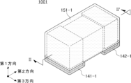
FIG. 6 is a schematic perspective view of a multilayer
図6及び図7を参照すると、本発明の一実施形態による積層型電子部品1001は、第1めっき層141-1及び第2めっき層142-1が第1面の延長線以下に配置されることができる。これにより、実装時にはんだの高さを最小化することができ、実装空間を最小化することができる。
Referring to FIGS. 6 and 7, in a multilayer
また、絶縁層151-1は、第1面の延長線以下まで延びて第1めっき層141-1及び第2めっき層142-1と接するように配置されることができる。 Also, the insulating layer 151-1 may be arranged to extend below the extension line of the first surface and contact the first plating layer 141-1 and the second plating layer 142-1.
図8は、本発明の一実施形態による積層型電子部品1002を概略的に示した斜視図であり、図9は、図8のIII-III'線に沿った断面図である。
FIG. 8 is a schematic perspective view of a multilayer
図8及び図9を参照すると、本発明の一実施形態による積層型電子部品1002は、第1面1上に配置され、第1バンド部131bと第2バンド部132bとの間に配置される追加絶縁層161をさらに含むことができる。これにより、高圧電流下で第1バンド部131bと第2バンド部132bとの間で発生し得る漏れ電流などを防止することができる。
8 and 9, a multilayer
追加絶縁層161の種類は特に限定する必要はない。例えば、追加絶縁層161は、絶縁層151と同様に、Tiを含む酸化物を含むことができ、TiO2を含むことができ、TiO2であることができる。但し、追加絶縁層161及び絶縁層151を同一材料に限定する必要はなく、相違する材料から形成することもできる。例えば、エポキシ樹脂、アクリル樹脂、エチルセルロース(Ethyl Cellulose)などから選択された1種以上を含むか、ガラスを含むことができる。
The type of additional insulating
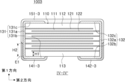
図10は、本発明の一実施形態による積層型電子部品1003を概略的に示した斜視図であり、図11は、図10のIV-IV'線に沿った断面図である。
FIG. 10 is a schematic perspective view of a multilayer
図10及び図11を参照すると、一実施形態による積層型電子部品1003は、第1面1から上記第1内部電極121及び第2内部電極122のうち、上記第1面1に最も近く配置された内部電極までの第1方向の平均サイズをH1とし、上記第1面1の延長線から上記第1接続部131a及び第2接続部132a上に配置されためっき層141-3、142-3の端までの第1方向の平均サイズをH2とするとき、H1<H2を満たすことができる。これによって、実装時にはんだと接する面積を増加させて固着強度を向上させることができる。
Referring to FIGS. 10 and 11, the multilayer
より好ましくは、本体110の第1方向の平均サイズをTとするとき、H2<T/2を満たすことができる。すなわち、H1<H2<T/2を満たすことができる。H2がT/2以上の場合には、絶縁層による耐湿信頼性向上の効果が低下するおそれがあるためである。
More preferably, H2<T/2, where T is the average size of the
H1、H2及びTは、本体110を第3方向に等間隔を有する5つの地点で第1方向及び第2方向に切断した断面(L-T断面)で測定した値を平均した値であることができる。H1は各断面において、第1面1に最も近く配置された内部電極が外部電極と連結される地点で測定した値を平均した値であることができ、H2は各断面において、外部電極と接するめっき層の端を基準に測定した値を平均した値であることができ、H1及びH2の測定時に基準となる第1面の延長線は同一であることができる。また、Tは、各断面において、本体110の第1方向の最大サイズを測定した後の平均値であることができる。
H1, H2 and T are average values of values measured in cross sections (LT cross sections) obtained by cutting the
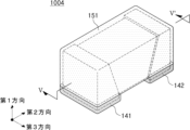
図12は、本発明の一実施形態による積層型電子部品1004を概略的に示した斜視図であり、図13は、図12のV-V'線に沿った断面図である。
FIG. 12 is a schematic perspective view of a multilayer
図12及び図13を参照すると、本発明の一実施形態による積層型電子部品1004は、第1バンド部131b-4の平均長さB1が第3バンド部131c-4の平均長さB3より長いことができ、第2バンド部132b-4の平均長さが第4バンド部132c-4の平均長さB4よりも長いことができる。これによって、実装時にはんだと接する面積を増加させて固着強度を向上させることができる。
12 and 13, in the multilayer
より詳細には、第3面3の延長線から上記第1バンド部131b-4の端までの上記第2方向の平均サイズをB1とし、上記第4面4の延長線から上記第2バンド部132b-4の端までの上記第2方向の平均サイズをB2とし、上記第3面3の延長線から上記第3バンド部131c-4の端までの上記第2方向の平均サイズをB3とし、上記第4面4の延長線から上記第4バンド部132c-4の端までの上記第2方向の平均サイズをB4とするとき、B3<B1及びB4<B2を満たすことができる。
More specifically, the average size in the second direction from the extension line of the
このとき、本体110の第2方向の平均サイズをLとするとき、0.2≦B1/L≦0.4及び0.2≦B2/L≦0.4を満たすことができる。
At this time, 0.2≦B1/L≦0.4 and 0.2≦B2/L≦0.4 may be satisfied, where L is the average size of the
B1、B2、B3、B4及びLは、本体110を第3方向に等間隔を有する5つの地点で第1方向及び第2方向に切断した断面(L-T断面)で測定した値を平均した値であることができる。
B1, B2, B3, B4, and L are average values measured in cross sections (LT cross sections) obtained by cutting the
また、第1外部電極131-4は、第1接続部131a-4から第5面及び第6面の一部まで延びる第1側面バンド部を含むことができ、第2外部電極132-4は、第2接続部132a-4から第5面及び第6面の一部まで延びる第2側面バンド部を含むことができる。このとき、上記第1側面バンド部及び第2側面バンド部の第2方向のサイズは、第1面に近づくほど徐々に大きくなることができる。すなわち、上記第1側面バンド部及び第2側面バンド部は、テーパ状や台形状に配置されることができる。
In addition, the first external electrode 131-4 may include a first side band portion extending from the
さらに、上記第3面の延長線から上記第3バンド部141c-4の端までの上記第2方向の平均サイズをB3とし、上記第4面の延長線から上記第4バンド部142c-4の端までの上記第2方向の平均サイズをB4とし、上記第3面と上記第2内部電極122とが離隔した領域の第2方向の平均サイズをG1とし、上記第4面と上記第1内部電極121とが離隔した領域の第2方向の平均サイズをG2とするとき、B3≦G1及びB4≦G2を満たすことができる。これにより、外部電極が占める体積を最小化して積層型電子部品1004の単位体積当たりの容量を増加させることができる。
Further, the average size in the second direction from the extension line of the third surface to the end of the third band portion 141c-4 is B3, and the length of the fourth band portion 142c-4 from the extension line of the fourth surface is defined as B3. Let B4 be the average size in the second direction up to the end, let G1 be the average size in the second direction of the region where the third surface and the second
上記G1及びG2は、本体を第3方向の中央から第1方向及び第2方向に切断した断面において、第1方向の中央部に位置した任意の5つの第2内部電極に対して測定した第3面まで離隔した第2方向のサイズを平均した値はG1とし、第1方向の中央部に位置した任意の5つの第1内部電極に対して測定した第4面まで離隔した領域の第2方向のサイズを平均した値をG2とすることができる。 G1 and G2 above are measured for arbitrary five second internal electrodes positioned at the center in the first direction in a cross section obtained by cutting the main body in the first direction and the second direction from the center in the third direction. The value obtained by averaging the sizes in the second direction separated by three surfaces is G1, and the size of the area separated by the fourth surface measured for arbitrary five first internal electrodes positioned in the central portion in the first direction is the second dimension of the area separated by the fourth surface. G2 can be the averaged size of the directions.
さらに、本体110を第3方向に等間隔を有する5つの地点で第1方向及び第2方向に切断した断面(L-T断面)でG1及びG2を求め、それらを平均した値をG1及びG2として、さらに一般化することができる。
Furthermore, G1 and G2 are obtained in cross sections (LT cross sections) obtained by cutting the
但し、本発明をB3≦G1及びB4≦G2に限定する意図ではなく、B3≧G1及びB4≧G2を満たす場合も本発明の一実施形態に含まれることができる。したがって、一実施形態において、第3面の延長線から第3バンド部の端までの上記第2方向の平均サイズをB3とし、上記第4面の延長線から上記第4バンド部の端までの上記第2方向の平均サイズをB4とし、第3面と上記第2内部電極とが離隔した領域の第2方向の平均サイズをG1とし、第4面と上記第1内部電極とが離隔した領域の第2方向の平均サイズをG2とするとき、B3≧G1及びB4≧G2を満たすことができる。 However, the present invention is not intended to be limited to B3≦G1 and B4≦G2, and cases where B3≧G1 and B4≧G2 are satisfied may also be included in an embodiment of the present invention. Therefore, in one embodiment, the average size in the second direction from the extension of the third surface to the end of the third band portion is B3, and the average size from the extension of the fourth surface to the end of the fourth band portion is B3. Let B4 be the average size in the second direction, G1 be the average size in the second direction of the region where the third surface and the second internal electrode are separated, and G1 be the region where the fourth surface and the first internal electrode are separated. B3≧G1 and B4≧G2, where G2 is the average size in the second direction of .
一実施形態において、上記第3面E3の延長線から上記第1バンド部の端までの上記第2方向の平均サイズをB1とし、上記第4面の延長線から上記第2バンド部の端までの上記第2方向の平均サイズをB2とするとき、B1≧G1及びB2≧G2を満たすことができる。これにより、積層型電子部品1004の基板180との固着強度を向上させることができる。
In one embodiment, B1 is the average size in the second direction from the extension of the third surface E3 to the end of the first band portion, and the extension of the fourth surface to the end of the second band portion. B1≧G1 and B2≧G2, where B2 is the average size in the second direction. Thereby, the bonding strength of the laminated
図14は、本発明の一実施形態による積層型電子部品1005を概略的に示した斜視図であり、図15は、図14のVI-VI'線に沿った断面図である。
FIG. 14 is a schematic perspective view of a multilayer
図14及び図15を参照すると、本発明の一実施形態による積層型電子部品1005の第1外部電極131-5及び第2外部電極132-5は、第2面上には配置されず、第3面、第4面及び第1面に配置されてL字状を有することができる。すなわち、第1外部電極131-5及び第2外部電極132-5は、第2面の延長線以下に配置されることができる。
14 and 15, the first external electrode 131-5 and the second external electrode 132-5 of the multilayer
第1外部電極131-5は、第3面3に配置される第1接続部131a-5、上記第1接続部131a-5から上記第1面1の一部まで延びる第1バンド部131b-5を含むことができ、第2外部電極132-5は、第4面4に配置される第2接続部132a-5、上記第2接続部132a-5から上記第1面1の一部まで延びる第2バンド部132b-5を含むことができる。第2面2上には外部電極131-5、132-5が配置されず、絶縁層151-5が第2面2の全部を覆うように配置されることができる。これにより、外部電極131-5、132-5が占める体積を最小化することができるので、積層電子部品1005の単位体積当たりの容量をより向上させることができる。但し、絶縁層151-5が第2面2の全部を覆う形態で限定する必要はなく、絶縁層が第2面2の一部または全部を覆わずに分離されて第1接続部131a-5及び第2接続部132a-5をそれぞれ覆っている形態を有することもできる。
The first external electrode 131-5 includes a first connecting
第1バンド部131b-5上には第1めっき層141-5、第2バンド部132b-5上には第2めっき層142-5が配置され、第1めっき層141-5及び第2めっき層142-5は、第1接続部132a-5及び第2接続部132b-5上の一部まで延びて配置されることができる。
A first plating layer 141-5 is arranged on the
このとき、第5面5及び第6面6上にも外部電極131-5、132-5が配置されないことができる。すなわち、外部電極131-5、132-5が第3面、第4面及び第1面上にのみ配置される形態を有することができる。
At this time, the external electrodes 131-5 and 132-5 may not be arranged on the
第1面1から上記第1内部電極121及び第2内部電極122のうち、上記第1面1に最も近く配置された内部電極までの第1方向の平均サイズをH1とし、上記第1面1の延長線から上記第1接続部131a-5及び第2接続部132a-5上に配置されためっき層141-5、142-5の端までの第1方向の平均サイズをH2とするとき、H1<H2を満たすことができる。これによって、実装時にはんだと接する面積を増加させて固着強度を向上させることができ、外部電極131-5、132-5とめっき層141-5、142-5とが接する面積を増加させてESR(Equivalent Series Resistance)が増加されることを抑制することができる。
Let H1 be the average size in the first direction from the
より好ましくは、本体110の第1方向の平均サイズをTとするとき、H2<T/2を満たすことができる。すなわち、H1<H2<T/2を満たすことができる。H2がT/2以上である場合には、絶縁層による耐湿信頼性向上の効果が低下するおそれがあるためである。
More preferably, H2<T/2, where T is the average size of the
また、第1めっき層141-5及び第2めっき層142-5は、第3面及び第4面において、絶縁層151-1の一部を覆うように配置されることができる。すなわち、めっき層141-5、142-5が第3面及び第4面で絶縁層151-5の端を覆うように配置されることができる。これにより、絶縁層151-5とめっき層141-5、142-5との結合力を強化して積層型電子部品1005の信頼性を向上させることができる。
Also, the first plating layer 141-5 and the second plating layer 142-5 may be arranged to partially cover the insulating layer 151-1 on the third and fourth surfaces. That is, the plating layers 141-5 and 142-5 may be arranged to cover the edges of the insulating layer 151-5 on the third and fourth surfaces. As a result, the bonding strength between the insulating layer 151-5 and the plating layers 141-5 and 142-5 can be strengthened, and the reliability of the multilayer
また、絶縁層151-5は、第3面及び第4面で第1めっき層141-5及び第2めっき層142-5の一部を覆うように配置されることができる。すなわち、絶縁層151-5が第3面及び第4面でめっき層141-5、142-5の端を覆うように配置されることができる。これにより、絶縁層151-5とめっき層141-5、142-5との結合力を強化して積層型電子部品1005の信頼性を向上させることができる。
Also, the insulating layer 151-5 may be arranged to partially cover the first plating layer 141-5 and the second plating layer 142-5 on the third and fourth surfaces. That is, the insulating layer 151-5 may be arranged to cover the edges of the plating layers 141-5 and 142-5 on the third and fourth surfaces. As a result, the bonding strength between the insulating layer 151-5 and the plating layers 141-5 and 142-5 can be strengthened, and the reliability of the multilayer
図16は、図14の変形例を示したものである。図16を参照すると、本発明の一実施形態による積層型電子部品1005の変形例1006は、第1接続部131a-6と第3面との間には、第1追加電極層134が配置されることができ、第2接続部132a-6と第4面との間には、第2追加電極層135が配置されることができる。第1追加電極層134は、第3面から逸脱しない範囲で配置されることができ、第2追加電極層135は、第4面から逸脱しない範囲で配置されることができる。第1追加電極層134及び第2追加電極層135は、内部電極121、122と外部電極131-6、132-6との間の電気的連結性を向上させることができ、外部電極131-6、132-6との結合力に優れて、外部電極131-6、132-6の機械的結合力をより向上させる役割を果たすことができる。
FIG. 16 shows a modified example of FIG. Referring to FIG. 16, a modified example 1006 of the multilayer
第1外部電極131-6及び第2外部電極132-6は、第2面上に第1外部電極及び第2外部電極が配置されないL字状を有することができる。 The first external electrode 131-6 and the second external electrode 132-6 may have an L shape in which the first external electrode and the second external electrode are not arranged on the second surface.
第1外部電極131-6は、第1追加電極層134上に配置される第1接続部131a-6、及び上記第1接続部131a-6から上記第1面1の一部まで延びる第1バンド部131b-6を含むことができ、第2外部電極132-6は、第2追加電極層135上に配置される第2接続部132a-6、及び上記第2接続部132a-6から上記第1面1の一部まで延びる第2バンド部132b-6を含むことができる。
The first external electrode 131-6 includes a first connecting
一方、第1追加電極層131-6及び第2追加電極層132-6は、金属などのように電気導電性を有するものであれば、如何なる物質を用いても形成することができ、電気的特性、構造的安定性などを考慮して具体的な物質が決定されることができる。また、第1追加電極層131-6及び第2追加電極層132-6は、導電性金属及びガラスを含む焼成(firing)電極であるか、または導電性金属及び樹脂を含む樹脂系電極であることができる。また、第1追加電極層131-6及び第2追加電極層132-6は、本体上に導電性金属を含むシートを転写する方式で形成されたものであることができる。 On the other hand, the first additional electrode layer 131-6 and the second additional electrode layer 132-6 can be formed using any material having electrical conductivity such as metal. Specific materials can be determined in consideration of properties, structural stability, and the like. Also, the first additional electrode layer 131-6 and the second additional electrode layer 132-6 are firing electrodes containing conductive metal and glass, or resin-based electrodes containing conductive metal and resin. be able to. Also, the first additional electrode layer 131-6 and the second additional electrode layer 132-6 may be formed by transferring a sheet containing a conductive metal onto the body.
第1追加電極層131-6及び第2追加電極層132-6に含まれる導電性金属として電気導電性に優れた材料を用いることができ、特に限定しない。例えば、導電性金属は、Cu、Ni、Pd、Ag、Sn、Cr及びそれらの合金のうち1つ以上であることができる。好ましくは、第1追加電極層131-6及び第2追加電極層132-6は、Ni及びNi合金のうち1つ以上を含むことができ、これによって、Niを含む内部電極121、122との連結性をより向上させることができる。
As the conductive metal contained in the first additional electrode layer 131-6 and the second additional electrode layer 132-6, a material with excellent electrical conductivity can be used, and the material is not particularly limited. For example, the conductive metal can be one or more of Cu, Ni, Pd, Ag, Sn, Cr and alloys thereof. Preferably, the first additional electrode layer 131-6 and the second additional electrode layer 132-6 may contain one or more of Ni and Ni alloys, so that the
図17は、本発明の一実施形態による積層型電子部品1007を概略的に示した斜視図であり、図18は、図17のVII-VII'線に沿った断面図である。
FIG. 17 is a schematic perspective view of a multilayer
図17及び図18を参照すると、本発明の一実施形態による積層型電子部品1007の第1めっき層141-6及び第2めっき層142-6の平均厚さt1は絶縁層151-6の平均厚さt2よりも薄い形態であることができる。
17 and 18, the average thickness t1 of the first plating layer 141-6 and the second plating layer 142-6 of the multilayer
絶縁層151-6は、外部からの水分またはめっき液の浸透を防止する役割を果たすが、めっき層141-6、142-6との連結性が弱くてめっき層141-6、142-6のデラミネーション(delamination)の原因となることがある。めっき層がデラミネーションされる場合、基板180との固着強度が低下することがある。ここで、めっき層141-6、142-6のデラミネーションとは、めっき層が一部剥離するか、または外部電極131-5、132-5と物理的に分離されることを意味することができる。めっき層と絶縁層との連結性が弱いので、絶縁層とめっき層との界面の隙間が広がったり、異物が浸透する可能性が高くなったり、外部衝撃などに脆くなってデラミネーションされる可能性が高くなったりすることがある。
The insulating layer 151-6 serves to prevent moisture or plating solution from permeating from the outside. It may cause delamination. When the plating layer is delaminated, the bonding strength with the
本発明の一実施形態によると、めっき層の平均厚さt1を絶縁層の平均厚さt2よりも薄くしてめっき層と絶縁層が当接する面積を減らすことができ、これによって、デラミネーションの発生を抑制して、積層型電子部品1000の基板180との固着強度を向上させることができる。
According to one embodiment of the present invention, the average thickness t1 of the plating layer can be less than the average thickness t2 of the insulating layer to reduce the contact area between the plating layer and the insulating layer, thereby improving the delamination. It is possible to suppress the occurrence and improve the bonding strength between the multilayer
第1めっき層141-6及び第2めっき層142-6の平均厚さt1は、第1接続部131a-5及び第2接続部132a-5または第1バンド部131b-5及び第2バンド部132b-5上の等間隔の5つの地点で測定した厚さを平均した値であることができ、絶縁層151-6の平均厚さt2は第1接続部131a-5及び第2接続部132a-5上の等間隔の5つの地点で測定した厚さを平均した値であることができる。
The average thickness t1 of the first plating layer 141-6 and the second plating layer 142-6 is the
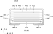
図19は、本発明の一実施形態による積層型電子部品2000を概略的に示した斜視図であり、図20は、図19のVIII-VIII'線に沿った断面図である。
FIG. 19 is a schematic perspective view of a multilayer
以下、図19及び図20を参照して、本発明の一実施形態による積層型電子部品2000について詳細に説明する。但し、上述した内容と重複する内容は、重複した説明を避けるために省略することができる。
Hereinafter, a multilayer
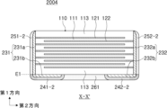
本発明の一実施形態による積層型電子部品2000は、誘電体層111、上記誘電体層を間に挟んで交互に配置される第1内部電極121及び第2内部電極122を含み、第1方向に対向する第1面1及び第2面2、上記第1面及び第2面と連結され、第2方向に対向する第3面3及び第4面4、並びに上記第1面~第4面と連結され、第3方向に対向する第5面5及び第6面6を含む本体110と、上記第3面に配置される第1連結電極231a及び上記第1面に配置されて上記第1連結電極と連結される第1バンド電極231bを含む第1外部電極231と、上記第4面に配置される第2連結電極232a及び上記第1面に配置されて上記第2連結電極と連結される第2バンド電極232bを含む第2外部電極232と、上記第1連結電極上に配置される第1絶縁層251と、上記第2連結電極上に配置される第2絶縁層252と、上記第1バンド電極上に配置される第1めっき層241と、上記第2バンド電極上に配置される第2めっき層242と、を含み、上記第1絶縁層251及び第2絶縁層252はTiを含む酸化物を含み、上記誘電体層は、BaTiO3、(Ba1-xCax)TiO3(0<x<1)、Ba(Ti1-yCay)O3(0<y<1)、(Ba1-xCax)(Ti1-yZry)O3(0<x<1、0<y<1)及びBa(Ti1-yZry)O3(0<y<1)のうち1つを主成分として含むことができる。
A multilayer
第1連結電極231aは、第3面3に配置されて第1内部電極121と連結され、第2連結電極231bは、第4面4に配置されて第2内部電極121と連結されることができる。また、第1連結電極231a'上には第1絶縁層251が配置され、第2連結電極232a上には第2絶縁層252が配置されることができる。
The
従来には、外部電極を形成する際に導電性金属が含まれたペーストを用いて、本体の内部電極が露出した面をペーストにディッピング(dipping)する方法が主に用いられた。しかしながら、ディッピング(dipping)工法によって形成された外部電極は、厚さ方向の中央部における外部電極の厚さが厚すぎる可能性があった。また、このようなディッピング(dipping)工法による外部電極の厚さ不均衡の問題ではなくても、本体の第3面及び第4面に内部電極が露出するので、外部電極を介する水分及びめっき液の浸透を抑制するために、第3面及び第4面に配置された外部電極の厚さが一定以上になるように形成した。 Conventionally, when the external electrodes are formed, a paste containing a conductive metal is used, and a method of dipping the exposed surface of the internal electrodes of the main body into the paste has been mainly used. However, the external electrodes formed by the dipping method may be too thick at the central portion in the thickness direction. In addition, even if the dipping method is not a problem of thickness imbalance of the external electrodes, the internal electrodes are exposed on the third and fourth surfaces of the main body, so that moisture and plating solution can pass through the external electrodes. In order to suppress the permeation of , the thickness of the external electrodes arranged on the third and fourth surfaces is set to a certain value or more.
一方、本発明では、連結電極231a、232a上に絶縁層251、252を配置するので、内部電極が露出する第3面及び第4面における連結電極231a、232aの厚さを薄くしても十分な信頼性を確保することができる。
On the other hand, in the present invention, since the insulating
第1連結電極231a及び第2連結電極232aは、それぞれ第3面及び第4面に対応する形態であることができ、第1連結電極231a及び第2連結電極232aにおいて本体110に向かう面は、本体110の第3面及び第4面とそれぞれ同一面積を有することができる。第1連結電極231a及び第2連結電極232aは、それぞれ第3面3及び第4面4から逸脱しない範囲で配置されることができる。連結電極231a、232aは、本体110の第1面1、第2面2、第5面5、及び第6面6に延びないように配置されることができる。具体的には、一実施形態において、第1連結電極231a及び第2連結電極232aは第5面及び第6面と離隔して配置されることができる。これにより、内部電極121、122と外部電極231、232との間の十分な連結性を確保しながらも、外部電極が占める体積を最小化して、積層型電子部品2000の単位体積当たりの容量を増加させることができる。
The
この観点から、上記第1連結電極231a及び第2連結電極232aは、上記第2面2と離隔して配置されることができる。すなわち、外部電極231、232が第2面上には配置されないので、外部電極231、232が占める体積をさらに最小化し、積層型電子部品2000の単位体積当たりの容量をさらに増加させることができる。
From this point of view, the
但し、連結電極231a、232aは、本体110のコーナーに延びてコーナー上に配置されたコーナー部を含むことができる。すなわち、一実施形態において、第1連結電極は、上記第1-3コーナー及び第2-3コーナー上に延びて配置されるコーナー部を含み、上記第2連結電極は、上記第1-4コーナー及び第2-4コーナー上に延びて配置されるコーナー部を含むことができる。
However, the
さらに、連結電極231a、232aは、従来のディッピング方式によって形成された外部電極に対して均一かつ薄い厚さを有することができる。
In addition, the
連結電極231a、232aを形成する方法は特に制限する必要はないが、例えば、導電性金属、バインダーなどの有機物質などを含むシートを第3面及び第4面に転写する方式で形成することができる。
The method of forming the
連結電極231a、232aの厚さは特に限定しないが、例えば、2~7μmであることができる。ここで、連結電極231a、232aの厚さとは、最大厚さを意味することができ、連結電極231a、232aの第2方向のサイズを意味することができる。
Although the thickness of the connecting
一実施形態において、第1連結電極231a及び第2連結電極232aは、内部電極121、122に含まれた金属と同一の金属及びガラスを含むことができる。第1連結電極231a及び第2連結電極232aが内部電極121、122に含まれた金属と同一の金属を含むことにより、内部電極121、122との電気的連結性を向上させることができ、第1連結電極231a及び第2連結電極232aがガラスを含むことによって、本体110及び/または絶縁層251、252との結合力を向上させることができる。このとき、内部電極121、122に含まれた金属と同一の金属はNiであることができる。
In one embodiment, the
第1絶縁層251及び第2絶縁層252は、それぞれ第1連結電極231a及び第2連結電極232a上に配置され、第1連結電極231a及び第2連結電極232a上にめっき層が形成されることを防止する役割を果たすことができる。また、第1絶縁層251及び第2絶縁層252は、シーリング特性を向上させ、外部から水分やめっき液などが浸透することを最小化する役割を果たすことができる。
The first insulating
第1絶縁層251及び第2絶縁層252は、Tiを含む酸化物を含むことができる。第1絶縁層251及び第2絶縁層252にガラス系列の代わりにTiを含む酸化物を適用することで、耐湿信頼性をより向上させることができ、熱収縮によるクラック、金属拡散による放射クラックなどを抑制することができる。
The first insulating
第1バンド電極231b及び第2バンド電極232bは、本体110の第1面1に配置されることができる。第1バンド電極231b及び第2バンド電極232bは、それぞれ第1連結電極231a及び第2連結電極232aと接触することによって、第1内部電極121及び第2内部電極122とそれぞれ電気的に連結されることができる。
The
従来のディッピング(dipping)工法によって形成された外部電極は、第3面及び第4面で厚く形成され、第1面、第2面、第5面及び第6面にも一部延びて形成されることによって、有効体積率を高く確保することが困難であるという問題点があった。 The external electrodes formed by the conventional dipping method are thickly formed on the third and fourth surfaces and partially extended on the first, second, fifth and sixth surfaces. Therefore, there is a problem that it is difficult to secure a high effective volume ratio.
一方、本発明の一実施形態によると、内部電極が露出した面には第1連結電極231a及び第2連結電極232aを配置し、基板に実装される面には、第1バンド電極231b及び第2バンド電極232bを配置することによって、有効体積率を高く確保することができる。
Meanwhile, according to an embodiment of the present invention, the
一方、内部電極121、122が第1方向に積層されている場合には、内部電極121、122が実装面と平行になるように、積層型電子部品2000を基板に水平実装することができる。但し、本発明が水平実装である場合に限定されるものではなく、内部電極121、122を第3方向に積層する場合には、内部電極121、122が実装面と垂直になるように、基板に積層型電子部品を垂直実装することができる。
On the other hand, when the
第1バンド電極231b及び第2バンド電極232bは、金属などのように電気導電性を有するものであれば、如何なる物質を用いても形成することができ、電気的特性、構造的安定性などを考慮して具体的な物質が決定されることができる。例えば、第1バンド電極231b及び第2バンド電極232bは、導電性金属及びガラスを含む焼成(firing)電極であることができ、本体の第1面に導電性金属及びガラスを含むペーストを塗布する方式を用いて形成することができるが、これに制限されるものではなく、導電性金属を本体の第1面にめっきしためっき層であることができる。
The
第1バンド電極231b及び第2バンド電極232bに含まれる導電性金属として電気導電性に優れた材料を用いることができ、特に限定されない。例えば、導電性金属は、ニッケル(Ni)、銅(Cu)、及びそれらの合金のうち1つ以上であることができ、内部電極121、122に含まれた金属と同一の金属を含むことができる。
A material having excellent electrical conductivity can be used as the conductive metal contained in the
一方、一実施形態において、第1外部電極231は、上記第2面2に配置されて上記第1連結電極231aと連結される第3バンド電極(図示せず)をさらに含み、上記第2外部電極232は、上記第2面2に配置されて上記第2連結電極232aと連結される第4バンド電極(図示せず)をさらに含むことができる。
Meanwhile, in one embodiment, the first
一実施形態において、上記第3面の延長線E3から上記第1バンド電極231bの端までの距離をB1とし、上記第4面の延長線E4から上記第2バンド電極232bの端までの距離をB2とし、上記第3面の延長線から上記第3バンド電極(図示せず)の端までの距離をB3とし、上記第4面の延長線から上記第4バンド電極(図示せず)の端までの距離をB4とし、上記第3面と上記第2内部電極122とが離隔した領域の第2方向の平均サイズをG1とし、上記第4面と上記第1内部電極121とが離隔した領域の第2方向の平均サイズをG2とするとき、B1≧G1、B3≦G1、B2≧G2及びB4≦G2を満たすことができる。これにより、外部電極が占める体積を最小化して、積層型電子部品2000の単位体積当たりの容量を増加させるとともに、実装時にはんだと接する面積を増加させて固着強度を向上させることができる。
In one embodiment, the distance from the extension line E3 of the third surface to the end of the
但し、本発明をB1≧G1、B3≦G1、B2≧G2及びB4≦G2に限定する意図ではなく、B1≧G1、B3≧G1、B2≧G2及びB4≧G2を満たす場合も本発明の一実施形態に含まれることができる。したがって、一実施形態において、上記第3面の延長線E3から上記第1バンド電極231bの端までの距離をB1とし、上記第4面の延長線E4から上記第2バンド電極232bの端までの距離をB2とし、上記第3面の延長線から上記第3バンド電極(図示せず)の端までの距離をB3とし、上記第4面の延長線から上記第4バンド電極(図示せず)の端までの距離をB4とし、上記第3面と上記第2内部電極122とが離隔した領域の第2方向の平均サイズをG1とし、上記第4面と上記第1内部電極121とが離隔した領域の第2方向の平均サイズをG2とするとき、B1≧G1、B3≧G1、B2≧G2及びB4≧G2を満たすことができる。これにより、第1面及び第2面のいずれか一面を実装面とすることができ、実装便宜性を向上させることができる。
However, the present invention is not intended to be limited to B1≧G1, B3≦G1, B2≧G2 and B4≦G2. can be included in an embodiment. Therefore, in one embodiment, the distance from the extension line E3 of the third surface to the end of the
第1めっき層241及び第2めっき層242は、第1バンド電極231b及び第2バンド電極232b上に配置されることができる。第1めっき層241及び第2めっき層242は実装特性を向上させる役割を果たす。第1めっき層241及び第2めっき層242の種類は特に限定されず、Ni、Sn、Pd及びこれらの合金のうち1つ以上を含むめっき層であることができ、複数層で形成されることができる。
A
第1めっき層241及び第2めっき層242に対するより具体的な例を挙げると、第1めっき層241及び第2めっき層242は、Niめっき層またはSnめっき層であることができ、第1バンド電極231b及び第2バンド電極232b上にNiめっき層及びSnめっき層が順次形成された形態であることができる。
As a more specific example of the
一実施形態において、第1めっき層241及び第2めっき層242は、それぞれ第1連結電極231a及び第2連結電極232aを一部覆うように延びて配置されることができる。
In one embodiment, the
第1面1から第1内部電極121及び第2内部電極122のうち、第1面1に最も近く配置された内部電極までの第1方向の平均サイズをH1とし、上記第1面1の延長線から上記第1連結電極231a及び第2連結電極232a上に配置された第1めっき層241及び第2めっき層242の端までの第1方向の平均サイズをH2とするとき、H1>H2(又はH1≧H2)を満たすことができる。これにより、めっき工程時にめっき液が内部電極に浸透することを抑制して信頼性を向上させることができる。
Let H1 be the average size in the first direction from the
一実施形態において、第1絶縁層251及び第2絶縁層252は、第1連結電極231a及び第2連結電極232aとそれぞれ直接接するように配置され、第1連結電極231a及び第2連結電極232aは、導電性金属及びガラスを含むことができる。これにより、第1連結電極231a及び第2連結電極232aの外表面のうち絶縁層251、252が配置された領域には、めっき層241、242が配置されないことがあるので、めっき液による外部電極の侵食を効果的に防止することができる。
In one embodiment, the
一実施形態において、第1めっき層241は、第1絶縁層251の第1外部電極231上に配置された端を覆うように配置され、第2めっき層242は、第2絶縁層252の第2外部電極232上に配置された端を覆うように配置されることができる。これにより、絶縁層251、252とめっき層241、242との結合力を強化して積層型電子部品2000の信頼性を向上させることができる。また、外部電極231、232上にめっき層241、242を形成する前に第1絶縁層251及び第2絶縁層252を先に形成することで、めっき層の形成過程におけるめっき液の浸透をより確実に抑制することができる。めっき層よりも絶縁層を先に形成することによって、めっき層241、242が絶縁層251、252の端を覆う形態を有することができる。
In one embodiment, the
一実施形態において、第1絶縁層251は、第1めっき層241の第1外部電極231上に配置された端を覆うように配置され、第2絶縁層252は、第2めっき層242の第2外部電極232上に配置された端を覆うように配置されることができる。これにより、絶縁層251とめっき層241、242との結合力を強化して積層型電子部品2000の信頼性を向上させることができる。
In one embodiment, the first insulating
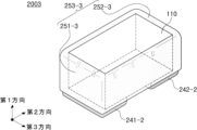
図21は、図19の変形例を示したものである。図21を参照すると、本発明の一実施形態による積層型電子部品2000の変形例2001は、第1絶縁層251-1及び第2絶縁層252-1が第5面5及び第6面6に延びて互いに連結されることで、1つの絶縁層253-1に連結されることができる。このとき、第1絶縁層及び第2絶縁層が連結された絶縁層253-1が第5面及び第6面の一部を覆うように配置されることができる。
FIG. 21 shows a modification of FIG. Referring to FIG. 21, a modified example 2001 of a multilayer
図22は、本発明の一実施形態による積層型電子部品2002を概略的に示した斜視図であり、図23は、図22のIX-IX'線に沿った断面図である。
FIG. 22 is a schematic perspective view of a multilayer
図22及び図23を参照すると、本発明の一実施形態による積層型電子部品2002は、第1めっき層241-2及び第2めっき層242-2が第1面の延長線以下に配置されることができる。これにより、実装時にはんだの高さを最小化することができ、実装空間を最小化することができる。
Referring to FIGS. 22 and 23, in a multilayer
また、第1絶縁層251-2及び第2絶縁層252-2は、第1面の延長線以下まで延びて第1めっき層241-2及び第2めっき層242-2と接するように配置されることができる。 In addition, the first insulating layer 251-2 and the second insulating layer 252-2 are arranged so as to extend below the extension line of the first surface and contact the first plating layer 241-2 and the second plating layer 242-2. can
図24は、図22の変形例を示したものである。図24を参照すると、本発明の一実施形態による積層型電子部品2002の変形例2003は、第1絶縁層251-3及び第2絶縁層252-3が第5面5及び第6面6に延びて互いに連結されることで、1つの絶縁層253-3に連結されることができる。このとき、第1絶縁層及び第2絶縁層が連結された絶縁層253-3が第5面及び第6面の全部を覆うように配置されることができる。
FIG. 24 shows a modification of FIG. Referring to FIG. 24, a modified example 2003 of a multilayer
図25は、本発明の一実施形態による積層型電子部品2004を概略的に示した斜視図であり、図26は、図25のX-X'線に沿った断面図である。
FIG. 25 is a schematic perspective view of a multilayer
図25及び図26を参照すると、本発明の一実施形態による積層型電子部品2004は、第1面1上に配置され、第1バンド電極231bと第2バンド電極232bとの間に配置される追加絶縁層261をさらに含むことができる。これにより、高圧電流下で第1バンド電極231bと第2バンド電極232bとの間で発生し得る漏れ電流などを防止することができる。
25 and 26, the multilayer
追加絶縁層261の種類は特に限定する必要はない。例えば、追加絶縁層261は、第1絶縁層251-2及び第2絶縁層252-2と同様に、Tiを含む酸化物を含むことができ、TiO2を含むことができ、TiO2であることができる。但し、追加絶縁層261と第1絶縁層251-2及び第2絶縁層252-2を同一材料に限定する必要はなく、相違する材料から形成されることもできる。例えば、エポキシ樹脂、アクリル樹脂、エチルセルロース(Ethyl Cellulose)などから選択された1種以上を含むか、またはガラスを含むことができる。
The type of additional insulating
図27は、図25の変形例を示したものである。図27を参照すると、本発明の一実施形態による積層型電子部品2004の変形例2005は、第1絶縁層251-5及び第2絶縁層252-5が第5面5及び第6面6に延びて互いに連結されることで、1つの絶縁層253-5に連結されることができる。
FIG. 27 shows a modification of FIG. Referring to FIG. 27, a modified example 2005 of a multilayer
図28は、本発明の一実施形態による積層型電子部品2006を概略的に示した斜視図であり、図29は、図28のXI-XI'線に沿った断面図である。
FIG. 28 is a schematic perspective view of a multilayer
図28及び図29を参照すると、一実施形態による積層型電子部品2006は、第1連結電極231a上に配置される第1絶縁層251-6、及び第2連結電極232a上に配置される第2絶縁層252-6を含み、第1面1から上記第1内部電極121及び第2内部電極122のうち、上記第1面1に最も近く配置された内部電極までの第1方向の平均サイズをH1とし、上記第1面1の延長線から上記第1連結電極231a及び第2連結電極232a上に配置されためっき層241-6、242-6の端までの第1方向の平均サイズをH2とするとき、H1<H2を満たすことができる。これによって、実装時にはんだと接する面積を増加させて固着強度を向上させることができる。
28 and 29, the multilayer
より好ましくは、本体110の第1方向の平均サイズをTとするとき、H2<T/2を満たすことができる。すなわち、H1<H2<T/2を満たすことができる。H2がT/2以上である場合には、絶縁層による耐湿信頼性向上の効果が低下するおそれがあるためである。
More preferably, H2<T/2, where T is the average size of the
図30は、図28の変形例を示したものである。図30を参照すると、本発明の一実施形態による積層型電子部品2006の変形例2007は、第1絶縁層251-7及び第2絶縁層252-7が第5面5及び第6面6に延びて互いに連結されることで、1つの絶縁層253-7に連結されることができる。
FIG. 30 shows a modification of FIG. Referring to FIG. 30, a modified example 2007 of a multilayer
図31は、本発明の一実施形態による積層型電子部品2008を概略的に示した斜視図であり、図32は、図31のXII-XII'線に沿った断面図である。
FIG. 31 is a schematic perspective view of a laminated
図31及び図32を参照すると、本発明の一実施形態による積層型電子部品2008は、第1絶縁層251-8及び第2絶縁層252-8が第2面2、第5面5及び第6面6に延びて互いに連結されることで、1つの絶縁層253-8に連結されることができる。図33に示したように、絶縁層253-8が第2面を全て覆っている形態であることができ、第5面及び第6面は一部のみ覆っている形態であることができる。
Referring to FIGS. 31 and 32, a multilayer
図33は、本発明の一実施形態による積層型電子部品2009を概略的に示した斜視図であり、図34は、図33のXIII-XIII'線に沿った断面図である。
FIG. 33 is a schematic perspective view of a multilayer
図35及び図36を参照すると、本発明の一実施形態による積層型電子部品2009の第1めっき層241-9及び第2めっき層242-9の平均厚さt1'は、第1絶縁層251-9及び第2絶縁層252-9の平均厚さt2'より薄い形態であることができる。
35 and 36, the average thickness t1′ of the first plating layer 241-9 and the second plating layer 242-9 of the multilayer
本発明の一実施形態によると、第1めっき層241-9及び第2めっき層242-9の平均厚さt1'を第1絶縁層251-9及び第2絶縁層252-9の平均厚さt2'より薄くしてめっき層と絶縁層とが当接する面積を減らすことができ、これによりデラミネーションの発生を抑制して、積層型電子部品2009の基板180との固着強度を向上させることができる。
According to an embodiment of the present invention, the average thickness t1′ of the first plating layer 241-9 and the second plating layer 242-9 is equal to the average thickness of the first insulation layer 251-9 and the second insulation layer 252-9. It is possible to reduce the contact area between the plating layer and the insulating layer by making it thinner than t2′, thereby suppressing the occurrence of delamination and improving the bonding strength of the multilayer
第1めっき層241-9及び第2めっき層242-9の平均厚さt1'は、第1連結電極231a及び第2連結電極232aまたは第1バンド電極231b及び第2バンド電極232b上の等間隔の5つの地点で測定した厚さを平均した値であることができ、絶縁層251-9、252-9の平均厚さt2'は、第1連結電極231a及び第2連結電極232a上の等間隔の5つの地点で測定した厚さを平均した値であることができる。
The average thickness t1′ of the first plated layer 241-9 and the second plated layer 242-9 is equal to the
図35は、図33の変形例を示したものである。図35を参照すると、本発明の一実施形態による積層型電子部品2009の変形例2010は、第1絶縁層251-10及び第2絶縁層252-10が第5面5及び第6面6に延びて互いに連結されることで、1つの絶縁層253-10に連結されることができる。
FIG. 35 shows a modification of FIG. Referring to FIG. 35, a modified example 2010 of the multilayer
図36は、本発明の一実施形態による積層型電子部品3000を概略的に示した斜視図であり、図37は、図36のXIV-XIV'線に沿った断面図であり、図38は、図36のK1領域を拡大した拡大図である。
FIG. 36 is a perspective view schematically showing a multilayer
図36~図38を参照すると、本発明の一実施形態による積層型電子部品3000は、誘電体層111、及び上記誘電体層を間に挟んで交互に配置される第1内部電極121及び第2内部電極122を含み、第1方向に対向する第1面及び第2面、上記第1面及び第2面と連結され、第2方向に対向する第3面及び第4面、並びに上記第1面~第4面と連結され、第3方向に対向する第5面及び第6面を含む本体110と、上記本体の第3面に配置される第1接続部331a、上記第1接続部から第1面の一部まで延びる第1バンド部331b、及び上記第1接続部から本体の第2面と第3面とを連結するコーナーに延びて配置される第1コーナー部331cを含む第1外部電極331と、上記本体の第4面に配置される第2接続部332a、上記第2接続部から第1面の一部まで延びる第2バンド部332b、及び上記第2接続部から本体の第2面と第4面とを連結するコーナーに延びて配置される第2コーナー部332cを含む第2外部電極332と、上記第1接続部331a及び第2接続部332a上に配置されて上記第2面、第1コーナー部及び第2コーナー部を覆うように配置される絶縁層351と、上記第1バンド部上に配置される第1めっき層341と、上記第2バンド部上に配置される第2めっき層342と、を含み、上記絶縁層はTiを含む酸化物を含み、上記誘電体層は、BaTiO3、(Ba1-xCax)TiO3(0<x<1)、Ba(Ti1-yCay)O3(0<y<1)、(Ba1-xCax)(Ti1-yZry)O3(0<x<1、0<y<1)及びBa(Ti1-yZry)O3(0<y<1)のうち1つを主成分として含むことができる。
36 to 38, a multilayer
一実施形態において、上記第3面の延長線から上記第1コーナー部331cの端までの上記第2方向の平均サイズをB3とし、上記第4面の延長線から上記第2コーナー部332cの端までの上記第2方向の平均サイズをB4とし、上記第3面と上記第2内部電極とが離隔した領域の第2方向の平均サイズをG1とし、上記第4面と上記第1内部電極とが離隔した領域の第2方向の平均サイズをG2とするとき、B3≦G1及びB4≦G2を満たすことができる。これにより、外部電極331、332が占める体積を最小化して、積層型電子部品3000の単位体積当たりの容量を増加させることができる。
In one embodiment, the average size in the second direction from the extension line of the third surface to the end of the
このとき、上記第3面の延長線から上記第1バンド部331bの端までの上記第2方向の平均サイズをB1とし、上記第4面の延長線から上記第2バンド部332bの端までの上記第2方向の平均サイズをB2とするとき、B1≧G1及びB3≧G2を満たすことができる。これによって、実装時にはんだと接する面積を増加させて固着強度を向上させることができる。
At this time, the average size in the second direction from the extension line of the third surface to the end of the
一実施形態による積層型電子部品3000は、誘電体層111、及び上記誘電体層を間に挟んで交互に配置される第1内部電極121及び第2内部電極122を含み、第1方向に対向する第1面及び第2面、上記第1面及び第2面と連結され、第2方向に対向する第3面及び第4面、並びに上記第1面~第4面と連結され、第3方向に対向する第5面及び第6面を含む本体110を含むことができる。積層型電子部品3000の本体110は、後述のように、本体の第1面または第2面の端部が収縮した形態を有することを除くと、積層型電子部品1000の本体110と同一の構成を有することができる。
A multilayer
外部電極331、332は、本体110の第3面3及び第4面4に配置されることができる。外部電極331、332は、本体110の第3面3及び第4面4にそれぞれ配置され、第1内部電極121及び第2内部電極122とそれぞれ連結された第1外部電極331及び第2外部電極332を含むことができる。
The
外部電極331、332は、第3面に配置される第1接続部331a、及び上記第1接続部から上記第1面の一部まで延びる第1バンド部331b、上記第1接続部から上記第2面と第3面とを連結するコーナーに延びて配置される第1コーナー部331cを含む第1外部電極331、第4面に配置される第2接続部332a及び上記第2接続部から上記第1面の一部まで延びる第2バンド部332b、並びに上記第2接続部から第2面と第4面とを連結するコーナーに延びて配置される第2コーナー部332cを含む第2外部電極132を含むことができる。第1接続部331aは、第1内部電極121と第3面とで連結され、第2接続部332aは、第2内部電極122と第4面とで連結されることができる。
The
一実施形態において、上記第1接続部331a及び第2接続部332aは、上記第5面及び第6面と離隔して配置されることができる。これにより、外部電極331、332が占める比重を最小化して積層型電子部品3000をさらに小型化することができる。
In one embodiment, the
誘電体層111上に内部電極121、122が配置されないマージン領域が重なるにつれて、内部電極121、122の厚さによる段差が発生し、第1面と第3面~第5面とを連結するコーナー及び/または第2面と第3面~第5面とを連結するコーナーは、第1面または第2面を基準にして本体110の第1方向の中央に向かって収縮した形態を有することができる。または、本体の焼結過程での収縮挙動によって第1面1と第3面3、第4面4、第5面5、及び第6面6とを連結するコーナー及び/または第2面2と第3面3、第4面4、第5面5、及び第6面6とを連結するコーナーは、第1面または第2面を基準にして本体110の第1方向の中央に向かって収縮した形態を有することができる。または、チッピング不良などを防止するために、本体110の各面を連結する角を別の工程を行ってラウンド処理することで、第1面と第3面~第6面とを連結するコーナー及び/または第2面と第3面~第6面とを連結するコーナーは、ラウンド状を有することができる。
As the margin regions where the
上記コーナーは、第1面と第3面とを連結する第1-3コーナーC1-3、第1面と第4面とを連結する第1-4コーナーC1-4、第2面と第3面とを連結する第2-3コーナーC2-3、及び第2面と第4面とを連結する第2-4コーナーC2-4を含むことができる。また、コーナーは、第1面と第5面とを連結する第1-5コーナー、第1面と第6面とを連結する第1-6コーナー、第2面と第5面とを連結する第2-5コーナー、及び第2面と第6面とを連結する第2-6コーナーを含むことができる。但し、内部電極121、122による段差を抑制するために、積層後に内部電極が本体の第5面5及び第6面6に露出するように切断した後、単一誘電体層または2つ以上の誘電体層を容量形成部Acの両側面に第3方向(幅方向)に積層してマージン部114、115を形成する場合には、第1面と第5面及び第6面とを連結する部分、及び第2面と第5面及び第6面とを連結する部分が収縮した形態を有しないことがある。
The corners are: 1-3 corner C1-3 connecting the first and third surfaces; 1-4 corner C1-4 connecting the first and fourth surfaces; A 2-3 corner C2-3 connecting the second and fourth surfaces and a 2-4 corner C2-4 connecting the second and fourth surfaces may be included. In addition, the corners are the 1-5 corner connecting the 1st and 5th surfaces, the 1-6 corner connecting the 1st and 6th surfaces, and the 2nd and 5th surfaces. A 2-5 corner and a 2-6 corner connecting the second surface and the sixth surface may be included. However, in order to suppress a step due to the
一方、本体110の第1面~第6面は概ね平坦な面であることができ、平坦でない領域をコーナーとして見なすことができる。また、外部電極131、132のうちコーナー上に配置される領域をコーナー部として見なすことができる。
On the other hand, the first to sixth surfaces of the
この観点から、上記第1コーナー部331c及び第2コーナー部332cは、上記第2面の延長線E2以下に配置されることができ、上記第1コーナー部331c及び第2コーナー部332cは第2面と離隔して配置されることができる。すなわち、外部電極331、332が第2面上には配置されないことによって、外部電極331、332が占める体積をさらに最小化し、積層型電子部品3000の単位体積当たりの容量をさらに増加させることができる。また、第1コーナー部331cは、第3面と第2面とを連結する第2-3コーナーC2-3の一部上に配置されることができ、第2コーナー部332cは、第4面と第2面とを連結する第2-4コーナーC2-4の一部上に配置されることができる。
From this point of view, the
第2面の延長線E2は、下記のように定義することができる。 The extension E2 of the second surface can be defined as follows.
積層型電子部品3000を幅方向の中央で切断した長さ-厚さ方向の断面(L-T断面)において、第3面から第4面まで長さ方向に均等な間隔を有する厚さ方向の7つの直線P0、P1、P2、P3、P4、P5、P6、P7を引いて、P2と第2面とが会う地点と、P4と第2面とが会う地点と、を通る直線を第2面の延長線E2と定義することができる。
In the length-thickness cross section (LT cross section) obtained by cutting the multilayer
一方、外部電極331、332は、金属などのように電気導電性を有するものであれば、如何なる物質を用いても形成することができ、電気的特性、構造的安定性などを考慮して具体的な物質を決定することができ、さらに多層構造を有することができる。
On the other hand, the
外部電極331、332は、導電性金属及びガラスを含む焼成(firing)電極であるか、または導電性金属及び樹脂を含む樹脂系電極であることができる。
The
また、外部電極331、332は、本体上に焼成電極及び樹脂系電極が順次形成された形態であることができる。また、外部電極331、332は、本体上に導電性金属を含むシートを転写する方式で形成されるか、または焼成電極上に導電性金属を含むシートを転写する方式で形成されたものであることができる。
In addition, the
外部電極331、332に含まれる導電性金属として電気導電性に優れた材料を用いることができ、特に限定しない。例えば、導電性金属は、Cu、Ni、Pd、Ag、Sn、Cr及びそれらの合金のうち1つ以上であることができる。好ましくは、外部電極331、332は、Ni及びNi合金のうち1つ以上を含むことができ、これによって、Niを含む内部電極121、122との連結性をより向上させることができる。
A material having excellent electrical conductivity can be used as the conductive metal contained in the
絶縁層351は、第1接続部331a及び第2接続部332a上に配置されることができる。
The insulating
第1接続部331a及び第2接続部332aは、内部電極121、122と連結される部位であるので、めっき工程でめっき液の浸透または実使用時の水分浸透の経路になり得る。本発明では、接続部331a、332a上に絶縁層351が配置されるので、外部からの水分またはめっき液の浸透を防止することができる。
Since the
絶縁層351は、第1めっき層341及び第2めっき層342と接するように配置されることができる。このとき、絶縁層351が第1めっき層341及び第2めっき層342の端を一部覆う形態で接するか、または第1めっき層341及び第2めっき層342が絶縁層351の端を一部覆う形態で接することができる。
The insulating
絶縁層353は、第1接続部331a及び第2接続部332a上に配置されて第2面、第1コーナー部331c及び第2コーナー部332cを覆うように配置されることができる。また、絶縁層351が第1コーナー部331c及び第2コーナー部332cの端と本体110が接する領域を覆って水分浸透経路を遮断することで、耐湿信頼性をより向上させることができる。
The insulating layer 353 may be disposed on the
絶縁層351は、第2面上に配置されて上記第1接続部331a及び第2接続部332aに延びて配置されることができる。また、絶縁層は、外部電極331、332が第2面に配置されない場合、第2面を全て覆うように配置されることができる。一方、絶縁層351が第2面に必ずしも配置される必要はなく、絶縁層が第2面の一部または全部に配置されないことがあり、絶縁層が2つに分離されて第1接続部331a及び第2接続部332a上にそれぞれ配置される形態を有することもできる。しかしながら、この場合にも、絶縁層は、第1コーナー部331c及び第2コーナー部332cを全て覆うように配置されることができる。絶縁層が第2面の全部に配置されない場合、第2面の延長線以下に配置されることができる。また、絶縁層が第2面には配置されないが、第1接続部331a及び第2接続部332a上から第5面及び第6面に延びて一つの絶縁層をなすことができる。
The insulating
一実施形態において、上記絶縁層351は上記第5面及び第6面の一部を覆うように配置されて信頼性を向上させることができる。このとき、上記絶縁層に覆われていない上記第5面及び第6面の一部は、外部に露出することができる。
In one embodiment, the insulating
さらに、絶縁層351は、第5面及び第6面の全体を覆うように配置されることができ、この場合、第5面及び第6面が外部に露出せず、耐湿信頼性をさらに向上させることができる。
In addition, the insulating
絶縁層351は、絶縁層351が配置された外部電極331、332上にめっき層341、342が形成されることを防止する役割を果たすことができ、シーリング特性を向上させて外部から水分やめっき液などが浸透することを最小化する役割を果たすことができる。絶縁層351の成分、組成、平均厚さ、及びこれによる効果は、積層型電子部品1000、2000やこれらの様々な実施形態が含む絶縁層151、251、252、253と同一であるので、これに関する説明は省略する。
The insulating
第1めっき層341及び第2めっき層342は、それぞれ第1バンド部331b及び第2バンド部332b上に配置されることができる。めっき層341、342は実装特性を向上させる役割を果たすことができ、めっき層341、342がバンド部331b、332b上に配置されることによって実装空間を最小化することができ、内部電極にめっき液が浸透することを最小限に抑えて、信頼性を向上させることができる。第1めっき層341及び第2めっき層342の一端は第1面に接し、他端は絶縁層351に接することができる。
The
めっき層341、342の種類は特に限定されず、Cu、Ni、Sn、Ag、Au、Pd及びこれらの合金のうち1つ以上を含むめっき層であることができ、複数層で形成されることができる。 The types of the plating layers 341 and 342 are not particularly limited, and may be plating layers containing one or more of Cu, Ni, Sn, Ag, Au, Pd, and alloys thereof, and may be formed of multiple layers. can be done.
めっき層341、342に対するより具体的な例を挙げると、めっき層341、342は、Niめっき層またはSnめっき層であることができ、第1バンド部331b及び第2バンド部332b上にNiめっき層及びSnめっき層が順次形成された形態であることができる。
As a more specific example of the plating layers 341 and 342, the plating layers 341 and 342 may be Ni plating layers or Sn plating layers, and the
一実施形態において、絶縁層351は第1外部電極331及び第2外部電極332と直接接するように配置され、第1外部電極331及び第2外部電極332は導電性金属及びガラスを含むことができる。これにより、第1外部電極331及び第2外部電極332の外表面のうち絶縁層351が配置された領域には、めっき層341、342が配置されないことがあるので、めっき液による外部電極浸食を効果的に抑制することができる。
In one embodiment, the insulating
一実施形態において、第1めっき層341は、絶縁層351の第1外部電極331上に配置された端を覆うように配置され、第2めっき層342は、絶縁層351の第2外部電極332上に配置された端を覆うように配置されることができる。これにより、絶縁層351とめっき層341、342の結合力を強化して積層型電子部品3000の信頼性を向上させることができる。また、外部電極331、332上にめっき層341、342を形成する前に絶縁層351を先に形成することで、めっき層の形成過程におけるめっき液の浸透をより確実に抑制することができる。めっき層よりも絶縁層を先に形成することで、めっき層341、342が絶縁層351の端を覆う形態を有することができる。
In one embodiment, the
一実施形態において、絶縁層351は、第1めっき層341の第1外部電極331上に配置された端を覆うように配置され、絶縁層351は、第2めっき層342の第2外部電極332上に配置された端を覆うように配置されることができる。これにより、絶縁層351とめっき層341、342との結合力を強化して積層型電子部品3000の信頼性を向上させることができる。
In one embodiment, the insulating
一実施形態において、第1めっき層341及び第2めっき層342は、それぞれ第1接続部331a及び第2接続部332aを一部覆うように延びて配置されることができる。第1内部電極121及び第2内部電極122のうち、第1面1に最も近く配置された内部電極までの第1方向の平均サイズをH1とし、上記第1面1の延長線から上記第1接続部131a及び第2接続部132a上に配置された第1めっき層141及び第2めっき層142の端までの第1方向の平均サイズをH2とするとき、H1>H2(又はH1≧H2)を満たすことができる。これにより、めっき工程時にめっき液が内部電極に浸透することを抑制して信頼性を向上させることができる。
In one embodiment, the
一実施形態において、上記第1面から上記第1内部電極121及び第2内部電極122のうち、上記第1面に最も近く配置された内部電極までの第1方向の平均サイズをH1とし、上記第1面の延長線から上記第1接続部331a及び第2接続部332a上に配置されためっき層341、342の端までの第1方向の平均サイズをH2とするとき、H1<H2を満たすことができる。これによって、実装時にはんだと接する面積を増加させて固着強度を向上させることができる。より好ましくは、本体110の第1方向の平均サイズをTとするとき、H2<T/2を満たすことができる。すなわち、H1<H2<T/2を満たすことができる。H2がT/2以上である場合には、絶縁層による耐湿信頼性向上の効果が低下するおそれがあるためである。
In one embodiment, H1 is the average size in the first direction from the first surface to the internal electrode of the first
一実施形態において、上記第1めっき層341及び第2めっき層342は、上記第1面の延長線以下に配置されることができる。これにより、実装時にはんだの高さを最小化することができ、実装空間を最小化することができる。また、絶縁層351は、第1面の延長線以下まで延びて第1めっき層341及び第2めっき層342と接するように配置されることができる。
In one embodiment, the
一実施形態において、上記本体の第2方向の平均サイズをLとし、上記第3面の延長線から上記第1バンド部の端までの上記第2方向の平均サイズをB1とし、上記第4面の延長線から上記第2バンド部の端までの上記第2方向の平均サイズをB2とするとき、0.2≦B1/L≦0.4及び0.2≦B2/L≦0.4を満たすことができる。 In one embodiment, the average size of the main body in the second direction is L, the average size in the second direction from the extension of the third surface to the end of the first band portion is B1, and the fourth surface When the average size in the second direction from the extension line to the end of the second band portion is B2, 0.2 ≤ B1/L ≤ 0.4 and 0.2 ≤ B2/L ≤ 0.4 can meet.
B1/L及びB2/Lが0.2未満である場合には、十分な固着強度を確保し難いことがある。一方、B2/Lが0.4超過である場合には、高圧電流下で第1バンド部331bと第2バンド部332bとの間で漏れ電流が発生するおそれがあり、めっき工程時にめっき拡散などによって第1バンド部331bと第2バンド部332bとが電気的に連結されるおそれがある。
When B1/L and B2/L are less than 0.2, it may be difficult to ensure sufficient fixing strength. On the other hand, if B2/L is more than 0.4, leakage current may occur between the
一実施形態において、上記第1面上に配置され、上記第1バンド部331bと上記第2バンド部332bとの間に配置される追加絶縁層をさらに含むことができる。これにより、高圧電流下で第1バンド電極331bと第2バンド電極332bとの間で発生し得る漏れ電流などを防止することができる。
In one embodiment, an additional insulating layer may be disposed on the first surface and disposed between the
追加絶縁層の種類は特に限定する必要はない。例えば、追加絶縁層は、絶縁層351と同様に、Tiを含む酸化物を含むことができる。但し、追加絶縁層と絶縁層351を同一材料に限定する必要はなく、相違する材料から形成することもできる。例えば、エポキシ樹脂、アクリル樹脂、エチルセルロース(Ethyl Cellulose)などから選択された1種以上を含むか、またはガラスを含むことができる。
The type of additional insulating layer need not be particularly limited. For example, the additional insulating layer, like the
一実施形態において、上記第3面の延長線から上記第1バンド部の端までの上記第2方向の平均サイズをB1とし、上記第4面の延長線から上記第2バンド部の端までの上記第2方向の平均サイズをB2とするとき、B3<B1及びB4<B2を満たすことができる。第1バンド部331bの平均長さB1が第1コーナー部331cの平均長さB3より長いことができ、第2バンド部332bの平均長さが第2コーナー部332の平均長さB4より長いことができる。これによって、実装時にはんだと接する面積を増加させて固着強度を向上させることができる。
In one embodiment, the average size in the second direction from the extension of the third surface to the end of the first band portion is B1, and the average size from the extension of the fourth surface to the end of the second band portion is B1. When the average size in the second direction is B2, B3<B1 and B4<B2 can be satisfied. The average length B1 of the
より詳細には、第3面3の延長線から上記第1バンド部331bの端までの上記第2方向の平均サイズをB1とし、上記第4面4の延長線から上記第2バンド部332bの端までの上記第2方向の平均サイズをB2とし、上記第3面3の延長線から上記第1コーナー部331cの端までの上記第2方向の平均サイズをB3とし、上記第4面4の延長線から上記第2コーナー部332cの端までの上記第2方向の平均サイズをB4とするとき、B3<B1及びB4<B2を満たすことができる。
More specifically, the average size in the second direction from the extension line of the
一実施形態において、上記第1めっき層341及び第2めっき層342の平均厚さは、上記絶縁層351の平均厚さよりも薄いことができる。
In one embodiment, the average thickness of the
絶縁層351は、外部からの水分またはめっき液の浸透を防止する役割を果たすが、めっき層341、342との連結性が弱くて、めっき層のデラミネーション(delamination)の原因となり得る。めっき層がデラミネーションされる場合、基板との固着強度が低下する可能性がある。ここで、めっき層のデラミネーションとは、めっき層が一部剥離するか、または外部電極331、332と物理的に分離されることを意味することができる。めっき層と絶縁層の連結性が弱いので、絶縁層とめっき層の界面の隙間が広がったり、異物が浸透する可能性が高くなったり、外部衝撃などに脆くなってデラミネーションされる可能性が高くなったりすることがある。
The insulating
本発明の一実施形態によると、めっき層の平均厚さを絶縁層の平均厚さより薄くしてめっき層と絶縁層が当接する面積を減らすことができ、これによって、デラミネーションの発生を抑制して、積層型電子部品3000との固着強度を向上させることができる。
According to an embodiment of the present invention, the average thickness of the plating layer may be thinner than the average thickness of the insulating layer to reduce the contact area between the plating layer and the insulating layer, thereby suppressing the occurrence of delamination. Thus, the bonding strength with the multilayer
積層型電子部品3000のサイズは、特に限定する必要はない。
The size of multilayer
但し、小型化及び高容量化を同時に達成するためには、誘電体層及び内部電極の厚さを薄くして、積層数を増加させる必要があるので、積層型電子部品1005のサイズ(長さ×幅、1.0mm×0.5mm)以下のサイズを有する積層型電子部品3000において本発明による信頼性及び単位体積当たりの容量向上の効果がより顕著になることができる。
However, in order to achieve miniaturization and high capacity at the same time, it is necessary to reduce the thickness of the dielectric layers and internal electrodes and increase the number of laminations. In the multilayer
したがって、製造誤差、外部電極サイズなどを考慮すると、積層型電子部品3000の長さが1.1mm以下であり、幅が0.55mm以下である場合、本発明による信頼性向上の効果がより顕著になることができる。ここで、積層型電子部品3000の長さは、積層型電子部品3000の第2方向の最大サイズを意味し、積層型電子部品3000の幅は、積層型電子部品3000の第3方向の最大サイズを意味することができる。
Therefore, considering manufacturing errors, external electrode sizes, etc., when the multilayer
以上、本発明の実施形態について詳細に説明したが、本発明は、上述の実施形態及び添付の図面によって限定されるものではなく、添付の特許請求の範囲によって限定される。したがって、特許請求の範囲に記載された本発明の技術的思想から外れない範囲内で、当技術分野における通常の知識を有する者によって多様な形態の置換、変形、及び変更が可能であり、これも本発明の範囲に属するといえる。 Although the embodiments of the present invention have been described in detail above, the present invention is not limited by the above-described embodiments and accompanying drawings, but is limited by the scope of the appended claims. Therefore, various substitutions, modifications, and changes can be made by those skilled in the art without departing from the technical spirit of the present invention described in the claims. also belong to the scope of the present invention.
また、本開示で用いられた「一実施形態」という表現は、互いに同一実施形態を意味するものではなく、それぞれ異なる固有の特徴を強調しながら説明するために提供されたものである。しかしながら、上記提示された一実施形態は、他の一実施形態の特徴と組み合わせて実現されることを排除しない。例えば、特定の一実施形態で説明された事項が他の一実施形態に説明されていなくても、他の一実施形態においてその事項と反対または矛盾する説明がない限り、他の一実施形態に関連する説明として理解することができる。 Also, the phrase "one embodiment" used in this disclosure does not mean the same embodiment as each other, but is provided to explain while emphasizing different unique features. However, one embodiment presented above does not exclude being implemented in combination with features of another embodiment. For example, even if a matter described in one particular embodiment is not described in another embodiment, it may be described in another embodiment unless there is a description to the contrary or inconsistent with that matter in another embodiment. It can be understood as a related explanation.
本開示で用いられた用語は、単に一実施形態を説明するために使用されたものであり、本開示を限定する意図ではない。このとき、単数の表現は、文脈上明らかに異なる意味ではない限り、複数の表現を含む。 The terminology used in this disclosure is only used to describe one embodiment and is not intended to limit the disclosure. Here, singular expressions include plural expressions unless the context clearly dictates otherwise.
1000、2000、3000 積層型電子部品
1100 積層型電子部品の実装基板
110 本体
111 誘電体層
112、113 カバー部
114、115 マージン部
121、122 内部電極
131、231、331 第1外部電極
132、232、332 第2外部電極
134、135 追加電極層
141、142、241、242、341、342 めっき層
151、251、252、253、351 絶縁層
161、261 追加絶縁層
180 基板
181、182 電極パッド
191、192 はんだ
1000, 2000, 3000 Laminated
Claims (121)
前記第3面に配置される第1接続部、前記第1接続部から前記第1面の一部まで延びる第1バンド部、及び前記第1接続部から前記第2面の一部まで延びる第3バンド部を含む第1外部電極と、
前記第4面に配置される第2接続部、前記第2接続部から前記第1面の一部まで延びる第2バンド部、及び前記第2接続部から前記第2面の一部まで延びる第4バンド部を含む第2外部電極と、
前記第1接続部及び前記第2接続部上に配置され、前記第2面、前記第3バンド部及び前記第4バンド部を覆うように配置される絶縁層と、
前記第1バンド部上に配置される第1めっき層と、
前記第2バンド部上に配置される第2めっき層と、を含み、
前記絶縁層はTiを含む酸化物を含み、
前記誘電体層は、BaTiO3、(Ba1-xCax)TiO3(0<x<1)、Ba(Ti1-yCay)O3(0<y<1)、(Ba1-xCax)(Ti1-yZry)O3(0<x<1、0<y<1)及びBa(Ti1-yZry)O3(0<y<1)のうち1つを主成分として含む、積層型電子部品。 a first surface and a second surface facing each other in a first direction; A third surface and a fourth surface connected to the second surface and facing in the second direction, and a fifth surface and a sixth surface connected to the first to fourth surfaces and facing in the third direction. a body comprising
A first connecting portion arranged on the third surface, a first band portion extending from the first connecting portion to a portion of the first surface, and a second connecting portion extending from the first connecting portion to a portion of the second surface. a first external electrode including a three-band portion;
A second connecting portion arranged on the fourth surface, a second band portion extending from the second connecting portion to a portion of the first surface, and a second band portion extending from the second connecting portion to a portion of the second surface. a second external electrode including a four-band portion;
an insulating layer arranged on the first connection portion and the second connection portion and arranged to cover the second surface, the third band portion and the fourth band portion;
a first plating layer disposed on the first band portion;
a second plating layer disposed on the second band portion,
the insulating layer comprises an oxide containing Ti;
The dielectric layer is BaTiO 3 , (Ba 1-x Ca x )TiO 3 (0<x<1), Ba(Ti 1-y Ca y )O 3 (0<y<1), (Ba 1- one of x Ca x )(Ti 1-y Zr y )O 3 (0<x<1, 0<y<1) and Ba(Ti 1-y Zr y )O 3 (0<y<1) A laminated electronic component containing as a main component.
H2<T/2を満たす、請求項9に記載の積層型電子部品。 When the average size of the main body in the first direction is T,
10. The multilayer electronic component according to claim 9, satisfying H2<T/2.
0.2≦B1/L≦0.4及び0.2≦B2/L≦0.4を満たす、請求項1に記載の積層型電子部品。 L is the average size of the main body in the second direction, B1 is the average size in the second direction from the extension of the third surface to the end of the first band portion, and B1 is the average size of the main body in the second direction from the extension of the fourth surface to the When the average size in the second direction to the end of the second band portion is B2,
2. The multilayer electronic component according to claim 1, which satisfies 0.2≤B1/L≤0.4 and 0.2≤B2/L≤0.4.
B3<B1及びB4<B2を満たす、請求項1に記載の積層型電子部品。 B1 is the average size in the second direction from the extension of the third surface to the end of the first band portion, and the average size in the second direction from the extension of the fourth surface to the end of the second band portion is B2 is the average size, B3 is the average size in the second direction from the extension of the third surface to the end of the third band portion, and B3 is the average size from the extension of the fourth surface to the end of the fourth band portion. When the average size in the second direction of is B4,
2. The multilayer electronic component according to claim 1, wherein B3<B1 and B4<B2 are satisfied.
前記カバー部の前記第1方向の平均サイズは15μm以下である、請求項1に記載の積層型電子部品。 The main body includes a capacitance forming portion including the first internal electrode and the second internal electrode alternately arranged with the dielectric layer interposed therebetween, and arranged on both end surfaces of the capacitance forming portion in the first direction. including a cover part that is
2. The multilayer electronic component according to claim 1, wherein an average size of said cover portion in said first direction is 15 [mu]m or less.
前記第2外部電極は、前記第2接続部から前記第5面及び前記第6面の一部まで延びる第2側面バンド部を含み、
前記第1側面バンド部及び前記第2側面バンド部の第2方向のサイズは、前記第1面に近づくほど大きくなる、請求項1に記載の積層型電子部品。 the first external electrode includes a first side band portion extending from the first connection portion to part of the fifth surface and the sixth surface;
the second external electrode includes a second side band portion extending from the second connection portion to a portion of the fifth surface and the sixth surface;
2. The multilayer electronic component according to claim 1, wherein the sizes of said first side band portion and said second side band portion in the second direction increase toward said first surface.
前記第2外部電極は、前記第2接続部から前記第5面及び前記第6面の一部まで延びる第2側面バンド部を含み、
前記絶縁層は、前記第1側面バンド部及び前記第2側面バンド部、並びに前記第5面及び前記第6面の一部を覆うように配置される、請求項1に記載の積層型電子部品。 the first external electrode includes a first side band portion extending from the first connection portion to part of the fifth surface and the sixth surface;
the second external electrode includes a second side band portion extending from the second connection portion to a portion of the fifth surface and the sixth surface;
2. The multilayer electronic component according to claim 1, wherein said insulating layer is arranged so as to cover said first side band portion, said second side band portion, and part of said fifth surface and said sixth surface. .
前記第2外部電極は、前記第2接続部から前記第5面及び第6面の一部まで延びる第2側面バンド部を含み、
前記絶縁層は、前記第1側面バンド部、前記第2側面バンド部、並びに第5面及び第6面を全て覆うように配置される、請求項1に記載の積層型電子部品。 the first external electrode includes a first side band portion extending from the first connection portion to part of the fifth and sixth surfaces;
the second external electrode includes a second side band portion extending from the second connection portion to a portion of the fifth surface and the sixth surface;
2. The multilayer electronic component according to claim 1, wherein said insulating layer is arranged to cover all of said first side band portion, said second side band portion, and fifth and sixth surfaces.
前記第3面と前記第2内部電極とが離隔した領域の前記第2方向の平均サイズをG1とし、前記第4面と前記第1内部電極とが離隔した領域の前記第2方向の平均サイズをG2とするとき、
B1≧G1及びB2≧G2を満たす、請求項1から26のいずれか一項に記載の積層型電子部品。 B3 is the average size in the second direction from the extension of the third surface to the end of the third band, and the average size in the second direction from the extension of the fourth surface to the end of the fourth band is B3. Let the average size be B4,
Let G1 be the average size in the second direction of the region where the third surface and the second internal electrode are separated, and the average size in the second direction of the region where the fourth surface and the first internal electrode are separated. is G2,
27. The multilayer electronic component according to claim 1, satisfying B1≧G1 and B2≧G2.
前記第3面に配置される第1接続部、前記第1接続部から前記第1面の一部まで延びる第1バンド部、前記第1接続部から前記第2面と前記第3面とを連結するコーナーに延びて配置される第1コーナー部を含む第1外部電極と、
前記第4面に配置される第2接続部、前記第2接続部から前記第1面の一部まで延びる第2バンド部、及び前記第2接続部から前記第2面と前記第4面とを連結するコーナーに延びて配置される第2コーナー部を含む第2外部電極と、
前記第1接続部及び前記第2接続部上に配置され、前記第2面、前記第1コーナー部及び前記第2コーナー部を覆うように配置される絶縁層と、
前記第1バンド部上に配置される第1めっき層と、
前記第2バンド部上に配置される第2めっき層と、を含み、
前記第3面の延長線から前記第1コーナー部の端までの前記第2方向の平均サイズをB3とし、前記第4面の延長線から前記第2コーナー部の端までの前記第2方向の平均サイズをB4とし、
前記第3面と前記第2内部電極とが離隔した領域の前記第2方向の平均サイズをG1とし、前記第4面と前記第1内部電極とが離隔した領域の前記第2方向の平均サイズをG2とするとき、
B3≦G1及びB4≦G2を満たし、
前記絶縁層はTiを含む酸化物を含み、
前記誘電体層は、BaTiO3、(Ba1-xCax)TiO3(0<x<1)、Ba(Ti1-yCay)O3(0<y<1)、(Ba1-xCax)(Ti1-yZry)O3(0<x<1、0<y<1)及びBa(Ti1-yZry)O3(0<y<1)のうち一つを主成分として含み、
前記第1外部電極及び前記第2外部電極は、前記第2面の延長線以下に配置される、積層型電子部品。 a first surface and a second surface facing each other in a first direction; A third surface and a fourth surface connected to the second surface and facing in the second direction, and a fifth surface and a sixth surface connected to the first to fourth surfaces and facing in the third direction. a body comprising
a first connecting portion arranged on the third surface, a first band portion extending from the first connecting portion to a part of the first surface, and connecting the second surface and the third surface from the first connecting portion a first external electrode including a first corner portion extending from the connecting corner;
a second connection portion arranged on the fourth surface, a second band portion extending from the second connection portion to a portion of the first surface, and the second connection portion extending from the second surface to the fourth surface; a second external electrode including a second corner portion extending from a corner connecting the
an insulating layer arranged on the first connection portion and the second connection portion and arranged to cover the second surface, the first corner portion and the second corner portion;
a first plating layer disposed on the first band portion;
a second plating layer disposed on the second band portion,
The average size in the second direction from the extension line of the third surface to the end of the first corner portion is B3, and the average size in the second direction from the extension line of the fourth surface to the end of the second corner portion is B3. Let the average size be B4,
Let G1 be the average size in the second direction of the region where the third surface and the second internal electrode are separated, and the average size in the second direction of the region where the fourth surface and the first internal electrode are separated. is G2,
satisfying B3 ≤ G1 and B4 ≤ G2,
the insulating layer comprises an oxide containing Ti;
The dielectric layer is BaTiO 3 , (Ba 1-x Ca x )TiO 3 (0<x<1), Ba(Ti 1-y Ca y )O 3 (0<y<1), (Ba 1- one of x Ca x )(Ti 1-y Zr y )O 3 (0<x<1, 0<y<1) and Ba(Ti 1-y Zr y )O 3 (0<y<1) containing as the main component,
A multilayer electronic component, wherein the first external electrode and the second external electrode are arranged below an extension line of the second surface.
H2<T/2を満たす、請求項36に記載の積層型電子部品。 When the average size of the main body in the first direction is T,
37. The multilayer electronic component according to claim 36, satisfying H2<T/2.
0.2≦B1/L≦0.4及び0.2≦B2/L≦0.4を満たす、請求項28に記載の積層型電子部品。 Let L be the average size of the main body in the second direction, let B1 be the average size in the second direction from the extension of the third surface to the end of the first band portion, and from the extension of the fourth surface When the average size in the second direction to the end of the second band portion is B2,
29. The multilayer electronic component according to claim 28, satisfying 0.2≤B1/L≤0.4 and 0.2≤B2/L≤0.4.
B3<B1及びB4<B2を満たす、請求項28に記載の積層型電子部品。 B1 is the average size in the second direction from the extension of the third surface to the end of the first band portion, and the average size in the second direction from the extension of the fourth surface to the end of the second band portion is When the average size is B2,
29. The multilayer electronic component according to claim 28, satisfying B3<B1 and B4<B2.
前記カバー部の第1方向の平均サイズは15μm以下である、請求項28に記載の積層型電子部品。 The main body includes a capacitance forming portion including the first internal electrode and the second internal electrode alternately arranged with the dielectric layer interposed therebetween, and arranged on both end surfaces of the capacitance forming portion in the first direction. including a cover part that is
29. The multilayer electronic component according to claim 28, wherein the cover part has an average size of 15 [mu]m or less in the first direction.
B1≧G1及びB2≧G2を満たす、請求項28に記載の積層型電子部品。 B1 is the average size in the second direction from the extension of the third surface to the end of the first band portion, and the average size in the second direction from the extension of the fourth surface to the end of the second band portion is When the average size is B2,
29. The multilayer electronic component according to claim 28, satisfying B1≧G1 and B2≧G2.
前記第3面に配置される第1接続部、及び前記第1接続部から前記第1面の一部まで延びる第1バンド部を含む第1外部電極と、
前記第4面に配置される第2接続部、及び前記第2接続部から前記第1面の一部まで延びる第2バンド部を含む第2外部電極と、
前記第2面上に配置され、前記第1接続部及び前記第2接続部上に延びて配置される絶縁層と、
前記第1バンド部上に配置される第1めっき層と、
前記第2バンド部上に配置される第2めっき層と、を含み、
前記絶縁層はTiを含む酸化物を含み、
前記誘電体層は、BaTiO3、(Ba1-xCax)TiO3(0<x<1)、Ba(Ti1-yCay)O3(0<y<1)、(Ba1-xCax)(Ti1-yZry)O3(0<x<1、0<y<1)及びBa(Ti1-yZry)O3(0<y<1)のうち1つを主成分として含む、積層型電子部品。 a first surface and a second surface facing each other in a first direction; A third surface and a fourth surface connected to the second surface and facing in the second direction, and a fifth surface and a sixth surface connected to the first to fourth surfaces and facing in the third direction. a body comprising
a first external electrode including a first connection portion arranged on the third surface and a first band portion extending from the first connection portion to a portion of the first surface;
a second external electrode including a second connection portion disposed on the fourth surface and a second band portion extending from the second connection portion to a portion of the first surface;
an insulating layer arranged on the second surface and arranged to extend over the first connection portion and the second connection portion;
a first plating layer disposed on the first band portion;
a second plating layer disposed on the second band portion,
the insulating layer comprises an oxide containing Ti;
The dielectric layer is BaTiO 3 , (Ba 1-x Ca x )TiO 3 (0<x<1), Ba(Ti 1-y Ca y )O 3 (0<y<1), (Ba 1- one of x Ca x )(Ti 1-y Zr y )O 3 (0<x<1, 0<y<1) and Ba(Ti 1-y Zr y )O 3 (0<y<1) A laminated electronic component containing as a main component.
H2<T/2を満たす、請求項65に記載の積層型電子部品。 When the average size of the main body in the first direction is T,
66. The multilayer electronic component according to claim 65, satisfying H2<T/2.
0.2≦B1/L≦0.4及び0.2≦B2/L≦0.4を満たす、請求項57に記載の積層型電子部品。 L is the average size of the main body in the second direction, B1 is the average size in the second direction from the extension of the third surface to the end of the first band portion, and B1 is the average size of the main body in the second direction from the extension of the fourth surface. When the average size in the second direction to the end of the second band portion is B2,
58. The multilayer electronic component according to claim 57, satisfying 0.2≤B1/L≤0.4 and 0.2≤B2/L≤0.4.
前記カバー部の前記第1方向の平均サイズは15μm以下である、請求項57に記載の積層型電子部品。 a capacitance forming portion including the first internal electrodes and the second internal electrodes alternately arranged with the dielectric layer interposed therebetween; and covers disposed on both end surfaces of the capacitance forming portion in the first direction. including the part
58. The multilayer electronic component according to claim 57, wherein the cover portion has an average size of 15 [mu]m or less in the first direction.
前記第1-3コーナー及び前記第2-3コーナーは、前記第3面に近づくほど前記本体の前記第1方向の中央に収縮した形態を有し、前記第1-4コーナー及び前記第2-4コーナーは、前記第4面に近づくほど前記本体の前記第1方向の中央に収縮した形態を有し、
前記第1外部電極は、前記第1-3コーナー上に配置されるコーナー部及び前記第1接続部から前記第2-3コーナー上に延びて配置されるコーナー部を含み、前記第2外部電極は、前記第1-4コーナー上に配置されるコーナー部及び前記第2接続部から前記第2-4コーナー上に延びて配置されるコーナー部を含む、請求項57から82のいずれか一項に記載の積層型電子部品。 The body includes a 1-3 corner connecting the first surface and the third surface, a 1-4 corner connecting the first surface and the fourth surface, the second surface and the third surface. including a 2nd-3rd corner connecting the faces and a 2nd-4th corner connecting the second face and the fourth face,
The 1-3rd corner and the 2-3rd corner have a shape that shrinks toward the center of the main body in the first direction as it approaches the third surface, and the 1-4th corner and the 2nd- The four corners have a shape that shrinks toward the center of the main body in the first direction as it approaches the fourth surface,
The first external electrode includes a corner portion arranged on the 1-3 corner and a corner portion arranged extending from the first connection portion onto the 2-3 corner, and the second external electrode includes a corner portion arranged on the 1-4 corner and a corner portion arranged extending from the second connecting portion onto the 2-4 corner, any one of claims 57 to 82 3. The laminated electronic component according to .
前記第1絶縁層及び前記第2絶縁層は、Tiを含む酸化物を含み、
前記誘電体層は、BaTiO3、(Ba1-xCax)TiO3(0<x<1)、Ba(Ti1-yCay)O3(0<y<1)、(Ba1-xCax)(Ti1-yZry)O3(0<x<1、0<y<1)及びBa(Ti1-yZry)O3(0<y<1)のうち1つを主成分として含む、積層型電子部品。 a first surface and a second surface facing each other in a first direction; A third surface and a fourth surface connected to the second surface and facing in the second direction, and a fifth surface and a sixth surface connected to the first to fourth surfaces and facing in the third direction. a first external electrode including a first connection electrode disposed on the third surface and a first band electrode disposed on the first surface and connected to the first connection electrode; and the fourth surface. a second external electrode including a second connecting electrode disposed on the first surface and a second band electrode disposed on the first surface and connected to the second connecting electrode; and a first connecting electrode disposed on the first connecting electrode. an insulating layer, a second insulating layer placed on the second connecting electrode, a first plated layer placed on the first band electrode, and a second plated layer placed on the second band electrode and including
the first insulating layer and the second insulating layer comprise an oxide containing Ti,
The dielectric layer is BaTiO 3 , (Ba 1-x Ca x )TiO 3 (0<x<1), Ba(Ti 1-y Ca y )O 3 (0<y<1), (Ba 1- one of x Ca x )(Ti 1-y Zr y )O 3 (0<x<1, 0<y<1) and Ba(Ti 1-y Zr y )O 3 (0<y<1) A laminated electronic component containing as a main component.
H2<T/2を満たす、請求項92に記載の積層型電子部品。 When the average size of the main body in the first direction is T,
93. The multilayer electronic component according to claim 92, satisfying H2<T/2.
前記カバー部の前記第1方向の平均サイズは15μm以下である、請求項84に記載の積層型電子部品。 a capacitance forming portion including the first internal electrodes and the second internal electrodes alternately arranged with the dielectric layer interposed therebetween; and covers disposed on both end surfaces of the capacitance forming portion in the first direction. including the part
85. The multilayer electronic component according to claim 84, wherein the cover portion has an average size of 15 [mu]m or less in the first direction.
前記第1-3コーナー及び前記第2-3コーナーは、前記第3面に近づくほど前記本体の前記第1方向の中央に収縮した形態を有し、前記第1-4コーナー及び前記第2-4コーナーは、前記第4面に近づくほど前記本体の前記第1方向の中央に収縮した形態を有し、
前記第1連結電極は、前記第1-3コーナー及び前記第2-3コーナー上に延びて配置されるコーナー部を含み、前記第2連結電極は、前記第1-4コーナー及び前記第2-4コーナー上に延びて配置されるコーナーを含む、請求項84に記載の積層型電子部品。 The body includes a 1-3 corner connecting the first surface and the third surface, a 1-4 corner connecting the first surface and the fourth surface, the second surface and the third surface. 2nd-3rd corner connecting the surface, 2nd-4th corner connecting the second surface and the fourth surface,
The 1-3rd corner and the 2-3rd corner have a shape that shrinks toward the center of the main body in the first direction as it approaches the third surface, and the 1-4th corner and the 2nd- The four corners have a shape that shrinks toward the center of the main body in the first direction as it approaches the fourth surface,
The first connection electrode includes a corner portion extending over the 1-3 corner and the 2-3 corner, and the second connection electrode includes a corner portion extending over the 1-4 corner and the 2-4 corner. 85. The laminated electronic component of claim 84, comprising corners arranged extending over four corners.
前記第2外部電極は、前記第2面に配置されて前記第2連結電極と連結される第4バンド電極をさらに含む、請求項84に記載の積層型電子部品。 the first external electrode further includes a third band electrode disposed on the second surface and connected to the first connection electrode;
85. The multilayer electronic component of claim 84, wherein the second external electrode further comprises a fourth band electrode disposed on the second surface and connected to the second connection electrode.
B1≧G1、B3≧G1、B2≧G2、及びB4≧G2を満たす、請求項110に記載の積層型電子部品。 The distance from the extension line of the third surface to the end of the first band electrode is B1, the distance from the extension line of the fourth surface to the end of the second band electrode is B2, and the extension of the third surface. The distance from the line to the end of the third band electrode is B3, the distance from the extension line of the fourth surface to the end of the fourth band electrode is B4, and the third surface and the second internal electrode are separated from each other. When the average size in the second direction of the spaced region is G1 and the average size in the second direction of the spaced region between the fourth surface and the first internal electrode is G2,
111. The multilayer electronic component according to claim 110, satisfying B1≧G1, B3≧G1, B2≧G2, and B4≧G2.
B1≧G1、B3≦G1、B2≧G2、及びB4≦G2を満たす、請求項110に記載の積層型電子部品。 The distance from the extension line of the third surface to the end of the first band electrode is B1, the distance from the extension line of the fourth surface to the end of the second band electrode is B2, and the extension of the third surface. The distance from the line to the end of the third band electrode is B3, the distance from the extension line of the fourth surface to the end of the fourth band electrode is B4, and the third surface and the second internal electrode are separated from each other. When the average size in the second direction of the spaced region is G1 and the average size in the second direction of the spaced region between the fourth surface and the first internal electrode is G2,
111. The multilayer electronic component according to claim 110, satisfying B1≧G1, B3≦G1, B2≧G2, and B4≦G2.
Applications Claiming Priority (2)
| Application Number | Priority Date | Filing Date | Title |
|---|---|---|---|
| KR10-2021-0194497 | 2021-12-31 | ||
| KR1020210194497A KR20230103546A (en) | 2021-12-31 | 2021-12-31 | Multilayer electronic component |
Publications (1)
| Publication Number | Publication Date |
|---|---|
| JP2023099424A true JP2023099424A (en) | 2023-07-13 |
Family
ID=86992159
Family Applications (1)
| Application Number | Title | Priority Date | Filing Date |
|---|---|---|---|
| JP2022122919A Pending JP2023099424A (en) | 2021-12-31 | 2022-08-01 | Laminate-type electronic component |
Country Status (4)
| Country | Link |
|---|---|
| US (1) | US20230215652A1 (en) |
| JP (1) | JP2023099424A (en) |
| KR (1) | KR20230103546A (en) |
| CN (1) | CN116417249A (en) |
-
2021
- 2021-12-31 KR KR1020210194497A patent/KR20230103546A/en unknown
-
2022
- 2022-07-29 US US17/877,507 patent/US20230215652A1/en active Pending
- 2022-08-01 JP JP2022122919A patent/JP2023099424A/en active Pending
- 2022-10-12 CN CN202211246465.6A patent/CN116417249A/en active Pending
Also Published As
| Publication number | Publication date |
|---|---|
| CN116417249A (en) | 2023-07-11 |
| US20230215652A1 (en) | 2023-07-06 |
| KR20230103546A (en) | 2023-07-07 |
Similar Documents
| Publication | Publication Date | Title |
|---|---|---|
| JP7301660B2 (en) | capacitor parts | |
| CN103035404A (en) | Multilayer ceramic electronic component and method of fabricating the same | |
| JP2023099437A (en) | Laminate-type electronic component | |
| JP2023099424A (en) | Laminate-type electronic component | |
| JP2023099439A (en) | Laminate-type electronic component | |
| JP2023099427A (en) | Laminate type electronic component | |
| JP2023099426A (en) | Laminate-type electronic component | |
| JP2023099428A (en) | Laminate type electronic component | |
| JP2023099438A (en) | Laminate-type electronic component | |
| JP2023099431A (en) | Laminate-type electronic component | |
| JP2023099430A (en) | Laminate-type electronic component | |
| JP2023101384A (en) | Laminated electronic component | |
| JP2023099433A (en) | Laminate type electronic component | |
| JP2023099432A (en) | Laminate-type electronic component | |
| JP2023117364A (en) | Multilayer electronic component and method of manufacturing the same | |
| JP2023099436A (en) | Laminate-type electronic component | |
| JP2023107724A (en) | Laminated electronic component | |
| JP2023099456A (en) | Laminate type electronic component | |
| JP2023114968A (en) | Multilayer electronic component | |
| JP2023143584A (en) | Multilayer electronic component |