JP2022541088A - Integrated components including capacitors and discrete varistors - Google Patents
Integrated components including capacitors and discrete varistors Download PDFInfo
- Publication number
- JP2022541088A JP2022541088A JP2021563206A JP2021563206A JP2022541088A JP 2022541088 A JP2022541088 A JP 2022541088A JP 2021563206 A JP2021563206 A JP 2021563206A JP 2021563206 A JP2021563206 A JP 2021563206A JP 2022541088 A JP2022541088 A JP 2022541088A
- Authority
- JP
- Japan
- Prior art keywords
- electrode layers
- terminal
- ground terminal
- capacitor
- active
- Prior art date
- Legal status (The legal status is an assumption and is not a legal conclusion. Google has not performed a legal analysis and makes no representation as to the accuracy of the status listed.)
- Pending
Links
- 239000003990 capacitor Substances 0.000 title claims abstract description 91
- 238000000034 method Methods 0.000 claims description 27
- 230000010354 integration Effects 0.000 claims 2
- PXHVJJICTQNCMI-UHFFFAOYSA-N nickel Substances [Ni] PXHVJJICTQNCMI-UHFFFAOYSA-N 0.000 description 15
- 239000000919 ceramic Substances 0.000 description 11
- 229910052759 nickel Inorganic materials 0.000 description 8
- 239000003989 dielectric material Substances 0.000 description 7
- 239000000654 additive Substances 0.000 description 5
- 238000010586 diagram Methods 0.000 description 5
- 239000000463 material Substances 0.000 description 5
- 229910000990 Ni alloy Inorganic materials 0.000 description 4
- KDLHZDBZIXYQEI-UHFFFAOYSA-N Palladium Chemical compound [Pd] KDLHZDBZIXYQEI-UHFFFAOYSA-N 0.000 description 4
- XLOMVQKBTHCTTD-UHFFFAOYSA-N Zinc monoxide Chemical compound [Zn]=O XLOMVQKBTHCTTD-UHFFFAOYSA-N 0.000 description 4
- 229910045601 alloy Inorganic materials 0.000 description 4
- 239000000956 alloy Substances 0.000 description 4
- 238000012986 modification Methods 0.000 description 4
- 230000004048 modification Effects 0.000 description 4
- 238000005245 sintering Methods 0.000 description 4
- 229910052782 aluminium Inorganic materials 0.000 description 3
- 229910052796 boron Inorganic materials 0.000 description 3
- 229910010293 ceramic material Inorganic materials 0.000 description 3
- 229910052804 chromium Inorganic materials 0.000 description 3
- 239000011651 chromium Substances 0.000 description 3
- 229910052802 copper Inorganic materials 0.000 description 3
- 239000010949 copper Substances 0.000 description 3
- 230000001747 exhibiting effect Effects 0.000 description 3
- 229910052748 manganese Inorganic materials 0.000 description 3
- 239000011572 manganese Substances 0.000 description 3
- 229910001316 Ag alloy Inorganic materials 0.000 description 2
- RYGMFSIKBFXOCR-UHFFFAOYSA-N Copper Chemical compound [Cu] RYGMFSIKBFXOCR-UHFFFAOYSA-N 0.000 description 2
- VYPSYNLAJGMNEJ-UHFFFAOYSA-N Silicium dioxide Chemical compound O=[Si]=O VYPSYNLAJGMNEJ-UHFFFAOYSA-N 0.000 description 2
- RTAQQCXQSZGOHL-UHFFFAOYSA-N Titanium Chemical compound [Ti] RTAQQCXQSZGOHL-UHFFFAOYSA-N 0.000 description 2
- MCMNRKCIXSYSNV-UHFFFAOYSA-N Zirconium dioxide Chemical compound O=[Zr]=O MCMNRKCIXSYSNV-UHFFFAOYSA-N 0.000 description 2
- 229910002113 barium titanate Inorganic materials 0.000 description 2
- JRPBQTZRNDNNOP-UHFFFAOYSA-N barium titanate Chemical compound [Ba+2].[Ba+2].[O-][Ti]([O-])([O-])[O-] JRPBQTZRNDNNOP-UHFFFAOYSA-N 0.000 description 2
- 239000011230 binding agent Substances 0.000 description 2
- 239000003985 ceramic capacitor Substances 0.000 description 2
- 239000000470 constituent Substances 0.000 description 2
- 230000001419 dependent effect Effects 0.000 description 2
- QDOXWKRWXJOMAK-UHFFFAOYSA-N dichromium trioxide Chemical compound O=[Cr]O[Cr]=O QDOXWKRWXJOMAK-UHFFFAOYSA-N 0.000 description 2
- GNTDGMZSJNCJKK-UHFFFAOYSA-N divanadium pentaoxide Chemical compound O=[V](=O)O[V](=O)=O GNTDGMZSJNCJKK-UHFFFAOYSA-N 0.000 description 2
- 239000007769 metal material Substances 0.000 description 2
- 229910052758 niobium Inorganic materials 0.000 description 2
- ZKATWMILCYLAPD-UHFFFAOYSA-N niobium pentoxide Chemical compound O=[Nb](=O)O[Nb](=O)=O ZKATWMILCYLAPD-UHFFFAOYSA-N 0.000 description 2
- 229910000510 noble metal Inorganic materials 0.000 description 2
- 230000001590 oxidative effect Effects 0.000 description 2
- 229910052763 palladium Inorganic materials 0.000 description 2
- SWELZOZIOHGSPA-UHFFFAOYSA-N palladium silver Chemical compound [Pd].[Ag] SWELZOZIOHGSPA-UHFFFAOYSA-N 0.000 description 2
- 229910052698 phosphorus Inorganic materials 0.000 description 2
- 229910000679 solder Inorganic materials 0.000 description 2
- DLYUQMMRRRQYAE-UHFFFAOYSA-N tetraphosphorus decaoxide Chemical compound O1P(O2)(=O)OP3(=O)OP1(=O)OP2(=O)O3 DLYUQMMRRRQYAE-UHFFFAOYSA-N 0.000 description 2
- 229910052721 tungsten Inorganic materials 0.000 description 2
- 229910052720 vanadium Inorganic materials 0.000 description 2
- 239000011787 zinc oxide Substances 0.000 description 2
- ZOXJGFHDIHLPTG-UHFFFAOYSA-N Boron Chemical compound [B] ZOXJGFHDIHLPTG-UHFFFAOYSA-N 0.000 description 1
- VYZAMTAEIAYCRO-UHFFFAOYSA-N Chromium Chemical compound [Cr] VYZAMTAEIAYCRO-UHFFFAOYSA-N 0.000 description 1
- GYHNNYVSQQEPJS-UHFFFAOYSA-N Gallium Chemical compound [Ga] GYHNNYVSQQEPJS-UHFFFAOYSA-N 0.000 description 1
- FUJCRWPEOMXPAD-UHFFFAOYSA-N Li2O Inorganic materials [Li+].[Li+].[O-2] FUJCRWPEOMXPAD-UHFFFAOYSA-N 0.000 description 1
- KKCBUQHMOMHUOY-UHFFFAOYSA-N Na2O Inorganic materials [O-2].[Na+].[Na+] KKCBUQHMOMHUOY-UHFFFAOYSA-N 0.000 description 1
- BQCADISMDOOEFD-UHFFFAOYSA-N Silver Chemical compound [Ag] BQCADISMDOOEFD-UHFFFAOYSA-N 0.000 description 1
- ATJFFYVFTNAWJD-UHFFFAOYSA-N Tin Chemical compound [Sn] ATJFFYVFTNAWJD-UHFFFAOYSA-N 0.000 description 1
- 238000007792 addition Methods 0.000 description 1
- XAGFODPZIPBFFR-UHFFFAOYSA-N aluminium Chemical compound [Al] XAGFODPZIPBFFR-UHFFFAOYSA-N 0.000 description 1
- 229910052787 antimony Inorganic materials 0.000 description 1
- WATWJIUSRGPENY-UHFFFAOYSA-N antimony atom Chemical compound [Sb] WATWJIUSRGPENY-UHFFFAOYSA-N 0.000 description 1
- 229910052788 barium Inorganic materials 0.000 description 1
- DSAJWYNOEDNPEQ-UHFFFAOYSA-N barium atom Chemical compound [Ba] DSAJWYNOEDNPEQ-UHFFFAOYSA-N 0.000 description 1
- 229910052797 bismuth Inorganic materials 0.000 description 1
- JCXGWMGPZLAOME-UHFFFAOYSA-N bismuth atom Chemical compound [Bi] JCXGWMGPZLAOME-UHFFFAOYSA-N 0.000 description 1
- ODINCKMPIJJUCX-UHFFFAOYSA-N calcium oxide Inorganic materials [Ca]=O ODINCKMPIJJUCX-UHFFFAOYSA-N 0.000 description 1
- 229910052801 chlorine Inorganic materials 0.000 description 1
- 229910017052 cobalt Inorganic materials 0.000 description 1
- 239000010941 cobalt Substances 0.000 description 1
- GUTLYIVDDKVIGB-UHFFFAOYSA-N cobalt atom Chemical compound [Co] GUTLYIVDDKVIGB-UHFFFAOYSA-N 0.000 description 1
- 229910052681 coesite Inorganic materials 0.000 description 1
- 150000001875 compounds Chemical class 0.000 description 1
- 238000010276 construction Methods 0.000 description 1
- 229910052906 cristobalite Inorganic materials 0.000 description 1
- XUCJHNOBJLKZNU-UHFFFAOYSA-M dilithium;hydroxide Chemical compound [Li+].[Li+].[OH-] XUCJHNOBJLKZNU-UHFFFAOYSA-M 0.000 description 1
- 239000002270 dispersing agent Substances 0.000 description 1
- 230000005684 electric field Effects 0.000 description 1
- 238000001914 filtration Methods 0.000 description 1
- 229910052733 gallium Inorganic materials 0.000 description 1
- 229910052742 iron Inorganic materials 0.000 description 1
- XEEYBQQBJWHFJM-UHFFFAOYSA-N iron Substances [Fe] XEEYBQQBJWHFJM-UHFFFAOYSA-N 0.000 description 1
- JEIPFZHSYJVQDO-UHFFFAOYSA-N iron(III) oxide Inorganic materials O=[Fe]O[Fe]=O JEIPFZHSYJVQDO-UHFFFAOYSA-N 0.000 description 1
- CPLXHLVBOLITMK-UHFFFAOYSA-N magnesium oxide Inorganic materials [Mg]=O CPLXHLVBOLITMK-UHFFFAOYSA-N 0.000 description 1
- AMWRITDGCCNYAT-UHFFFAOYSA-L manganese oxide Inorganic materials [Mn].O[Mn]=O.O[Mn]=O AMWRITDGCCNYAT-UHFFFAOYSA-L 0.000 description 1
- WPBNNNQJVZRUHP-UHFFFAOYSA-L manganese(2+);methyl n-[[2-(methoxycarbonylcarbamothioylamino)phenyl]carbamothioyl]carbamate;n-[2-(sulfidocarbothioylamino)ethyl]carbamodithioate Chemical compound [Mn+2].[S-]C(=S)NCCNC([S-])=S.COC(=O)NC(=S)NC1=CC=CC=C1NC(=S)NC(=O)OC WPBNNNQJVZRUHP-UHFFFAOYSA-L 0.000 description 1
- 238000004519 manufacturing process Methods 0.000 description 1
- 229910052750 molybdenum Inorganic materials 0.000 description 1
- 230000009022 nonlinear effect Effects 0.000 description 1
- 239000003960 organic solvent Substances 0.000 description 1
- 239000002245 particle Substances 0.000 description 1
- 239000004014 plasticizer Substances 0.000 description 1
- 229920000642 polymer Polymers 0.000 description 1
- NOTVAPJNGZMVSD-UHFFFAOYSA-N potassium monoxide Inorganic materials [K]O[K] NOTVAPJNGZMVSD-UHFFFAOYSA-N 0.000 description 1
- CHWRSCGUEQEHOH-UHFFFAOYSA-N potassium oxide Chemical compound [O-2].[K+].[K+] CHWRSCGUEQEHOH-UHFFFAOYSA-N 0.000 description 1
- 239000000843 powder Substances 0.000 description 1
- 229910052761 rare earth metal Inorganic materials 0.000 description 1
- 150000002910 rare earth metals Chemical class 0.000 description 1
- 239000000377 silicon dioxide Substances 0.000 description 1
- 235000012239 silicon dioxide Nutrition 0.000 description 1
- 229920002379 silicone rubber Polymers 0.000 description 1
- 239000004945 silicone rubber Substances 0.000 description 1
- 229910052709 silver Inorganic materials 0.000 description 1
- 239000004332 silver Substances 0.000 description 1
- 238000005476 soldering Methods 0.000 description 1
- 229910052682 stishovite Inorganic materials 0.000 description 1
- IATRAKWUXMZMIY-UHFFFAOYSA-N strontium oxide Inorganic materials [O-2].[Sr+2] IATRAKWUXMZMIY-UHFFFAOYSA-N 0.000 description 1
- 238000010998 test method Methods 0.000 description 1
- 238000012360 testing method Methods 0.000 description 1
- 229920002725 thermoplastic elastomer Polymers 0.000 description 1
- 229910052718 tin Inorganic materials 0.000 description 1
- 239000010936 titanium Substances 0.000 description 1
- 229910052719 titanium Inorganic materials 0.000 description 1
- 229910052905 tridymite Inorganic materials 0.000 description 1
- ZNOKGRXACCSDPY-UHFFFAOYSA-N tungsten(VI) oxide Inorganic materials O=[W](=O)=O ZNOKGRXACCSDPY-UHFFFAOYSA-N 0.000 description 1
- GPPXJZIENCGNKB-UHFFFAOYSA-N vanadium Chemical compound [V]#[V] GPPXJZIENCGNKB-UHFFFAOYSA-N 0.000 description 1
- RUDFQVOCFDJEEF-UHFFFAOYSA-N yttrium(III) oxide Inorganic materials [O-2].[O-2].[O-2].[Y+3].[Y+3] RUDFQVOCFDJEEF-UHFFFAOYSA-N 0.000 description 1
Images


Classifications
-
- H—ELECTRICITY
- H01—ELECTRIC ELEMENTS
- H01G—CAPACITORS; CAPACITORS, RECTIFIERS, DETECTORS, SWITCHING DEVICES, LIGHT-SENSITIVE OR TEMPERATURE-SENSITIVE DEVICES OF THE ELECTROLYTIC TYPE
- H01G4/00—Fixed capacitors; Processes of their manufacture
- H01G4/30—Stacked capacitors
-
- H—ELECTRICITY
- H01—ELECTRIC ELEMENTS
- H01C—RESISTORS
- H01C7/00—Non-adjustable resistors formed as one or more layers or coatings; Non-adjustable resistors made from powdered conducting material or powdered semi-conducting material with or without insulating material
- H01C7/10—Non-adjustable resistors formed as one or more layers or coatings; Non-adjustable resistors made from powdered conducting material or powdered semi-conducting material with or without insulating material voltage responsive, i.e. varistors
- H01C7/1006—Thick film varistors
-
- H—ELECTRICITY
- H01—ELECTRIC ELEMENTS
- H01C—RESISTORS
- H01C7/00—Non-adjustable resistors formed as one or more layers or coatings; Non-adjustable resistors made from powdered conducting material or powdered semi-conducting material with or without insulating material
- H01C7/10—Non-adjustable resistors formed as one or more layers or coatings; Non-adjustable resistors made from powdered conducting material or powdered semi-conducting material with or without insulating material voltage responsive, i.e. varistors
- H01C7/1013—Thin film varistors
-
- H—ELECTRICITY
- H01—ELECTRIC ELEMENTS
- H01C—RESISTORS
- H01C7/00—Non-adjustable resistors formed as one or more layers or coatings; Non-adjustable resistors made from powdered conducting material or powdered semi-conducting material with or without insulating material
- H01C7/10—Non-adjustable resistors formed as one or more layers or coatings; Non-adjustable resistors made from powdered conducting material or powdered semi-conducting material with or without insulating material voltage responsive, i.e. varistors
- H01C7/12—Overvoltage protection resistors
-
- H—ELECTRICITY
- H01—ELECTRIC ELEMENTS
- H01C—RESISTORS
- H01C7/00—Non-adjustable resistors formed as one or more layers or coatings; Non-adjustable resistors made from powdered conducting material or powdered semi-conducting material with or without insulating material
- H01C7/18—Non-adjustable resistors formed as one or more layers or coatings; Non-adjustable resistors made from powdered conducting material or powdered semi-conducting material with or without insulating material comprising a plurality of layers stacked between terminals
-
- H—ELECTRICITY
- H01—ELECTRIC ELEMENTS
- H01G—CAPACITORS; CAPACITORS, RECTIFIERS, DETECTORS, SWITCHING DEVICES, LIGHT-SENSITIVE OR TEMPERATURE-SENSITIVE DEVICES OF THE ELECTROLYTIC TYPE
- H01G4/00—Fixed capacitors; Processes of their manufacture
- H01G4/002—Details
- H01G4/018—Dielectrics
- H01G4/06—Solid dielectrics
- H01G4/08—Inorganic dielectrics
- H01G4/12—Ceramic dielectrics
-
- H—ELECTRICITY
- H01—ELECTRIC ELEMENTS
- H01G—CAPACITORS; CAPACITORS, RECTIFIERS, DETECTORS, SWITCHING DEVICES, LIGHT-SENSITIVE OR TEMPERATURE-SENSITIVE DEVICES OF THE ELECTROLYTIC TYPE
- H01G4/00—Fixed capacitors; Processes of their manufacture
- H01G4/002—Details
- H01G4/228—Terminals
-
- H—ELECTRICITY
- H01—ELECTRIC ELEMENTS
- H01G—CAPACITORS; CAPACITORS, RECTIFIERS, DETECTORS, SWITCHING DEVICES, LIGHT-SENSITIVE OR TEMPERATURE-SENSITIVE DEVICES OF THE ELECTROLYTIC TYPE
- H01G4/00—Fixed capacitors; Processes of their manufacture
- H01G4/002—Details
- H01G4/228—Terminals
- H01G4/232—Terminals electrically connecting two or more layers of a stacked or rolled capacitor
-
- H—ELECTRICITY
- H01—ELECTRIC ELEMENTS
- H01G—CAPACITORS; CAPACITORS, RECTIFIERS, DETECTORS, SWITCHING DEVICES, LIGHT-SENSITIVE OR TEMPERATURE-SENSITIVE DEVICES OF THE ELECTROLYTIC TYPE
- H01G4/00—Fixed capacitors; Processes of their manufacture
- H01G4/35—Feed-through capacitors or anti-noise capacitors
-
- H—ELECTRICITY
- H01—ELECTRIC ELEMENTS
- H01G—CAPACITORS; CAPACITORS, RECTIFIERS, DETECTORS, SWITCHING DEVICES, LIGHT-SENSITIVE OR TEMPERATURE-SENSITIVE DEVICES OF THE ELECTROLYTIC TYPE
- H01G4/00—Fixed capacitors; Processes of their manufacture
- H01G4/38—Multiple capacitors, i.e. structural combinations of fixed capacitors
- H01G4/385—Single unit multiple capacitors, e.g. dual capacitor in one coil
-
- H—ELECTRICITY
- H01—ELECTRIC ELEMENTS
- H01G—CAPACITORS; CAPACITORS, RECTIFIERS, DETECTORS, SWITCHING DEVICES, LIGHT-SENSITIVE OR TEMPERATURE-SENSITIVE DEVICES OF THE ELECTROLYTIC TYPE
- H01G4/00—Fixed capacitors; Processes of their manufacture
- H01G4/40—Structural combinations of fixed capacitors with other electric elements, the structure mainly consisting of a capacitor, e.g. RC combinations
-
- H—ELECTRICITY
- H01—ELECTRIC ELEMENTS
- H01L—SEMICONDUCTOR DEVICES NOT COVERED BY CLASS H10
- H01L27/00—Devices consisting of a plurality of semiconductor or other solid-state components formed in or on a common substrate
- H01L27/02—Devices consisting of a plurality of semiconductor or other solid-state components formed in or on a common substrate including semiconductor components specially adapted for rectifying, oscillating, amplifying or switching and having potential barriers; including integrated passive circuit elements having potential barriers
- H01L27/04—Devices consisting of a plurality of semiconductor or other solid-state components formed in or on a common substrate including semiconductor components specially adapted for rectifying, oscillating, amplifying or switching and having potential barriers; including integrated passive circuit elements having potential barriers the substrate being a semiconductor body
- H01L27/06—Devices consisting of a plurality of semiconductor or other solid-state components formed in or on a common substrate including semiconductor components specially adapted for rectifying, oscillating, amplifying or switching and having potential barriers; including integrated passive circuit elements having potential barriers the substrate being a semiconductor body including a plurality of individual components in a non-repetitive configuration
- H01L27/0611—Devices consisting of a plurality of semiconductor or other solid-state components formed in or on a common substrate including semiconductor components specially adapted for rectifying, oscillating, amplifying or switching and having potential barriers; including integrated passive circuit elements having potential barriers the substrate being a semiconductor body including a plurality of individual components in a non-repetitive configuration integrated circuits having a two-dimensional layout of components without a common active region
- H01L27/0641—Devices consisting of a plurality of semiconductor or other solid-state components formed in or on a common substrate including semiconductor components specially adapted for rectifying, oscillating, amplifying or switching and having potential barriers; including integrated passive circuit elements having potential barriers the substrate being a semiconductor body including a plurality of individual components in a non-repetitive configuration integrated circuits having a two-dimensional layout of components without a common active region without components of the field effect type
- H01L27/0676—Devices consisting of a plurality of semiconductor or other solid-state components formed in or on a common substrate including semiconductor components specially adapted for rectifying, oscillating, amplifying or switching and having potential barriers; including integrated passive circuit elements having potential barriers the substrate being a semiconductor body including a plurality of individual components in a non-repetitive configuration integrated circuits having a two-dimensional layout of components without a common active region without components of the field effect type comprising combinations of diodes, or capacitors or resistors
- H01L27/0682—Devices consisting of a plurality of semiconductor or other solid-state components formed in or on a common substrate including semiconductor components specially adapted for rectifying, oscillating, amplifying or switching and having potential barriers; including integrated passive circuit elements having potential barriers the substrate being a semiconductor body including a plurality of individual components in a non-repetitive configuration integrated circuits having a two-dimensional layout of components without a common active region without components of the field effect type comprising combinations of diodes, or capacitors or resistors comprising combinations of capacitors and resistors
Landscapes
- Engineering & Computer Science (AREA)
- Power Engineering (AREA)
- Microelectronics & Electronic Packaging (AREA)
- Manufacturing & Machinery (AREA)
- Physics & Mathematics (AREA)
- Electromagnetism (AREA)
- Chemical & Material Sciences (AREA)
- Ceramic Engineering (AREA)
- Inorganic Chemistry (AREA)
- Condensed Matter Physics & Semiconductors (AREA)
- General Physics & Mathematics (AREA)
- Computer Hardware Design (AREA)
- Fixed Capacitors And Capacitor Manufacturing Machines (AREA)
- Thermistors And Varistors (AREA)
- Ceramic Capacitors (AREA)
Abstract
統合構成要素は、第1のアクティブ端子、第2のアクティブ端子、少なくとも1つの接地端子、および、第1のアクティブ端子と第2のアクティブ端子との間に直列に接続された一対のコンデンサとを含む多層コンデンサを含み得る。統合構成要素は、多層コンデンサの第1のアクティブ端子に接続された第1の外部バリスタ端子と、第2のアクティブ端子に接続された第2の外部バリスタ端子とを備えるディスクリートバリスタを含み得る。The integrated component includes a first active terminal, a second active terminal, at least one ground terminal, and a pair of capacitors connected in series between the first active terminal and the second active terminal. may include multilayer capacitors containing The integrated component may include a discrete varistor with a first external varistor terminal connected to the first active terminal of the multilayer capacitor and a second external varistor terminal connected to the second active terminal.
Description
関連出願への相互参照
[001]本出願は、参照によりその全体が本明細書に組み込まれる、出願日が2019年4月25日である米国仮特許出願第62/838,410号の出願利益を主張する。
Cross-references to related applications
[001] This application claims the benefit of US Provisional Patent Application No. 62/838,410, filed April 25, 2019, which is incorporated herein by reference in its entirety.
[002]しばらくの間、様々な電子構成要素の設計は、機能の向上だけではなく、小型化への一般的な業界の傾向によって推進されてきた。このような点で、動作特性が改善された、これまでにない小型の電子部品が必要とされている。一部の用途は、複数の構成要素と同等のメリットがあるが、たとえば回路基板上で、そのような電子構成要素が占有できるスペースの大きさは、厳しく制限されている。 [002] For some time, the design of various electronic components has been driven not only by increased functionality, but also by a general industry trend toward miniaturization. In this regard, there is a need for ever smaller electronic components with improved operating characteristics. While some applications have the same benefits as multiple components, the amount of space such electronic components can occupy, for example on a circuit board, is severely limited.
[003]多層セラミックコンデンサやバリスタなどの多層セラミックデバイスは、積み重ね状に構成された複数の誘電体電極層で構成されることがある。製造中に、層はプレスされ、モノリシックスタック構造に形成され得る。 [003] Multilayer ceramic devices, such as multilayer ceramic capacitors and varistors, may be constructed of multiple dielectric electrode layers arranged in a stack. During manufacture, the layers can be pressed and formed into a monolithic stack structure.
[004]したがって、改善された小型化、ならびに増加した機能および/または動作特性をもたらすデバイスおよび対応する方法が提供され得ることが有利であろう。 [004] Accordingly, it would be advantageous if devices and corresponding methods could be provided that provide improved miniaturization, as well as increased functionality and/or operational characteristics.
[005]本発明の1つの実施形態によれば、コンデンサおよびバリスタ機能を有する統合構成要素(integrated component)は、第1のアクティブ端子、第2のアクティブ端子、少なくとも1つの接地端子、および、第1のアクティブ端子と第2のアクティブ端子との間に直列に接続された一対のコンデンサとを含む多層コンデンサを含み得る。統合構成要素は、多層コンデンサの第1のアクティブ端子に接続された第1の外部バリスタ端子と、第2のアクティブ端子に接続された第2の外部バリスタ端子とを備えるディスクリートバリスタ(discrete varistor)を含み得る。 [005] According to one embodiment of the invention, an integrated component having capacitor and varistor functionality includes a first active terminal, a second active terminal, at least one ground terminal, and a second active terminal. A multilayer capacitor including a pair of capacitors connected in series between one active terminal and a second active terminal may be included. The integrated component comprises a discrete varistor with a first external varistor terminal connected to the first active terminal of the multilayer capacitor and a second external varistor terminal connected to the second active terminal. can contain.
[006]本発明の別の実施形態によれば、コンデンサおよびバリスタ機能を有する統合構成要素を形成するための方法は、一対のコンデンサを形成する電極を含む多層コンデンサ本体を提供することと、一対のコンデンサが、第1のアクティブ端子と第2のアクティブ端子との間に直列に接続されるように、第1のアクティブ端子と、第2のアクティブ端子と、多層コンデンサ本体の外部の少なくとも1つの接地端子とを形成することと、ディスクリートバリスタの第1のバリスタ端子が、第1のアクティブ端子に接続され、第2のバリスタ端子が、第2のアクティブ端子に接続されるように、ディスクリートバリスタを多層コンデンサ本体と積み重ねることとを含み得る。 [006] According to another embodiment of the invention, a method for forming an integrated component having capacitor and varistor functionality includes providing a multilayer capacitor body including electrodes forming a pair of capacitors; a first active terminal, a second active terminal, and at least one external to the multilayer capacitor body such that the capacitor is connected in series between the first active terminal and the second active terminal; forming a ground terminal; and connecting the discrete varistor such that a first varistor terminal of the discrete varistor is connected to the first active terminal and a second varistor terminal is connected to the second active terminal. multilayer capacitor body and stacking.
[007]本発明の他の特徴および態様は、以下でより詳細に論じられる。
[008]当業者に向けられた、そのベストモードを含む、本開示の主題の完全かつ有効な開示は、以下の添付図面を参照して本明細書に記載される。
[007] Other features and aspects of the invention are discussed in more detail below.
[008] A complete and effective disclosure of the subject matter of the present disclosure, including the best mode thereof, directed to those skilled in the art, is set forth herein with reference to the following accompanying drawings.
[0020]本明細書および添付の図面全体で参照符号を繰り返し使用することは、同じまたは類似の特徴、要素、またはそれらのステップを表すことが意図される。
[0021]ここでは、本発明の様々な実施形態が詳細に参照され、そのうちの1つまたは複数の例が以下に示される。各例は、本発明の限定ではなく、本発明の説明として提供される。実際、本発明の範囲または精神から逸脱することなく、本発明において様々な修正および変形がなされ得ることが、当業者に明らかであろう。たとえば、1つの実施形態の一部として例示または説明された特徴は、別の実施形態で使用され、さらに別の実施形態をもたらすことができる。したがって、本発明は、添付の特許請求の範囲およびそれらの均等物の範囲内に入るような修正および変形をカバーすることが意図されている。
[0020] Repeat use of reference characters throughout the present specification and accompanying drawings is intended to represent same or analogous features, elements, or steps thereof.
[0021] Reference will now be made in detail to various embodiments of the invention, one or more examples of which are set forth below. Each example is provided by way of explanation of the invention, not limitation of the invention. Indeed, it will be apparent to those skilled in the art that various modifications and variations can be made in this invention without departing from the scope or spirit of this invention. For example, features illustrated or described as part of one embodiment can be used with another embodiment to yield a still further embodiment. Thus, it is intended that the present invention cover such modifications and variations as come within the scope of the appended claims and their equivalents.
[0022]一般的に言えば、本発明は、多層コンデンサおよびディスクリートバリスタを含む統合デバイスに関する。理論によって限定されることを意図することなく、コンデンサは、電界に電気エネルギを蓄積する電気構成要素である。理論によって限定されることを意図することなく、バリスタは、印加電圧によって変化する可能性のある電気抵抗を有する電気構成要素であり、それによって電圧依存性レジスタとなる。 [0022] Generally speaking, the present invention relates to an integrated device that includes a multilayer capacitor and a discrete varistor. Without intending to be limited by theory, a capacitor is an electrical component that stores electrical energy in an electric field. Without intending to be limited by theory, a varistor is an electrical component that has an electrical resistance that can vary with applied voltage, thereby making it a voltage dependent resistor.
[0023]コンデンサとバリスタを組み合わせることで、フィルタリングとEMIおよび/またはEMI/ESD回路保護を単一のパッケージで提供でき、これは、スペースが限られている場合に特に有用であり得る。本発明は、モータの始動停止用途(start-stop application)などの自動車用途に特に有用であり得る。 [0023] Combining a capacitor and a varistor can provide filtering and EMI and/or EMI/ESD circuit protection in a single package, which can be particularly useful where space is limited. The present invention may be particularly useful in automotive applications, such as motor start-stop applications.
[0024]統合構成要素の多層コンデンサは、分割フィードスルータイプの構造(split feedthrough type construction)を有することができ、第1のアクティブ端子、第2のアクティブ端子、および、第1のアクティブ端子と第2のアクティブ端子との間に直列に接続された一対のコンデンサとを含むことができる。コンデンサは、誘電体層によって分離された内部電極によって形成することができる。 [0024] The integrated component multilayer capacitor may have a split feedthrough type construction with a first active terminal, a second active terminal, and a first active terminal and a second active terminal. and a pair of capacitors connected in series between the two active terminals. A capacitor may be formed by internal electrodes separated by dielectric layers.
[0025]ディスクリートバリスタは、多層コンデンサの第1のアクティブ端子に接続された第1の外部バリスタ端子と、第2のアクティブ端子に接続された第2の外部バリスタ端子とを含むことができる。たとえば、ディスクリートバリスタカン多層コンデンサを積み重ねて、単一のモノリシック統合構成要素を形成することができる。いくつかの実施形態では、リードを外部端子に接続することができ、および/または統合構成要素をオーバモールドすることができる。したがって、オーバモールドされた層は、ディスクリートバリスタおよび多層コンデンサをカプセル化することができる。 [0025] The discrete varistor may include a first external varistor terminal connected to the first active terminal of the multilayer capacitor and a second external varistor terminal connected to the second active terminal. For example, discrete varistorcan multilayer capacitors can be stacked to form a single monolithic integrated component. In some embodiments, the leads can be connected to external terminals and/or the integrated component can be overmolded. Thus, overmolded layers can encapsulate discrete varistors and multilayer capacitors.
[0026]多層コンデンサは、セラミック本体の外部に位置する少なくとも1つの接地端子を含むことができる。第1の複数の電極層は、本体内に配置され、第1のアクティブ端子と接続され得る。第2の複数の電極層は、本体内に配置され、第2のアクティブ端子と接続され得る。第3の複数の電極層は、接地端子と接続することができ、第1の複数の電極層および第2の複数の電極層のおのおのと容量結合されて、分割フィードスルータイプの構造を形成することができる。第1のコンデンサは、第1の複数の電極層と、第3の複数の電極層との間の第1のオーバラップ領域に形成することができる。第2のコンデンサは、第2の複数の電極層と、第3の複数の電極層との間の第2のオーバラップ領域に形成することができる。 [0026] The multilayer capacitor may include at least one ground terminal located external to the ceramic body. A first plurality of electrode layers may be disposed within the body and connected with the first active terminal. A second plurality of electrode layers may be disposed within the body and connected with the second active terminal. A third plurality of electrode layers can be connected to the ground terminal and capacitively coupled with each of the first plurality of electrode layers and the second plurality of electrode layers to form a split feedthrough type structure. be able to. A first capacitor may be formed in a first overlap region between the first plurality of electrode layers and the third plurality of electrode layers. A second capacitor may be formed in a second overlap region between the second plurality of electrode layers and the third plurality of electrode layers.
[0027]1つの実施形態では、第1のコンデンサは、第1の静電容量を有し得、第2のコンデンサは、第2の静電容量を有し得る。いくつかの実施形態では、第1および第2のオーバラップ領域は、第2の静電容量が、第1の静電容量にほぼ等しくなり得るように、ほぼ等しくなり得る。しかしながら、他の実施形態では、第1および第2のオーバラップ領域は、第1の静電容量が第2の静電容量よりも大きいまたは小さい場合があるように、異なっていてもよい。 [0027] In one embodiment, the first capacitor may have a first capacitance and the second capacitor may have a second capacitance. In some embodiments, the first and second overlap regions can be approximately equal such that the second capacitance can be approximately equal to the first capacitance. However, in other embodiments the first and second overlap regions may be different such that the first capacitance may be greater or less than the second capacitance.
[0028]たとえば、第2の静電容量の第1の静電容量の少なくとも1つは、約10nFから約3μFの範囲、いくつかの実施形態では、約200nFから約2μFの範囲、いくつかの実施形態では、約400nFから約1.5μFの範囲であり得る。第2の静電容量は、第1の静電容量の約5%から約500%、いくつかの実施形態では、約10%から約300%、いくつかの実施形態では、約25%から約200%、およびいくつかの実施形態では、約50%から約150%の範囲であり得る。 [0028] For example, at least one of the first capacitances of the second capacitance ranges from about 10 nF to about 3 μF, in some embodiments from about 200 nF to about 2 μF, in some In embodiments, it may range from about 400 nF to about 1.5 μF. The second capacitance is from about 5% to about 500%, in embodiments from about 10% to about 300%, in embodiments from about 25% to about 200%, and in some embodiments can range from about 50% to about 150%.
[0029]いくつかの実施形態では、第3の複数の電極層は、全体的に十字形状(cross-shaped)とすることができ、一対の対向する接地端子と接続することができる。たとえば、第3の複数の電極層は各々、一対の対向するエッジを含むことができる。対向するエッジのうちの一方は、第1の接地端子に接続でき、対向するエッジのうちの他方は、第2の接地端子と接続できる。 [0029] In some embodiments, the third plurality of electrode layers may be generally cross-shaped and may be connected to a pair of opposing ground terminals. For example, each of the third plurality of electrode layers can include a pair of opposing edges. One of the opposing edges can be connected to the first ground terminal and the other of the opposing edges can be connected to the second ground terminal.
[0030]モノリシック本体は、モノリシック本体内に形成された追加のコンデンサを含まなくてもよい。たとえば、第1、第2、および第3の複数の電極は、モノリシック本体の厚さの大部分を通って延びる電極の積み重ねで構成され得る。たとえば、モノリシック本体の厚さに対する、電極の積み重ねの厚さの比は、約0.5から約0.97の範囲、いくつかの実施形態では、約0.6から約0.95の範囲、およびいくつかの実施形態では、約0.7から約0.9の範囲であり得る。 [0030] The monolithic body may not include additional capacitors formed within the monolithic body. For example, the first, second, and third plurality of electrodes may consist of stacks of electrodes that extend through most of the thickness of the monolithic body. For example, the ratio of electrode stack thickness to monolithic body thickness ranges from about 0.5 to about 0.97, in embodiments from about 0.6 to about 0.95; and in some embodiments can range from about 0.7 to about 0.9.
[0031]いくつかの実施形態では、構成要素は、外部端子に接続された1つまたは複数のリードを含み得る。たとえば、第1および第2のリードはそれぞれ、第1および第2のアクティブ端子と結合され得る。第3のリードおよび/または第4のリードは、接地端子と結合され得る。構成要素は、構成要素を接続するために、リードが、オーバモールドされたパッケージから突き出るようにオーバモールドされる。 [0031] In some embodiments, a component may include one or more leads connected to external terminals. For example, first and second leads may be coupled to first and second active terminals, respectively. A third lead and/or a fourth lead may be coupled with the ground terminal. The components are overmolded such that leads protrude from the overmolded package to connect the components.
[0032]他の実施形態では、第1のアクティブ端子、第2のアクティブ端子、または少なくとも1つの接地端子のうちの少なくとも1つは、たとえば、表面実装デバイス(SMD:surface mount device)として、またはグリッドアレイタイプの実装(たとえば、ランドグリッドアレイ(LGA)、ボールグリッドアレイ(BGA)など)を使用して、構成要素を表面実装するために、統合構成要素の底面に沿って露出され得る。 [0032] In other embodiments, at least one of the first active terminal, the second active terminal, or the at least one ground terminal is, for example, as a surface mount device (SMD) or It can be exposed along the bottom surface of the integrated component for surface mounting the component using grid array type mounting (e.g., land grid array (LGA), ball grid array (BGA), etc.).
[0033]本開示の態様は、複数のディスクリートコンデンサを、単一の統合された容量性デバイスと交換することによって、リード付きまたはSMD構成要素の組み立ておよび/または実装を単純化することができる。たとえば、SMD構成では、PCB上で複数のディスクリート構成要素が回避されるため、PCB上のスペースを節約し、場合によっては、インダクタンスおよび/または等価直列抵抗(ESR)を低下させる。それに加えて、はんだ接合の数が減り、信頼性が向上し得る。 [0033] Aspects of the present disclosure may simplify assembly and/or mounting of leaded or SMD components by replacing multiple discrete capacitors with a single integrated capacitive device. For example, SMD configurations avoid multiple discrete components on the PCB, thus saving space on the PCB and possibly lowering inductance and/or equivalent series resistance (ESR). Additionally, the number of solder joints is reduced, which may improve reliability.
[0034]一般に、多層コンデンサの誘電体層は、当該技術分野で一般的に使用される任意の材料で作ることができる。たとえば、誘電体層は、主成分としてチタン酸塩を含むセラミック材料で作ることができる。チタン酸塩は、チタン酸バリウム(BaTiO3)を含み得るが、これに限定されない。セラミック材料はまた、希土類金属の酸化物、および/または、Mn、V、Cl、Mo、Fe、Ni、Cu、Coなどのようなアクセプタタイプの元素の化合物を含み得る。チタン酸塩はまた、MgO、CaO、Mn3O4、Y2O3、V2O5、ZnO、ZrO2、Nb2O5、Cr2O3、Fe2O3、P2O5、SrO、Na2O、K2O、Li2O、SiO2、WO3などを含み得る。セラミック材料はまた、セラミック粉末に加えて、他の添加剤、有機溶媒、可塑剤、結合剤、分散剤などを含み得る。 [0034] Generally, the dielectric layers of a multilayer capacitor can be made of any material commonly used in the art. For example, the dielectric layer can be made of a ceramic material containing titanate as a major component. Titanates can include, but are not limited to, barium titanate (BaTiO 3 ). Ceramic materials may also include oxides of rare earth metals and/or compounds of acceptor-type elements such as Mn, V, Cl, Mo, Fe, Ni, Cu, Co, and the like. Titanates are also MgO, CaO , Mn3O4 , Y2O3 , V2O5 , ZnO , ZrO2 , Nb2O5 , Cr2O3 , Fe2O3 , P2O5 , May include SrO, Na2O , K2O , Li2O, SiO2 , WO3 , and the like. The ceramic material may also contain other additives, organic solvents, plasticizers, binders, dispersants, etc. in addition to the ceramic powder.
[0035]一般に、多層モノリシックデバイスの内部電極は、当該技術分野で一般的に適用される任意の材料で作ることができる。たとえば、内部電極は、主成分が貴金属材料である導電性ペーストを焼結することによって(by sntering)形成することができる。これらの材料は、パラジウム、パラジウム-銀合金、ニッケル、および銅を含むことができるが、これらに限定されない。たとえば、1つの実施形態では、電極は、ニッケルまたはニッケル合金で作られ得る。合金は、Mn、Cr、Co、Al、Wなどのうちの1つまたは複数を含み得、合金中のNi含有量は、好ましくは95重量%以上である。NiまたはNi合金は、P、C、Nb、Fe、Cl、B、Li、Na、K、F、Sなど、0.1重量%以下の様々な微量成分を含み得る。 [0035] In general, the internal electrodes of multilayer monolithic devices can be made of any material commonly applied in the art. For example, the internal electrodes can be formed by sintering a conductive paste whose main component is a noble metal material. These materials can include, but are not limited to, palladium, palladium-silver alloys, nickel, and copper. For example, in one embodiment the electrodes can be made of nickel or a nickel alloy. The alloy may contain one or more of Mn, Cr, Co, Al, W, etc., and the Ni content in the alloy is preferably 95% by weight or more. Ni or Ni alloys may contain various minor constituents, such as P, C, Nb, Fe, Cl, B, Li, Na, K, F, S, up to 0.1% by weight.
[0036]多層コンデンサのセラミック本体は、当該技術分野で一般的に知られている任意の方法を使用して形成することができる。たとえば、セラミック本体は、セラミックシートと、パターン化された内部電極とが交互に積み重ねられた積層体を形成し、積層体からバインダを除去し、バインダを除去された積層体を、非酸化性雰囲気中、1200℃から1300℃の範囲の高温で焼結し、焼結積層体を酸化雰囲気で再酸化することによって形成することができる。 [0036] The ceramic body of a multilayer capacitor can be formed using any method generally known in the art. For example, the ceramic body can be obtained by forming a stack of alternating ceramic sheets and patterned internal electrodes, removing the binder from the stack, and placing the debindered stack in a non-oxidizing atmosphere. It can be formed by sintering at a medium or high temperature in the range of 1200° C. to 1300° C. and re-oxidizing the sintered laminate in an oxidizing atmosphere.
[0037]一般に、バリスタは、電気サージを接地にそらすように構成され得る。たとえば、バリスタは、約3ボルトから約150ボルト、いくつかの実施形態では、約5ボルトから約100ボルト、いくつかの実施形態では、約10ボルトから約50ボルト、およびいくつかの実施形態では、約15ボルトから約30ボルトの範囲のクランプ電圧を有し得る。 [0037] In general, a varistor may be configured to divert electrical surges to ground. For example, the varistor is about 3 volts to about 150 volts, in some embodiments about 5 volts to about 100 volts, in some embodiments about 10 volts to about 50 volts, and in some embodiments , may have a clamping voltage ranging from about 15 volts to about 30 volts.
[0038]バリスタは、外部電極を備えたセラミック本体を含むことができる。セラミック本体は、セラミック層と内部電極とが交互に積み重ねられた積層体を焼結して作製される。隣接する内部電極の各対は、それらの間にセラミック層を挟んで互いに向き合っており、それぞれ、異なる外部電極に電気的に結合することができる。 [0038] The varistor may include a ceramic body with external electrodes. The ceramic body is produced by sintering a laminate in which ceramic layers and internal electrodes are alternately stacked. Each pair of adjacent internal electrodes faces each other with a ceramic layer therebetween and can each be electrically coupled to a different external electrode.
[0039]一般に、誘電体層は、たとえば、チタン酸バリウム、酸化亜鉛、または他の任意の適切な誘電体材料などの任意の適切な誘電体材料を含み得る。たとえば、誘電体材料の電圧依存性抵抗を生成または高める様々な添加剤が誘電体材料に含まれ得る。たとえば、いくつかの実施形態では、添加剤は、コバルト、ビスマス、マンガン、またはそれらの組合せの酸化物を含み得る。いくつかの実施形態では、添加剤は、ガリウム、アルミニウム、アンチモン、クロム、ホウ素、チタン、鉛、バリウム、ニッケル、バナジウム、スズ、またはそれらの組合せの酸化物を含み得る。誘電体材料は、約0.5モルパーセントから約3モルパーセントの範囲、およびいくつかの実施形態では、約1モルパーセントから約2モルパーセントの範囲の添加剤でドープされ得る。誘電体材料の平均粒径(average grain size)は、誘電体材料の非線形特性に寄与する可能性がある。いくつかの実施形態では、平均粒径は、約10ミクロンから100ミクロンの範囲、いくつかの実施形態では、約20ミクロンから80ミクロンの範囲であり得る。バリスタはまた2つの端子を含み得、そして各電極は、それぞれの端子と接続され得る。電極は、電極の長さに沿って、および/または電極と端子との間の接続部に抵抗を提供し得る。 [0039] Generally, the dielectric layer may comprise any suitable dielectric material such as, for example, barium titanate, zinc oxide, or any other suitable dielectric material. For example, various additives may be included in the dielectric material that create or enhance the voltage dependent resistance of the dielectric material. For example, in some embodiments, additives may include oxides of cobalt, bismuth, manganese, or combinations thereof. In some embodiments, additives may include oxides of gallium, aluminum, antimony, chromium, boron, titanium, lead, barium, nickel, vanadium, tin, or combinations thereof. The dielectric material may be doped with additives in the range of about 0.5 mol percent to about 3 mol percent, and in some embodiments in the range of about 1 mol percent to about 2 mol percent. The average grain size of the dielectric material can contribute to the nonlinear properties of the dielectric material. In some embodiments, the average particle size can range from about 10 microns to 100 microns, and in some embodiments from about 20 microns to 80 microns. A varistor may also include two terminals, and each electrode may be connected to a respective terminal. The electrodes may provide resistance along the length of the electrodes and/or at the connections between the electrodes and the terminals.
[0040]一般に、内部電極は、当該技術分野で一般的に使用される任意の材料で作ることができる。たとえば、内部電極は、主成分が貴金属材料である導電性ペーストを焼結することによって形成することができる。これらの材料は、パラジウム、パラジウム-銀合金、銀、ニッケル、および銅を含むことができるが、これらに限定されない。たとえば、1つの実施形態では、電極は、ニッケルまたはニッケル合金から作られ得る。合金は、Mn、Cr、Co、Al、Wなどのうちの1つまたは複数を含み得、合金中のNi含有量は、好ましくは95重量%以上である。NiまたはNi合金は、P、C、Nb、Fe、Cl、B、Li、Na、K、F、Sなど、0.1重量%以下の様々な微量成分を含み得る。 [0040] In general, the internal electrodes can be made of any material commonly used in the art. For example, the internal electrodes can be formed by sintering a conductive paste whose main component is a noble metal material. These materials can include, but are not limited to, palladium, palladium-silver alloys, silver, nickel, and copper. For example, in one embodiment the electrodes can be made from nickel or a nickel alloy. The alloy may contain one or more of Mn, Cr, Co, Al, W, etc., and the Ni content in the alloy is preferably 95% by weight or more. Ni or Ni alloys may contain various minor constituents, such as P, C, Nb, Fe, Cl, B, Li, Na, K, F, S, up to 0.1% by weight.
[0041]統合構成要素は、様々なサイズを有し得る。たとえば、統合構成要素は、EIA0504以下から、EIA2920以上の範囲であるケースサイズを有し得る。ケースサイズの例は、0805、1206、1806、2020などを含む。 [0041] The integrated component may have a variety of sizes. For example, integrated components may have case sizes ranging from EIA0504 and below to EIA2920 and above. Examples of case sizes include 0805, 1206, 1806, 2020, and so on.
[0042]上記に示したように、いくつかの実施形態では、統合構成要素は、様々な適切なものを使用してオーバモールドされ得る。例は、シリコンゴム、熱可塑性エラストマ、または他の同様のポリマを含む。 [0042] As indicated above, in some embodiments, the integrated component may be overmolded using a variety of suitable means. Examples include silicone rubber, thermoplastic elastomers, or other similar polymers.
[0043]次に、例示的な実施形態を、図面を参照して説明する。図1Aは、一般に本開示の主題による、多端子多層デバイス100の例示的な実施形態の外観斜視図を示している。例示されるように、デバイス100は、六面体などの本体102を含み得る。デバイス100は、第1の端部端子104、第2の端部端子106、第1の側部端子108、および第2の側部端子110を含み得る。そのようなすべての外部端子は、表面実装デバイス(SMD)構成などで使用するために、一般的にデバイス100の指定された底側112に存在する。
[0043] Exemplary embodiments will now be described with reference to the drawings. FIG. 1A generally illustrates an external perspective view of an exemplary embodiment of a
[0044]デバイス100は、第1および第2の端子104、106のうちの2つの間に直列に形成された2つのコンデンサを含み得る。本明細書に記載されるすべての実施形態に関連する当業者によって理解されるように、対象の多層構造における協調層は、電極層を備え、これは、その後、統合された容量性構造を形成する。
[0044] The
[0045]図1Bは、図1Aのデバイス100の第1の電極層120を示している。電極構成120は、第1および第2の側部端子108、110(図1A)にそれぞれ接続された一対の対向するエッジ124、126を有する十字形状電極122を含み得る。図1Cは、第1の端部端子104に接続された第1の電極130と、第2の端部端子106に接続された第2の電極132とを含む第2の電極層128を示している。図1Dは、交互する第1および第2の電極層120、128の電極の積み重ね133を示している。電極の積み重ね133は、任意の適切な数の電極層120、128を含み得ることが理解されるべきである。
[0045] Figure IB illustrates the
[0046]再び図1Bを参照して示すように、十字形状電極122は、第1のオーバラップ領域134に沿って第1の電極130とオーバラップして第1のコンデンサを形成し、第2のオーバラップ領域136に沿って第2の電極132とオーバラップして第2のコンデンサを形成し得る。
[0046] As shown again with reference to Figure IB, the
[0047]いくつかの実施形態では、モノリシック本体102(図1A)は、モノリシック本体102(図1A)内に(第1および第2のコンデンサに加えて)追加のコンデンサを含まなくてもよい。たとえば、図1Dを参照して上記で説明された電極の積み重ね133は、電極122、130、132に垂直なZ方向140において、モノリシック本体102(図1A)の厚さ138の大部分を通って延び得る。たとえば、モノリシック本体102の厚さ138に対するZ方向140における電極の積み重ね133の厚さ142の比率は、約0.4から約0.97の範囲であり得る。
[0047] In some embodiments, monolithic body 102 (FIG. 1A) may not include additional capacitors (in addition to the first and second capacitors) within monolithic body 102 (FIG. 1A). For example, the
[0048]図1Eは、本願の態様によるデバイス100の別の実施形態の斜視図を示している。図1Aにリード構成が追加されている。より具体的には、リード148、150、および152はそれぞれ、外部端子104、108、および106に取り付けられる。リード148および152は、それぞれ、端子104および106からなる第1の対に取り付けられた第1および第2のリードを構成し得る一方、リード150は、端子108および110からなる第2の対のうちの少なくとも1つに取り付けられた第3のリードを構成し得る。当業者はまた、端子108および110が両方とも層122に接続され、その結果、リード150が、同じ電気回路構成の結果を伴うそのような端子108または110のいずれかに接続され得ることを理解するであろう。結果として得られる用途図1Cの構成は、オーバモールドされた3リード構成要素である。
[0048] Figure IE illustrates a perspective view of another embodiment of a
[0049]図1Fは、用途図1Cによって図示されるようなその接続/実装構成における、用途図1Aのデバイス100の概略図を示している。より具体的には、リード148、150、および152は、直列および並列コンデンサとそれぞれ接触して示されている。示された静電容量値は、限定的なものではなく、単なる例示として意図されている。
[0049] FIG. 1F shows a schematic diagram of the
[0050]例示されるように、デバイス100は、直列および並列コンデンサを収容するための単一のデバイスソリューションを提供する。第1のコンデンサ154は、第1のオーバラップ領域134において、十字形状電極122と、第1の電極130との間に形成され得る。第2のコンデンサ156は、第2のオーバラップ領域136において、十字形状電極122と、第2の電極132との間に形成され得る。第1のオーバラップ領域134は、第1のコンデンサおよび第2のコンデンサがほぼ静電容量を示すように、第2のオーバラップ領域136とほぼ等しくてもよい。しかしながら、他の実施形態では、第1のオーバラップ領域134は、第2のオーバラップ領域136よりも大きくても小さくてもよく、その結果、第1の静電容量は、第2の静電容量よりも大きくても小さくてもよい。第1の静電容量および第2の静電容量のうちの一方または両方は、約10nFから約3μFの範囲であり得る。
[0050] As illustrated,
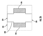
[0051]図2Aおよび図2Bは、本開示の態様による別の実施形態の電極構成を示している。第1の電極層220は、第1および第2の側部端子108、110(図1A)にそれぞれ接続され得る一対の対向するエッジ224、226を有する十字形状電極222を含み得る。図1Cは、第1の端部端子104に接続された第1の電極230と、第2の端部端子106に接続された第2の電極232とを含む第2の電極層228を示している。第1の電極230および/または第2の電極232は、電極230、232が電極層227の側部エッジ235、237まで延び、モノリシック本体102の少なくとも1つの側部表面239に沿って、それぞれの端部端子104、106(図1A)と接続するようなT字型電極であり得る。
[0051] FIGS. 2A and 2B illustrate another embodiment electrode configuration according to aspects of the present disclosure. The
[0052]図2Cは、交互する第1および第2の電極層220、228の電極の積み重ね233を示している。電極の積み重ね233は、Z方向140において厚さ242を有し得る。
[0052] Figure 2C shows an
[0053]モノリシック本体102(図1A)の厚さ138に対するZ方向140における電極の積み重ね233の厚さ242の比は、約0.4から約0.97の範囲であり得る。
[0054]再び図2Aを参照して示すように、十字形状電極122は、第1のオーバラップ領域234に沿って第1の電極230とオーバラップし、第2のオーバラップ領域236に沿って第2の電極232とオーバラップし得る。
[0053] The ratio of the
[0054] As shown again with reference to FIG. It may overlap with the
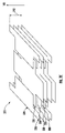
[0055]図3Aは、それぞれの追加リード648、650、および652を備えたバリスタデバイス660を備えた積み重ね構成で使用するための、一般に本開示の主題による多端子多層デバイス600の例示的な実施形態の外部斜視図を示している。本明細書でさらに論じられるように、図3Bは、用途図3Aの例示的な実施形態600の概略図を示す。
[0055] FIG. 3A illustrates an exemplary implementation of a
[0056]バリスタ660は、外部バリスタ端子662、664を有し得る。リード構成の構成を使用して、デバイス600およびバリスタ660を互いに平行に配置することができる。より具体的には、リード648、650、および652は、デバイス600の外部(コンデンサデバイス)端子604、608、および606にそれぞれ取り付けられ得る一方、リード648および652はそれぞれ、図示されるように、バリスタ660の外側(バリスタ)端子662および652に接続され得る。結果として得られる用途図3Aの構成は、オーバモールドされる可能性がある。
[0056] The
[0057]図3Bは、用途図3Aによって図示されるようなその接続/実装構成における、用途図3Aの例示的な実施形態600の概略図を一般的に示している。より具体的には、リード648、650、および652は、直列および並列コンデンサとそれぞれ接触して示されている。示された静電容量値は、限定的なものではなく、単なる例示として意図されている。バリスタ660は、同様に、例示されるように、リード648および652と接触しており、デバイス600と並列関係にある。示されているバリスタの特性は、限定的なものではなく、単なる例示として意図される。
[0057] FIG. 3B generally illustrates a schematic diagram of
[0058]図3Cは、本開示の態様による、コンデンサおよびバリスタ機能を有する統合構成要素の斜視図を示す。一般に、図3Cは、図3Aのデバイスを別の観点から示している。たとえば、図3Cの実施形態は、多層セラミックデバイスなどのデバイス600を下部に、バリスタ660を上部に提供する。そのような構成は、はんだ付けなどによって、デバイス600およびバリスタ660をともに組み合わせた後、表面実装デバイスとして使用することを可能にすることができる。それに加えて、図3Cに示される実施形態は、図3Aに示されるリードなしで提供される。しかしながら、そのような構成では、リードが使用されることもあると理解されたい。
[0058] FIG. 3C shows a perspective view of an integrated component having capacitor and varistor functionality, according to aspects of the present disclosure. Generally, FIG. 3C shows another view of the device of FIG. 3A. For example, the embodiment of Figure 3C provides a
[0059]例示されるように、デバイス600は、直列および並列コンデンサを収容するために、単一のデバイスソリューションを提供する。デバイス600は、デバイス600の隔離された領域における複数層の分割フィードスルー構成によって形成され得るような、2つの代表的なコンデンサ654および656を示す。
[0059] As illustrated,
[0060]本明細書で開示される例示的な実施形態のいずれかについて様々なサイズが実践され得るが、デバイス600およびバリスタ660は、標準的なMLCケースサイズ、たとえば、1206ケースサイズを表すと見なすことができる。もちろん、特定の用途に必要な、または所望されるように、様々なサイズが様々な実施形態において実践され得る。そのようなすべての変動、および、例示的な静電容量値の変動は、本開示の主題の精神および範囲を伴うことが意図される。
[0060] Although various sizes may be practiced for any of the exemplary embodiments disclosed herein,
[0061]本明細書の開示によって図示されるように、SMD構成で使用されるいくつかの実施形態では、本開示の主題は、プリント回路基板(PCB)上の複数のディスクリート構成要素の交換をもたらし、それによってスペースを節約し、場合によっては、インダクタンスを下げる。本開示のそのような例示的な実施形態のすべては、そのいくつかの使用において、オーバモールドされた3つのリード付き構成要素にパッケージされ得る。本開示の主題によれば、デバイスサイズの大幅な縮小が得られ、その結果、はんだ接合の数が減少し、それに応じて信頼性が向上する。 [0061] As illustrated by this disclosure, in some embodiments used in SMD configurations, the subject of this disclosure is the replacement of multiple discrete components on a printed circuit board (PCB). , thereby saving space and possibly lowering inductance. All such exemplary embodiments of the present disclosure, in some uses thereof, may be packaged in an overmolded three leaded component. The subject matter of the present disclosure provides a significant reduction in device size, resulting in a reduced number of solder joints and a corresponding increase in reliability.
[0062]図4は、本開示の態様による、コンデンサおよびバリスタ機能を有する統合構成要素を形成するための方法400のフローチャートである。一般に、方法400は、図1Aから図3Cを参照して上記で説明された統合構成要素100、200を参照して本明細書で説明される。しかしながら、開示された方法400は、任意の適切な統合構成要素を用いて実施され得ることが理解されるべきである。それに加えて、図4は、例示および議論の目的で特定の順序で実行されるステップを示しており、本明細書で論じられる方法は、特定の順序または配置に限定されない。本明細書で提供される開示を使用する当業者は、本開示の範囲から逸脱することなく、本明細書で開示される方法の様々なステップを省略、再配置、組合せ、および/または様々な方法で適合させることができることを理解するであろう。
[0062] FIG. 4 is a flowchart of a
[0063]方法400は、(402)において、たとえば、図1Aから図3Cを参照して上記で説明したように、分割フィードスルータイプの構造で一対のコンデンサを形成する電極を含む多層コンデンサ本体を提供することを含み得る。
[0063] The
[0064]この方法は、(404)において、たとえば、図1Aから図3Cを参照して上記で説明したように、一対のコンデンサが第1のアクティブ端子と第2のアクティブ端子との間に直列に接続されるように、多層コンデンサ本体の外部に第1のアクティブ端子および第2のアクティブ端子を形成することを含み得る。 [0064] The method includes at (404) a pair of capacitors in series between the first active terminal and the second active terminal, for example, as described above with reference to Figures 1A-3C. forming a first active terminal and a second active terminal external to the multilayer capacitor body such that they are connected to the .
[0065]この方法は、(406)において、ディスクリートバリスタの第1のバリスタ端子が第1のアクティブ端子に接続され、第2のバリスタ端子が第2のアクティブ端子に接続されるように、ディスクリートバリスタを多層コンデンサ本体と積み重ねることを含み得る。 [0065] At 406, the method includes the discrete varistor such that a first varistor terminal of the discrete varistor is connected to the first active terminal and a second varistor terminal is connected to the second active terminal. with the multilayer capacitor body.
[0066]開示された構成を達成する際における個々のステップは、その代表としてのみ意図されており、他に示された開示の一般的な性質を超える他の態様の必要な使用を示すものではないことを理解されたい。たとえば、当業者は、選択されたステップが、本開示の主題の所与の用途のために選択された特定の設計を生成するために実践され得ることを認識するであろう。
例
[0067]本開示の1つの例示的な実施形態によれば、統合構成要素は、おのおのが約475nFを示す第1および第2のコンデンサを有する。統合構成要素は、約22ボルトのクランプ電圧を有するディスクリートバリスタを含む。
[0066] Individual steps in achieving the disclosed configuration are intended only as representative thereof and are not intended to indicate the necessary use of other aspects beyond the general nature of the disclosure otherwise presented. It should be understood that no For example, one skilled in the art will recognize that selected steps may be implemented to produce a particular design selected for a given application of the disclosed subject matter.
example
[0067] According to one exemplary embodiment of the present disclosure, the integrated component has first and second capacitors each exhibiting approximately 475 nF. The integrated component includes a discrete varistor with a clamping voltage of approximately 22 volts.
[0068]本開示の1つの例示的な実施形態によれば、統合構成要素は、おのおのが約685nFを示す第1および第2のコンデンサを有する。統合構成要素は、約22ボルトのクランプ電圧を有するディスクリートバリスタを含む。 [0068] According to one exemplary embodiment of the present disclosure, the integrated component has first and second capacitors each exhibiting approximately 685 nF. The integrated component includes a discrete varistor with a clamping voltage of approximately 22 volts.
[0069]本開示の別の例示的な実施形態によれば、統合構成要素は、おのおのが約1μFを示す第1および第2のコンデンサを有する。統合構成要素は、約22ボルトのクランプ電圧を有するディスクリートバリスタを含む。
試験方法
[0070]以下のセクションは、多層セラミックコンデンサ、ディスクリートコンデンサ、および/または統合構成要素の様々な特性を判定するためにバリスタを試験するための例示的な方法を提供する。
[0069] According to another exemplary embodiment of the present disclosure, the integrated component has first and second capacitors each exhibiting about 1 μF. The integrated component includes a discrete varistor with a clamping voltage of approximately 22 volts.
Test method
[0070] The following sections provide exemplary methods for testing varistors to determine various characteristics of multilayer ceramic capacitors, discrete capacitors, and/or integrated components.
[0071]バリスタのクランプ電圧は、たとえば、Keithley 2410-C SMUのようなKeithley 2400シリーズソース測定ユニット(SMU)を使用して測定され得る。バリスタは、たとえばANSI規格C62.1にしたがって、8/20マイクロ秒の電流波(current wave)にさらされる場合がある。電流波は、1mAのピーク電流値を有し得る。ピーク電流値は、ピーク電流が、バリスタに対して、電圧を「クランプ」させるように選択され得る。電流は、ピーク電流値まで増加し、その後減衰し得る。「立ち上がり」期間は、電流パルスの開始から、電流がピーク電流値の90%に達するまでであり得る。「立ち上がり」時間は8マイクロ秒であり得る。「減衰時間」は、電流パルスの開始から、ピーク電流値の50%までであり得る。「減衰時間」は、20マイクロ秒であり得る。電流波の間のバリスタの両端の最大電圧として測定されたクランプ電圧。 [0071] The varistor clamp voltage can be measured using, for example, a Keithley 2400 series source-measure unit (SMU), such as the Keithley 2410-C SMU. A varistor may be subjected to a current wave of 8/20 microseconds, for example according to ANSI standard C62.1. The current wave may have a peak current value of 1 mA. The peak current value can be chosen such that the peak current causes the varistor to "clamp" the voltage. The current may increase to a peak current value and then decay. The "rise" period can be from the beginning of the current pulse until the current reaches 90% of the peak current value. The "rise" time can be 8 microseconds. A "decay time" can be from the onset of the current pulse to 50% of the peak current value. A "decay time" may be 20 microseconds. Clamp voltage measured as the maximum voltage across the varistor during the current wave.
[0072]多層コンデンサの静電容量は、たとえば、Keithley 2410-C SMUのような、Keithley 2400シリーズソース測定ユニット(SMU)を使用して測定され得る。たとえば、第1のコンデンサの第1の静電容量は、接地と、多層コンデンサの第1の外部端子との間で測定され得る。第2のコンデンサの第2の静電容量は、接地と、多層コンデンサの第2の外部端子との間で測定され得る。 [0072] The capacitance of a multilayer capacitor can be measured using a Keithley 2400 series source-measure unit (SMU), such as, for example, the Keithley 2410-C SMU. For example, a first capacitance of a first capacitor can be measured between ground and a first external terminal of the multilayer capacitor. A second capacitance of the second capacitor may be measured between ground and a second external terminal of the multilayer capacitor.
[0073]そのような本開示の主題は、その特定の実施形態に関して詳細に説明されているが、当業者は、前述の理解に達すると、そのような実施形態に対する変更、変形、および均等物を容易に生成できることが理解されよう。したがって、本開示の範囲は、限定ではなく例としてであり、主題の開示は、当業者に容易に明らかになるように、本開示の主題へのそのような修正、変形、および/または追加を含めることを排除しない。 [0073] Although such subject matter of the present disclosure has been described in detail with respect to specific embodiments thereof, modifications, variations, and equivalents to such embodiments will occur to those skilled in the art upon reaching the foregoing understanding. can be easily generated. Accordingly, the scope of the present disclosure is by way of example rather than limitation, and the subject disclosure may include such modifications, variations, and/or additions to the subject matter of the present disclosure, as will be readily apparent to those skilled in the art. Do not exclude inclusion.
Claims (27)
前記多層コンデンサの前記第1のアクティブ端子に接続された第1の外部バリスタ端子と、前記第2のアクティブ端子に接続された第2の外部バリスタ端子とを備えるディスクリートバリスタとを備える、統合構成要素。 A multilayer capacitor comprising a first active terminal, a second active terminal, at least one ground terminal, and a pair of capacitors connected in series between the first active terminal and the second active terminal. When,
an integrated component comprising a discrete varistor comprising a first external varistor terminal connected to said first active terminal of said multilayer capacitor and a second external varistor terminal connected to said second active terminal. .
複数の誘電体層を備える本体と、
前記本体内に配置され、前記第1のアクティブ端子に接続された第1の複数の電極層と、
前記本体内に配置され、前記第2のアクティブ端子に接続された第2の複数の電極層と、
前記少なくとも1つの接地端子に接続され、前記第1の複数の電極層および第2の複数の電極層のおのおのと容量結合されて、前記第1の複数の電極層と第3の複数の電極層との間に第1のコンデンサを、および、前記第2の複数の電極層と第3の複数の電極層との間に第2のコンデンサを形成する、前記第3の複数の電極層とを備える、請求項1に記載の統合構成要素。 The multilayer capacitor further comprises:
a body comprising a plurality of dielectric layers;
a first plurality of electrode layers disposed within the body and connected to the first active terminal;
a second plurality of electrode layers disposed within the body and connected to the second active terminal;
a first plurality of electrode layers and a third plurality of electrode layers connected to the at least one ground terminal and capacitively coupled to each of the first plurality of electrode layers and the second plurality of electrode layers; and said third plurality of electrode layers forming a first capacitor between said second plurality of electrode layers and a third plurality of electrode layers forming a second capacitor between said second plurality of electrode layers and a third plurality of electrode layers The integrated component of claim 1, comprising:
前記第3の複数の電極層は、前記第1のオーバラップ領域にほぼ等しい第2のオーバラップ領域に沿って、前記第2の複数の電極層とオーバラップする、請求項1に記載の統合構成要素。 the third plurality of electrode layers overlap the first plurality of electrode layers along a first overlap region;
2. The integration of claim 1, wherein said third plurality of electrode layers overlaps said second plurality of electrode layers along a second overlap area approximately equal to said first overlap area. Component.
一対のコンデンサを形成する電極を含む多層コンデンサ本体を提供するステップと、
前記一対のコンデンサが、第1のアクティブ端子と第2のアクティブ端子との間に直列に接続されるように、前記第1のアクティブ端子と、前記第2のアクティブ端子と、前記多層コンデンサ本体の外部の少なくとも1つの接地端子とを形成するステップと、
ディスクリートバリスタの第1のバリスタ端子が、前記第1のアクティブ端子に接続され、第2のバリスタ端子が、前記第2のアクティブ端子に接続されるように、前記ディスクリートバリスタを前記多層コンデンサ本体と積み重ねるステップとを備える、方法。 A method for forming an integrated component, comprising:
providing a multilayer capacitor body including electrodes forming a pair of capacitors;
the first active terminal, the second active terminal, and the multilayer capacitor body such that the pair of capacitors are connected in series between the first active terminal and the second active terminal; forming an external at least one ground terminal;
Stacking the discrete varistor with the multilayer capacitor body such that a first varistor terminal of the discrete varistor is connected to the first active terminal and a second varistor terminal is connected to the second active terminal A method comprising:
前記本体内に配置され、前記第1のアクティブ端子に接続された第1の複数の電極層を形成するステップと、
前記本体内に配置され、前記第2のアクティブ端子に接続された第2の複数の電極層を形成するステップとを備える、請求項15に記載の方法。 providing the multilayer capacitor body including electrodes forming the pair of capacitors,
forming a first plurality of electrode layers disposed within the body and connected to the first active terminal;
forming a second plurality of electrode layers disposed within the body and connected to the second active terminal.
前記第3の複数の電極層は、前記第1のオーバラップ領域にほぼ等しい第2のオーバラップ領域に沿って、前記第2の複数の電極層とオーバラップする、請求項15に記載の方法。 the third plurality of electrode layers overlap the first plurality of electrode layers along a first overlap region;
16. The method of claim 15, wherein the third plurality of electrode layers overlaps the second plurality of electrode layers along a second overlap area approximately equal to the first overlap area. .
Applications Claiming Priority (3)
| Application Number | Priority Date | Filing Date | Title |
|---|---|---|---|
| US201962838410P | 2019-04-25 | 2019-04-25 | |
| US62/838,410 | 2019-04-25 | ||
| PCT/US2020/028740 WO2020219357A1 (en) | 2019-04-25 | 2020-04-17 | Integrated component including a capacitor and discrete varistor |
Related Child Applications (1)
| Application Number | Title | Priority Date | Filing Date |
|---|---|---|---|
| JP2024111012A Division JP2024138420A (en) | 2019-04-25 | 2024-07-10 | Integrated components including capacitors and discrete varistors |
Publications (1)
| Publication Number | Publication Date |
|---|---|
| JP2022541088A true JP2022541088A (en) | 2022-09-22 |
Family
ID=72917269
Family Applications (1)
| Application Number | Title | Priority Date | Filing Date |
|---|---|---|---|
| JP2021563206A Pending JP2022541088A (en) | 2019-04-25 | 2020-04-17 | Integrated components including capacitors and discrete varistors |
Country Status (7)
| Country | Link |
|---|---|
| US (1) | US20200343051A1 (en) |
| JP (1) | JP2022541088A (en) |
| KR (1) | KR20210146452A (en) |
| CN (2) | CN117790188A (en) |
| DE (1) | DE112020002054T5 (en) |
| TW (1) | TW202109578A (en) |
| WO (1) | WO2020219357A1 (en) |
Families Citing this family (4)
| Publication number | Priority date | Publication date | Assignee | Title |
|---|---|---|---|---|
| WO2021235071A1 (en) * | 2020-05-21 | 2021-11-25 | パナソニックIpマネジメント株式会社 | Laminated varistor |
| JP2024507178A (en) * | 2021-02-25 | 2024-02-16 | ドングアン リテルヒューズ エレクロトニクス、カンパニー リミテッド | Surface mount metal oxide varistor device |
| CN117321713A (en) * | 2021-04-07 | 2023-12-29 | 基美电子公司 | Secondary injection molding film capacitor |
| US11348710B1 (en) | 2021-05-12 | 2022-05-31 | Dongguan Littelfuse Electronics Company Limited | Surface mount metal oxide varistor device |
Citations (4)
| Publication number | Priority date | Publication date | Assignee | Title |
|---|---|---|---|---|
| JPS5658809U (en) * | 1979-10-09 | 1981-05-20 | ||
| JPS619804U (en) * | 1984-06-22 | 1986-01-21 | 株式会社村田製作所 | Varistor for noise absorption |
| EP2947757A1 (en) * | 2014-05-21 | 2015-11-25 | Keko-Varicon d.o.o. | Electronic component with stacked elements |
| US20180226194A1 (en) * | 2017-02-06 | 2018-08-09 | Avx Corporation | Integrated Capacitor Filter and Integrated Capacitor Filter with Varistor Function |
Family Cites Families (24)
| Publication number | Priority date | Publication date | Assignee | Title |
|---|---|---|---|---|
| US4811164A (en) * | 1988-03-28 | 1989-03-07 | American Telephone And Telegraph Company, At&T Bell Laboratories | Monolithic capacitor-varistor |
| JPH02137212A (en) * | 1988-11-17 | 1990-05-25 | Murata Mfg Co Ltd | Composite electronic component |
| JPH03187203A (en) * | 1989-12-07 | 1991-08-15 | Siemens Ag | Varister with high capacity |
| JP2767014B2 (en) * | 1992-04-22 | 1998-06-18 | 株式会社村田製作所 | Noise filter |
| US5815367A (en) * | 1996-03-11 | 1998-09-29 | Murata Manufacturing Co., Ltd. | Layered capacitors having an internal inductor element |
| JP3631341B2 (en) * | 1996-10-18 | 2005-03-23 | Tdk株式会社 | Multilayer composite functional element and method for manufacturing the same |
| US7463474B2 (en) * | 2002-04-15 | 2008-12-09 | Avx Corporation | System and method of plating ball grid array and isolation features for electronic components |
| US7365428B2 (en) * | 2004-10-22 | 2008-04-29 | Intel Corporation | Array capacitor with resistive structure |
| KR100733816B1 (en) * | 2005-10-28 | 2007-07-02 | 주식회사 아모텍 | Laminated chip device |
| JP2008021850A (en) * | 2006-07-13 | 2008-01-31 | Murata Mfg Co Ltd | Multilayer capacitor |
| US20080165468A1 (en) * | 2007-01-05 | 2008-07-10 | Avx Corporation | Very low profile multilayer components |
| US20090147440A1 (en) * | 2007-12-11 | 2009-06-11 | Avx Corporation | Low inductance, high rating capacitor devices |
| AU2010100764A4 (en) * | 2009-07-23 | 2010-09-23 | Pakton Developments Pty Ltd | A safety device for electric fences |
| US8264816B2 (en) * | 2009-08-24 | 2012-09-11 | Kemet Electronics Corporation | Externally fused and resistively loaded safety capacitor |
| JP5062237B2 (en) * | 2009-11-05 | 2012-10-31 | Tdk株式会社 | Multilayer capacitor, mounting structure thereof, and manufacturing method thereof |
| JP5974490B2 (en) * | 2011-01-17 | 2016-08-23 | 株式会社村田製作所 | Electronic component element supply device |
| US9171672B2 (en) * | 2011-06-27 | 2015-10-27 | Kemet Electronics Corporation | Stacked leaded array |
| US8885324B2 (en) * | 2011-07-08 | 2014-11-11 | Kemet Electronics Corporation | Overvoltage protection component |
| KR101771728B1 (en) * | 2012-07-20 | 2017-08-25 | 삼성전기주식회사 | Laminated ceramic electronic parts and fabricating method thereof |
| JP6459717B2 (en) * | 2015-03-31 | 2019-01-30 | Tdk株式会社 | Multilayer ceramic capacitor |
| CN110520951B (en) * | 2017-03-29 | 2022-01-25 | 阿莫技术有限公司 | Electric shock protection element, manufacturing method thereof and portable electronic device with electric shock protection element |
| KR102136150B1 (en) * | 2017-05-02 | 2020-07-21 | 주식회사 아모텍 | Hybrid electric shock protection device and mobile electronic device with the same |
| KR102437806B1 (en) * | 2017-07-25 | 2022-08-30 | 삼성전기주식회사 | Composite electronic component and board for mounting the same |
| US10681814B2 (en) * | 2017-09-08 | 2020-06-09 | Kemet Electronics Corporation | High density multi-component packages |
-
2020
- 2020-04-16 US US16/850,142 patent/US20200343051A1/en active Pending
- 2020-04-17 JP JP2021563206A patent/JP2022541088A/en active Pending
- 2020-04-17 DE DE112020002054.1T patent/DE112020002054T5/en active Pending
- 2020-04-17 KR KR1020217038439A patent/KR20210146452A/en not_active Application Discontinuation
- 2020-04-17 CN CN202311638457.0A patent/CN117790188A/en active Pending
- 2020-04-17 CN CN202080031059.0A patent/CN113728407A/en active Pending
- 2020-04-17 WO PCT/US2020/028740 patent/WO2020219357A1/en active Application Filing
- 2020-04-24 TW TW109113740A patent/TW202109578A/en unknown
Patent Citations (4)
| Publication number | Priority date | Publication date | Assignee | Title |
|---|---|---|---|---|
| JPS5658809U (en) * | 1979-10-09 | 1981-05-20 | ||
| JPS619804U (en) * | 1984-06-22 | 1986-01-21 | 株式会社村田製作所 | Varistor for noise absorption |
| EP2947757A1 (en) * | 2014-05-21 | 2015-11-25 | Keko-Varicon d.o.o. | Electronic component with stacked elements |
| US20180226194A1 (en) * | 2017-02-06 | 2018-08-09 | Avx Corporation | Integrated Capacitor Filter and Integrated Capacitor Filter with Varistor Function |
Also Published As
| Publication number | Publication date |
|---|---|
| WO2020219357A1 (en) | 2020-10-29 |
| DE112020002054T5 (en) | 2022-01-27 |
| US20200343051A1 (en) | 2020-10-29 |
| CN113728407A (en) | 2021-11-30 |
| CN117790188A (en) | 2024-03-29 |
| TW202109578A (en) | 2021-03-01 |
| KR20210146452A (en) | 2021-12-03 |
Similar Documents
| Publication | Publication Date | Title |
|---|---|---|
| JP2022541088A (en) | Integrated components including capacitors and discrete varistors | |
| JP3900104B2 (en) | Antistatic parts | |
| KR101462798B1 (en) | Conductive paste composition for external electrode and multilayer ceramic components using the same | |
| US7710233B2 (en) | Electric multilayer component | |
| KR100799475B1 (en) | Surge absorption circuitry | |
| KR102552423B1 (en) | Dielectric powder and multilayered ceramic electronic components using the same | |
| JP2023169178A (en) | Integrated capacitor filter, and integrated capacitor filter with varistor function | |
| KR101719838B1 (en) | CONDUCTIVE RESIN COMPOSITION and MULTILAYER CERAMIC COMPONENTS HAVING THE SAME | |
| JP2024073627A (en) | Low inductance component | |
| JP2005203479A (en) | Static electricity countermeasure component | |
| CN112530699A (en) | Multilayer capacitor | |
| JP2024138420A (en) | Integrated components including capacitors and discrete varistors | |
| CN111146000B (en) | Multilayer ceramic capacitor | |
| TWI853922B (en) | Low inductance component and method for forming a low inductance component | |
| JPS63102218A (en) | Laminated multiterminal electronic component | |
| JP3078375B2 (en) | Multilayer ceramic capacitors | |
| JP3003369B2 (en) | Voltage-dependent nonlinear resistor porcelain element | |
| JPH05109507A (en) | Voltage dependent non linear resistor porcelain device | |
| JPH05251217A (en) | Voltage dependent non-linear resistor ceramic element | |
| JPH05251215A (en) | Voltage dependent non-linear resistor ceramic element |
Legal Events
| Date | Code | Title | Description |
|---|---|---|---|
| A524 | Written submission of copy of amendment under article 19 pct |
Free format text: JAPANESE INTERMEDIATE CODE: A525 Effective date: 20211214 |
|
| A621 | Written request for application examination |
Free format text: JAPANESE INTERMEDIATE CODE: A621 Effective date: 20220526 |
|
| A977 | Report on retrieval |
Free format text: JAPANESE INTERMEDIATE CODE: A971007 Effective date: 20230526 |
|
| A131 | Notification of reasons for refusal |
Free format text: JAPANESE INTERMEDIATE CODE: A131 Effective date: 20230609 |
|
| A521 | Request for written amendment filed |
Free format text: JAPANESE INTERMEDIATE CODE: A523 Effective date: 20230906 |
|
| A131 | Notification of reasons for refusal |
Free format text: JAPANESE INTERMEDIATE CODE: A131 Effective date: 20231102 |
|
| A521 | Request for written amendment filed |
Free format text: JAPANESE INTERMEDIATE CODE: A523 Effective date: 20240131 |
|
| A02 | Decision of refusal |
Free format text: JAPANESE INTERMEDIATE CODE: A02 Effective date: 20240322 |
|
| A521 | Request for written amendment filed |
Free format text: JAPANESE INTERMEDIATE CODE: A523 Effective date: 20240710 |
|
| A911 | Transfer to examiner for re-examination before appeal (zenchi) |
Free format text: JAPANESE INTERMEDIATE CODE: A911 Effective date: 20240718 |
|
| A912 | Re-examination (zenchi) completed and case transferred to appeal board |
Free format text: JAPANESE INTERMEDIATE CODE: A912 Effective date: 20240809 |