JP2022090891A - Light source apparatus, cooling method, and method for manufacturing goods - Google Patents
Light source apparatus, cooling method, and method for manufacturing goods Download PDFInfo
- Publication number
- JP2022090891A JP2022090891A JP2020203466A JP2020203466A JP2022090891A JP 2022090891 A JP2022090891 A JP 2022090891A JP 2020203466 A JP2020203466 A JP 2020203466A JP 2020203466 A JP2020203466 A JP 2020203466A JP 2022090891 A JP2022090891 A JP 2022090891A
- Authority
- JP
- Japan
- Prior art keywords
- light source
- flow path
- refrigerant
- valve
- refrigerator
- Prior art date
- Legal status (The legal status is an assumption and is not a legal conclusion. Google has not performed a legal analysis and makes no representation as to the accuracy of the status listed.)
- Pending
Links
- 238000001816 cooling Methods 0.000 title claims description 32
- 238000000034 method Methods 0.000 title claims description 14
- 238000004519 manufacturing process Methods 0.000 title claims description 11
- 239000003507 refrigerant Substances 0.000 claims description 103
- 239000000758 substrate Substances 0.000 claims description 40
- 230000003287 optical effect Effects 0.000 claims description 34
- 238000005286 illumination Methods 0.000 claims description 17
- 238000009826 distribution Methods 0.000 claims description 9
- 238000003860 storage Methods 0.000 claims description 6
- 230000008569 process Effects 0.000 claims description 5
- 230000001954 sterilising effect Effects 0.000 claims description 2
- 238000004659 sterilization and disinfection Methods 0.000 claims description 2
- 238000004381 surface treatment Methods 0.000 claims description 2
- 238000005259 measurement Methods 0.000 claims 2
- 239000007787 solid Substances 0.000 abstract description 3
- 239000002826 coolant Substances 0.000 abstract 2
- 238000010586 diagram Methods 0.000 description 21
- 230000007246 mechanism Effects 0.000 description 15
- 239000007788 liquid Substances 0.000 description 6
- 239000000463 material Substances 0.000 description 4
- QSHDDOUJBYECFT-UHFFFAOYSA-N mercury Chemical compound [Hg] QSHDDOUJBYECFT-UHFFFAOYSA-N 0.000 description 4
- 229910052753 mercury Inorganic materials 0.000 description 4
- RYGMFSIKBFXOCR-UHFFFAOYSA-N Copper Chemical compound [Cu] RYGMFSIKBFXOCR-UHFFFAOYSA-N 0.000 description 3
- 229910052802 copper Inorganic materials 0.000 description 3
- 239000010949 copper Substances 0.000 description 3
- 230000003111 delayed effect Effects 0.000 description 3
- 238000001459 lithography Methods 0.000 description 3
- 230000004048 modification Effects 0.000 description 3
- 238000012986 modification Methods 0.000 description 3
- 230000009471 action Effects 0.000 description 2
- 230000004913 activation Effects 0.000 description 2
- 230000007423 decrease Effects 0.000 description 2
- 238000010292 electrical insulation Methods 0.000 description 2
- 238000005530 etching Methods 0.000 description 2
- 239000004065 semiconductor Substances 0.000 description 2
- XLYOFNOQVPJJNP-UHFFFAOYSA-N water Substances O XLYOFNOQVPJJNP-UHFFFAOYSA-N 0.000 description 2
- 241000276498 Pollachius virens Species 0.000 description 1
- XAGFODPZIPBFFR-UHFFFAOYSA-N aluminium Chemical compound [Al] XAGFODPZIPBFFR-UHFFFAOYSA-N 0.000 description 1
- 229910052782 aluminium Inorganic materials 0.000 description 1
- 238000003491 array Methods 0.000 description 1
- 230000015572 biosynthetic process Effects 0.000 description 1
- 238000007664 blowing Methods 0.000 description 1
- 239000003795 chemical substances by application Substances 0.000 description 1
- 238000007796 conventional method Methods 0.000 description 1
- 238000005520 cutting process Methods 0.000 description 1
- 238000001514 detection method Methods 0.000 description 1
- 230000005611 electricity Effects 0.000 description 1
- 230000004907 flux Effects 0.000 description 1
- 239000004973 liquid crystal related substance Substances 0.000 description 1
- 238000012423 maintenance Methods 0.000 description 1
- 230000003647 oxidation Effects 0.000 description 1
- 238000007254 oxidation reaction Methods 0.000 description 1
- 238000004806 packaging method and process Methods 0.000 description 1
- 238000000206 photolithography Methods 0.000 description 1
- 238000012545 processing Methods 0.000 description 1
- 210000001747 pupil Anatomy 0.000 description 1
- 239000011347 resin Substances 0.000 description 1
- 229920005989 resin Polymers 0.000 description 1
- 238000009751 slip forming Methods 0.000 description 1
- 238000012360 testing method Methods 0.000 description 1
- 238000007740 vapor deposition Methods 0.000 description 1
- 239000002699 waste material Substances 0.000 description 1
Images


Classifications
-
- F—MECHANICAL ENGINEERING; LIGHTING; HEATING; WEAPONS; BLASTING
- F21—LIGHTING
- F21V—FUNCTIONAL FEATURES OR DETAILS OF LIGHTING DEVICES OR SYSTEMS THEREOF; STRUCTURAL COMBINATIONS OF LIGHTING DEVICES WITH OTHER ARTICLES, NOT OTHERWISE PROVIDED FOR
- F21V29/00—Protecting lighting devices from thermal damage; Cooling or heating arrangements specially adapted for lighting devices or systems
- F21V29/50—Cooling arrangements
- F21V29/70—Cooling arrangements characterised by passive heat-dissipating elements, e.g. heat-sinks
- F21V29/71—Cooling arrangements characterised by passive heat-dissipating elements, e.g. heat-sinks using a combination of separate elements interconnected by heat-conducting means, e.g. with heat pipes or thermally conductive bars between separate heat-sink elements
-
- F—MECHANICAL ENGINEERING; LIGHTING; HEATING; WEAPONS; BLASTING
- F21—LIGHTING
- F21V—FUNCTIONAL FEATURES OR DETAILS OF LIGHTING DEVICES OR SYSTEMS THEREOF; STRUCTURAL COMBINATIONS OF LIGHTING DEVICES WITH OTHER ARTICLES, NOT OTHERWISE PROVIDED FOR
- F21V29/00—Protecting lighting devices from thermal damage; Cooling or heating arrangements specially adapted for lighting devices or systems
- F21V29/50—Cooling arrangements
- F21V29/51—Cooling arrangements using condensation or evaporation of a fluid, e.g. heat pipes
- F21V29/52—Cooling arrangements using condensation or evaporation of a fluid, e.g. heat pipes electrically powered, e.g. refrigeration systems
-
- G—PHYSICS
- G03—PHOTOGRAPHY; CINEMATOGRAPHY; ANALOGOUS TECHNIQUES USING WAVES OTHER THAN OPTICAL WAVES; ELECTROGRAPHY; HOLOGRAPHY
- G03F—PHOTOMECHANICAL PRODUCTION OF TEXTURED OR PATTERNED SURFACES, e.g. FOR PRINTING, FOR PROCESSING OF SEMICONDUCTOR DEVICES; MATERIALS THEREFOR; ORIGINALS THEREFOR; APPARATUS SPECIALLY ADAPTED THEREFOR
- G03F7/00—Photomechanical, e.g. photolithographic, production of textured or patterned surfaces, e.g. printing surfaces; Materials therefor, e.g. comprising photoresists; Apparatus specially adapted therefor
- G03F7/70—Microphotolithographic exposure; Apparatus therefor
- G03F7/70008—Production of exposure light, i.e. light sources
-
- F—MECHANICAL ENGINEERING; LIGHTING; HEATING; WEAPONS; BLASTING
- F21—LIGHTING
- F21V—FUNCTIONAL FEATURES OR DETAILS OF LIGHTING DEVICES OR SYSTEMS THEREOF; STRUCTURAL COMBINATIONS OF LIGHTING DEVICES WITH OTHER ARTICLES, NOT OTHERWISE PROVIDED FOR
- F21V23/00—Arrangement of electric circuit elements in or on lighting devices
- F21V23/003—Arrangement of electric circuit elements in or on lighting devices the elements being electronics drivers or controllers for operating the light source, e.g. for a LED array
- F21V23/004—Arrangement of electric circuit elements in or on lighting devices the elements being electronics drivers or controllers for operating the light source, e.g. for a LED array arranged on a substrate, e.g. a printed circuit board
-
- F—MECHANICAL ENGINEERING; LIGHTING; HEATING; WEAPONS; BLASTING
- F21—LIGHTING
- F21V—FUNCTIONAL FEATURES OR DETAILS OF LIGHTING DEVICES OR SYSTEMS THEREOF; STRUCTURAL COMBINATIONS OF LIGHTING DEVICES WITH OTHER ARTICLES, NOT OTHERWISE PROVIDED FOR
- F21V29/00—Protecting lighting devices from thermal damage; Cooling or heating arrangements specially adapted for lighting devices or systems
- F21V29/50—Cooling arrangements
- F21V29/502—Cooling arrangements characterised by the adaptation for cooling of specific components
- F21V29/503—Cooling arrangements characterised by the adaptation for cooling of specific components of light sources
-
- F—MECHANICAL ENGINEERING; LIGHTING; HEATING; WEAPONS; BLASTING
- F21—LIGHTING
- F21V—FUNCTIONAL FEATURES OR DETAILS OF LIGHTING DEVICES OR SYSTEMS THEREOF; STRUCTURAL COMBINATIONS OF LIGHTING DEVICES WITH OTHER ARTICLES, NOT OTHERWISE PROVIDED FOR
- F21V29/00—Protecting lighting devices from thermal damage; Cooling or heating arrangements specially adapted for lighting devices or systems
- F21V29/50—Cooling arrangements
- F21V29/56—Cooling arrangements using liquid coolants
-
- G—PHYSICS
- G03—PHOTOGRAPHY; CINEMATOGRAPHY; ANALOGOUS TECHNIQUES USING WAVES OTHER THAN OPTICAL WAVES; ELECTROGRAPHY; HOLOGRAPHY
- G03F—PHOTOMECHANICAL PRODUCTION OF TEXTURED OR PATTERNED SURFACES, e.g. FOR PRINTING, FOR PROCESSING OF SEMICONDUCTOR DEVICES; MATERIALS THEREFOR; ORIGINALS THEREFOR; APPARATUS SPECIALLY ADAPTED THEREFOR
- G03F7/00—Photomechanical, e.g. photolithographic, production of textured or patterned surfaces, e.g. printing surfaces; Materials therefor, e.g. comprising photoresists; Apparatus specially adapted therefor
- G03F7/70—Microphotolithographic exposure; Apparatus therefor
- G03F7/70008—Production of exposure light, i.e. light sources
- G03F7/7005—Production of exposure light, i.e. light sources by multiple sources, e.g. light-emitting diodes [LED] or light source arrays
-
- G—PHYSICS
- G03—PHOTOGRAPHY; CINEMATOGRAPHY; ANALOGOUS TECHNIQUES USING WAVES OTHER THAN OPTICAL WAVES; ELECTROGRAPHY; HOLOGRAPHY
- G03F—PHOTOMECHANICAL PRODUCTION OF TEXTURED OR PATTERNED SURFACES, e.g. FOR PRINTING, FOR PROCESSING OF SEMICONDUCTOR DEVICES; MATERIALS THEREFOR; ORIGINALS THEREFOR; APPARATUS SPECIALLY ADAPTED THEREFOR
- G03F7/00—Photomechanical, e.g. photolithographic, production of textured or patterned surfaces, e.g. printing surfaces; Materials therefor, e.g. comprising photoresists; Apparatus specially adapted therefor
- G03F7/70—Microphotolithographic exposure; Apparatus therefor
- G03F7/70058—Mask illumination systems
- G03F7/70075—Homogenization of illumination intensity in the mask plane by using an integrator, e.g. fly's eye lens, facet mirror or glass rod, by using a diffusing optical element or by beam deflection
-
- G—PHYSICS
- G03—PHOTOGRAPHY; CINEMATOGRAPHY; ANALOGOUS TECHNIQUES USING WAVES OTHER THAN OPTICAL WAVES; ELECTROGRAPHY; HOLOGRAPHY
- G03F—PHOTOMECHANICAL PRODUCTION OF TEXTURED OR PATTERNED SURFACES, e.g. FOR PRINTING, FOR PROCESSING OF SEMICONDUCTOR DEVICES; MATERIALS THEREFOR; ORIGINALS THEREFOR; APPARATUS SPECIALLY ADAPTED THEREFOR
- G03F7/00—Photomechanical, e.g. photolithographic, production of textured or patterned surfaces, e.g. printing surfaces; Materials therefor, e.g. comprising photoresists; Apparatus specially adapted therefor
- G03F7/70—Microphotolithographic exposure; Apparatus therefor
- G03F7/70058—Mask illumination systems
- G03F7/7015—Details of optical elements
-
- G—PHYSICS
- G03—PHOTOGRAPHY; CINEMATOGRAPHY; ANALOGOUS TECHNIQUES USING WAVES OTHER THAN OPTICAL WAVES; ELECTROGRAPHY; HOLOGRAPHY
- G03F—PHOTOMECHANICAL PRODUCTION OF TEXTURED OR PATTERNED SURFACES, e.g. FOR PRINTING, FOR PROCESSING OF SEMICONDUCTOR DEVICES; MATERIALS THEREFOR; ORIGINALS THEREFOR; APPARATUS SPECIALLY ADAPTED THEREFOR
- G03F7/00—Photomechanical, e.g. photolithographic, production of textured or patterned surfaces, e.g. printing surfaces; Materials therefor, e.g. comprising photoresists; Apparatus specially adapted therefor
- G03F7/70—Microphotolithographic exposure; Apparatus therefor
- G03F7/708—Construction of apparatus, e.g. environment aspects, hygiene aspects or materials
- G03F7/70858—Environment aspects, e.g. pressure of beam-path gas, temperature
- G03F7/70883—Environment aspects, e.g. pressure of beam-path gas, temperature of optical system
- G03F7/70891—Temperature
-
- F—MECHANICAL ENGINEERING; LIGHTING; HEATING; WEAPONS; BLASTING
- F21—LIGHTING
- F21Y—INDEXING SCHEME ASSOCIATED WITH SUBCLASSES F21K, F21L, F21S and F21V, RELATING TO THE FORM OR THE KIND OF THE LIGHT SOURCES OR OF THE COLOUR OF THE LIGHT EMITTED
- F21Y2105/00—Planar light sources
- F21Y2105/10—Planar light sources comprising a two-dimensional array of point-like light-generating elements
- F21Y2105/14—Planar light sources comprising a two-dimensional array of point-like light-generating elements characterised by the overall shape of the two-dimensional array
- F21Y2105/16—Planar light sources comprising a two-dimensional array of point-like light-generating elements characterised by the overall shape of the two-dimensional array square or rectangular, e.g. for light panels
-
- F—MECHANICAL ENGINEERING; LIGHTING; HEATING; WEAPONS; BLASTING
- F21—LIGHTING
- F21Y—INDEXING SCHEME ASSOCIATED WITH SUBCLASSES F21K, F21L, F21S and F21V, RELATING TO THE FORM OR THE KIND OF THE LIGHT SOURCES OR OF THE COLOUR OF THE LIGHT EMITTED
- F21Y2115/00—Light-generating elements of semiconductor light sources
- F21Y2115/10—Light-emitting diodes [LED]
Landscapes
- Engineering & Computer Science (AREA)
- Physics & Mathematics (AREA)
- General Physics & Mathematics (AREA)
- General Engineering & Computer Science (AREA)
- Health & Medical Sciences (AREA)
- Toxicology (AREA)
- Life Sciences & Earth Sciences (AREA)
- Atmospheric Sciences (AREA)
- Environmental & Geological Engineering (AREA)
- Epidemiology (AREA)
- Public Health (AREA)
- Microelectronics & Electronic Packaging (AREA)
- Led Device Packages (AREA)
- Exposure And Positioning Against Photoresist Photosensitive Materials (AREA)
- Cooling Or The Like Of Electrical Apparatus (AREA)
- Cooling Or The Like Of Semiconductors Or Solid State Devices (AREA)
Abstract
Description
本発明は、光源装置、冷却方法、及び物品の製造方法に関する。 The present invention relates to a light source device, a cooling method, and a method for manufacturing an article.
半導体デバイスやフラットパネルディスプレイ(FPD)等のデバイスを製造する際のフォトリソグラフィ工程において、マスクのパターンを基板に転写する露光装置が用いられている。露光装置の光源には、例えば、水銀ランプが用いられているが、近年では水銀ランプよりも省エネルギーである発光ダイオード(LED:Light Emitting Diode)へ置換することが期待されている。LEDは、回路に電流を流してから光の出力が安定するまでの時間が短く、水銀ランプのように常時発光させる必要がないため、長寿命でもある。 In a photolithography process when manufacturing a device such as a semiconductor device or a flat panel display (FPD), an exposure device that transfers a mask pattern to a substrate is used. For example, a mercury lamp is used as a light source of an exposure apparatus, but in recent years, it is expected to replace it with a light emitting diode (LED: Light Emitting Diode), which is more energy-saving than a mercury lamp. An LED has a long life because it takes a short time from when a current is passed through a circuit until the light output stabilizes, and it is not necessary to constantly emit light unlike a mercury lamp.
LEDは、チップ1個あたりの輝度は小さいため、所望の照度を得るためには、電気基板に複数のLEDチップを配列した光源を用いる必要がある。水銀ランプと同等の照度を得るために必要なLEDチップの個数は、例えば、数千個程度である。LEDチップを発光させる際には、LEDチップの温度が上昇するためLEDチップを冷却する必要がある。 Since the brightness of each LED is small, it is necessary to use a light source in which a plurality of LED chips are arranged on an electric substrate in order to obtain a desired illuminance. The number of LED chips required to obtain the same illuminance as a mercury lamp is, for example, about several thousand. When the LED chip emits light, the temperature of the LED chip rises, so it is necessary to cool the LED chip.
LEDチップの寿命(LEDチップの点灯時間)は、LEDチップが発光する際の温度に依存しており、LEDチップの温度が高いほどLEDチップの寿命が短くなる。ここで、例えば、複数のLEDチップを電気基板に配列した光源(LED光源モジュール)を用いた露光装置において、一部のLEDチップが寿命となり、所望の光量を得ることができない場合には、電気基板ごと新しいものに交換する必要がある。即ち、複数のLEDチップで温度のバラつきがある場合には、LED光源モジュールの交換タイミングが早くなってしまうおそれがある。特許文献1には、1次元的に配列された複数のLEDチップに対して2つの流路を設け、互いに反対方向に冷媒を流すことで、複数のLEDチップを均一に冷却することができる内容が開示されている。 The life of the LED chip (lighting time of the LED chip) depends on the temperature at which the LED chip emits light, and the higher the temperature of the LED chip, the shorter the life of the LED chip. Here, for example, in an exposure device using a light source (LED light source module) in which a plurality of LED chips are arranged on an electric substrate, when some of the LED chips have reached the end of their useful life and a desired amount of light cannot be obtained, electricity is used. It is necessary to replace the entire board with a new one. That is, if there is a temperature variation among a plurality of LED chips, the replacement timing of the LED light source module may be earlier. Patent Document 1 provides two flow paths for a plurality of LED chips arranged one-dimensionally, and allows a plurality of LED chips to be uniformly cooled by flowing a refrigerant in opposite directions. Is disclosed.
特許文献1のような構成の流路を形成した場合には、流路の幅が狭くなるため、冷媒の冷却力が低下するおそれがある。また、LEDチップが2次元的に配列されている場合には、複数のLEDチップを均一に冷却するために多くの流路を形成する必要がある。冷媒の冷却力を向上させたい場合には、流路の幅が狭くならないように、流路を可能な限りシンプルに構成することが望ましい。例えば、流路を1つにすることで、冷媒の単位時間あたりの流速を向上させることができる。しかしながら、その場合には、流路の下流側ではLEDチップを冷却する冷却力が低くなってしまうため、複数のLEDチップを均一に冷却することができない。その結果、複数のLEDチップを均一に冷却した場合に比べてLED光源モジュールの交換タイミングが早くなってしまう。 When a flow path having the configuration as in Patent Document 1 is formed, the width of the flow path becomes narrow, so that the cooling power of the refrigerant may decrease. Further, when the LED chips are arranged two-dimensionally, it is necessary to form many channels in order to uniformly cool the plurality of LED chips. When it is desired to improve the cooling power of the refrigerant, it is desirable to configure the flow path as simple as possible so that the width of the flow path is not narrowed. For example, by making one flow path, the flow velocity of the refrigerant per unit time can be improved. However, in that case, since the cooling power for cooling the LED chips is low on the downstream side of the flow path, it is not possible to uniformly cool the plurality of LED chips. As a result, the replacement timing of the LED light source module becomes earlier than when the plurality of LED chips are uniformly cooled.
そこで、本発明は、LED光源モジュールの交換タイミングを遅らせるために有利な光源装置を提供することを目的とする。 Therefore, an object of the present invention is to provide an advantageous light source device for delaying the replacement timing of the LED light source module.
上記目的を達成するために、本発明の一側面としての光源装置は、電気基板と、前記電気基板に配列されている固体発光素子と、前記電気基板に接触して配置され、内部に形成された流路を冷媒が流れるヒートシンクと、前記流路において冷媒が流れる方向を反対の方向に切り替える切り替え手段と、を有することを特徴とする。 In order to achieve the above object, the light source device as one aspect of the present invention is formed in an electric substrate, a solid light emitting element arranged on the electric substrate, and arranged in contact with the electric substrate. It is characterized by having a heat sink through which the refrigerant flows in the flow path, and a switching means for switching the direction in which the refrigerant flows in the flow path in the opposite direction.
本発明によれば、LED光源モジュールの交換タイミングを遅らせるために有利な光源装置を提供することができる。 According to the present invention, it is possible to provide an advantageous light source device for delaying the replacement timing of the LED light source module.
以下に、本発明の好ましい実施形態を添付の図面に基づいて詳細に説明する。尚、各図において、同一の部材については同一の参照番号を付し、重複する説明は省略する。 Hereinafter, preferred embodiments of the present invention will be described in detail with reference to the accompanying drawings. In addition, in each figure, the same reference number is given to the same member, and duplicate description is omitted.
<第1実施形態>
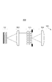
図1を参照して、本実施形態における光源装置10について説明する。図1(a)は、光源装置10の全体の構成を示す図である。光源装置10は、LEDチップ11(固体発光素子)、電気基板12、電源13、制御部14を有する。電気基板12に複数のLEDチップが配列されたものをLED光源モジュールとも称する。更に光源装置10は、LEDチップ11を冷却するために、ヒートシンク15、冷凍機16(チラーとも呼ばれる)、切り替え機構17(切り替え手段)を有する。本実施形態では、LEDチップ11が配列される平面をXY平面、XY平面に垂直な方向をZ軸方向と定義する。
<First Embodiment>
The
図1(b)は、光源装置10の発光面の構成を示す図である。電気基板12には銅配線が実装されており、LEDチップ11を発光させるための回路が形成されている。回路の配線に使用される材質は銅以外の材質でも良い。回路に電流が流れることで、LEDチップ11から所定の波長の光が出力される。本実施形態では、複数のLEDチップ11が二次元に配列されている例について説明するが、これに限らず、LEDチップ11が一次元に配列されていても良い。電源13は、電気基板12の回路に接続されており、LEDチップ11を発光させるための電力を供給する。電源13は、制御部14に接続されており、不図示の上位の制御系からの指令に従ってLEDチップ11の照度等を制御する。
FIG. 1B is a diagram showing a configuration of a light emitting surface of the
LEDチップ11の発光に伴いLEDチップ11が発熱し、LEDチップ11の温度が上昇する。LEDチップ11の発光に伴い生じた熱を冷却するための光源装置10の構成について説明する。本実施形態では、光源装置10に冷媒を流すことにより、冷媒と電気基板12の熱交換を行う。この熱交換により、LEDチップ11を冷却することができる。熱交換の効率を上げるために、熱伝導率が高い素材を電気基板2に用いることが好ましい。電気基板2の材質としては、例えば、熱伝導率が高い銅やアルミニウムを用いると良い。冷媒には、例えば、冷却力が優れている水を主成分とする液体や、電気絶縁性に優れたオイルを主成分する液体が用いられ得る。本実施形態では、液体によりLEDチップ11を冷却する例について説明するが、これに限らず、例えば、温度の低い気体を吹き付けることによる空冷によりLEDチップ11を冷却しても良い。
The
図1(c)は、光源装置10のヒートシンク15の断面図を示す図である。ヒートシンク15は、LEDチップ11が発光した際に放出される熱を吸収する。ヒートシンク15は、電気基板12の裏面(LEDチップ11が配列されている面とは反対の面)に接触して保持されている。ヒートシンク15の内部には、冷媒を流すための流路18が直線的に設けられている。流路18は、配管を介して冷凍機16と接続されており、流路18から排出された冷媒を冷却するために冷凍機16に送られる。冷凍機16は、冷媒を冷却して一定温度(例えば20℃)に制御し、再び電気基板12と熱交換を行うように冷媒を循環させる。LEDチップ11を冷却する冷媒には、例えば、冷却力が優れている水を主成分とする液体や、電気絶縁性に優れた不活性オイルを主成分とする液体が用いられ得る。
FIG. 1 (c) is a diagram showing a cross-sectional view of the
本実施形態では、ヒートシンク15と冷凍機16との間に切り替え機構17を設ける等によって実現する切り替え手段が備えられており、切り替え手段により流路18において冷媒が流れる方向を切り替えることが可能な構成となっている。切り替え手段の具体的な例については、後述する実施例1~4で説明する。
In the present embodiment, a switching means realized by providing a
(LEDチップの寿命)
図2を参照して、複数のLEDチップ11の温度のバラつきによる影響について説明する。図2は、光源装置10における複数のLEDチップ11の温度分布を示した図である。図2のグラフにおいて実線で示す温度は、X軸方向のマイナス側からプラス側へと冷媒が流路18を流れる場合の温度分布である。また、図2のグラフにおいて点線で示す温度は、X軸方向のプラス側からマイナス側へと冷媒が流路18を流れる場合におけるLEDチップ11の温度分布である。両者共に、流路18の冷媒入口付近では、LEDチップ11の温度は50℃となるが、冷媒が流路18を流れるにつれて、LEDチップ11から熱を吸収して徐々に冷却力が下がっていき、流路18の出口付近では、LEDチップ11の温度は100℃となる。流路18は、入口と出口が直線的に結ばれており、Y軸方向に温度分布はほとんど発生しない構造であることを想定しているが、これに限らない。
(Life of LED chip)
With reference to FIG. 2, the influence of the temperature variation of the plurality of
次に、LEDチップ11の温度と寿命の関係性について説明をする。ここで、LEDチップ11の発光面の温度をジャンクション温度と呼ぶ。LEDチップ11の寿命は、アレニウスの式を用いて式(1)のように予測することができる。Lは寿命、Aは定数、Eは活性化エネルギー、Kはボルツマン定数、Tはジャンクション温度である。
L=A×exp(E/KT)・・・(1)
Next, the relationship between the temperature and the life of the
L = A × exp (E / KT) ・ ・ ・ (1)
式(1)より、活性化エネルギー(即ち、電流)が同じである場合、ジャンクション温度のみがLEDチップの寿命の長さに影響し、ジャンクション温度が低いほどLEDチップ11の寿命は長くなる。図3は、LEDチップ11の温度と寿命の関係の一例を示すグラフである。図3で示すグラフの横軸はLEDチップ11の温度であり、縦軸はLEDチップ11がその温度で発光し続けた際の寿命である。図3では、LEDチップ11が50℃で発光し続けた際には、寿命が23000時間であるのに対し、LEDチップ11が100℃で発光し続けた際には、寿命が14000時間となってしまう。図2の例に当てはめると、流路18の冷媒入口付近に配列されているLEDチップ11の寿命よりも流路18の冷媒出口付近に配列されているLEDチップ11の寿命が大幅に短くなってしまう。
From the formula (1), when the activation energy (that is, the current) is the same, only the junction temperature affects the life of the LED chip, and the lower the junction temperature, the longer the life of the
一部のLEDチップ11が寿命となり光源装置10の目標照度を達成できなくなった場合には、LEDチップを新しいものに取り換えるために電気基板12ごと新しいものに取り換えることが一般的である。このように電気基板12ごとLEDチップ11を交換する場合には、複数のLEDチップ11のうち最も寿命が短いもので律速されることになる。流路18を一方向のみに冷媒が流れる場合には、LEDチップの多くを寿命になるまで使用することができない。
When a part of the LED chips 11 has reached the end of its useful life and the target illuminance of the
冷媒が流れる方向を反対方向に反転させた場合、流路18の入口側の温度と出口側の温度分布が反転し、先の説明で流路18の冷媒出口付近に配列されたLEDチップ11の寿命が長くなる。流路を反転させる回数やタイミングについては、最初に冷媒が流れている方向に冷媒が流れているときのLEDチップ11の点灯時間と、その方向と反対方向に冷媒が流れているときのLEDチップ11の点灯時間が等しい場合に最も寿命が長くなる。その時の寿命時間は、50℃と100℃の平均値の75℃での寿命時間である18500時間程度となる。冷媒が流れる方向を1回のみ反転させる場合には、75℃での寿命時間の半分の時間である9250時間に点灯時間が達した時に、LED光源モジュールの交換タイミングを最も遅い18500時間程度に遅らせることができる。即ち、LEDチップ11の寿命時間内で一回でも流路を反転させることで、14000時間程度であった寿命を最大18500時間程度まで伸ばすことが可能となる。
When the direction in which the refrigerant flows is reversed in the opposite direction, the temperature on the inlet side and the temperature distribution on the outlet side of the
冷媒が流れる方向を反転する回数は上記のように1回でも良いが、複数回行っても良く、一定時間ごと(例えば、100時間ごと)に反転させても良い。また、例えば、光源装置10を露光装置に用いる場合には、露光装置のメンテナンス等により露光装置がダウンしている間に冷媒が流れる方向の反転作業を実施することで、装置の稼働率を下げることなく、複数のLEDチップ11を無駄なく使用できる。また、冷媒が流れる方向を切り替える際には、熱交換後の冷媒が冷凍機16で冷却される前に逆流することになる。これを防ぐために、LEDチップ11が消灯しているときに冷媒が流れる方向を反転する作業を行うことが好ましい。
The number of times that the direction in which the refrigerant flows is reversed may be once as described above, but may be performed a plurality of times, or may be reversed at regular time intervals (for example, every 100 hours). Further, for example, when the
(実施例1)
実施例1では、切り替え機構17(切り替え手段)が4つのバルブで構成されており、流路18において冷媒が流れる方向を第1方向から第1方向とは反対方向である第2方向に切り替え可能である例について説明する。図4は、実施例1における光源装置10を示す図である。冷凍機16の冷媒出口(図中OUTで表示)には、配管P41がつながっている。配管P41は途中で二股に分かれ、切り替え機構17内部のバルブV1(第1のバルブ)、バルブV2(第2のバルブ)につながっている。また、冷凍機17の冷媒入口(図中INで表示)には、配管P43が接続されており、二股に分かれてそれぞれバルブV3(第3のバルブ)、バルブV4(第4のバルブ)に接続されている。図4では、切り替え機構17の内部で配管が分岐しているよう図示しているが、切り替え機構17の外部に分岐があっても良い。
(Example 1)
In the first embodiment, the switching mechanism 17 (switching means) is composed of four valves, and the direction in which the refrigerant flows in the
更に、バルブV1とバルブV3には、それぞれ配管P42と配管P421が接続されており、配管P421は、配管P42に合流するように接続されている。一方、バルブV2とバルブV4には、それぞれ配管P422と配管P44が接続されており、配管P422は、配管P44と合流する様に接続されている。配管P42、配管P44は、ヒートシンク15の内部における流路18の異なる端部にそれぞれ接続されている。また、制御部14は切り替え機構17と接続され、バルブの操作を制御しても良い。
Further, the pipe P42 and the pipe P421 are connected to the valve V1 and the valve V3, respectively, and the pipe P421 is connected so as to join the pipe P42. On the other hand, the pipe P422 and the pipe P44 are connected to the valve V2 and the valve V4, respectively, and the pipe P422 is connected so as to join the pipe P44. The pipe P42 and the pipe P44 are connected to different ends of the
本実施例におけるバルブV1~バルブV4の操作について説明する。バルブV1とバルブV4の開閉状態は常に同じ状態、バルブV2とバルブV3の開閉状態も常に同じ状態で運用される。バルブV1、バルブV4が開いている状態では、バルブV2、バルブV3は閉じている状態となり、バルブV1、バルブV4が閉じている状態では、バルブV2、バルブV3は開いている状態となるよう運用する。以上のように運用することで、流路18内の冷媒が流れる方向を反転することができる構造となっている。
The operation of valves V1 to V4 in this embodiment will be described. The open / closed state of the valve V1 and the valve V4 is always the same, and the open / closed state of the valve V2 and the valve V3 is always the same. When the valves V1 and V4 are open, the valves V2 and V3 are closed, and when the valves V1 and V4 are closed, the valves V2 and V3 are open. do. By operating as described above, the structure is such that the direction in which the refrigerant flows in the
バルブの操作については、手動により行われても良いし、電動のバルブとして4つのバルブが連動して駆動するように制御部14によって行われても良い。また、冷媒が流れる方向の反転作業を行うタイミングについて、制御部14により所定の時間経過した後に切り替わるように制御されても良いし、人為的にタイミングを決定しても良い。
The operation of the valves may be performed manually, or may be performed by the
(実施例2)
実施例2では、切り替え機構17(切り替え手段)が流路18において冷媒が流れる方向を第1方向から第1方向とは反対方向である第2方向に切り替えることができる電磁弁51を備えている例について説明する。図5は、実施例2における光源装置10を示す図である。電磁弁51は、配管P1、P3と配管P2とP4を接続するための4つのポートを有している。電磁弁51は、2つのポジションをとることができ、配管P1とP2、及び配管P3とP4を接続させるポジションと、配管P1とP4、及び配管P3とP2を接続させるポジションをとることができる。また、電磁弁51は、制御部14と接続されており、切り替え機構17の電磁弁51を駆動するための指令及び駆動を制御部14により制御される。
(Example 2)
In the second embodiment, the switching mechanism 17 (switching means) includes a
電磁弁51が一方のポジションをとる場合には、冷却器16から排出された冷媒が配管P1、配管P2を通り流路18に導かれ、配管P4、配管P3を通って再び冷却器16へと戻る。電磁弁51が他方のポジションをとる場合には、冷却器16から排出された冷媒が配管P1、配管P4を通り流路18に導かれ、配管P2、配管P3を通って再び冷却器16へと戻る。このように電磁弁51のポジションを変更することで、流路18内の冷媒が流れる方向を反転することができる構造となっている。
When the
電磁弁の駆動については、電動の電磁弁として制御部14によって行われることを想定して説明したが、手動により行われても良い。また、冷媒が流れる方向の反転作業を行うタイミングについて、制御部14により所定の時間経過した後に切り替わるように制御されても良いし、人為的にタイミングを決定しても良い。
The driving of the solenoid valve has been described assuming that it is performed by the
(実施例3)
実施例3では、切り替え手段としての切り替え機構17を有していない例について説明する。実施例3では、配管の接続先を人為的に入れ替えることで冷媒が流れる方向を第1方向から第1方向とは反対方向である第2方向に切り替えることができる切り替え手段を有する。図6は、実施例3における光源装置10を示す図である。図6(a)は切り替えを行う前の光源装置10であり、図6(b)は切り替えを行った後の光源装置10である。
(Example 3)
In the third embodiment, an example in which the
図6(a)では、冷凍器16から冷媒が排出される冷媒出口(図中OUTで表示)には継手Faが接続されている。継手Faには配管P2の一端が接続されており、配管P2の他端は流路18の一端へと接続されている。流路18の他端には、配管P4が接続されており、配管P4の先端部の継手Fbは、冷凍機16の入口(図中INで表示)に接続されている。つまり、冷凍器16から出た冷媒は配管P2を通って流路を通り、配管P4を通って冷凍器16へと戻ってくる。
In FIG. 6A, the joint Fa is connected to the refrigerant outlet (indicated by OUT in the figure) from which the refrigerant is discharged from the
図6(b)では、図6(a)の状態から配管P2と配管P4を繋ぎ変えている図である。継手Fbには配管P4の一端が接続されており、配管P4の他端は流路18の一端へと接続されている。流路18の他端には、配管P2が接続されており、配管P2の先端部の継手Faは、冷凍機16の入口(図中INで表示)に接続されている。つまり、冷凍器16から出た冷媒は配管P4を通って流路を通り、配管P2を通って冷凍器16へと戻ってくる。
FIG. 6B is a diagram in which the pipe P2 and the pipe P4 are reconnected from the state of FIG. 6A. One end of the pipe P4 is connected to the joint Fb, and the other end of the pipe P4 is connected to one end of the
本実施例では、手動で配管を繋ぎ替えることで、冷媒が流れる方向を切り替えることができる。継手Fa、継手Fbは同じ型の物を用いて、繋ぎ替えた時に冷凍機16のINとOUTの両方に共通化されているとよい。また、不図示であるが、繋ぎ替え作業時に冷媒が漏れないようにストップバルブを設置しても良い。さらに、継手を差し込むだけで接続が可能な特殊な継手を用いることで、切り替え時の利便性が向上する。
In this embodiment, the direction in which the refrigerant flows can be switched by manually reconnecting the pipes. It is preferable that the joint Fa and the joint Fb are of the same type and are common to both IN and OUT of the
(実施例4)
実施例4では、切り替え機構17(切り替え手段)が、流路18において冷媒が流れる方向を第1方向から第1方向とは反対方向である第2方向に切り替えるタイミングを最適化する例について説明する。実施例4では、LEDチップ11の温度を常に計測(或いは、冷媒の温度を計測し、LEDチップ11の温度を予測)し、点灯時間を記録しておくことで、流路18において冷媒が流れる方向の切り替えを行うタイミングを決定する。図7は、実施例4における光源装置10を示す図である。LED光源モジュールには、LEDチップ11の温度を計測する温度センサ91が設けられている。温度センサ91は、ヒートシンク15に設けられていても良く、冷媒の温度を計測することで、LEDチップ11の温度を制御部14が予測できるようにしても良い。制御部14には、記憶部92が接続されており、LEDチップ11の点灯時間や点灯時の温度等の情報を記録する。
(Example 4)
In the fourth embodiment, an example in which the switching mechanism 17 (switching means) optimizes the timing of switching the direction in which the refrigerant flows in the
制御部14は、LEDチップ11の点灯時間や点灯時の温度に基づいて、所定の計算式に則った判定値を計算する。所定の計算式に則った判定値とは、LEDチップ11の点灯時間や温度の値を累積させることで得られる判定値である。制御部14によって得られた判定式が予め設定された閾値を越えた場合に、切り替え機構17に切り替えを行わせる指令を出し、流路18において冷媒が流れる方向を反転させる。
The
また、判定値を算出するための計算式や閾値を変更することで、反転のタイミングを調整することも可能である。本実施例のように反転作業のタイミングを制御部14が制御することにより、実際の運用を鑑みたタイミングで冷媒が流れる方向を切り替えることが可能となる。
It is also possible to adjust the timing of inversion by changing the calculation formula and the threshold value for calculating the determination value. By controlling the timing of the reversing work as in the present embodiment by the
実施例1~4では、1つの冷凍機16に対して、1つのLED光源モジュールを配置している例について説明しているが、1つの冷凍機16に対して、複数のLED光源モジュールを並列に接続してもよい。図8は、複数のLED光源モジュールが並列に接続されている光源装置10を示す図である。この場合には、それぞれのLED光源モジュールが同じ特性の物であることが好ましい。また、複数のLED光源モジュール毎に切り替え機構17(切り替え手段)を設けて、各LED光源モジュールの点灯時間に応じて流路18における冷媒が流れる方向を切り替えても良い。
In Examples 1 to 4, an example in which one LED light source module is arranged for one
(変形例)
実施例1~4では、一端から他端へと冷媒が流れる流路が形成されている例について説明しているが、これに限らない。図9は、実施例1~4で説明した流路18とは異なる流路を形成する光源装置10を示す図である。図9では、ヒートシンク15の中央にも冷媒の出入り口が設けられている。配管P82は、切り替え機構17とヒートシンク15を繋いでいるが、途中で二股に分かれ、流路18の両端に接続されている。また、流路18の中央と切り替え機構は、配管P84によって接続されている。冷媒の流れる方向は、流路18の両端から流入して流路18の中央から排出される場合と、その逆方向の流れの場合に切り替えられることになる。
(Modification example)
Examples 1 to 4 describe an example in which a flow path through which the refrigerant flows is formed from one end to the other end, but the present invention is not limited to this. FIG. 9 is a diagram showing a
一般的に冷却用の流路は直線上にすることで、冷媒の流速を上げることができ、冷却効率が上がる。ヒートシンク15内に蛇行した細い流路を配置して、温度均一性を上げるという方法も考えられるが、冷媒の流速が低下してしまい、全体的に冷却効率が低下してしまうという問題がある。そのため、ヒートシンク15内部の流路18は、可能な限り蛇行しない形態であることが好ましい。
Generally, by making the cooling flow path straight, the flow velocity of the refrigerant can be increased and the cooling efficiency is improved. A method of arranging a meandering narrow flow path in the
以上より、本実施形態では、光源装置10におけるヒートシンク15内部における冷媒が流れる方向を反対方向に切り替えることができる。これにより、複数のLEDチップ11の温度ムラがある場合においても、複数のLEDチップ11の寿命を平均化することができる。したがって、LEDチップ11を電気基板12ごと交換する時期を遅らせることができ、LED光源モジュールの交換タイミングを遅らせることができる。
From the above, in the present embodiment, the direction in which the refrigerant flows inside the
<照明装置の実施形態>
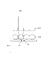
次に、図10を用いて照明光学系の例を説明する。図10は照明光学系500の概略断面図である。照明光学系500は、光源部501、コンデンサレンズ502、インテグレータ光学系503、コンデンサレンズ504を有する。光源部501から出た光束は、集光レンズ501とコンデンサレンズ502を通過して、インテグレータ光学系503に至る。集光レンズ501は、光源装置10のLEDチップの位置に対応して設けられた各レンズを有するレンズアレイである。
<Implementation of lighting equipment>
Next, an example of the illumination optical system will be described with reference to FIG. FIG. 10 is a schematic cross-sectional view of the illumination
コンデンサレンズ502は、光源部501の射出面位置とインテグレータ光学系503の入射面位置が、光学的にフーリエ共役面になるように設計されている。このような照明系をケーラー照明と呼ぶ。コンデンサレンズ502は、図10では平凸レンズ1枚を描いているが、実際は複数のレンズ群で構成されることが多い。インテグレータ光学系503を用いることにより、インテグレータ光学系503の射出面位置には、光源部501の射出面と共役な複数の二次光源像が形成される。インテグレータ光学系503の射出面から射出された光は、コンデンサレンズ504を介して照明面505に至る。
The
図11を用いて光源部501を説明する。図11は、光源部501の概略図である。光源部501は、光源装置10、集光レンズ506、集光レンズ507を有する。図11では光源装置10の一部として、LEDチップ11、電気基板12を図示している。集光レンズ506、507は、各LEDチップ11に対応して設けられた各レンズを有するレンズアレイである。集光レンズ506の各レンズは各LEDチップ11上に設けられている。レンズは、図11のような平凸レンズであっても良いし、その他のパワーがついた形状をとっても良い。レンズアレイとしては、エッチングや切削等で連続的にレンズを形成したレンズアレイや、個々のレンズを接合したレンズアレイを用いることができる。LEDチップ3から出た光は、半角で50°~70°程度の広がりを持っているが、集光レンズ506、507によって、それらは30°以下程度に変換される。集光レンズ506はLEDチップから所定の間隔だけ離されて設けられ、電気基板12とともに一体的に固定されていてもよい。
The
図10の説明に戻る。インテグレータ光学系503は、光強度分布を均一化させる機能を有する。インテグレータ光学系503には、オプティカルインテグレータレンズやロッドレンズが用いられ、照射面505の照度均一度を改善する。
Returning to the description of FIG. The integrator
コンデンサレンズ504は、インテグレータ光学系503の射出面と照明面505が光学的にフーリエ共役面になるように設計されており、インテグレータ光学系503の射出面またはその共役面は照明光学系の瞳面となる。その結果、照明面505において、ほぼ均一な光強度分布を作成することができる。
The
上記の照明光学系500は各種照明装置に適用でき、光硬化性樹脂を照明する装置、被検物を照明して検査する装置、リソグラフィ装置などにも用いることができる。例えば、マスクのパターンを基板に露光する露光装置、マスクレス露光装置、型を用いて基板にパターンを形成するインプリント装置、又は、平坦層形成装置に適用することできる。
The above-mentioned illumination
<露光装置の実施形態>
本実施形態では、上記の光源装置10や照明光学系500を露光装置に適用した場合について説明する。図12は、露光装置100の構成を示す概略図である。露光装置100は、半導体素子や液晶表示素子の製造工程であるリソグラフィ工程に採用され、基板上にパターンを形成するリソグラフィ装置である。露光装置100は、マスクを介して基板を露光して、マスクのパターンを基板に転写する。露光装置100は、本実施形態では、ステップ・アンド・スキャン方式の露光装置、所謂、走査型露光装置であるが、ステップ・アンド・リピート方式やその他の露光方式を採用しても良い。
<Embodiment of exposure apparatus>
In this embodiment, a case where the
露光装置100は、マスク101を照明する照明光学系500、マスク101のパターンを基板102上に投影する投影光学系103を有する。投影光学系103はレンズからなる投影レンズや、ミラーを用いた反射型投影系でもよい。
The
照明光学系500は、光源装置10からの光をマスク101に照明する。マスク101には、基板102に形成すべきパターンに対応するパターンが形成されている。マスク101は、マスクステージ104に保持されており、基板102は、基板ステージ105に保持されている。
The illumination
マスク101と基板102とは、投影光学系103を介して、光学的にほぼ共役な位置に配置されている。投影光学系103は、物体を像面に投影する光学系である。投影光学系103には、反射系、屈折系、反射屈折系を適用することができる。投影光学系103は、本実施形態では、所定の投影倍率を有し、マスク101に形成されたパターンを基板102に投影する。そして、マスクステージ104及び基板ステージ105を、投影光学系103の物体面と平行な方向に、投影光学系103の投影倍率に応じた速度比で走査する。これにより、マスク101に形成されたパターンを基板102に転写することができる。
The
<照射装置の実施形態>
本実施形態では、上記の光源装置10や照明光学系500を照射装置300に適用した場合について説明する。図13は、照射装置300の構成を示す概略図である。照射装置300は、被照射物301に紫外線の波長領域である照射光302を照射する紫外線照射装置として機能する。照射装置300は、光源装置10、照射制御装置303、制御部304を有する。
<Irradiation device embodiment>
In this embodiment, a case where the
被照射物301は、紫外線の照射を受けるものであれば、特に限定はされない。固体、液体、気体やその組み合わせであっても良い。照射光302は、被照射物301に何らかの作用を与える波長特性を有する紫外線である。照射光302の作用としては、殺菌処理、表面処理等が考えられる。
The
照射制御装置303は、光源装置10を制御する制御部304と接続され、制御部304との通信を行う。照射制御装置303から制御部304へと電流出力のオンオフ信号、出力電流の指令値等を出力し、制御部304を制御する。また、制御部304がLEDチップの故障を検出した場合、制御部304から照射制御装置303に故障検知信号が出力される。
The
<物品の処理の実施形態>
本発明の実施形態にかかる物品の製造方法は、例えば、FPDを製造するのに好適である。本実施形態の物品の製造方法は、基板上に塗布された感光剤に上記の露光装置を用いて潜像パターンを形成する工程(基板を露光する工程)と、かかる工程で潜像パターンが形成された基板を現像する工程とを含む。更に、かかる製造方法は、他の周知の工程(酸化、成膜、蒸着、ドーピング、平坦化、エッチング、レジスト剥離、ダイシング、ボンディング、パッケージング等)を含む。本実施形態の物品の製造方法は、従来の方法に比べて、物品の性能・品質・生産性・生産コストの少なくとも1つにおいて有利である。
<Embodiment of article processing>
The method for producing an article according to an embodiment of the present invention is suitable for producing, for example, an FPD. The method for manufacturing an article of the present embodiment includes a step of forming a latent image pattern on a photosensitive agent applied on a substrate (a step of exposing a substrate) using the above-mentioned exposure apparatus, and a step of forming a latent image pattern in such a step. It includes a step of developing the processed substrate. Further, such a manufacturing method includes other well-known steps (oxidation, film formation, vapor deposition, doping, flattening, etching, resist peeling, dicing, bonding, packaging, etc.). The method for manufacturing an article of the present embodiment is advantageous in at least one of the performance, quality, productivity, and production cost of the article as compared with the conventional method.
以上、本発明の好ましい実施形態について説明したが、本発明はこれらの実施形態に限定されないことはいうまでもなく、その要旨の範囲内で種々の変形及び変更が可能である。 Although the preferred embodiments of the present invention have been described above, it goes without saying that the present invention is not limited to these embodiments, and various modifications and changes can be made within the scope of the gist thereof.
10 光源装置
11 LEDチップ
12 電気基板
15 ヒートシンク
17 切り替え手段
18 流路
10
Claims (22)
前記電気基板に配列されている固体発光素子と、
前記電気基板に接触して配置され、内部に形成された流路を冷媒が流れるヒートシンクと、
前記流路において冷媒が流れる方向を反対の方向に切り替える切り替え手段と、
を有することを特徴とする光源装置。 With an electric board
The solid-state light emitting elements arranged on the electric substrate and
A heat sink, which is arranged in contact with the electric board and allows the refrigerant to flow through a flow path formed inside,
A switching means for switching the direction in which the refrigerant flows in the flow path in the opposite direction,
A light source device characterized by having.
前記冷媒は、前記流路と前記冷凍機を循環することを特徴とする請求項1に記載の光源装置。 Further having a refrigerator for cooling the refrigerant discharged from the flow path,
The light source device according to claim 1, wherein the refrigerant circulates between the flow path and the refrigerator.
前記第1のバルブ及び第2のバルブを含む複数のバルブと、前記第3のバルブ及び第4のバルブを含む複数のバルブとを制御することで、前記流路において冷媒が流れる方向を反対の方向に切り替えることを特徴とする請求項1乃至3のいずれか1項に記載の光源装置。 The switching means has a plurality of valves including a first valve and a second valve for controlling the refrigerant flowing through the pipe connected to one end of the heat sink, and the refrigerant flowing through the pipe connected to the other end of the heat sink. It has a third valve to control and a plurality of valves including a fourth valve.
By controlling the plurality of valves including the first valve and the second valve and the plurality of valves including the third valve and the fourth valve, the directions in which the refrigerant flows in the flow path are opposite to each other. The light source device according to any one of claims 1 to 3, wherein the light source device is switched in a direction.
前記第2のバルブは、前記冷凍機の冷媒出口に接続される配管と前記流路の冷媒出口に接続される配管とを繋いでいるバルブであり、
前記第3のバルブは、前記冷凍機の冷媒入口に接続される配管と前記流路の冷媒入口に接続される配管とを繋いでいるバルブであり、
前記第4のバルブは、前記冷凍機の冷媒入口に接続される配管と前記流路の冷媒出口に接続される配管とを繋いでいるバルブであり、
前記第1のバルブと前記第4のバルブが開いており、前記第2のバルブと前記第3のバルブが閉じている状態から、前記第1のバルブと前記第4のバルブが閉じており、前記第2のバルブと前記第3のバルブが開いている状態に切り替えることで、前記流路において冷媒が流れる方向を反対の方向に切り替えることを特徴とする請求項4に記載の光源装置。 The first valve is a valve connecting a pipe connected to the refrigerant outlet of the refrigerator and a pipe connected to the refrigerant inlet of the flow path.
The second valve is a valve connecting a pipe connected to the refrigerant outlet of the refrigerator and a pipe connected to the refrigerant outlet of the flow path.
The third valve is a valve connecting a pipe connected to the refrigerant inlet of the refrigerator and a pipe connected to the refrigerant inlet of the flow path.
The fourth valve is a valve connecting a pipe connected to the refrigerant inlet of the refrigerator and a pipe connected to the refrigerant outlet of the flow path.
The first valve and the fourth valve are closed from the state where the first valve and the fourth valve are open and the second valve and the third valve are closed. The light source device according to claim 4, wherein the direction in which the refrigerant flows in the flow path is switched in the opposite direction by switching the second valve and the third valve in an open state.
前記切り替え手段は、前記点灯時間に基づいて、前記流路において冷媒が流れる方向を反対の方向に切り替えるタイミングを決定することを特徴とする請求項1乃至6のいずれか1項に記載の光源装置。 It has a storage unit that records the lighting time of the solid-state light emitting element, and has a storage unit.
The light source device according to any one of claims 1 to 6, wherein the switching means determines a timing for switching the direction in which the refrigerant flows in the flow path in the opposite direction based on the lighting time. ..
前記切り替え手段は、前記温度センサで計測された温度及び前記点灯時間に基づいて、前記流路において冷媒が流れる方向を反対の方向に切り替えるタイミングを決定することを特徴とする請求項7に記載の光源装置。 It has a temperature sensor that records at least one of the temperature of the solid-state light emitting element and the temperature of the refrigerant flowing through the flow path.
7. The switching means according to claim 7, wherein the switching means determines a timing for switching the direction in which the refrigerant flows in the flow path in the opposite direction based on the temperature measured by the temperature sensor and the lighting time. Light source device.
前記光源に接触して配置されたヒートシンクの内部に形成された流路に冷媒を第1方向に流す第1冷却工程と、
前記冷媒が流れる方向を、前記第1方向とは反対の方向である第2方向に切り替える制御工程と、
前記流路に冷媒を前記第2方向に流す第2冷却工程と、
を含む冷却方法。 It is a cooling method that cools the light source.
A first cooling step in which the refrigerant flows in the first direction through a flow path formed inside the heat sink arranged in contact with the light source.
A control step of switching the direction in which the refrigerant flows to a second direction opposite to the first direction,
A second cooling step in which the refrigerant flows through the flow path in the second direction,
Cooling method including.
前記冷媒は、前記流路と前記冷凍機とを循環することを特徴とする請求項10又は11に記載の冷却方法。 In the first cooling step and the second cooling step, the refrigerant discharged from the flow path is cooled by a refrigerator.
The cooling method according to claim 10 or 11, wherein the refrigerant circulates between the flow path and the refrigerator.
前記制御工程は、前記冷凍機の冷媒出口と前記流路の他端が配管で接続され、前記冷凍機の冷媒入口と前記流路の一端が配管で接続されるように配管の接続先を入れ替えることで、前記冷媒が流れる方向を切り替えることを特徴とする請求項10乃至12のいずれか1項に記載の冷却方法。 In the first cooling step, the refrigerant outlet of the refrigerator and one end of the flow path are connected by a pipe, and the refrigerant inlet of the refrigerator and the other end of the flow path are connected by a pipe.
In the control step, the connection destinations of the pipes are exchanged so that the refrigerant outlet of the refrigerator and the other end of the flow path are connected by a pipe, and the refrigerant inlet of the refrigerator and one end of the flow path are connected by a pipe. The cooling method according to any one of claims 10 to 12, wherein the direction in which the refrigerant flows is switched.
前記記憶工程により記憶された前記光源の点灯時間に基づいて、前記制御工程が行われるタイミングを決定することを特徴とする請求項10乃至14のいずれか1項に記載の冷却方法。 Further including a storage step of storing the time when the light source is lit,
The cooling method according to any one of claims 10 to 14, wherein the timing at which the control step is performed is determined based on the lighting time of the light source stored by the storage step.
前記計測工程により計測された前記光源及び前記冷媒の少なくとも一方の温度と、前記記憶工程により記憶された前記光源の点灯時間とに基づいて、前記制御工程が行われるタイミングを決定することを特徴とする請求項15に記載の冷却方法。 Prior to the control step, a measurement step of measuring the temperature of at least one of the light source and the refrigerant is further included.
It is characterized in that the timing at which the control step is performed is determined based on the temperature of at least one of the light source and the refrigerant measured by the measurement step and the lighting time of the light source stored by the storage step. The cooling method according to claim 15.
コンデンサレンズと、
オプティカルインテグレータを有し、
複数の前記固体発光素子のそれぞれからの光強度分布を、前記コンデンサレンズを介して、前記オプティカルインテグレータの入射面において重ね合わせることを特徴とする照明装置。 The light source device according to any one of claims 1 to 9.
With a condenser lens
Has an optical integrator and
A lighting device comprising superimposing light intensity distributions from each of a plurality of solid-state light emitting elements on an incident surface of the optical integrator via the condenser lens.
前記マスクのパターンを基板に露光する露光手段を有することを特徴とする露光装置。 An illuminating optical system that illuminates a mask with light from the illuminating device according to claim 17 or 18.
An exposure apparatus comprising an exposure means for exposing the mask pattern to a substrate.
前記光源を冷却するために前記光源に接触して配置されたヒートシンクの内部の流路において、第1方向に冷媒を流しながら前記照明光によりマスクのパターンを基板に露光する工程と、
前記光源が消灯しているタイミングで、前記流路を流れる冷媒の方向を前記第1方向とは反対方向の第2方向に切り替える工程と、
前記流路において、前記第2方向に冷媒を流しながら前記照明光によりマスクのパターンを基板に露光する工程と、
を含むことを特徴とする露光方法。 An exposure method in which a mask is irradiated with the illumination light emitted from the light source while cooling the light source, and the pattern of the mask is exposed on the substrate.
A step of exposing a mask pattern to a substrate by the illumination light while flowing a refrigerant in a first direction in a flow path inside a heat sink arranged in contact with the light source to cool the light source.
A step of switching the direction of the refrigerant flowing through the flow path to a second direction opposite to the first direction at the timing when the light source is turned off.
A step of exposing a mask pattern to a substrate by the illumination light while flowing a refrigerant in the second direction in the flow path.
An exposure method comprising.
前記光は、前記被照射物の殺菌処理、及び表面処理の少なくとも一方の処理を行うことを特徴とする照射装置。 An irradiation device that irradiates an object to be irradiated with light using the light source device according to any one of claims 1 to 9.
The light is an irradiation device characterized by performing at least one of a sterilization treatment and a surface treatment of the irradiated object.
前記露光工程で露光された基板を現像する現像工程と、
を含み、
前記現像工程で処理された基板から物品を製造することを特徴とする物品の製造方法。 An exposure step of exposing a substrate by using the exposure method according to claim 20.
A developing process for developing a substrate exposed in the exposure process, and a development process for developing the substrate.
Including
A method for manufacturing an article, which comprises manufacturing an article from a substrate processed in the developing step.
Priority Applications (5)
| Application Number | Priority Date | Filing Date | Title |
|---|---|---|---|
| JP2020203466A JP2022090891A (en) | 2020-12-08 | 2020-12-08 | Light source apparatus, cooling method, and method for manufacturing goods |
| TW110142869A TW202223551A (en) | 2020-12-08 | 2021-11-18 | Light source device, cooling method, and manufacturing method for product |
| KR1020210168030A KR20220081288A (en) | 2020-12-08 | 2021-11-30 | Light source device, cooling method, and manufacturing method for product |
| CN202111463603.1A CN114624962A (en) | 2020-12-08 | 2021-12-03 | Light source apparatus, cooling method and product manufacturing method |
| US17/542,195 US11815253B2 (en) | 2020-12-08 | 2021-12-03 | Light source device, cooling method, and manufacturing method for product |
Applications Claiming Priority (1)
| Application Number | Priority Date | Filing Date | Title |
|---|---|---|---|
| JP2020203466A JP2022090891A (en) | 2020-12-08 | 2020-12-08 | Light source apparatus, cooling method, and method for manufacturing goods |
Publications (2)
| Publication Number | Publication Date |
|---|---|
| JP2022090891A true JP2022090891A (en) | 2022-06-20 |
| JP2022090891A5 JP2022090891A5 (en) | 2023-11-17 |
Family
ID=81847891
Family Applications (1)
| Application Number | Title | Priority Date | Filing Date |
|---|---|---|---|
| JP2020203466A Pending JP2022090891A (en) | 2020-12-08 | 2020-12-08 | Light source apparatus, cooling method, and method for manufacturing goods |
Country Status (5)
| Country | Link |
|---|---|
| US (1) | US11815253B2 (en) |
| JP (1) | JP2022090891A (en) |
| KR (1) | KR20220081288A (en) |
| CN (1) | CN114624962A (en) |
| TW (1) | TW202223551A (en) |
Cited By (1)
| Publication number | Priority date | Publication date | Assignee | Title |
|---|---|---|---|---|
| WO2024038538A1 (en) * | 2022-08-18 | 2024-02-22 | 株式会社ニコン | Light source unit, illumination unit, exposure device, and exposure method |
Families Citing this family (1)
| Publication number | Priority date | Publication date | Assignee | Title |
|---|---|---|---|---|
| JP2022090891A (en) * | 2020-12-08 | 2022-06-20 | キヤノン株式会社 | Light source apparatus, cooling method, and method for manufacturing goods |
Family Cites Families (3)
| Publication number | Priority date | Publication date | Assignee | Title |
|---|---|---|---|---|
| JP2011165509A (en) | 2010-02-10 | 2011-08-25 | Moritex Corp | Led lighting system |
| EP3301999B1 (en) * | 2016-09-30 | 2020-06-17 | HP Scitex Ltd | Light emitting diode heatsink |
| JP2022090891A (en) * | 2020-12-08 | 2022-06-20 | キヤノン株式会社 | Light source apparatus, cooling method, and method for manufacturing goods |
-
2020
- 2020-12-08 JP JP2020203466A patent/JP2022090891A/en active Pending
-
2021
- 2021-11-18 TW TW110142869A patent/TW202223551A/en unknown
- 2021-11-30 KR KR1020210168030A patent/KR20220081288A/en active Search and Examination
- 2021-12-03 CN CN202111463603.1A patent/CN114624962A/en active Pending
- 2021-12-03 US US17/542,195 patent/US11815253B2/en active Active
Cited By (1)
| Publication number | Priority date | Publication date | Assignee | Title |
|---|---|---|---|---|
| WO2024038538A1 (en) * | 2022-08-18 | 2024-02-22 | 株式会社ニコン | Light source unit, illumination unit, exposure device, and exposure method |
Also Published As
| Publication number | Publication date |
|---|---|
| KR20220081288A (en) | 2022-06-15 |
| CN114624962A (en) | 2022-06-14 |
| US20220178533A1 (en) | 2022-06-09 |
| TW202223551A (en) | 2022-06-16 |
| US11815253B2 (en) | 2023-11-14 |
Similar Documents
| Publication | Publication Date | Title |
|---|---|---|
| CN100377303C (en) | Reflection mirror apparatus, exposure apparatus and device manufacturing method | |
| US7250616B2 (en) | Temperature adjustment apparatus, exposure apparatus having the same, and device fabricating method | |
| WO2006004135A1 (en) | Exposure apparatus and device manufacturing method | |
| US11815253B2 (en) | Light source device, cooling method, and manufacturing method for product | |
| US7692766B2 (en) | Lithographic apparatus | |
| US20100231879A1 (en) | Exposure apparatus, exposure method, and device manufacturing method | |
| JP5214771B2 (en) | Lithographic apparatus and lithographic apparatus cooling method | |
| JP2007317847A (en) | Aligner, and manufacturing method of device | |
| US7295285B2 (en) | Exposure apparatus and device manufacturing method | |
| JP2004247438A (en) | Cooling apparatus | |
| US7106413B2 (en) | Cooling mechanism | |
| US9063406B2 (en) | Exposure apparatus and a method of manufacturing a device that conduct exposure using a set light source shape | |
| US7319505B2 (en) | Exposure apparatus and device fabrication method | |
| JP2004080025A (en) | Cooling device and method therefor, and aligner therewith | |
| JP7418128B2 (en) | Light source device, illumination device, and exposure device. | |
| KR101761279B1 (en) | LED array light source module for exposing large area pattern and apparatus for controlling the LED array light source module | |
| JP7458853B2 (en) | Light source device, illumination device, and exposure device. | |
| TW202217188A (en) | Light source device, lighting device, exposure device, irradiation device, and method for manufacturing article to reduce the uneven distribution of light emitted from a plurality of LED chips | |
| JP2023073019A (en) | Light source device, exposure device, and article manufacturing method | |
| JP2013187505A (en) | Illumination device, illumination system, exposure device, exposure method, and device manufacturing method | |
| JP2023015808A (en) | Light source apparatus, exposure apparatus, and method for manufacturing article | |
| JP2004247473A (en) | Cooling device and method, and aligner including the same | |
| JP2021193407A (en) | Light source device, exposure device and manufacturing method of articles | |
| JP2001023890A (en) | Aligner and manufacture of device using the same | |
| JP2005243771A (en) | Aligner |
Legal Events
| Date | Code | Title | Description |
|---|---|---|---|
| RD01 | Notification of change of attorney |
Free format text: JAPANESE INTERMEDIATE CODE: A7421 Effective date: 20210108 |
|
| A521 | Request for written amendment filed |
Free format text: JAPANESE INTERMEDIATE CODE: A523 Effective date: 20231108 |
|
| A621 | Written request for application examination |
Free format text: JAPANESE INTERMEDIATE CODE: A621 Effective date: 20231108 |
|
| RD01 | Notification of change of attorney |
Free format text: JAPANESE INTERMEDIATE CODE: A7421 Effective date: 20231213 |