JP2023015808A - Light source apparatus, exposure apparatus, and method for manufacturing article - Google Patents
Light source apparatus, exposure apparatus, and method for manufacturing article Download PDFInfo
- Publication number
- JP2023015808A JP2023015808A JP2021119815A JP2021119815A JP2023015808A JP 2023015808 A JP2023015808 A JP 2023015808A JP 2021119815 A JP2021119815 A JP 2021119815A JP 2021119815 A JP2021119815 A JP 2021119815A JP 2023015808 A JP2023015808 A JP 2023015808A
- Authority
- JP
- Japan
- Prior art keywords
- leds
- current
- light
- light emission
- emission amount
- Prior art date
- Legal status (The legal status is an assumption and is not a legal conclusion. Google has not performed a legal analysis and makes no representation as to the accuracy of the status listed.)
- Pending
Links
- 238000000034 method Methods 0.000 title claims description 26
- 238000004519 manufacturing process Methods 0.000 title claims description 14
- 239000002826 coolant Substances 0.000 claims abstract description 39
- 239000000758 substrate Substances 0.000 claims description 29
- 238000003491 array Methods 0.000 claims description 18
- 230000005484 gravity Effects 0.000 claims description 8
- 230000001186 cumulative effect Effects 0.000 claims description 4
- 239000000463 material Substances 0.000 claims description 4
- 238000005192 partition Methods 0.000 claims description 4
- 230000003287 optical effect Effects 0.000 description 23
- 238000010586 diagram Methods 0.000 description 15
- 238000001816 cooling Methods 0.000 description 7
- 238000011144 upstream manufacturing Methods 0.000 description 7
- 238000005286 illumination Methods 0.000 description 5
- QSHDDOUJBYECFT-UHFFFAOYSA-N mercury Chemical compound [Hg] QSHDDOUJBYECFT-UHFFFAOYSA-N 0.000 description 5
- 229910052753 mercury Inorganic materials 0.000 description 5
- 230000007423 decrease Effects 0.000 description 3
- 238000011161 development Methods 0.000 description 3
- 239000007788 liquid Substances 0.000 description 3
- 239000004065 semiconductor Substances 0.000 description 3
- CJVFIJXEPCVCTK-LWMBYGOMSA-N (2s)-2-[[2-[[(2s)-2-[[(2s)-2-[[(2s)-2-[[(2s)-2-[[(2s)-2-[[(2s)-2-amino-3-methylbutanoyl]amino]propanoyl]amino]-3-methylbutanoyl]amino]-4-methylpentanoyl]amino]-3-methylbutanoyl]amino]-4-methylpentanoyl]amino]acetyl]amino]propanoic acid Chemical compound OC(=O)[C@H](C)NC(=O)CNC(=O)[C@H](CC(C)C)NC(=O)[C@H](C(C)C)NC(=O)[C@H](CC(C)C)NC(=O)[C@@H](NC(=O)[C@H](C)NC(=O)[C@@H](N)C(C)C)C(C)C CJVFIJXEPCVCTK-LWMBYGOMSA-N 0.000 description 2
- 238000007664 blowing Methods 0.000 description 2
- 239000002131 composite material Substances 0.000 description 2
- 230000003247 decreasing effect Effects 0.000 description 2
- 230000001419 dependent effect Effects 0.000 description 2
- 230000008021 deposition Effects 0.000 description 2
- 238000001459 lithography Methods 0.000 description 2
- 239000011159 matrix material Substances 0.000 description 2
- 238000012546 transfer Methods 0.000 description 2
- RYGMFSIKBFXOCR-UHFFFAOYSA-N Copper Chemical compound [Cu] RYGMFSIKBFXOCR-UHFFFAOYSA-N 0.000 description 1
- 230000002411 adverse Effects 0.000 description 1
- 230000004075 alteration Effects 0.000 description 1
- 229910052782 aluminium Inorganic materials 0.000 description 1
- XAGFODPZIPBFFR-UHFFFAOYSA-N aluminium Chemical compound [Al] XAGFODPZIPBFFR-UHFFFAOYSA-N 0.000 description 1
- 230000015572 biosynthetic process Effects 0.000 description 1
- 239000003795 chemical substances by application Substances 0.000 description 1
- 238000007796 conventional method Methods 0.000 description 1
- 229910052802 copper Inorganic materials 0.000 description 1
- 239000010949 copper Substances 0.000 description 1
- 238000012937 correction Methods 0.000 description 1
- 230000000694 effects Effects 0.000 description 1
- 238000005530 etching Methods 0.000 description 1
- 239000011521 glass Substances 0.000 description 1
- 239000004519 grease Substances 0.000 description 1
- AMGQUBHHOARCQH-UHFFFAOYSA-N indium;oxotin Chemical compound [In].[Sn]=O AMGQUBHHOARCQH-UHFFFAOYSA-N 0.000 description 1
- 239000004973 liquid crystal related substance Substances 0.000 description 1
- 238000012986 modification Methods 0.000 description 1
- 230000004048 modification Effects 0.000 description 1
- 230000003647 oxidation Effects 0.000 description 1
- 238000007254 oxidation reaction Methods 0.000 description 1
- 238000004806 packaging method and process Methods 0.000 description 1
- 239000003507 refrigerant Substances 0.000 description 1
- 230000035945 sensitivity Effects 0.000 description 1
- 238000003786 synthesis reaction Methods 0.000 description 1
- 230000002194 synthesizing effect Effects 0.000 description 1
- XLYOFNOQVPJJNP-UHFFFAOYSA-N water Substances O XLYOFNOQVPJJNP-UHFFFAOYSA-N 0.000 description 1
Images


Classifications
-
- G—PHYSICS
- G03—PHOTOGRAPHY; CINEMATOGRAPHY; ANALOGOUS TECHNIQUES USING WAVES OTHER THAN OPTICAL WAVES; ELECTROGRAPHY; HOLOGRAPHY
- G03F—PHOTOMECHANICAL PRODUCTION OF TEXTURED OR PATTERNED SURFACES, e.g. FOR PRINTING, FOR PROCESSING OF SEMICONDUCTOR DEVICES; MATERIALS THEREFOR; ORIGINALS THEREFOR; APPARATUS SPECIALLY ADAPTED THEREFOR
- G03F7/00—Photomechanical, e.g. photolithographic, production of textured or patterned surfaces, e.g. printing surfaces; Materials therefor, e.g. comprising photoresists; Apparatus specially adapted therefor
- G03F7/70—Microphotolithographic exposure; Apparatus therefor
- G03F7/70483—Information management; Active and passive control; Testing; Wafer monitoring, e.g. pattern monitoring
- G03F7/7055—Exposure light control in all parts of the microlithographic apparatus, e.g. pulse length control or light interruption
-
- G—PHYSICS
- G03—PHOTOGRAPHY; CINEMATOGRAPHY; ANALOGOUS TECHNIQUES USING WAVES OTHER THAN OPTICAL WAVES; ELECTROGRAPHY; HOLOGRAPHY
- G03F—PHOTOMECHANICAL PRODUCTION OF TEXTURED OR PATTERNED SURFACES, e.g. FOR PRINTING, FOR PROCESSING OF SEMICONDUCTOR DEVICES; MATERIALS THEREFOR; ORIGINALS THEREFOR; APPARATUS SPECIALLY ADAPTED THEREFOR
- G03F7/00—Photomechanical, e.g. photolithographic, production of textured or patterned surfaces, e.g. printing surfaces; Materials therefor, e.g. comprising photoresists; Apparatus specially adapted therefor
- G03F7/70—Microphotolithographic exposure; Apparatus therefor
- G03F7/70008—Production of exposure light, i.e. light sources
- G03F7/7005—Production of exposure light, i.e. light sources by multiple sources, e.g. light-emitting diodes [LED] or light source arrays
-
- G—PHYSICS
- G03—PHOTOGRAPHY; CINEMATOGRAPHY; ANALOGOUS TECHNIQUES USING WAVES OTHER THAN OPTICAL WAVES; ELECTROGRAPHY; HOLOGRAPHY
- G03F—PHOTOMECHANICAL PRODUCTION OF TEXTURED OR PATTERNED SURFACES, e.g. FOR PRINTING, FOR PROCESSING OF SEMICONDUCTOR DEVICES; MATERIALS THEREFOR; ORIGINALS THEREFOR; APPARATUS SPECIALLY ADAPTED THEREFOR
- G03F7/00—Photomechanical, e.g. photolithographic, production of textured or patterned surfaces, e.g. printing surfaces; Materials therefor, e.g. comprising photoresists; Apparatus specially adapted therefor
- G03F7/70—Microphotolithographic exposure; Apparatus therefor
- G03F7/708—Construction of apparatus, e.g. environment aspects, hygiene aspects or materials
- G03F7/70858—Environment aspects, e.g. pressure of beam-path gas, temperature
- G03F7/70883—Environment aspects, e.g. pressure of beam-path gas, temperature of optical system
- G03F7/70891—Temperature
Abstract
Description
本発明は、光源装置、露光装置、及び物品の製造方法に関する。 The present invention relates to a light source device, an exposure device, and an article manufacturing method.
露光装置は、半導体デバイスや液晶表示装置等の製造工程であるリソグラフィ工程において、原版(レチクル又はマスク)のパターンを、投影光学系を介して感光性の基板(表面にレジスト層が形成されたウエハやガラスプレート等)に転写する装置である。このパターン転写用の光源(露光光源)としては、例えば、水銀ランプが用いられているが、近年では、発光ダイオード(LED:Light Emitting Diode)へ置き換えられることが期待されている。LEDは、発光を制御する回路に電流を流してから光の出力が安定するまでの時間が短く、水銀ランプのように常時発光させる必要がないため、長寿命でもある。ただし、LED1個当たりの輝度は小さいため、水銀ランプの代わりにLEDを光源に用いるためには、複数のLEDを集積させて露光光源として発光する光の発光量を向上させる必要がある。 An exposure apparatus projects a pattern of an original (reticle or mask) onto a photosensitive substrate (wafer with a resist layer formed on its surface) via a projection optical system in the lithography process, which is the manufacturing process for semiconductor devices, liquid crystal display devices, and the like. , glass plate, etc.). As a light source (exposure light source) for this pattern transfer, for example, a mercury lamp is used, but in recent years, it is expected to be replaced by a light emitting diode (LED). The LED has a long lifespan because it takes a short time for the light output to stabilize after a current is applied to the circuit that controls light emission, and unlike a mercury lamp, it does not need to emit light all the time. However, since the brightness of each LED is small, in order to use an LED as a light source instead of a mercury lamp, it is necessary to integrate a plurality of LEDs to increase the amount of light emitted as an exposure light source.
露光装置の生産性を向上させるためには、露光光源の発光量を大きくする必要があるが、集積させた各LEDに流れる電流値を大きくして発光量を大きくするとLEDの発熱量も大きくなってしまう。また露光装置は、露光対象によって、パターン転写に大光量を必要とせず、LEDに流れる電流値を小さくして発光量を小さくする場合もある。 In order to improve the productivity of the exposure apparatus, it is necessary to increase the amount of light emitted from the exposure light source. However, increasing the amount of light emitted by increasing the current flowing through each integrated LED increases the amount of heat generated by the LEDs. end up Depending on the exposure target, the exposure apparatus may reduce the amount of light emission by reducing the current value flowing through the LED without requiring a large amount of light for pattern transfer.
上記のように露光対象に応じてLEDに流れる電流値を変更すると、LEDで発生する熱量が変化するため、LEDの温度が変化する。LEDは、LEDの温度に応じて、LEDから出射される光のピーク波長が変動する温度依存特性を有する。また、露光装置は、露光光源からの光の波長(露光光の波長)の変動により露光性能が低下してしまうおそれがあるため、露光光源にLEDを用いる場合も露光光のピーク波長の変動は好ましくない。例えば、LEDは15℃程度の温度変化で2nm程度の波長変動が発生し、露光処理に悪影響を及ぼすおそれがあるからである。 When the value of the current flowing through the LED is changed according to the exposure target as described above, the amount of heat generated by the LED changes, so the temperature of the LED changes. An LED has a temperature dependent characteristic in which the peak wavelength of light emitted from the LED varies according to the temperature of the LED. In addition, the exposure performance of the exposure apparatus may deteriorate due to fluctuations in the wavelength of the light emitted from the exposure light source (the wavelength of the exposure light). I don't like it. For example, a temperature change of about 15° C. causes a wavelength variation of about 2 nm in an LED, which may adversely affect the exposure process.
特許文献1には、LEDモジュールから光のピーク波長の変動を抑制するための手法が記載されている。具体的には、LEDグループ別に波長特性が異なるLEDモジュールから発光させるLEDグループを選択し、選択したLEDグループのLEDの温度に基づいてLEDに流す電流値を補正することにより、光のピーク波長の変動を抑制している。
しかしながら特許文献1は、LEDモジュールの発光量を可変とする事は記載しておらず、発光量の変更により生じるLEDモジュールからの光のピーク波長の変動を抑制する手法は示していない。
However,
そこで、本発明は、発光量の変更により生じるLEDモジュールからの光のピーク波長の変動を抑制する上で有利な光源装置を提供することを目的とする。 SUMMARY OF THE INVENTION Accordingly, it is an object of the present invention to provide a light source device that is advantageous in suppressing variations in the peak wavelength of light emitted from an LED module caused by changes in the amount of light emitted.
上記目的を達成するために、本発明の一側面としての光源装置は、複数のLEDが配列されているLEDモジュールと、内部を流れる冷媒により前記LEDモジュールを冷却する冷却器とを有し、前記LEDモジュールの発光量が可変な光源装置であって、前記発光量が第1の発光量の場合に所定の電流値より大きな電流を流して発光させるLEDの数が、前記発光量が前記第1の発光量より大きな第2の発光量の場合に前記所定の電流値より大きな電流を流して発光させるLEDの数より少ないことを特徴とする。 In order to achieve the above object, a light source device as one aspect of the present invention includes an LED module in which a plurality of LEDs are arranged, and a cooler for cooling the LED module with a coolant flowing therein, In the light source device in which the light emission amount of the LED module is variable, when the light emission amount is the first light emission amount, the number of LEDs to emit light by flowing a current larger than a predetermined current value is set so that the light emission amount is the first light emission amount. is smaller than the number of LEDs which are caused to emit light by flowing a current larger than the predetermined current value in the case of the second light emission quantity larger than the light emission quantity of .
本発明によれば、発光量の変更により生じるピーク波長の変動を抑制する上で有利な光源装置を提供することができる。 According to the present invention, it is possible to provide a light source device that is advantageous in suppressing fluctuations in peak wavelength caused by changes in the amount of light emitted.
以下に、本発明の好ましい実施形態を添付の図面に基づいて詳細に説明する。尚、各図において、同一の部材については同一の参照番号を付し、重複する説明は省略する。 Preferred embodiments of the present invention are described in detail below with reference to the accompanying drawings. In addition, in each figure, the same reference numerals are given to the same members, and redundant explanations are omitted.
<第1実施形態>
本実施形態における光源装置について説明する。図1は、光源装置10の構成を示す概略図である。光源装置10は、回路基板11に複数のLED1(LEDチップ)が配列されているチップ列2が複数個備えられているLEDモジュール3と、電源4と、温度調節器5と、冷却器と、制御部7とを有する。以下の説明では、1つのLEDの素子を指し示す用語として、LEDチップという用語を用いる。冷却器は、図1では不図示であるが、LEDモジュール3のLEDチップ1が配置されている基板11表面とは反対側の基板11裏面に接触して設けられている。本実施形態におけるLEDモジュール3の発光量は、可変である。
<First Embodiment>
A light source device according to this embodiment will be described. FIG. 1 is a schematic diagram showing the configuration of the
回路基板11には、配線14がLEDチップ1に接続・実装されており、LEDチップ1を発光させるための回路が形成されている。チップ列2は、複数のLEDチップ1が直列に接続されている。回路に電流を流すことで、LEDチップ1から所定の波長の光が出力され、LEDチップ1が発熱する。そのような構成のLEDモジュール3のパッケージタイプは、一般的に、Chip On Board(以下ではCOBと呼ぶ)とも称される。COBは、多くのLEDチップを集積できるため、大きな光量を得ることができる点で有利である。図1に示す例では、LEDモジュール3は、6個のチップ列を備えており、それぞれのチップ列2は10個のLEDチップ1を有している。LEDチップ1は、チップ列毎に電源4から配線14を通して電流が供給されることにより光を出射する。
A
制御部7は、LEDモジュール3の発光量を取得する取得部8と、LEDモジュール3のそれぞれのチップ列2に流れる電流を制御する電流制御部9(光量変更部)とを有する。取得部8は、取得した発光量を電流制御部9に伝達する。取得部8は、例えば、外部装置からLEDモジュールに求められる発光量に関する情報を受信する。取得部8は、これに限らず、ユーザによって求められる発光量が入力されることにより発光量に関する情報を取得しても良い。電流制御部9は、取得部8で取得した発光量に基づいて、それぞれのチップ列2に流す電流値を決定し、電源4を駆動する。電源4は、回路基板11上の1つ1つのLEDチップが個別に点灯するように駆動することはできないが、チップ列単位で点灯するように駆動することができる。
The
温度調節器5は、配管6を通して、一定温度に制御された冷媒を冷却器に供給する。冷却器の内部を冷媒が一定の速度で流れることで、LEDチップ1が点灯する際に発生する熱を冷却する。熱を奪った後の冷媒は、温度調節器5へと循環し、温度調節器5で冷却されることで再びLEDチップ1の熱を冷却することができる。
A
LEDチップ1に大きな電流を流した場合、LEDチップ1からの発熱量も大きくなり、温度が上昇する。LEDチップ1は半導体を用いているため、所定の温度を超えた場合に壊れてしまうおそれがある。白熱電球と対比した場合、白熱電球は発光時に100℃以上になるが、LEDチップ1は100℃を超える温度では動作しない。そこで、温度の上昇を抑制するための冷却器を光源装置10に備える必要がある。また、LEDには、温度が低いほど発光効率が高くなるという特性があるため、冷却器を光源装置10に備えることが望ましい。
When a large current flows through the
冷却器による冷却効率を向上させるために、熱伝導率が高い素材を回路基板11に用いることが好ましい。回路基板11の材質としては、例えば、熱伝導率が高い銅やアルミニウムを含む材料を用いると良い。冷媒には、例えば、冷却力が優れている水を主成分とする液体や、電気絶縁性に優れたオイルを主成分する液体が用いられうる。本実施形態では、冷媒として液体を用いる例について説明するが、これに限らず、例えば、昇温時のLEDチップ1より温度の低い気体を吹き付けることによる空冷によりLEDチップ1を冷却しても良い。空冷するときは気体を吹き出すノズル等を備える冷却器を設ける。
In order to improve the cooling efficiency of the cooler, it is preferable to use a material with high thermal conductivity for the
図2は、冷却器12の構成を示す概略図である。冷却器12は、LEDモジュール3に接触して設けられているが、冷却器12とLEDモジュール3との間に熱伝導性を高めるための伝導グリスなどが塗布されていても良い。冷却器12の内部には、冷媒が流れる流路13が形成されており、LEDモジュール3のそれぞれのチップ列2におけるLEDチップ1が配列される方向と平行な方向に冷媒が流れる。尚、LEDモジュール3のそれぞれのチップ列2におけるLEDチップ1が配列される第1方向は、冷媒が流れる第2方向に対して、平行な成分を含む方向であれば良いが、第1方向が第2方向に対して45度以内の角度の方向であることが好ましい。また、第1方向が第2方向に対して平行に近いほど、後述する効果を得ることができるため、第1方向が第2方向に対して15度以内の角度の方向であることが好ましい。
FIG. 2 is a schematic diagram showing the configuration of the cooler 12. As shown in FIG. The cooler 12 is provided in contact with the
LEDチップは、LEDチップの温度に応じて、LEDチップから出射される光のピーク波長が変動する温度依存特性を有する。また、照明する対象に応じて必要な照度や露光量等が変わる場合、LEDモジュールの目標発光量が変更される。発光量を変更するために各LEDチップに流れる電流値を変更した場合に、大部分または全部のLEDチップの温度が変化し、各LEDチップから出射される光(LEDモジュールからの光)のピーク波長が変動する。 An LED chip has a temperature dependent characteristic in which the peak wavelength of light emitted from the LED chip varies according to the temperature of the LED chip. In addition, when the necessary illuminance, exposure amount, etc. change according to the object to be illuminated, the target light emission amount of the LED module is changed. When the current value flowing through each LED chip is changed in order to change the light emission amount, the temperature of most or all of the LED chips changes, and the light emitted from each LED chip (light from the LED module) peaks. Wavelength fluctuates.
図3は、発光量に応じてLEDチップ1に流す電流値を変更したときのLEDチップ1の温度を示す概念図である。図3のグラフには、3つの異なる発光量1~3でLEDチップ1を点灯させた場合のLEDチップ1の位置と温度の関係が示されている。図3のグラフの上部に示す図は、光源装置10の断面図であり、LEDチップ1の位置とグラフの横軸が対応することを示している。発光量1(第2の発光量)となるようにLEDチップ1を点灯させるためには、全てのLEDチップ1に1Aの電流を流せば良い。発光量1の50%の発光量である発光量2(第1の発光量)となるようにLEDチップ1を点灯させるためには、全てのLEDチップ1に0.5Aの電流を流せば良い。発光量1の33%の発光量である発光量3となるようにLEDチップ1を点灯させるためには、全てのLEDチップ1に0.33Aの電流を流せば良い。
FIG. 3 is a conceptual diagram showing the temperature of the
冷媒の上流側では冷媒の温度が比較的低く冷却力が大きいが、冷媒の下流側では既に冷媒への熱伝達が行われて冷媒の温度が上昇しているため冷却力が低下し、LEDチップの温度も高くなる。発光量1の場合、冷媒の上流側ではLEDチップ1の温度は20℃程度であるが、冷媒の下流側ではLEDチップ1の温度は80℃程度となる。したがって、全LEDチップ1の平均温度は50℃程度となる。発光量2の場合、冷媒の上流側ではLEDチップ1の温度は20℃程度であるが、冷媒の下流側ではLEDチップ1の温度は50℃程度となる。したがって、全LEDチップ1の平均温度は35℃程度となる。発光量3の場合、冷媒の上流側ではLEDチップ1の温度は20℃程度であるが、冷媒の下流側ではLEDチップ1の温度は32℃程度となる。したがって、全LEDチップ1の平均温度は26℃程度となる。
On the upstream side of the coolant, the temperature of the coolant is relatively low and the cooling power is large, but on the downstream side of the coolant, heat has already been transferred to the coolant and the temperature of the coolant has risen, so the cooling power is reduced and the LED chip temperature also increases. When the light emission amount is 1, the temperature of the
図3に示すように、発光量1~3を変更した場合に、LEDチップ1の温度は特に下流側で大きく変化する。光源装置10を、例えば、露光装置に適用する場合には、露光光のピーク波長の変動を2nm程度以内に抑える必要がある。露光光のピーク波長の変動を2nm程度以内に抑えるためには、全LEDチップ1の平均温度の異なる発光量間での差異(以下「許容温度差」と記す事も有る)を15℃以内程度にしなければならない。図3では、発光量1の平均温度50℃と発光量3の平均温度26℃では、平均温度の差異が24℃であるため、許容温度差15℃を超えてしまい、露光光のピーク波長の変動が2nm以上となってしまう。
As shown in FIG. 3, when the light emission amounts 1 to 3 are changed, the temperature of the
本実施形態では、LEDモジュールの発光量を変更したときのLEDモジュールから出射される光のピーク波長の変動を低減できる光源装置10に流す電流の制御方法について説明する。本実施形態の光源装置10では、発光量に基づいて、電流を流すチップ列2を選択する。すなわち、発光量に基づいて、LEDモジュール3の複数のチップ列のうち、電流を流すチップ列の数と電流を流さないチップ列の数それぞれの全チップ列の数に対する割合を決定する。
In this embodiment, a method of controlling the current flowing through the
また、例えばチップ列が形成されていないLEDモジュール3の形態、例えば個々に電流制御が可能な多数個のLEDチップをマトリクス状に配置した形態であっても良い。その場合には、電流を流すLEDチップの数と電流を流さないLEDチップの数それぞれの全LEDチップ数に対する割合を決定しても良い。
Alternatively, for example, the form of the
図4は、本実施形態におけるLEDチップ1の点灯方法を示す図である。図4(a)は発光量1(第2の発光量)の点灯方法である。図4(a)では、点線で囲んでいる6つのチップ列2の全てに(すなわち全LEDチップに)互いに同じ大きさ(電流値)の電流が流れるように電流制御部9が電源4を制御する。
FIG. 4 is a diagram showing a lighting method of the
図4(b)は発光量2(発光量1の50%の発光量、第1の発光量)の点灯方法である。6つのチップ列2のうち3つのチップ列にのみ(すなわち全LEDチップの半数のLEDチップのみ)に互いに同じ大きさの電流が流れるように電流制御部9が電源4を制御する。このとき、図4(a)で6つのチップ列に流した電流値と同じ電流値を点線で囲んでいる3つのチップ列に流す。すなわち、電流制御部9は、第1の発光量の場合に、複数のLEDチップのうち所定の電流値より大きな電流を流して発光させるLED以外のLEDチップには、電流を流さないように制御する。
FIG. 4(b) shows a lighting method of light emission amount 2 (50% light emission amount of
図4(c)は発光量3(発光量1の33%の発光量)の点灯方法である。6つのチップ列2のうち点線で囲んでいる2つのチップ列にのみ電流が流れるように電流制御部9が電源4を制御する。このとき、図4(a)で6つのチップ列に流した電流値と同じ電流値を2つのチップ列に流す。
FIG. 4C shows a lighting method with a light emission amount of 3 (33% of the light emission amount of 1). The
図5は、発光量に応じて電流を流すチップ列の数を変更したときのLEDチップ1の温度を示す概念図である。図5のグラフには、図3と同様に、3つの異なる発光量1~3でLEDチップ1を点灯させた場合のLEDチップ1の位置と温度の関係が示されている。図5のグラフの上部に示す図は、光源装置10の断面図であり、LEDチップ1の位置とグラフの横軸が対応することを示している。発光量1となるようにLEDチップ1を点灯させるためには、全てのLEDチップ1に1Aの電流を流せば良い。発光量1の50%の発光量である発光量2となるようにLEDチップ1を点灯させるためには、図4(b)のように6つのチップ列のうち3つのチップ列2に1Aの電流を流し、残りのチップ列には電流が流れないようにすれば良い。発光量1の33%の発光量である発光量3となるようにLEDチップ1を点灯させるためには、2つのチップ列2に1Aの電流を流し、残りのチップ列には電流が流れないようにすれば良い。
FIG. 5 is a conceptual diagram showing the temperature of the
図4(a)では、冷媒の上流側ではLEDチップ1の温度は20℃程度であるが、冷媒の下流側ではLEDチップ1の温度は80℃程度となる。点灯している全LEDチップ1の平均温度は50℃程度となる。図4(b)では、冷媒の上流側ではLEDチップ1の温度は20℃程度であるが、冷媒の下流側ではLEDチップ1の温度は76℃程度となる。点灯している全LEDチップ1の平均温度は48℃程度となる。発光量2の場合、冷媒の上流側ではLEDチップ1の温度は20℃程度であるが、冷媒の下流側ではLEDチップ1の温度は68℃程度となる。点灯している全LEDチップ1の平均温度は44℃程度となる。
In FIG. 4A, the temperature of the
図4(b)や、図4(c)は、図4(a)と比較して、最も高い温度のLEDチップの温度が低くなっている原因は、冷媒の熱が、冷媒の流れ方向と垂直な方向(図3の断面図の紙面垂直方向)に広がるためである。一部のチップ列ではLEDチップ1を点灯させないため、冷媒の下流側で、発光量に応じてある程度の温度のバラつきは生じるものの、図3に示すように大きな温度のバラつきとはならない。
4(b) and 4(c), compared to FIG. 4(a), the reason why the temperature of the LED chip with the highest temperature is lower is that the heat of the coolant is different from the flow direction of the coolant. This is because it spreads in the vertical direction (perpendicular to the paper surface of the cross-sectional view of FIG. 3). Since the
上述のように、光源装置10を露光装置に適用した場合、点灯している全LEDチップ1の平均温度の変化の許容範囲は、15℃程度である。本実施形態において、発光量1の平均温度50℃と発光量3の平均温度44℃では、差異が6℃であるため、平均温度差が許容温度差より小さい値となる。したがって、LEDモジュール3からの光のピーク波長の変動を2nm以下に抑制することができる。
As described above, when the
次に、本実施形態における光源装置10において、電流を流すチップ列の数と電流を流さないチップ列の数それぞれの全チップ列の数に対する割合を決定した上で、どのチップ列に電流を流すかを決定する方法について2つの方法を説明する。
Next, in the
1つ目の方法は、積算した点灯時間を比較することで、どのLEDチップ列に電流を流すかを決定する方法である。全てのLEDチップ列で積算点灯時間が同じ程度となるように点灯することで、光源装置10を長寿命化することができる。そのため、電流制御部9は、LEDモジュール3の第1チップ列に電流が流れるように制御し、LEDモジュール3において第1チップ列よりも積算した点灯時間が長い第2チップ列に電流が流れないように制御することが望ましい。すなわち、電流制御部9は、複数のチップ列2のうち積算点灯時間が短いチップ列から優先的に、所定の電流値より大きな電流を流すチップ列2を決定する。また、個々に電流制御が可能な多数個のLEDチップをマトリクス状に配置した形態の場合には、電流制御部9が、複数のLEDチップ1のうち積算点灯時間が短いLEDチップから優先的に、所定の電流値より大きな電流を流すLEDチップ1を決定する。
The first method is to determine which LED chip row to pass the current by comparing the accumulated lighting time. The life of the
2つ目の方法は、点灯させる全LEDチップ1の重心位置を考慮することで、どのチップ列2に電流を流すかを決定する方法である。このLEDチップ1の重心位置は、点灯させるそれぞれのLEDチップ1の発光量に重み付けされて得られる位置であり、LEDチップの発光量とLEDチップの位置座標との積に基づいて算出される位置である。LEDモジュール3の発光量の変更にかかわらず点灯させる全LEDチップ1の重心位置を常にLEDモジュール3の中心付近となるようにすることで、マスク等の被照射体に対する照度分布等の照明条件の変動を低減させることができる。例えば、光源装置10を露光装置に適用した場合、発光面内(LEDチップが2次元状に配列してある面内)において、光量分布は均一となっていない。そのため、露光装置において、光源からの光によりマスクの回路パターンが形成されている面(以下、マスクパターン面と)あるいはマスクパターン面を配置すべき仮想面に照明する照明光学系には、照度分布を均一化するためのインテグレータ光学系が設けられる。インテグレータ光学系を通過した光は、理想的には均一な照度分布の光となる。しかしながら、インテグレータ光学系に入射する光の照度分布に大きな偏りがある場合には、光源装置10からの光がインテグレータ光学系を介してマスクに照射されても、マスク上ではあまり均一な照度分布にならないおそれがある。特に、点灯する複数のLEDチップの重心がLEDモジュール内の端部に近い位置に偏っている場合、あまり均一な照度分布にならないおそれがある。
The second method is to determine which
そのため、電流制御部9は、LEDモジュール3の全LEDチップ1のうち点灯するLEDチップ(1つ又は複数のチップ)の重心位置が、全LEDチップがすべて同じ輝度で点灯した際の重心位置と一致するように制御することが望ましい。本実施形態は、この重心位置を照明光学系の光軸と一致させた形態である。
Therefore, the
また、本実施形態では、発光量2(第1の発光量)の場合に一部のチップ列に流れる電流をゼロにする例について説明したが、電流制御の方法はこれに限らない。例えば、発光量2の場合に所定値以上の電流を流して発光させるLEDチップの数(第1の数)が、発光量1(第2の発光量)の場合に所定値以上の電流を流して発光させるLEDチップの数(第2の数)より少なくなるようにすれば良い。すなわち、発光量2(第1の発光量)の場合に、一部のチップ列(図4(b)において、OFFと示しているチップ列)に流れる電流を完全にゼロにしなくとも良く、所定の電流値より低い電流が流れていても良い。 Further, in the present embodiment, an example in which the current flowing through some of the chip rows is set to zero when the light emission amount is 2 (first light emission amount) has been described, but the current control method is not limited to this. For example, when the amount of light emission is 2, a current of a predetermined value or more is passed through to cause the number of LED chips to emit light (first number), and when the amount of light emission is 1 (second amount of light emission), a current of a predetermined value or more is passed through. is smaller than the number of LED chips (second number) that emit light. That is, when the light emission amount is 2 (the first light emission amount), the current flowing through some of the chip rows (the chip rows shown as OFF in FIG. 4B) does not have to be completely zero. A current lower than the current value of the current may flow.
上記の所定の電流値とは、例えば、発光量1(第2の発光量)で点灯させる全てのLEDチップに流れる電流値の平均値の半分の値である。また、所定の電流値は、発光量1(第2の発光量)で点灯させる全てのLEDチップに流れる電流値の平均値の1/10の値であることがより好ましい。これは、LEDモジュール3における許容範囲内のピーク波長を有する光の発光量が目標発光量から大きく乖離しないように、上記第1の数のLEDチップ以外のLEDチップに流れる電流値が0に近い値の方が好ましいためである。
The above-mentioned predetermined current value is, for example, half the average value of the current values flowing through all the LED chips that are lit with a light emission amount of 1 (second light emission amount). Further, it is more preferable that the predetermined current value is 1/10 of the average value of the current values flowing through all the LED chips that are lit with a light emission amount of 1 (second light emission amount). This is because the current value flowing through the LED chips other than the first number of LED chips is close to 0 so that the light emission amount of light having a peak wavelength within the allowable range in the
また、本実施形態では、第1の発光量と第2の発光量でLEDモジュール3を点灯させるときに、点灯させるために電流を流す複数のLEDチップ(所定の電流値より高い電流を流すLEDチップ)に対しては、互いに同程度の電流を流すことが好ましい。同程度の電流を流すことにより、異なるLEDチップ間で発光量の違いにより生じる温度変化(温度差)を低減させることができるため、異なるチップ間の発光量は所定値以内(例えば20%以内)であることが好ましい。即ち、第1の数のLEDチップに関する第1の電流値のうち最大の電流値と最小の電流値の差が最大の電流値の20%以内であるか、または第1の数のLEDチップに関する第1の電流値が第1の数のLEDチップの間で互いに同じ電流値であれば良い。また、第2の数のLEDチップに関する第2の電流値のうち最大の電流値と最小の電流値の差が最大の電流値の20%以内であるか、または第2の数のLEDチップに関する第2の電流値が第2の数のLEDチップの間で互いに同じ電流値であれば良い。
Further, in the present embodiment, when the
或いは、第1の数のLEDチップに関する第1の電流値の平均値と第2の数のLEDチップに関する第2の電流値の平均値の差が、第1の電流値の平均値と第2の電流値の平均値のうちの大きい方の値の20%以内となれば良い。また、10%以内となることがより好ましい。第1の電流値の平均値と第2の電流値の平均値の差が互いに同じであっても良い。 Alternatively, the difference between the average value of the first current values for the first number of LED chips and the average value of the second current values for the second number of LED chips is the difference between the average value of the first current values and the second average value of current values. within 20% of the larger one of the average values of the current values. Moreover, it is more preferable to be within 10%. The difference between the average value of the first current values and the average value of the second current values may be the same.
以上より、本実施形態では、発光量の変更により生じるLEDチップの温度変化に因るLEDモジュール3からの光のピーク波長の変動を許容範囲内に抑えることができる。光のピーク波長の変動の許容範囲については、後述する露光装置の実施形態で説明する。
As described above, in the present embodiment, fluctuations in the peak wavelength of the light from the
<第2実施形態>
第1実施形態では、冷却器12の流路13が1つである例について説明した。本実施形態では、冷却器12の流路13が複数設けられている例について説明する。尚、LEDモジュール3の構成については、第1実施形態と同様であるため説明を省略する。また、本実施形態で言及しない事項については、第1実施形態に従う。
<Second embodiment>
In the first embodiment, an example in which the cooler 12 has one
図6は、本実施形態における冷却器12の構成を示す概略図である。冷却器12は、仕切り14を備えている。仕切り14は、冷媒が流れる第1流路13a、第2流路13bを含む複数の流路を形成する。複数の流路は、LEDモジュール3の各チップ列の位置に対応して設けられる。
FIG. 6 is a schematic diagram showing the configuration of the cooler 12 in this embodiment. The cooler 12 has a
この複数の流路に、温度調節器5から配管6と不図示の配管分岐器を通して複数の流路に分岐された冷媒が供給される。複数の流路を通過した冷媒は下流に配置された不図示のマニホールドによって一つの配管に結合され、配管6を通して温度調節器5へ戻り、再び冷却される。
Refrigerant branched into a plurality of flow paths is supplied to the plurality of flow paths from the
図6では、第1流路13aは、第1チップ列の位置に対応して形成されており、第2流路13bは、第2チップ列の位置に対応して形成されているが、必ずしも1つの流路にたいして1つのチップ列が対応していなくとも良い。例えば、複数のチップ列に跨いで第1流路13aや第2流路13bが形成されていても良い。
In FIG. 6, the
本実施形態では、冷媒の流れる方向に対して垂直方向への熱の広がりを抑制することができる。したがって、図5に示したLEDの温度分布の変化をより低減することができる点で有利である。以上説明した本実施形態も、発光量の変更により生じる装置10のLEDモジュール3からの光のピーク波長の変動を抑制することができる。
In this embodiment, it is possible to suppress the spread of heat in the direction perpendicular to the direction in which the coolant flows. Therefore, it is advantageous in that the change in the temperature distribution of the LED shown in FIG. 5 can be further reduced. This embodiment described above can also suppress fluctuations in the peak wavelength of the light from the
<第3実施形態>
第1実施形態では、LEDモジュール3の回路基板11が1つである例について説明した。本実施形態では、LEDモジュール3の回路基板11が複数備えられている例について説明する。尚、本実施形態で言及しない事項については、第1実施形態に従う。
<Third Embodiment>
In the first embodiment, an example in which the
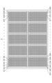
図7は、本実施形態におけるLEDモジュール3の構成を示す図である。本実施形態では、COB1からCOB10までの10個の回路基板が光源装置の筐体または筐体内の支持基板に実装されている。各COBには、チップ列が8個実装されており、各チップ列は一列に並んだ15個のLEDチップを備える。それぞれのCOBに対応する各電源が各COBへ電流を供給し、COB単位(回路基板単位)で発光を制御することができる構成となっている。また、各COBには、対応した冷却器が備えられており、冷却器の流路を冷媒が一定の流量で流されている。
FIG. 7 is a diagram showing the configuration of the
目標照度や目標発光量を変更する場合には、点灯させるCOBの数と電流値を制御する。例えば、発光量が100%(第2の発光量)である場合には、全てのCOBの全てのチップ列に1Aの電流が流れるようにする。発光量が50%(第1の発光量)である場合には、全部で10個あるCOBのうちの5個のCOBの全てのチップ列に1Aの電流が流れるようにする。すなわち5個のCOBだけを点灯する。例えば、COB1、COB7、COB3、COB9、COB5を点灯し、他のCOBを消灯する。点灯しているCOBには、発光量が100%である場合と比較して温度変化が発生しない(若しくは十分小さい変化である)。そのため、発光量の変更により生じる装置10のLEDモジュール3からの光のピーク波長の変動を抑制する(許容範囲内に抑える)ことができる。
When changing the target illuminance and the target amount of light emission, the number of COBs to be lit and the current value are controlled. For example, when the light emission amount is 100% (second light emission amount), a current of 1 A flows through all chip rows of all COBs. When the amount of light emission is 50% (the first amount of light emission), a current of 1A is caused to flow through all the chip rows of 5 COBs out of 10 COBs in total. That is, only 5 COBs are lit. For example, COB1, COB7, COB3, COB9, and COB5 are turned on, and other COBs are turned off. The COB that is lit does not change in temperature (or the change is sufficiently small) as compared with the case where the amount of light emitted is 100%. Therefore, fluctuations in the peak wavelength of the light from the
また、COBを選択的に点灯させるか否かを決定させるだけでは発光量を達成できない場合がある。例えば、10個のCOBを備えるLEDモジュール3の発光量が75%である場合、7個のCOBを全てのチップ列に1Aの電流を流して点灯させると必要な発光量を下回り、8個のCOBを全てのチップ列に1Aの電流をして点灯させると必要な発光量を上回る。そのような場合には、この8個のCOBの全てのチップ列に流れる電流値を変更することで必要な発光量となるように調整すれば良い。
In addition, there are cases where the amount of light emission cannot be achieved simply by determining whether or not to selectively light the COB. For example, when the light emission amount of the
必要な発光量が75%である場合には、例えば、8個のCOBを点灯させ、各チップ列に流れる電流値を75/80A(約0.94A)に下げることで、発光量を75%に調整することができる。このとき、点灯させるLEDチップの温度は、許容範囲以内に調整される必要がある。すなわち、点灯させるLEDチップの温度は、各チップ列に流れる電流値の低下に応じて低下するが、温度低下が許容範囲以内であれば問題はない。 If the required amount of light emission is 75%, for example, by lighting eight COBs and lowering the current value flowing through each chip row to 75/80 A (approximately 0.94 A), the amount of light emission is reduced to 75%. can be adjusted to At this time, the temperature of the LED chip to be lit needs to be adjusted within the allowable range. That is, the temperature of the LED chips to be lit decreases as the current flowing through each chip row decreases, but there is no problem if the temperature decrease is within the allowable range.
本実施形態では、点灯するグループをCOB毎としたが、複数のCOBを有する光源装置においてもチップ列単位や複数のチップ列を一つのグループにした単位で電流を流すか否かを制御しても良い。 In the present embodiment, the group to be lit is set for each COB. However, even in a light source device having a plurality of COBs, it is possible to control whether or not current is supplied in units of chip rows or in units of a plurality of chip rows grouped together. Also good.
図8は、複数のCOBを有する光源装置10において、チップ列毎に点灯を制御する例を説明するための図である。図8の光源装置10は、図7で説明した光源装置10と同様に、LEDモジュール3は、10個のCOBを備え、各COBにはチップ列S1~S80が実装されている。発光量に応じて点灯するLEDチップ1、発光量の変更前後における各LEDチップの温度変化とLEDモジュール3からの光のピーク波長の変動量は、図7で説明した光源装置10と同様である。
FIG. 8 is a diagram for explaining an example of controlling lighting for each chip row in the
また、本実施形態は、第1の発光量の場合に一部のCOB(或いは一部のチップ列)に流れる電流をゼロにする例であるが、これに限らない。例えば、発光量2(第1の発光量)の場合に所定値以上の電流を流して発光させるLEDチップの数が、発光量1(第2の発光量)の場合に所定値以上の電流を流して発光させるLEDチップの数より少なくなるようにすれば良い。すなわち、発光量2(第1の発光量)の場合に、一部のCOB(或いは一部のチップ列)に流れる電流を完全にゼロにしなくとも良く、上記の所定の電流値より小さな電流値の電流が流れていても良い。 Also, this embodiment is an example in which the current flowing through some COBs (or some chip arrays) is set to zero in the case of the first light emission amount, but the present invention is not limited to this. For example, when the amount of light emission is 2 (first amount of light emission), a current of a predetermined value or more is applied to the number of LED chips to emit light, and when the amount of light emission is 1 (second amount of light emission), a current of a predetermined value or more is applied to the number of LED chips. It is sufficient that the number of LED chips is smaller than the number of LED chips that are caused to flow and emit light. That is, when the light emission amount is 2 (the first light emission amount), the current flowing through some COBs (or some chip arrays) does not have to be completely zero. current may flow.
以上より、本実施形態では、発光量の変更により生じるLEDモジュールからの光のピーク波長の変動を抑制することができる。 As described above, in this embodiment, it is possible to suppress fluctuations in the peak wavelength of the light from the LED module caused by changes in the amount of light emitted.
<第4実施形態>
第1実施形態では、発光量に応じて電流を流すチップ列数の全チップ列数に対する割合を変更した際に、点灯させるチップ列に流す電流の電流値を変更しない例について説明した。本実施形態では、発光量に応じて電流を流すチップ列数の全チップ列数に対する割合を変更した際に、チップ列に流す電流の電流値も適切に変更する例について説明する。尚、光源装置10の構成については、第1実施形態と同様であるため説明を省略する。また、本実施形態で言及しない事項については、第1実施形態に従う。
<Fourth Embodiment>
In the first embodiment, an example has been described in which the current value of the current to be applied to the chip arrays to be lit is not changed when the ratio of the number of chip arrays to the total number of chip arrays to which current is applied according to the amount of light emission is changed. In the present embodiment, an example will be described in which the current value of the current to be passed through the chip rows is appropriately changed when the ratio of the number of the chip rows to the total number of the chip rows is changed according to the amount of light emission. Note that the configuration of the
本実施形態では、発光量1から発光量2へと発光量を小さくするときに、電流制御部9により、発光量の変更に伴い一部のLEDチップ列に電流が流れないようにすることに加え、点灯させるLEDチップ列に流れる電流の電流値を大きくする。これにより、発光量の変更に応じて発生していたLEDチップの温度の変化をより低減させることができる。
In this embodiment, when the light emission amount is decreased from
図9は本実施形態において、発光量に応じて点灯させるLEDチップ列の数及び点灯させるLEDチップ列に流す電流の電流値を変更したときのLEDチップ1の温度を示す概念図である。図9のグラフには、図5のグラフと同様に、3つの異なる発光量1~3でLEDチップ列2を点灯させた場合のLEDチップ1の位置と温度の関係が示されている。図9のグラフの上部に示す図は、光源装置10の断面図であり、LEDチップ1の位置とグラフの横軸が対応することを示している。発光量1となるようにLEDチップ列2を点灯させるためには、全てのLEDチップ列2に1Aの電流を流せば良い。
FIG. 9 is a conceptual diagram showing the temperature of the
発光量1の50%の発光量である発光量2となるようにLEDチップ列2を点灯させるためには、第1実施形態では3つのLEDチップ列2に電流が流れるようにしていたが、本実施形態では2つのLEDチップ列2に電流が流れるように電流制御部9が制御する。電流を流すチップ列を2つにすると、チップ列2に流す電流値が1AのままではLEDモジュール3に必要な発光量2を下回る発光量となるため、点灯させるチップ列に流す電流値を1Aから1.5Aに増加させる。
In order to light the
同様に、発光量1の33%の発光量である発光量3となるようにLEDチップ列2を点灯させるためには、第1実施形態では2つのチップ列に電流が流れるようにしていたが、本実施形態では1つのチップ列に電流が流れるように電流制御部9が制御する。電流を流すチップ列を1つにすると必要な発光量を下回ってしまうため、点灯させるチップ列に流す電流値に余裕がある場合には、電流値を1Aから2Aに増加させれば良い。
Similarly, in order to light the
第1実施形態において、発光量を発光量1から発光量2や3に変更した際に、点灯させるLEDチップを減らしたことにより、点灯させるLEDチップの温度も小さくなっていた。そこで、本実施形態では、電流を流すチップ列を減らした上で電流値を増加させることにより、点灯するLEDチップの発熱量を増加させ、結果的にLEDチップの温度変化が第1実施形態よりも小さくなるようにすることが可能となる。電流を流すチップ列の数及び電流値は、上記の例の限りではなく、冷媒の流れる速度等の要因により適切な値が変わるため、適宜設定されても良い。
In the first embodiment, when the light emission amount is changed from
以上より、本実施形態では、発光量の変更により生じるLEDモジュールからのピーク波長の変動を抑制することができる。 As described above, in the present embodiment, it is possible to suppress fluctuations in the peak wavelength from the LED module caused by changes in the amount of light emitted.
<露光装置の実施形態>
本実施形態では、上記第1実施形態乃至第4実施形態のいずれかの光源装置10を搭載した露光装置の一例について説明する。光源装置10の構成については、第1実施形態乃至第4実施形態のいずれかと同様であるため、説明を省略する。
<Embodiment of exposure apparatus>
In this embodiment, an example of an exposure apparatus equipped with the
図10は、本実施形態の露光装置100の構成を示す概略図である。露光装置100は、半導体デバイスや、フラットパネルディスプレイ(FPD)などのデバイスを製造する際のリソグラフィ工程に用いられる装置であり、マスク(原版)のパターンをレジスト(感光材)が塗布された基板に転写する。これにより、露光装置100は、基板上のレジストに潜像パターンを形成する。本実施形態では、ステップ・アンド・スキャン方式の露光装置について説明するが、第1実施形態乃至第4の実施形態の光源装置は、ステップ・アンド・リピート方式等他の露光方式の露光装置にも適用できる。
FIG. 10 is a schematic diagram showing the configuration of the
露光装置100は、マスクMを照明する照明光学系101、マスクステージ102、マスクMのパターンを基板W上に投影する投影光学系103、基板ステージ104、主制御部105を有する。投影光学系103は、凹面ミラーと凸面ミラーと台形ミラーとを組み合わせた反射型投影光学系であるが、後述するように他のタイプの光学系も使用できる。
The
照明光学系101は、光源装置10からの光をマスクMに照明する。マスクMには、基板Wに形成すべきパターンに対応するパターンが形成されている。マスクMは、マスクステージ102に保持されており、基板Wは、基板ステージ104に保持されている。照明光学系101は、第1コンデンサレンズ群106、ハエの目レンズ群やレンチキュラーレンズ群を備えるオプティカルインテグレータ107、第2コンデンサレンズ群108等からなる。このような構成にすることで、光源装置10からの光の光量分布が不均一であっても、ステージ102に保持したマスクMのパターン面(パターンが形成された面)において、一様な照度分布が得られる。
The illumination
主制御部105は、露光装置100の各部を制御する。例えば、主制御部105は、光源装置10の発光量の制御や、マスクステージ102及び基板ステージ104の駆動を制御する。
A
マスクMのパターン面と基板Wのレジストとは、投影光学系103を介して、光学的にほぼ共役な位置に配置されている。投影光学系103には、反射型投影光学系(収差補正用のレンズを含む場合あり)、複数のレンズを備える屈折型投影光学系、複数のレンズと凹面ミラーとを備える反射屈折型投影光学系を適用することができる。投影光学系103は、本実施形態では、所定の投影倍率を有し、マスクMに形成された回路パターンの一部を基板Wに投影する。そして、マスクステージ102及び基板ステージ104を、投影光学系103の物体面と平行な方向に、投影光学系103の投影倍率に応じた速度比で走査する。これにより、マスクMに形成された回路パターン全部を基板Wに転写することができる。
The pattern surface of the mask M and the resist of the substrate W are arranged at almost optically conjugate positions via the projection
基板Wに塗布されるレジストは、露光光の波長に応じて異なる感度を有する。そのため、レジストの感光に適した波長と、光源装置10からの光のピーク波長とが異なる(すなわち、光源装置10からの露光光のピーク波長の変動がある)場合には、後の現像工程で得られる結果に影響を与えてしまう。露光光のピーク波長の変動がある場合には、現像により得られるレジストパターンの線幅が変化してしまい、線幅の誤差が生じる。線幅の誤差は、例えば、ピーク波長の変動が2nm以内(±1nm)であれば、線幅の誤差が基準範囲内におさまるが、ピーク波長の変動が2nmより大きい場合には、基準範囲内におさまらないおそれがある。そのため、光源装置10からの光のピーク波長の変動を抑制する必要がある。
The resist applied to the substrate W has different sensitivities depending on the wavelength of the exposure light. Therefore, if the wavelength suitable for exposure of the resist is different from the peak wavelength of the light from the light source device 10 (that is, the peak wavelength of the exposure light from the
第1実施形態乃至第4の実施形態の光源装置10は、発光量の変更により生じるLEDモジュールからの光のピーク波長の変動を許容範囲内におさめることができる露光装置100を提供できる。
The
また、本実施形態では、光源には、特定のピーク波長(例えば、365nm、405nmまたは436nmのいずれか1つの波長)の光を発するLEDチップが用いられることを想定して説明したが、これに限らない。例えば、互いにピーク波長が異なる2種類のLEDチップからの光を合成した2波長合成の露光光により基板を露光しても良い。2波長合成の露光光を用いることで、露光光の光量、すなわち被露光基板上における照度を向上させることができる。 Further, in the present embodiment, the light source is described assuming that an LED chip that emits light of a specific peak wavelength (for example, any one of 365 nm, 405 nm, or 436 nm) is used. Not exclusively. For example, the substrate may be exposed with two-wavelength composite exposure light obtained by combining light from two types of LED chips having different peak wavelengths. By using the two-wavelength combined exposure light, it is possible to improve the light quantity of the exposure light, that is, the illuminance on the substrate to be exposed.
2種類のLEDチップの組合せの例として、ピーク波長が365nmの光を発する第1のLEDとピーク波長が405nmの光を発する第2のLEDとの組合せがある。この組合せを利用する場合、LEDモジュールが第1のLED群と第2のLED群とを備える形態か第1のLED群を備える第1のLEDモジュールと第2のLED群を備える第2のLEDとを用いる形態を採れる。そのような2波長合成の場合でも、それぞれのLEDチップからの光のピーク波長が変動しないように光源装置10の電流を制御することによって、現像後に得られるレジストパターンの線幅の誤差を低減させることができる。互いにピーク波長が異なる3種類以上のLEDチップからの光同士を合成した3波長合成の露光光を用いる形態としても良い。2波長の光を合成させる例として、ピーク波長が365nmの光を反射すると共にピーク波長が405nmの光は透過させるダイクロイックミラーを用いて異なる波長の光を合成できる。
An example of a combination of two types of LED chips is a combination of a first LED that emits light with a peak wavelength of 365 nm and a second LED that emits light with a peak wavelength of 405 nm. When utilizing this combination, either the LED module comprises a first group of LEDs and a second group of LEDs, or the first LED module comprises a first group of LEDs and the second group of LEDs comprises a second group of LEDs. can take the form of using Even in the case of such two-wavelength synthesis, the line width error of the resist pattern obtained after development is reduced by controlling the current of the
また、第1実施形態乃至第4実施形態において、100%、50%、33%の3段階に発光量を変えた際に波長の変動を低減できる光源装置10について説明した。この光源装置10を露光装置100に適用する場合、露光対象に応じて発光量を変更することができる。例えば、高照度の露光が必要なプロセスとして、透明電極膜(Indium Tin Oxide:ITO)の製造が挙げられる。ITOの製造で求められる光源の発光量が100%であるとき、その他のプロセスで求められる光源の発光量は、70%程度である。本実施形態における光源装置10は、発光量を100%から70%に変更した場合でも、その変更により生じうる波長変動を抑制することができる。
Further, in the first to fourth embodiments, the
また、第1実施形態乃至第4実施形態において説明した光源装置10を露光装置100に適用する場合、多数のLEDチップからの光により高い発光量を実現することが求められる。例えば、露光装置の光源として水銀ランプを適用する場合と同程度の発光量を達成することが求められる。しかしながら、LEDチップ1つ1つの発光量は水銀ランプの発光量と比較して、非常に小さい。そこで、本実施形態の光源装置10では、LEDチップが、例えば、1つの回路基板に150個以上搭載されていることが好ましい。より好ましくは、本実施形態の光源装置10として、150個以上搭載された回路基板が図7に示すように複数枚(例えば、6枚以上)構成されていることが好ましい。
Further, when the
<物品の製造方法の実施形態>
本発明の実施形態にかかる物品の製造方法は、例えば、フラットパネルディスプレイ(FPD)を製造するのに好適である。本実施形態の物品の製造方法は、基板上に塗布された感光剤に上記の露光装置100による露光で潜像パターンを形成し、露光基板を得る工程(露光工程)と、かかる工程で潜像パターンが形成された露光基板を現像し、現像基板を得る工程(現像工程)とを含む。更に、かかる製造方法は、他の周知の工程(酸化、成膜、蒸着、ドーピング、平坦化、エッチング、レジスト剥離、ダイシング、ボンディング、パッケージング等)を含む。本実施形態の物品の製造方法は、従来の方法に比べて、物品の性能・品質・生産性・生産コストの少なくとも1つにおいて有利である。
<Embodiment of method for manufacturing article>
A method for manufacturing an article according to an embodiment of the present invention is suitable for manufacturing a flat panel display (FPD), for example. The method for manufacturing an article according to the present embodiment comprises a step of obtaining an exposed substrate by forming a latent image pattern on a photosensitive agent applied on a substrate by exposure with the
以上、本発明の好ましい実施形態について説明したが、本発明はこれらの実施形態に限定されないことはいうまでもなく、その要旨の範囲内で種々の変形及び変更が可能である。 Although the preferred embodiments of the present invention have been described above, it goes without saying that the present invention is not limited to these embodiments, and various modifications and changes are possible within the scope of the gist.
1 LEDチップ(LED)
2 チップ列
3 LEDモジュール
7 制御部
8 取得部
9 電流制御部(光量変更部)
10 光源装置
11 回路基板
12 冷却器
1 LED chip (LED)
2
10
Claims (22)
前記発光量が第1の発光量の場合に所定の電流値より大きな電流を流して発光させるLEDの数が、前記発光量が前記第1の発光量より大きな第2の発光量の場合に前記所定の電流値より大きな電流を流して発光させるLEDの数より少ないことを特徴とする光源装置。 A light source device having an LED module in which a plurality of LEDs are arranged and a cooler that cools the LED module with a coolant flowing inside, wherein the light emission amount of the LED module is variable,
When the light emission amount is the first light emission amount, the number of LEDs to emit light by flowing a current larger than a predetermined current value is the second light emission amount when the light emission amount is larger than the first light emission amount. A light source device characterized in that the number of LEDs is smaller than the number of LEDs that are caused to emit light by flowing a current larger than a predetermined current value.
前記電流制御部は、前記発光量の大きさに基づいて、前記複数のLEDの全てのLEDの数に対して、前記所定の電流値より大きな電流を流して発光させるLEDの数の割合を決定することを特徴とする請求項1乃至3のいずれか1項に記載の光源装置。 further comprising a current control unit for controlling currents to flow through the plurality of LEDs;
The current control unit determines, based on the magnitude of the light emission amount, the ratio of the number of LEDs to be caused to emit light by flowing a current greater than the predetermined current value to all of the plurality of LEDs. The light source device according to any one of claims 1 to 3, characterized in that:
前記電流制御部は、前記複数個のチップ列のチップ列毎に電流制御を行うことを特徴とする請求項4乃至10のいずれか1項に記載の光源装置。 The LED module includes a plurality of chip rows in which a plurality of LEDs are arranged,
11. The light source device according to any one of claims 4 to 10, wherein the current control section controls the current for each chip row of the plurality of chip rows.
前記仕切りは、前記複数の流路が、前記複数個のチップ列のそれぞれの位置に対応して設けられることを特徴とする請求項11乃至13のいずれか1項に記載の光源装置。 The cooler includes partitions that form a plurality of flow paths through which the coolant flows,
14. The light source device according to any one of claims 11 to 13, wherein the partitions are provided so that the plurality of flow paths correspond to respective positions of the plurality of chip arrays.
前記電流制御部は、前記発光量の大きさに基づいて、前記複数の回路基板の前記複数のLEDに対する電流制御を回路基板単位で行うことを特徴とする請求項4乃至14のいずれか1項に記載の光源装置。 The LED module comprises a plurality of circuit boards on which a plurality of LEDs are arranged,
15. The current control unit according to any one of claims 4 to 14, wherein the current control unit performs current control for the plurality of LEDs of the plurality of circuit boards on a circuit board basis based on the magnitude of the light emission amount. The light source device according to .
前記電流制御部は、
前記発光量が第1の発光量の場合に第1の数の前記LEDに対して第1の電流値の電流を流し、前記発光量が前記第1の発光量より大きな第2の発光量の場合に前記第1の数より多い第2の数の前記LEDに対して第2の電流値の電流を流すときに
前記第1の数の前記LEDに関する前記第1の電流値の平均値と前記第2の数の前記LEDに関する前記第2の電流値の平均値が互いに同じか、または前記第1の電流値の平均値と前記第2の電流値の平均値の差が、前記第1の電流値の平均値と前記第2の電流値の平均値のうちの大きい方の値の20%以内になるように
前記複数のLEDに対する電流値を制御することを特徴とする光源装置。 A light source device for exposure light for exposing a photosensitive material, comprising: a plurality of LEDs for emitting the exposure light; and a current control unit for controlling current values for the plurality of LEDs in order to adjust the emission amount of the exposure light. has
The current control unit
When the light emission amount is the first light emission amount, a current of a first current value is passed through the first number of the LEDs, and the light emission amount is a second light emission amount larger than the first light emission amount. the average value of the first current values for the first number of LEDs and the The average values of the second current values for the second number of the LEDs are the same, or the difference between the average value of the first current values and the average value of the second current values is equal to the first A light source device, wherein the current values for the plurality of LEDs are controlled so as to be within 20% of the larger one of the average value of the current values and the average value of the second current values.
前記第1の数の前記LEDに関する前記第1の電流値の平均値と前記第2の数の前記LEDに関する前記第2の電流値の平均値が互いに同じか、または前記第1の電流値の平均値と前記第2の電流値の平均値の差が、前記第1の電流値の平均値と前記第2の電流値の平均値のうちの大きい方の値の10%以内になるように、
前記複数のLEDに対する電流値を制御することを特徴とする請求項16に記載の光源装置。 The current control unit
the average value of the first current values for the first number of the LEDs and the average value of the second current values for the second number of the LEDs are the same, or The difference between the average value and the average value of the second current value is within 10% of the larger value of the average value of the first current value and the average value of the second current value. ,
17. The light source device according to claim 16, wherein current values for said plurality of LEDs are controlled.
前記第1の数の前記LEDに関する前記第1の電流値のうち最大の電流値と最小の電流値の差が前記最大の電流値の20%以内であるか、または前記第1の数の前記LEDに関する前記第1の電流値が前記第1の数の前記LEDの間で互いに同じ電流値になり、
前記第2の数の前記LEDに関する前記第2の電流値のうち最大の電流値と最小の電流値の差が前記最大の電流値の20%以内であるか、または前記第1の数の前記LEDに関する前記第2の電流値が前記第2の数の前記LEDの間で互いに同じ電流値になるように、
前記複数のLEDに対する電流値を制御することを特徴とする請求項16又は17に記載の光源装置。 The current control unit
a difference between a maximum current value and a minimum current value of said first current values for said first number of said LEDs is within 20% of said maximum current value, or said first number of said wherein the first current value for the LEDs is the same among the first number of the LEDs;
a difference between a maximum current value and a minimum current value of said second current values for said second number of said LEDs is within 20% of said maximum current value, or said first number of said so that the second current value for the LEDs is the same current value among the second number of the LEDs;
18. The light source device according to claim 16, wherein current values for said plurality of LEDs are controlled.
前記光量変更部は、第1の発光量より大きな第2の発光量から前記第1の発光量に変更でき、前記第1の発光量の場合に発光させる前記LEDの数を前記第2の発光量の場合に発光させる前記LEDの数より少なくすることを特徴とする光源装置。 A light source device having 150 or more LEDs and a light amount changing unit that changes the light emission amount by changing the number of LEDs that emit light in the 150 or more LEDs,
The light amount changing unit can change from a second light emission amount larger than the first light emission amount to the first light emission amount, and changes the number of the LEDs to emit light in the case of the first light emission amount to the second light emission amount. A light source device characterized in that the number of LEDs to emit light is smaller than the number of LEDs that emit light.
前記発光量が第1の発光量の場合に所定の電流値より大きな電流を流して発光させるLEDの数が、前記発光量が前記第1の発光量より大きな第2の発光量の場合に前記所定の電流値より大きな電流を流して発光させるLEDの数より少なくなるように制御することを特徴とする制御方法。 A light source device having an LED module in which a plurality of LEDs are arranged and a cooler that cools the LED module with a cooling medium flowing therein, and controlling the light emission of the LED module in a light source device in which the light emission amount of the LED module is variable. A control method comprising:
When the light emission amount is the first light emission amount, the number of LEDs to emit light by flowing a current larger than a predetermined current value is the second light emission amount when the light emission amount is larger than the first light emission amount. A control method characterized by controlling the number of LEDs to emit light by passing a current greater than a predetermined current value.
前記露光基板を現像し、現像基板を得る現像工程と、を含み、
前記現像基板から物品を製造することを特徴とする物品の製造方法。 an exposure step of obtaining an exposed substrate by exposing the substrate using the exposure apparatus according to claim 21;
a developing step of developing the exposed substrate to obtain a developed substrate,
A method for producing an article, comprising producing an article from the developed substrate.
Priority Applications (3)
| Application Number | Priority Date | Filing Date | Title |
|---|---|---|---|
| JP2021119815A JP2023015808A (en) | 2021-07-20 | 2021-07-20 | Light source apparatus, exposure apparatus, and method for manufacturing article |
| KR1020220086362A KR20230014061A (en) | 2021-07-20 | 2022-07-13 | Light source device, exposing apparatus, and method for manufacturing article |
| CN202210835115.7A CN115639728A (en) | 2021-07-20 | 2022-07-15 | Light source device, exposure device, and method for manufacturing article |
Applications Claiming Priority (1)
| Application Number | Priority Date | Filing Date | Title |
|---|---|---|---|
| JP2021119815A JP2023015808A (en) | 2021-07-20 | 2021-07-20 | Light source apparatus, exposure apparatus, and method for manufacturing article |
Publications (1)
| Publication Number | Publication Date |
|---|---|
| JP2023015808A true JP2023015808A (en) | 2023-02-01 |
Family
ID=84939487
Family Applications (1)
| Application Number | Title | Priority Date | Filing Date |
|---|---|---|---|
| JP2021119815A Pending JP2023015808A (en) | 2021-07-20 | 2021-07-20 | Light source apparatus, exposure apparatus, and method for manufacturing article |
Country Status (3)
| Country | Link |
|---|---|
| JP (1) | JP2023015808A (en) |
| KR (1) | KR20230014061A (en) |
| CN (1) | CN115639728A (en) |
-
2021
- 2021-07-20 JP JP2021119815A patent/JP2023015808A/en active Pending
-
2022
- 2022-07-13 KR KR1020220086362A patent/KR20230014061A/en active Search and Examination
- 2022-07-15 CN CN202210835115.7A patent/CN115639728A/en active Pending
Also Published As
| Publication number | Publication date |
|---|---|
| KR20230014061A (en) | 2023-01-27 |
| CN115639728A (en) | 2023-01-24 |
Similar Documents
| Publication | Publication Date | Title |
|---|---|---|
| US20120299801A1 (en) | Light source device and image display apparatus | |
| TWI421647B (en) | Exposure device, exposure beam irradiation method and production method of a panel substrate for display | |
| TWI608309B (en) | Uv led light source module unit for exposure photolithography process and exposure photolithography apparatus used the same | |
| WO2006004135A1 (en) | Exposure apparatus and device manufacturing method | |
| US11815253B2 (en) | Light source device, cooling method, and manufacturing method for product | |
| JP2007073984A (en) | Illumination light source device, exposure device and exposure method | |
| JP2023015808A (en) | Light source apparatus, exposure apparatus, and method for manufacturing article | |
| JP2004080025A (en) | Cooling device and method therefor, and aligner therewith | |
| TWI766854B (en) | Uv led light source module unit for exposure photolithography process and exposure photolithography apparatus used the same | |
| JP7458853B2 (en) | Light source device, illumination device, and exposure device. | |
| US8454170B2 (en) | Projector and method for cooling lamps installed in projector | |
| JP6041541B2 (en) | Exposure apparatus and device manufacturing method | |
| TWI579658B (en) | Uv led light source module unit for exposure photolithography process and exposure photolithography apparatus used the same | |
| KR101761279B1 (en) | LED array light source module for exposing large area pattern and apparatus for controlling the LED array light source module | |
| JP7418128B2 (en) | Light source device, illumination device, and exposure device. | |
| JP2021193407A (en) | Light source device, exposure device and manufacturing method of articles | |
| KR20160093415A (en) | Light emitting device and exposure apparatus having the same | |
| JP2023073019A (en) | Light source device, exposure device, and article manufacturing method | |
| JP2022071584A (en) | Light source device, illumination device, exposure device, irradiation device, and article manufacturing method | |
| US20110294074A1 (en) | Exposure apparatus and exposing method using the apparatus | |
| JP7202142B2 (en) | Cooling device, light source device, exposure device, and article manufacturing method | |
| WO2024038537A1 (en) | Light source unit, illumination unit, exposure device, and exposure method | |
| JP2023096984A (en) | Exposure apparatus and manufacturing method of article | |
| JPH11354431A (en) | Projection aligner and manufacture of semiconductor device | |
| JP2023096983A (en) | Exposure apparatus, exposure method and manufacturing method of article |
Legal Events
| Date | Code | Title | Description |
|---|---|---|---|
| RD01 | Notification of change of attorney |
Free format text: JAPANESE INTERMEDIATE CODE: A7421 Effective date: 20231213 |