JP2021069061A - Photoelectric conversion device, photoelectric conversion system, mobile body, inspection method of photoelectric conversion device - Google Patents
Photoelectric conversion device, photoelectric conversion system, mobile body, inspection method of photoelectric conversion device Download PDFInfo
- Publication number
- JP2021069061A JP2021069061A JP2019194804A JP2019194804A JP2021069061A JP 2021069061 A JP2021069061 A JP 2021069061A JP 2019194804 A JP2019194804 A JP 2019194804A JP 2019194804 A JP2019194804 A JP 2019194804A JP 2021069061 A JP2021069061 A JP 2021069061A
- Authority
- JP
- Japan
- Prior art keywords
- photoelectric conversion
- conversion device
- pulse signal
- counter
- circuit
- Prior art date
- Legal status (The legal status is an assumption and is not a legal conclusion. Google has not performed a legal analysis and makes no representation as to the accuracy of the status listed.)
- Granted
Links
- 238000006243 chemical reaction Methods 0.000 title claims abstract description 91
- 238000007689 inspection Methods 0.000 title claims abstract description 24
- 238000000034 method Methods 0.000 title claims abstract description 10
- 238000007493 shaping process Methods 0.000 claims abstract description 17
- 238000012545 processing Methods 0.000 claims description 15
- 238000012546 transfer Methods 0.000 description 21
- 238000010791 quenching Methods 0.000 description 19
- 238000003384 imaging method Methods 0.000 description 16
- 230000008859 change Effects 0.000 description 8
- 238000012360 testing method Methods 0.000 description 8
- 238000010586 diagram Methods 0.000 description 7
- 239000004065 semiconductor Substances 0.000 description 6
- 230000007423 decrease Effects 0.000 description 4
- 230000003287 optical effect Effects 0.000 description 4
- 230000000171 quenching effect Effects 0.000 description 4
- 230000015556 catabolic process Effects 0.000 description 3
- 230000004044 response Effects 0.000 description 3
- 239000000758 substrate Substances 0.000 description 3
- 230000002950 deficient Effects 0.000 description 2
- 230000006870 function Effects 0.000 description 2
- 230000003071 parasitic effect Effects 0.000 description 2
- 230000004888 barrier function Effects 0.000 description 1
- 238000007906 compression Methods 0.000 description 1
- 230000006835 compression Effects 0.000 description 1
- 238000012937 correction Methods 0.000 description 1
- 238000001514 detection method Methods 0.000 description 1
- 238000004519 manufacturing process Methods 0.000 description 1
- 239000011159 matrix material Substances 0.000 description 1
- 238000005259 measurement Methods 0.000 description 1
- 238000012986 modification Methods 0.000 description 1
- 230000004048 modification Effects 0.000 description 1
- 229910021420 polycrystalline silicon Inorganic materials 0.000 description 1
- 229920005591 polysilicon Polymers 0.000 description 1
- 230000008569 process Effects 0.000 description 1
Images


Classifications
-
- G—PHYSICS
- G01—MEASURING; TESTING
- G01J—MEASUREMENT OF INTENSITY, VELOCITY, SPECTRAL CONTENT, POLARISATION, PHASE OR PULSE CHARACTERISTICS OF INFRARED, VISIBLE OR ULTRAVIOLET LIGHT; COLORIMETRY; RADIATION PYROMETRY
- G01J1/00—Photometry, e.g. photographic exposure meter
- G01J1/42—Photometry, e.g. photographic exposure meter using electric radiation detectors
- G01J1/44—Electric circuits
-
- G—PHYSICS
- G01—MEASURING; TESTING
- G01J—MEASUREMENT OF INTENSITY, VELOCITY, SPECTRAL CONTENT, POLARISATION, PHASE OR PULSE CHARACTERISTICS OF INFRARED, VISIBLE OR ULTRAVIOLET LIGHT; COLORIMETRY; RADIATION PYROMETRY
- G01J1/00—Photometry, e.g. photographic exposure meter
- G01J1/02—Details
- G01J1/0228—Control of working procedures; Failure detection; Spectral bandwidth calculation
-
- G—PHYSICS
- G01—MEASURING; TESTING
- G01J—MEASUREMENT OF INTENSITY, VELOCITY, SPECTRAL CONTENT, POLARISATION, PHASE OR PULSE CHARACTERISTICS OF INFRARED, VISIBLE OR ULTRAVIOLET LIGHT; COLORIMETRY; RADIATION PYROMETRY
- G01J1/00—Photometry, e.g. photographic exposure meter
- G01J1/42—Photometry, e.g. photographic exposure meter using electric radiation detectors
- G01J1/44—Electric circuits
- G01J2001/4446—Type of detector
- G01J2001/446—Photodiode
- G01J2001/4466—Avalanche
Abstract
Description
本発明は、光電変換装置、光電変換システム、移動体、光電変換装置の検査方法に関する。 The present invention relates to a photoelectric conversion device, a photoelectric conversion system, a mobile body, and a method for inspecting a photoelectric conversion device.
アバランシェ増倍を行う光電変換部を有する光電変換装置が知られている。 A photoelectric conversion device having a photoelectric conversion unit that multiplies an avalanche is known.
特許文献1に記載の光電変換装置は、フォトンが光電変換部に入射したことによって生じる電子をアバランシェ増倍させ、パルス波を生成させる。このパルス波をカウンタが数えることによって、光電変換部に入射したフォトンの数をカウントすることができる。
The photoelectric conversion device described in
特許文献1では、光電変換装置を検査する構成について検討が為されていない。
本発明は、アバランシェダイオードを備える光電変換装置の検査を好適に行うことができる構成、システム、検査方法を提供する。 The present invention provides a configuration, a system, and an inspection method capable of suitably inspecting a photoelectric conversion device including an avalanche diode.
本発明は上記の課題を鑑みて為されたものであり、一の態様は、入射光に基づいてアバランシェ増倍が生じるアバランシェダイオードと、前記アバランシェダイオードが出力する信号に基づく第1パルス信号を生成する波形整形回路と、前記入射光によらず、第2パルス信号を生成する参照回路と、前記波形整形回路と前記参照回路とに接続されたカウンタとを有することを特徴とする光電変換装置である。 The present invention has been made in view of the above problems, and one aspect is to generate an avalanche diode in which an avalanche multiplication occurs based on incident light and a first pulse signal based on a signal output by the avalanche diode. A photoelectric conversion device having a waveform shaping circuit to be used, a reference circuit for generating a second pulse signal regardless of the incident light, and a counter connected to the waveform shaping circuit and the reference circuit. is there.
別の一の態様は、入射光に基づいてアバランシェ増倍が生じるアバランシェダイオードと、前記アバランシェダイオードが出力する信号に基づく第1パルス信号を生成する波形整形回路と、前記入射光によらず、第2パルス信号を生成する参照回路と、前記第1パルス信号と前記第2パルス信号とをカウントするカウンタとを有することを特徴とする光電変換装置である。 Another aspect is an avalanche diode in which an avalanche multiplier is generated based on the incident light, a waveform shaping circuit that generates a first pulse signal based on a signal output by the avalanche diode, and a first regardless of the incident light. The photoelectric conversion device is characterized by having a reference circuit for generating a two-pulse signal and a counter for counting the first pulse signal and the second pulse signal.
別の一の態様は、入射光に基づいてアバランシェ増倍が生じるアバランシェダイオードと、前記アバランシェダイオードが出力する信号に基づく第1パルス信号を生成する波形整形回路と、第1パルス信号をカウントするカウンタとを有する光電変換装置の検査方法であって、前記カウンタに、入射光によらない第2パルス信号をカウントさせ、前記カウンタが前記第2パルス信号をカウントして得られたデジタル信号と、期待値とを比較することによって、前記光電変換装置が正常であるか否かを検査することを特徴とする光電変換装置の検査方法である。 Another aspect is an avalanche diode that multiplies the avalanche based on the incident light, a waveform shaping circuit that generates a first pulse signal based on the signal output by the avalanche diode, and a counter that counts the first pulse signal. This is an inspection method for a photoelectric conversion device having the above, and is expected to be a digital signal obtained by causing the counter to count a second pulse signal that does not depend on incident light and the counter counting the second pulse signal. A method for inspecting a photoelectric conversion device, which comprises inspecting whether or not the photoelectric conversion device is normal by comparing with a value.
本発明により、光電変換装置の検査を好適に行うことができる。 According to the present invention, the photoelectric conversion device can be suitably inspected.
以下、図面を参照しながら各実施形態を説明する。 Hereinafter, each embodiment will be described with reference to the drawings.
以下に述べる各実施形態では、光電変換装置の一例として、撮像装置を中心に説明する。ただし、各実施形態は、撮像装置に限られるものではなく、光電変換装置の他の例にも適用可能である。例えば、測距装置(焦点検出やTOF(Time Of Flight)を用いた距離測定等の装置)、測光装置(入射光量の測定等の装置)などがある。 In each of the embodiments described below, an image pickup apparatus will be mainly described as an example of the photoelectric conversion apparatus. However, each embodiment is not limited to the imaging device, and can be applied to other examples of the photoelectric conversion device. For example, there are a distance measuring device (a device for measuring a distance using focus detection and TOF (Time Of Flight)), a photometric device (a device for measuring an incident light amount, etc.), and the like.
なお、以下に述べる実施形態に記載されるトランジスタの導電型は一例のものであって、実施例中に記載された導電型のみに限定されるものでは無い。実施形態中に記載された導電型に対し、導電型は適宜変更できるし、この変更に伴って、トランジスタのゲート、ソース、ドレインの電位は適宜変更される。 The conductive type of the transistor described in the embodiments described below is an example, and is not limited to the conductive type described in the examples. The conductive type can be appropriately changed with respect to the conductive type described in the embodiment, and the potentials of the gate, source, and drain of the transistor are appropriately changed with this change.
例えば、スイッチとして動作させるトランジスタであれば、ゲートに供給する電位のローレベルとハイレベルとを、導電型の変更に伴って、実施例中の説明に対し逆転させるようにすればよい。また、以下に述べる実施例中に記載される半導体領域の導電型についても一例のものであって、実施例中に記載された導電型のみに限定されるものでは無い。実施例中に記載された導電型に対し、導電型は適宜変更できるし、この変更に伴って、半導体領域の電位は適宜変更される。 For example, in the case of a transistor that operates as a switch, the low level and the high level of the potential supplied to the gate may be reversed with respect to the description in the examples as the conductive type is changed. Further, the conductive type of the semiconductor region described in the examples described below is also an example, and is not limited to the conductive type described in the examples. The conductive type can be appropriately changed with respect to the conductive type described in the examples, and the potential in the semiconductor region is appropriately changed with this change.
(第1実施形態)
第1実施形態による撮像装置について、図1、図2および図3を用いて説明する。図1は、本実施形態による撮像装置を示すブロック図である。
(First Embodiment)
The image pickup apparatus according to the first embodiment will be described with reference to FIGS. 1, 2 and 3. FIG. 1 is a block diagram showing an imaging device according to the present embodiment.
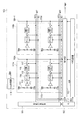
図1に示すように、本実施形態による撮像装置100は、垂直走査回路101と、タイミングジェネレータ(TG:Timing Generator)102と、列メモリ部103と、水平走査回路104とを備えている。また、撮像装置100は、行列状に配置された複数の画素回路110を備えている。ここでは、簡略化のため、4つの画素回路110a、110b、110c、110dを図示している。他の例として、さらに多くの画素回路110が撮像装置に備えられていてもよい。例えば、数千行、数千列にわたって画素回路110を配することもできる。
As shown in FIG. 1, the
TG102は、撮像装置100の各部を制御するための信号を生成する制御回路である。TG102は、垂直走査回路101、列メモリ部103に対して各種の制御信号等を供給する。また、TG102は、水平走査回路104に対して制御信号HCLKを供給する。さらに、TG102は、各々の画素回路110に対して、転送制御信号WRT、及び、リセット制御信号RESをそれぞれ供給する。
The
各々の画素回路110は、アバランシェダイオード(以下、AVDとする)111、クエンチ素子112、波形整形回路の一例であるインバータ113、カウンタ114、転送スイッチ115、画素メモリ116、行選択スイッチ117を有する。
Each pixel circuit 110 includes an avalanche diode (hereinafter referred to as AVD) 111, a
クエンチ素子112の一方のノードは、AVD111に接続される。そして、クエンチ素子112の他方のノードにはVbiasノードが接続される。AVD111には、クエンチ素子112を介してAVD111の降伏電圧より大きいバイアス電圧がVbiasノードから印加される。これにより、AVD111に光子(フォトン)が入射するとアバランシェ増倍現象が生じる。つまり、AVD111はVbiasノードから供給されるバイアス電圧が印加されることによって、ガイガーモードで動作する。
One node of the
アバランシェ増倍現象によってアバランシェ電流が生じると、クエンチ素子112において電圧降下が生じ、AVD111のカソード電位が低下する。カソード電位がAVD111の降伏電圧以下になるとアバランシェ増倍現象が停止する。その結果、アバランシェ電流が流れなくなり、AVD111のカソードには、Vbiasノードからのバイアス電圧が印加される。クエンチ素子112は、AVD111のアバランシェ増倍現象を停止させるための抵抗素子である。この抵抗素子は、MOSトランジスタで構成してもよいし、ポリシリコンなどの導電膜で構成してもよい。
When an avalanche current is generated by the avalanche multiplication phenomenon, a voltage drop occurs in the
Vbiasノードのバイアス電圧は、例えば+20V程度とすることができるが、これに限定されるものではない。例えば、AVD111のアノードを負の電位に接続するようにしてもよい。つまり、上述したようにAVD111のアノードとカソードの電位差は降伏電圧よりも大きい電圧となっていればよく、本実施形態では20V以上になるようにしている。
The bias voltage of the Vbias node can be, for example, about + 20V, but is not limited to this. For example, the anode of the AVD 111 may be connected to a negative potential. That is, as described above, the potential difference between the anode and the cathode of the
上記、バイアス電圧はVbias生成回路118により生成される。Vbias生成回路118は撮像装置100の外部に設けている。つまり、バイアス電圧は、撮像装置100の外部より供給されている。なお、撮像装置100の内部でバイアス電圧を生成するようにしても良い。
The bias voltage is generated by the Vbias
AVD111のカソードは、インバータ113の入力ノードに接続される。AVD111に光子が入射することでアバランシェ増倍が生じると、AVD111のカソードの電位が低下する(アバランシェ動作)。このカソードの電位の低下によって、インバータ113の出力が変化する。具体的には、まず定常状態ではインバータ113の入力ノードはVbiasノードから供給されるバイアス電圧となっている。そして、アバランシェ増倍によって生じる電流(以下、アバランシェ電流)により、カソードの電位が低下し、インバータ113の閾値以下となる。これにより、インバータ113の出力が変化する。また、カソードの電位が低下することによって、アノード・カソード間の電位差が降伏電圧未満となって、AVD111は非ガイガーモードとなる。よって、AVD111にはアバランシェ電流が流れなくなる。その後、AVD111のカソードの電位はVbiasノードから供給されるバイアス電圧と、クエンチ素子112とによって供給される電流によって、次第にバイアス電圧に戻る(復帰動作)。これにより、インバータ113の出力は再び変化する。このように、AVD111ではアバランシェ動作と、復帰動作とが繰り返される。また、インバータ113は、入力ノードの電位、つまりAVD111のカソードの電位の変化に基づいて、パルス信号を生成している。つまり、インバータ113は、AVD111のカソードの電位をパルス信号に変換する波形整形回路である。また、AVD111に入射する光子に基づいてインバータ113が生成するパルス信号を第1パルス信号とする。
The cathode of the AVD 111 is connected to the input node of the
カウンタ114は、インバータ113から出力されるパルス信号のパルス数をカウントする。カウンタ114のビット幅(ビット数)は、例えば16である。ビット幅が16のカウンタ114のカウント値の上限は10進数表記で65535となる。カウンタ114には、TG102からリセット制御信号RESが入力される。カウンタ114のカウント値は、リセット制御信号RESによってリセットされる。カウンタ114は、所定期間、第1パルス信号をカウントする。これにより、当該所定期間にAVD111に入射した光子の数に対応するカウント値を、デジタル信号として得ることができる。
The
転送スイッチ115は、TG102から出力される転送制御信号WRTによって制御される。転送制御信号WRTがHighレベルになると、転送スイッチ115がオンする。これにより、カウンタ114が保持したデジタル信号が、画素メモリ116に転送される。画素回路110が画素メモリ116を備えることによって、各行の画素メモリ116からデジタル信号を読み出す走査を行う期間に、カウンタ114によるカウント動作を行うことができる。これにより、高フレームレート化を実現できる。また、カウントを行うことができない不感期間を設けることなく、グローバルシャッタを行うことが可能である。なぜなら、画素メモリ116を設けない場合には、カウンタ114が保持したデジタル信号の読出しが終了するまでは、次のカウント動作を行うことができない。このため、グローバルシャッタを行う場合には、すべての画素回路110のカウンタ114からのデジタル信号の読出しが終了するまで待機する、不感期間を設ける必要がある。一方、画素回路110に画素メモリ116を設けたことによって、画素回路110からのデジタル信号の読出しの終了を待たずにカウンタ114が次のカウント動作を行うことができる。よって、不感期間を設けずにグローバルシャッタを実現することができる。
The
垂直走査回路101には、画素回路110の行ごとに配された読出し制御線READが接続される。
A read control line READ arranged for each line of the pixel circuit 110 is connected to the
読出し制御線READは、行選択スイッチ117を制御する。読み出し制御線READがHighレベルになると、行選択スイッチ117がオンする。これにより、画素メモリ116から垂直信号線105へのデジタル信号の読出しが行われる。垂直走査回路101による垂直走査により、順次、画素回路110の行ごとにデジタル信号の読出しが行われる。なお、選択される行は必ずしも1行である必要はない。例えば、垂直信号線105を1列の画素回路110に対して複数本備える場合には、複数行を同時に選択することも可能である。
The read control line READ controls the
また、図1では垂直信号線105は、デジタル信号を伝送するバスとして1本の線で簡略化して示している。垂直信号線105は、画素メモリ116からパラレル転送でデジタル信号を読み出す場合には、カウンタ114および画素メモリ116のビット幅に応じた本数が必要となる。例えば、カウンタ114のビット幅が16ビットの場合には、垂直信号線105n、105n+1はそれぞれ16本設けられる。なお、デジタル信号をシリアル転送で画素メモリ116から読出す場合には、垂直信号線105を1本の信号線で構成することも可能である。また、パラレル転送であっても、複数のグループに分割して読み出す場合には、垂直信号線105を16本設ける必要はない。
Further, in FIG. 1, the vertical signal line 105 is simplified by one line as a bus for transmitting a digital signal. When reading a digital signal from the
列メモリ部103には、複数の垂直信号線105が接続されている。個々の信号線について説明するため、複数の垂直信号線105のうち、2つの垂直信号線105n,105n+1を用いることとする。垂直信号線105n,105n+1はそれぞれ、列メモリ部103に接続される。列メモリ部103は、各々の画素回路110から読み出された各列の画素信号値をそれぞれ保持する。
A plurality of vertical signal lines 105 are connected to the
水平走査回路104は、TG102より入力される制御信号HCLKに基づき、列メモリ部103に保持された各々の列のデジタル信号を、出力線Outputを介して順次出力する。
The
以上が、各画素回路110による、入射光に基づくデジタル信号の生成と、各画素回路110からのデジタル信号の読出し動作である。この入射光に基づくデジタル信号の生成、読出しの動作を「通常動作」と表記することとする。 The above is the generation of the digital signal based on the incident light by each pixel circuit 110 and the operation of reading the digital signal from each pixel circuit 110. The operation of generating and reading a digital signal based on this incident light is referred to as "normal operation".
次に、本実施形態における、画素回路110の検査時の動作について説明する。 Next, the operation of the pixel circuit 110 at the time of inspection in the present embodiment will be described.
上述したように、AVD111のカソード・アノード間の電位差が降伏電圧以下であると、AVD111は非ガイガーモードとなる。検査時、Vbias生成回路118は、AVD111が非ガイガーモードとなる電圧で、かつインバータ113のしきい値を越える電圧で振幅するパルス信号を入力する。この検査モード時にVbias生成回路118が出力するパルス信号を第2パルス信号とする。また、第2パルス信号を出力するVbias生成回路118は、入射光によらないパルス信号である第2パルス信号を出力する参照回路である。Vbias生成回路118には、不図示のクロックパルス生成部からクロックパルスが入力される。このクロックパルスを用いて、Vbias生成回路118は第2パルス信号を生成する。なお、第2パルス信号の周期はクロックパルスと一致するものであっても良いし、クロックパルスを分周したものであっても良い。また、TG102がクロックパルスをVbias生成回路118に供給するようにしても良い。本実施形態では、第2パルス信号は、単一の周期で繰り返されるパルス波としている。ただし、この例に限定されるものではなく、第2パルス信号の周期を一定にしなくてもよい。
As described above, when the potential difference between the cathode and the anode of the
インバータ113は、Vbiasノードに入力されるパルス信号に対応して反転動作を繰り返し、カウンタ114にはインバータ113の出力の変化回数に応じたカウント値が書き込まれる。すなわち、Vbiasノードに入力したパルス数に応じたカウント値(参照デジタル信号)がカウンタ114に書き込まれる。その後、通常動作と同様に、カウンタ114が保持した参照デジタル信号が画素メモリ116に転送される。その後、通常動作と同様の垂直走査によって、出力線Outputより各画素回路110の参照デジタル信号を順次読み出す。
The
この出力線Outputから出力された参照デジタル信号と、参照デジタル信号の期待値、つまりカウンタ114が第2パルス信号をカウントする期間の開始から終了までにおける第2パルス信号のパルス数とを、撮像装置の外部の比較回路が比較する。これにより、各画素回路110が正しく動作しているかどうかを検査することができる。なお、この比較回路は、撮像装置の内部に設けてもよい。比較回路を撮像装置の内部に設けた場合には、撮像装置はBuilt−In Self Test(BIST)を備える装置として構成されることとなる。
The image pickup apparatus captures the reference digital signal output from the output line Output and the expected value of the reference digital signal, that is, the number of pulses of the second pulse signal from the start to the end of the period in which the
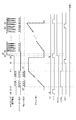
図2は、本実施形態における撮像装置100の通常動作時および、検査時の動作の詳細を示すタイミングチャートである。ここでは、複数の画素回路110のうち、画素回路110aについて説明する。
FIG. 2 is a timing chart showing details of the operation of the
図2では検査時の動作と1フレーム分の通常動作時の動作を示す。時刻t210から時刻t214までの期間は、画素回路110の検査を行う検査期間に対応する。 FIG. 2 shows an operation during inspection and an operation during normal operation for one frame. The period from the time t210 to the time t214 corresponds to the inspection period for inspecting the pixel circuit 110.
一方、時刻t216から時刻t221までの期間は通常動作を行う通常動作期間(以下、受光期間と表記することもある)に対応する。 On the other hand, the period from the time t216 to the time t221 corresponds to the normal operation period in which the normal operation is performed (hereinafter, may be referred to as a light receiving period).
まず、時刻t210において、同期信号VDがHighレベルになると、TG102は時刻t210にてリセット制御信号RESをHighレベルにする。リセット制御信号RESをHighレベルにすることにより、カウンタ114がリセット状態となる。なお、図2に示した動作では、すべての画素回路110が一括して制御される形態を示している。よって、撮像装置が備えるすべての画素回路110のカウンタ114が一斉にリセットされる。Vbias生成回路118からは、AVD111のカソードに電圧Vaが印加される。ここで、電圧VaはAVD111が非ガイガーモードであり、かつインバータ113のしきい値以上の電圧である。
First, when the synchronization signal VD reaches the high level at time t210, the
時刻t212において、リセット制御信号RESがLowレベルになるとカウンタ114のリセットが解除される。これにより、すべての画素回路110のカウンタ114は、カウント開始可能な状態(イネーブル状態)となる。
At time t212, when the reset control signal RES reaches the Low level, the reset of the
時刻t213より、Vbiasノードを接地電圧から電圧Vaの範囲でパルス駆動させる。Vbiasノードがパルス駆動されると、そのVbiasノードの電位変化に対応して、インバータ113の出力もまた変化を繰り返す。カウンタ114はインバータ113の出力が変化した回数に応じたカウント値を生成する。Vbiasノードがパルス駆動される期間、つまり時刻t213より時刻t214までの期間が、カウンタ114にテストカウント値(参照デジタル信号)を書き込むための書き込み期間となる。
From time t213, the Vbias node is pulse-driven in the range from the ground voltage to the voltage Va. When the Vbias node is pulse-driven, the output of the
時刻t215にて、TG102は転送制御信号WRTをHighレベルにする。転送制御信号WRTがHighレベルになると、転送スイッチ115がオンとなる。よって、時刻t215におけるテストカウント値(参照デジタル信号)が画素メモリ116に書き込まれる。
At time t215, the
画素メモリ116に書き込まれた参照デジタル信号の読出しは以下の動作で行われる。
The reference digital signal written in the
まず、時刻t217において、垂直走査回路101が読み出し制御信号READ1をHighレベルにする。これにより、1番目の行に位置する複数の画素回路110の各々の行選択スイッチ117がオンとなる。よって、画素メモリ116で保持された値が、各画素回路110に対応する垂直信号線105を介して列メモリ部103へと書き込まれる。
First, at time t217, the
垂直走査回路101により、以降READ2からREADnまでが順次制御される。これにより、参照デジタル信号が行ごとに順次出力される、垂直走査が行われる。
From then on, READ2 to READn are sequentially controlled by the
時刻t218から、TG102より入力される制御信号HCLKに基づき、水平走査回路104が、複数の列メモリ部103の水平走査を行う。これにより、複数の画素回路110の各々に第2パルス信号のパルス数に応じて書き込まれたテストカウント値(参照デジタル信号)が、出力線Outputを介して撮像装置100の外部の比較回路に出力される。比較回路は上述したように、各画素回路110の参照デジタル信号と期待値との比較を行う。比較回路は参照デジタル信号と期待値が一致していれば正常な画素回路110であると判定する。一方、参照デジタル信号と期待値とが不一致の場合には、不良な画素回路110であると判定する。これにより、各画素回路110が正常であるか検査を行うことができる。なお、不良な画素回路110については、その画素回路110のアドレスを特定することによって、通常動作時には不使用とすることもできる。
From time t218, the
次に、通常動作時の駆動について説明する。 Next, the drive during normal operation will be described.
時刻t216に同期信号VDがHighレベルとなると、TG102はリセット制御信号RESをHighレベルにする。リセット制御信号RESがHighレベルとなることにより、各画素回路110のカウンタ114はリセット状態となる。こうして各々の画素回路110のカウンタ114に保持されていた参照デジタル信号は一斉にリセットされる。
When the synchronization signal VD reaches the high level at time t216, the
時刻t219に、Vbiasノードの電位が20Vに上昇する。これにより、AVD111はガイガーモードとなる。光子(フォトン)が入射するとアバランシェ増倍現象を引き起こす状態となる。本実施例ではVbiasを20Vとしているが、ガイガーモードに移行する電圧が与えられればよい。また、AVD111のアノードに負電圧を与えてもよい。
At time t219, the potential of the Vbias node rises to 20V. As a result, the
リセット制御信号RESがLowレベルになると、カウンタ114のリセットが解除され、カウント開始可能な状態となる。
When the reset control signal RES reaches the Low level, the reset of the
時刻t220に入射光による光子がAVD111に入射すると、アバランシェ電流が発生する。クエンチ素子112での電圧降下によりAVD111のカソードの電位が低下する。これにより、インバータ113の出力が変化する。アバランシェ電流が停止すると、クエンチ素子112を介してVbiasノードから供給されるバイアス電圧により、AVD111のカソードの電位は20Vに復帰する。これにより、インバータ113の出力は再び変化する。典型的には、AVD111への光子1個の入射により、インバータ113は1パルスを発生する。以後、光子がAVD111に入射する都度、同様のアバランシェ増倍動作、復帰動作を繰り返す。この動作の繰り返しによって生じたパルス数に応じて、カウンタ114のカウント値が変化する。
When a photon due to incident light is incident on AVD111 at time t220, an avalanche current is generated. The voltage drop at the quench
時刻t221にて、転送制御信号WRTがHighレベルになると、転送スイッチ115がオンとなり、時刻t221におけるカウント値が画素メモリ116に書き込まれる。
When the transfer control signal WRT reaches the High level at time t221, the
画素メモリ116からの読出しは上述の検査時と同様に、垂直走査回路101により、読出し行が順次選択される。垂直信号線105を介して、列メモリ部103へと転送される。その後、水平走査回路104の動作により順次Outputを介して出力される。
For reading from the
以上の通り、本発明によれば、Vbias生成回路118が供給する電圧を通常動作時と検査時とで変更することによって、画素回路110の構成を変更することなく、画素回路110の検査を行うことができる。
As described above, according to the present invention, the pixel circuit 110 is inspected without changing the configuration of the pixel circuit 110 by changing the voltage supplied by the
なお、本実施形態では、検査動作、通常動作の順に動作させた場合を説明した。検査動作を常に行う必要はなく、例えば、撮像装置100の製造時に検査を行うようにしても良い。また、検査動作を、所定の動作時間を経過するごとに、繰り返し行うようにしても良い。
In this embodiment, the case where the inspection operation and the normal operation are performed in this order has been described. It is not always necessary to perform the inspection operation, and for example, the inspection may be performed at the time of manufacturing the
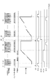
また、本実施形態の構成を利用して、画素回路110の通常動作の機能を拡張することもできる。例えば、通常動作時に生成するカウント値にオフセットを付与することができる。このオフセットの付与動作の例を、図3に示す。 Further, the function of the normal operation of the pixel circuit 110 can be extended by using the configuration of the present embodiment. For example, an offset can be added to the count value generated during normal operation. An example of this offset giving operation is shown in FIG.
まず、時刻t210に、同期信号VDがHighレベルになると、TG102はリセット制御信号RESをHighレベルにする。これにより、各画素回路110のカウンタ114がリセット状態となる。
First, when the synchronization signal VD reaches the high level at time t210, the
時刻t211に、Vbias生成回路118から、AVD111のカソードに電圧Vaが印加される。ここで、電圧VaはAVD111が非ガイガーモードとなり、かつインバータ113のしきい値以上の電圧である。
At time t211 the voltage Va is applied to the cathode of the
時刻t212において、リセット制御信号RESがLowレベルになるとカウンタ114のリセットが解除され、カウント動作可能な状態(イネーブル状態)となる。
At time t212, when the reset control signal RES reaches the Low level, the reset of the
時刻t213から、Vbiasノードを接地電圧から電圧Vaの範囲でパルス駆動させる。Vbiasノードがパルス駆動されると、そのVbiasノードの電位変化に対応して、インバータ113の出力もまた変化を繰り返す。カウンタ114はインバータ113の出力が変化した回数に応じたカウント値を生成する。Vbiasノードがパルス駆動される期間、つまり時刻t213から時刻t214までの期間が、カウンタ114にテストカウント値(参照デジタル信号)を書き込むための書き込み期間となる。
From time t213, the Vbias node is pulse-driven in the range of voltage Va from the ground voltage. When the Vbias node is pulse-driven, the output of the
そして、時刻t215に、Vbiasノードの電位が20Vに上昇する。これにより、AVD111はガイガーモードとなる。光子(フォトン)が入射するとアバランシェ増倍現象を引き起こす状態となる。本実施例ではVbiasを20Vとしているが、ガイガーモードに移行する電圧が与えられればよい。また、AVD111のアノードに負電圧を与えてもよい。
Then, at time t215, the potential of the Vbias node rises to 20V. As a result, the
時刻t216に入射光による光子がAVD111に入射すると、アバランシェ電流が発生する。クエンチ素子112での電圧降下によりAVD111のカソードの電位が低下する。これにより、インバータ113の出力が変化する。アバランシェ電流が停止すると、クエンチ素子112を介してVbiasノードから供給されるバイアス電圧により、AVD111のカソードの電位は20Vに復帰する。これにより、インバータ113の出力は再び変化する。典型的には、AVD111への光子1個の入射により、インバータ113は1パルスを発生する。以後、光子がAVD111に入射する都度、同様のアバランシェ増倍動作、復帰動作を繰り返す。この動作の繰り返しによって生じたパルス数に応じて、カウンタ114のカウント値が変化する。
When a photon due to incident light is incident on AVD111 at time t216, an avalanche current is generated. The voltage drop at the quench
時刻t217に、Vbiasノードに電圧Vaが与えられ、AVD111は非ガイガーモードとなる。時刻t215から時刻t217までは入射光に対応するデジタル信号取得期間となる。 At time t217, a voltage Va is applied to the Vbias node and the AVD111 goes into non-Geiger mode. The period from time t215 to time t217 is the digital signal acquisition period corresponding to the incident light.
時刻t218に、転送制御信号WRTがHighレベルになると、転送スイッチ115がオンとなる。よって時刻t218におけるカウント値が画素メモリ116に書き込まれる。ここで、書き込まれる信号は、(既知のオフセット信号)と(画素信号)の和となる。
When the transfer control signal WRT reaches the High level at time t218, the
画素メモリ116からの読み出しは上述の動作同様に、垂直走査回路101により、読み出し行が順次選択され、垂直信号線105を介して、列メモリ部103へと転送される。その後、水平走査回路104の動作により順次Outputを介して出力される。
As for the reading from the
以上の通り、アバランシェ電流を発生させない非ガイガーモードにおいて、Vbiasノードをパルス駆動することで、入射光に基づくデジタル信号に対し、所定の値のオフセットを付与することが可能となる。 As described above, in the non-Geiger mode in which the avalanche current is not generated, by pulse-driving the Vbias node, it is possible to give an offset of a predetermined value to the digital signal based on the incident light.
本実施形態の構成によれば、画素回路110の構成を変更せず検査を実施することができる。また、通常動作時に生成するデジタル信号に対し、所定の値のオフセットを付与することができる。 According to the configuration of the present embodiment, the inspection can be performed without changing the configuration of the pixel circuit 110. Further, an offset of a predetermined value can be added to the digital signal generated during normal operation.
(第2実施形態)
本実施形態について、第1実施形態と異なる点を中心に説明する。
(Second Embodiment)
The present embodiment will be described focusing on the differences from the first embodiment.
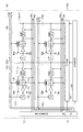
図4は、本実施形態の撮像装置(光電変換装置の一例)の構成を示した図である。 FIG. 4 is a diagram showing a configuration of an imaging device (an example of a photoelectric conversion device) of the present embodiment.
複数の画素回路110のそれぞれは、クエンチ素子であるPMOSトランジスタ1120と、PMOSトランジスタ1120のゲートに接続されたクエンチ制御部120とを有する。複数の画素回路110の各々のクエンチ制御部120は、TG102に接続されている。
Each of the plurality of pixel circuits 110 has a
また、複数の画素回路110のそれぞれは、パルス生成回路119を有する。なお、図面では、パルス生成回路をPG(Pulse Generator)として示している。以下、パルス生成回路119をPG119と表記することもある。パルス生成回路119は、本実施形態における、入射光によらない第2パルス信号を生成する参照回路である。
Further, each of the plurality of pixel circuits 110 has a
複数の画素回路110のそれぞれのPG119はTG102からの制御信号PCTRLにより制御される。制御信号PCTRLがHighレベルになると、PG119は入射光によらないパルス信号(第2パルス信号)を出力する。PG119が出力するパルス信号は、インバータ113の入力ノードに入力される。制御信号PCTRLがLowレベルになると、PG119の出力はハイインピーダンスとなり、第2パルス信号の出力が停止される。また、複数の画素回路110の各々のPG119は、TG102から供給される不図示のクロックパルスを用いて、第2パルス信号を生成する。第2パルス信号の周期は、クロックパルスの周期と一致するものであっても良いし、所定の周期に分周されたものであっても良い。
Each PG119 of the plurality of pixel circuits 110 is controlled by the control signal PCTRL from the TG102. When the control signal PCTRL reaches the High level, the PG119 outputs a pulse signal (second pulse signal) that does not depend on the incident light. The pulse signal output by the
複数の画素回路110の各々のクエンチ制御部120は、TG102からの制御信号RCTRLにより制御される。この制御信号RCTRLによって、PMOSトランジスタ1120のソース・ドレイン間の抵抗値が制御される。制御信号RCTRLがLowレベルの場合には、PMOSトランジスタ1120はクエンチ素子として機能する。一方、制御信号RCTRLがHighレベルの場合には、PMOSトランジスタ1120がオフする(ソース・ドレイン間がハイインピーダンス状態)。
Each quench
本実施形態における動作タイミングについて、図5を参照しながら説明する。 The operation timing in this embodiment will be described with reference to FIG.
まず検査時の動作を説明する。 First, the operation at the time of inspection will be described.
時刻t210において、制御信号RCTRL、PCTRLのそれぞれはLowレベルにある。また、PG119の出力はハイインピーダンス状態(図ではHiZと表記している)にある。そのほかの動作は、第1実施形態で説明した時刻t211の動作と同じである。 At time t210, each of the control signals RCTRL and PCTRL is at the Low level. Further, the output of PG119 is in a high impedance state (denoted as HiZ in the figure). Other operations are the same as the operations at time t211 described in the first embodiment.
時刻t211において、リセット制御信号RESがLowレベルとなり、カウンタ114はカウント動作可能な状態となる。このとき、Vbiasノードには、AVD111がガイガーモードで動作可能な電圧、例えば20Vが印加されている。しかし、制御信号RCTRLがLowレベルにあるため、AVD111のカソードノードにはVbiasノードの電圧が印加されず、AVD111は非ガイガーモードとなっている。
At time t211 the reset control signal RES becomes the Low level, and the
時刻t212に、制御信号PCTRLがHighレベルとなると、PG119からパルス信号(第2パルス信号)が出力される。この第2パルス信号のパルス波に応じて、インバータ113の出力が変化する。カウンタ114はインバータ113の出力が変化した回数に応じたカウント値が書き込まれる。
When the control signal PCTRL reaches the High level at time t212, a pulse signal (second pulse signal) is output from PG119. The output of the
時刻t212から時刻t213までの制御信号PCTRLがHighレベルにある期間が、カウンタ114にテストカウント値(参照デジタル信号)を書き込むための書き込み期間となる。
The period during which the control signal PCTRL from the time t212 to the time t213 is at the High level is the writing period for writing the test count value (reference digital signal) to the
時刻t215に、制御信号WRTがHighレベルとなると、カウンタ114で保持した参照デジタル信号が、対応する画素メモリ116に転送される。以上の動作により、PG119から出力される第2パルス信号のパルス数をカウントすることによって、既知の値を参照デジタル信号として画素メモリ116に書き込むことができる。
When the control signal WRT reaches the High level at time t215, the reference digital signal held by the
次に、通常動作時について説明する。 Next, the normal operation will be described.
時刻t216に、第1実施形態と同様、各画素回路110の画素メモリ116のカウント値はリセットされる。
At time t216, the count value of the
時刻t217に、制御信号RCTRLがHighレベルとなり、AVD111のカソードにはVbiasノードの電位(20V)が印加される。これにより、AVD111は非ガイガーモードからガイガーモードに移行する。
At time t217, the control signal RCTRL reaches the High level, and the potential (20V) of the Vbias node is applied to the cathode of the
時刻t218に、リセット制御信号RESがLowレベルとなり、カウンタ114はカウント動作可能な状態となる。
At time t218, the reset control signal RES becomes the Low level, and the
時刻t219以降は、第1実施形態と同様に、AVD111に入射する光子に基づいて、インバータ113が第1パルス信号を生成する。カウンタ114は、この第1パルス信号のパルス波のカウント動作を行う。
After time t219, the
時刻t220に、転送制御信号WRTがHighレベルになると、転送スイッチ115がオンとなり、時刻t220におけるカウント値が画素メモリ116に書き込まれる。
When the transfer control signal WRT reaches the High level at time t220, the
検査時の動作では、第1実施形態と同様に、各画素回路110から出力される参照デジタル信号と、期待値とを比較することによって画素回路110が正常であるか否かを検査することができる。 In the operation at the time of inspection, as in the first embodiment, it is possible to inspect whether or not the pixel circuit 110 is normal by comparing the reference digital signal output from each pixel circuit 110 with the expected value. it can.
また、本実施形態では、インバータ113の入力ノードに参照パルス信号を入力している。第1実施形態では、AVD111のカソードに接続されるVbiasノードの電位を変化させていた。このVbiasノードは、複数の画素回路110で共通に接続されている。したがって、第1実施形態のVbias生成回路118の出力ノードでは、複数の画素回路110のVbiasノードが接続されることによって寄生容量が増加する。このため、第1実施形態の構成では、第2パルス信号の駆動周波数の高速化に困難が伴いやすい。
Further, in the present embodiment, the reference pulse signal is input to the input node of the
一方、本実施形態の構成では、各画素回路110に設けられたPG119が第2パルス信号の生成を行っている。このため、第1実施形態と比較して、第2パルス信号の周波数を向上させやすい。これにより、第1実施形態に比べて検査に要する時間を短縮することができる。
On the other hand, in the configuration of the present embodiment, the
なお、本実施形態では、各画素回路110にPG119を設けていた。本実施形態は、この形態に限定されるものではなく、1行、あるいは1列の複数の画素回路110で1つのPG119を共有するようにしても良い。また、複数の画素回路110を、複数行、複数列を1ブロックとして複数ブロックに分割し、1つのブロックに含まれる複数の画素回路110で、1つのPG119を共有するようにしてもよい。
In this embodiment, the
なお、本実施形態の構成においても、第1実施形態と同様に、通常動作時に生成するデジタル信号に対し、所定の値のオフセットを付与することができる。 Also in the configuration of the present embodiment, as in the first embodiment, an offset of a predetermined value can be added to the digital signal generated during normal operation.
(第3実施形態)
本実施形態について、第2実施形態と異なる点を中心に説明する。
(Third Embodiment)
The present embodiment will be described focusing on the differences from the second embodiment.
図6は、本実施形態の撮像装置(光電変換装置の一例)の構成を示す図である。 FIG. 6 is a diagram showing a configuration of an imaging device (an example of a photoelectric conversion device) of the present embodiment.
本実施形態において、複数の画素回路110の各々は、選択回路121を有する。なお、図6では選択回路はSELと表記している。PG119の出力ノードは選択回路121の入力ノードに接続されている。また、インバータ113の出力ノードもまた、選択回路121の入力ノードに接続されている。複数の画素回路110の各々の選択回路121の入力ノードは、TG102に接続されている。選択回路121は、カウンタ114に出力する信号として、インバータ113の出力と、PG119の出力の一方を、TG102から出力される制御信号によって選択する。
In this embodiment, each of the plurality of pixel circuits 110 has a
本実施形態における動作タイミングについて、図7を参照しながら説明する。 The operation timing in this embodiment will be described with reference to FIG. 7.
図7に示した制御信号SCTRLは、TG102が出力する、選択回路121を制御する信号である。制御信号SCTRLがLowレベルにある場合には、選択回路121は、カウンタ114に出力する信号として、PG119の出力を選択する。一方、制御信号SCTRLがHighレベルにある場合には、選択回路121は、カウンタ114に出力する信号として、インバータ113の出力を選択する。
The control signal SCTRL shown in FIG. 7 is a signal output by the
時刻t210における動作は、第2実施形態と同様、各画素回路110のカウンタ114をリセットする動作である。
The operation at the time t210 is an operation of resetting the
時刻t211において、制御信号SCTRLはLowレベルにあるため、各画素回路110の選択回路121は、カウンタ114に出力する信号として、PG119の出力を選択している。このとき、Vbiasノードには、AVD111をガイガーモードで動作させるための電圧(20V)が印加されている。したがって、光子がAVD111に入射することによってアバランシェ増倍が生じる状態にある。しかし、選択回路121は、カウンタ114に出力する信号としてPG119の出力を選択している。このため、AVD111でアバランシェ増倍が生じても、カウンタ114にはインバータ113の出力の変化は伝達されない。
Since the control signal SCTRL is at the Low level at time t211th, the
時刻t212に、制御信号PCTRLがHighレベルになると、PG119から参照パルス信号(第2パルス信号)が出力される。上述したように選択回路121は、カウンタ114に出力する信号としてPG119の出力を選択している。このため、カウンタ114には、PG119が出力する参照パルス信号が出力される。
When the control signal PCTRL reaches the High level at time t212, a reference pulse signal (second pulse signal) is output from PG119. As described above, the
時刻t212から時刻t213までの制御信号PCTRLがHighレベルにある期間が、カウンタ114にテストカウント値(参照デジタル信号)を書き込むための書き込み期間となる。テスト信号書き込み期間となる。
The period during which the control signal PCTRL from the time t212 to the time t213 is at the High level is the writing period for writing the test count value (reference digital signal) to the
時刻t215に、転送制御信号WRTはHighレベルとなると、カウンタ114で保持した参照デジタル信号が画素メモリ116に転送される。
When the transfer control signal WRT reaches the High level at time t215, the reference digital signal held by the
以上の動作により、PG119から出力される参照パルス信号のパルス数を制御することで、既知の値を参照デジタル信号として画素メモリ116に書き込むことができる。
By controlling the number of pulses of the reference pulse signal output from the
次に、通常動作時について説明する。 Next, the normal operation will be described.
時刻t216に、第2実施形態と同様、各画素回路110のカウンタ114がリセットされる。
At time t216, the
時刻t217に、TG102は、制御信号SCTRLをHighレベルにする。これにより、各画素回路110の選択回路121は、カウンタ114に出力する信号として、インバータ113の出力を選択する。
At time t217, the
時刻t218に、カウンタ114がカウント動作可能な状態となる。
At time t218, the
時刻t219以降、第2実施形態と同様に、AVD111に入射する光子に基づいて、インバータ113が第1パルス信号を生成する。カウンタ114は、この第1パルス信号のパルス波のカウント動作を行う。
After time t219, the
時刻t220に、転送制御信号WRTがHighレベルになると、転送スイッチ115がオンとなり、時刻t220におけるカウント値が画素メモリ116に書き込まれる。
When the transfer control signal WRT reaches the High level at time t220, the
検査時の動作では、第1実施形態、第2実施形態と同様に、各画素回路110から出力される参照デジタル信号と、期待値とを比較することによって画素回路110が正常であるか否かを検査することができる。 In the operation at the time of inspection, as in the first embodiment and the second embodiment, whether or not the pixel circuit 110 is normal by comparing the reference digital signal output from each pixel circuit 110 with the expected value. Can be inspected.
第2実施形態では、インバータ113を介してカウンタ114に第2パルス信号を入力していた。本実施形態では、カウンタ114に対し、インバータ113を介することなく第2パルス信号を入力することができる。このため、PG119の出力ノードに寄生容量を第2実施形態に比べて低減することができる。この結果、本実施形態では、第2実施形態よりもさらに第2パルス信号の周波数を向上させやすい。よって、本実施形態の構成は、第2実施形態に比べて、検査に要する時間を短縮することができる。
In the second embodiment, the second pulse signal is input to the
なお、本実施形態においても、第2実施形態でも述べたように、複数の画素回路110で1つのPG119を共有するようにすることもできる。 In this embodiment as well, as described in the second embodiment, one PG119 can be shared by a plurality of pixel circuits 110.
また、本実施形態では、検査時にAVD111をガイガーモードとしていたが、VbiasノードあるいはVbtmノードの電圧を変更して、AVD111を非ガイガーモードとしても良い。これにより、AVD111の消費電力を低減することができる。また、クエンチ素子112を第2実施形態のようにPMOSトランジスタとして、PMOSトランジスタをオフさせるようにしても良い。この場合でも、AVD111がアバランシェ増倍を繰り返さないようにすることができるため、消費電力を低減することができる。
Further, in the present embodiment, the
なお、本実施形態の構成においても、第1実施形態と同様に、通常動作時に生成するデジタル信号に対し、所定の値のオフセットを付与することができる。 Also in the configuration of the present embodiment, as in the first embodiment, an offset of a predetermined value can be added to the digital signal generated during normal operation.
(第4実施形態)
本実施形態による光電変換システムについて、図8を用いて説明する。図8は、本実施形態による光電変換システムの概略構成を示すブロック図である。
(Fourth Embodiment)
The photoelectric conversion system according to this embodiment will be described with reference to FIG. FIG. 8 is a block diagram showing a schematic configuration of a photoelectric conversion system according to the present embodiment.
上記第1〜第3実施形態で述べた光電変換装置(撮像装置)は、種々の光電変換システムに適用可能である。適用可能な光電変換システムの例としては、デジタルスチルカメラ、デジタルカムコーダ、監視カメラ、複写機、ファックス、携帯電話、車載カメラ、観測衛星などが挙げられる。また、レンズなどの光学系と撮像装置とを備えるカメラモジュールも、光電変換システムに含まれる。図8には、これらのうちの一例として、デジタルスチルカメラのブロック図を例示している。 The photoelectric conversion device (imaging device) described in the first to third embodiments is applicable to various photoelectric conversion systems. Examples of applicable photoelectric conversion systems include digital still cameras, digital camcorders, surveillance cameras, copiers, fax machines, mobile phones, in-vehicle cameras, observation satellites, and the like. A camera module including an optical system such as a lens and an imaging device is also included in the photoelectric conversion system. FIG. 8 illustrates a block diagram of a digital still camera as an example of these.
図8に例示した光電変換システムは、撮像装置1004、被写体の光学像を撮像装置1004に結像させるレンズ1002、レンズ1002を通過する光量を可変にするための絞り1003、レンズ1002の保護のためのバリア1001を有する。レンズ1002及び絞り1003は、撮像装置1004に光を集光する光学系である。撮像装置1004は、上記のいずれかの実施形態の光電変換装置(撮像装置)であって、レンズ1002により結像された光学像を電気信号に変換する。
The photoelectric conversion system illustrated in FIG. 8 is for protecting the
光電変換システムは、また、撮像装置1004より出力される出力信号の処理を行うことで画像を生成する画像生成部である信号処理部1007を有する。信号処理部1007は、必要に応じて各種の補正、圧縮を行って画像データを出力する動作を行う。信号処理部1007は、撮像装置1004が設けられた半導体基板に形成されていてもよいし、撮像装置1004とは別の半導体基板に形成されていてもよい。また、撮像装置1004と信号処理部1007とが同一の半導体基板に形成されていてもよい。
The photoelectric conversion system also includes a
光電変換システムは、更に、画像データを一時的に記憶するためのメモリ部1010、外部コンピュータ等と通信するための外部インターフェース部(外部I/F部)1013を有する。更に光電変換システムは、撮像データの記録又は読み出しを行うための半導体メモリ等の記録媒体1012、記録媒体1012に記録又は読み出しを行うための記録媒体制御インターフェース部(記録媒体制御I/F部)1011を有する。なお、記録媒体1012は、光電変換システムに内蔵されていてもよく、着脱可能であってもよい。
The photoelectric conversion system further includes a
更に光電変換システムは、各種演算とデジタルスチルカメラ全体を制御する全体制御・演算部1009、撮像装置1004と信号処理部1007に各種タイミング信号を出力するタイミング発生部1008を有する。ここで、タイミング信号などは外部から入力されてもよく、光電変換システムは少なくとも撮像装置1004と、撮像装置1004から出力された出力信号を処理する信号処理部1007とを有すればよい。
Further, the photoelectric conversion system includes an overall control /
撮像装置1004は、撮像信号を信号処理部1007に出力する。信号処理部1007は、撮像装置1004から出力される撮像信号に対して所定の信号処理を実施し、画像データを出力する。信号処理部1007は、撮像信号を用いて、画像を生成する。
The
このように、本実施形態によれば、上記のいずれかの実施形態の光電変換装置(撮像装置)を適用した光電変換システムを実現することができる。 As described above, according to the present embodiment, it is possible to realize a photoelectric conversion system to which the photoelectric conversion device (imaging device) of any of the above embodiments is applied.
なお、信号処理部1007は上記した第1〜第3実施形態における、期待値と、参照デジタル信号とを比較する比較回路として動作することができる。また、全体制御・演算部1009、あるいはタイミング発生部1008が、第1実施形態で説明したVbias生成回路118に対して第2パルス信号を生成するためのクロックパルスを出力するようにすることができる。
The
(第5実施形態)
本実施形態の光電変換システム及び移動体について、図9を用いて説明する。図9は、本実施形態の光電変換システム及び移動体の構成を示す図である。
(Fifth Embodiment)
The photoelectric conversion system and the moving body of the present embodiment will be described with reference to FIG. FIG. 9 is a diagram showing a configuration of a photoelectric conversion system and a mobile body of the present embodiment.
図9(a)は、車載カメラに関する光電変換システムの一例を示したものである。光電変換システム300は、撮像装置310を有する。撮像装置310は、上記のいずれかの実施形態に記載の光電変換装置(撮像装置)である。光電変換システム300は、撮像装置310により取得された複数の画像データに対し、画像処理を行う画像処理部312と、光電変換システム300により取得された複数の画像データから視差(視差画像の位相差)の算出を行う視差取得部314を有する。また、光電変換システム300は、算出された視差に基づいて対象物までの距離を算出する距離取得部316と、算出された距離に基づいて衝突可能性があるか否かを判定する衝突判定部318と、を有する。ここで、視差取得部314や距離取得部316は、対象物までの距離情報を取得する距離情報取得手段の一例である。すなわち、距離情報とは、視差、デフォーカス量、対象物までの距離等に関する情報である。衝突判定部318はこれらの距離情報のいずれかを用いて、衝突可能性を判定してもよい。距離情報取得手段は、専用に設計されたハードウェアによって実現されてもよいし、ソフトウェアモジュールによって実現されてもよい。また、FPGA(Field Programmable Gate Array)やASIC(Application Specific Integrated Circuit)等によって実現されてもよいし、これらの組合せによって実現されてもよい。
FIG. 9A shows an example of a photoelectric conversion system related to an in-vehicle camera. The
光電変換システム300は車両情報取得装置320と接続されており、車速、ヨーレート、舵角などの車両情報を取得することができる。また、光電変換システム300は、衝突判定部318での判定結果に基づいて、車両に対して制動力を発生させる制御信号を出力する制御装置である制御ECU330が接続されている。また、光電変換システム300は、衝突判定部318での判定結果に基づいて、ドライバーへ警報を発する警報装置340とも接続されている。例えば、衝突判定部318の判定結果として衝突可能性が高い場合、制御ECU330はブレーキをかける、アクセルを戻す、エンジン出力を抑制するなどして衝突を回避、被害を軽減する車両制御を行う。警報装置340は音等の警報を鳴らす、カーナビゲーションシステムなどの画面に警報情報を表示する、シートベルトやステアリングに振動を与えるなどしてユーザに警告を行う。
The
本実施形態では、車両の周囲、例えば前方又は後方を光電変換システム300で撮像する。図9(b)に、車両前方(撮像範囲350)を撮像する場合の光電変換システムを示した。車両情報取得装置320が、光電変換システム300ないしは撮像装置310に指示を送る。このような構成により、測距の精度をより向上させることができる。
In the present embodiment, the periphery of the vehicle, for example, the front or the rear, is imaged by the
上記では、他の車両と衝突しないように制御する例を説明したが、他の車両に追従して自動運転する制御や、車線からはみ出さないように自動運転する制御などにも適用可能である。更に、光電変換システムは、自車両等の車両に限らず、例えば、船舶、航空機あるいは産業用ロボットなどの移動体(移動装置)に適用することができる。加えて、移動体に限らず、高度道路交通システム(ITS)等、広く物体認識を利用する機器に適用することができる。 In the above, an example of controlling so as not to collide with another vehicle has been described, but it can also be applied to control for automatically driving following other vehicles and control for automatically driving so as not to go out of the lane. .. Further, the photoelectric conversion system can be applied not only to a vehicle such as an own vehicle but also to a moving body (moving device) such as a ship, an aircraft, or an industrial robot. In addition, it can be applied not only to mobile objects but also to devices that widely use object recognition, such as intelligent transportation systems (ITS).
[変形実施形態]
本発明は、上記実施形態に限らず種々の変形が可能である。
[Modification Embodiment]
The present invention is not limited to the above embodiment and can be modified in various ways.
例えば、いずれかの実施形態の一部の構成を他の実施形態に追加した例や、他の実施形態の一部の構成と置換した例も、本発明の実施形態に含まれる。 For example, an example in which a part of the configuration of any of the embodiments is added to another embodiment or an example in which a part of the configuration of another embodiment is replaced with another embodiment is also included in the embodiment of the present invention.
また、上記第4実施形態、第5実施形態に示した光電変換システムは、光電変換装置を適用しうる光電変換システム例を示したものであって、本発明の光電変換装置を適用可能な光電変換システムは図8及び図9に示した構成に限定されるものではない。 Further, the photoelectric conversion system shown in the fourth and fifth embodiments shows an example of a photoelectric conversion system to which the photoelectric conversion device can be applied, and the photoelectric conversion device of the present invention can be applied to the photoelectric conversion system. The conversion system is not limited to the configurations shown in FIGS. 8 and 9.
なお、上記実施形態は、いずれも本発明を実施するにあたっての具体化の例を示したものに過ぎず、これらによって本発明の技術的範囲が限定的に解釈されてはならないものである。すなわち、本発明はその技術思想、又はその主要な特徴から逸脱することなく、様々な形で実施することができる。 It should be noted that all of the above embodiments merely show examples of embodiment in carrying out the present invention, and the technical scope of the present invention should not be construed in a limited manner by these. That is, the present invention can be implemented in various forms without departing from the technical idea or its main features.
102 タイミングジェネレータ(制御回路)
110 画素回路
111 アバランシェダイオード(AVD)
112 クエンチ素子
1120 PMOSトランジスタ
113 インバータ(波形整形回路)
114 カウンタ
116 画素メモリ
118 Vbias生成回路(参照回路の一例)
119 パルス生成回路(参照回路の一例)
120 クエンチ制御部
121 選択回路
102 Timing generator (control circuit)
110
112
114
119 Pulse generation circuit (example of reference circuit)
120
Claims (15)
前記アバランシェダイオードが出力する信号に基づく第1パルス信号を生成する波形整形回路と、
前記入射光によらず、第2パルス信号を生成する参照回路と、
前記波形整形回路と前記参照回路とに接続されたカウンタとを有することを特徴とする光電変換装置。 An avalanche diode that multipliers avalanche based on incident light,
A waveform shaping circuit that generates a first pulse signal based on the signal output by the avalanche diode, and
A reference circuit that generates a second pulse signal regardless of the incident light,
A photoelectric conversion device comprising the waveform shaping circuit and a counter connected to the reference circuit.
前記アバランシェダイオードが出力する信号に基づく第1パルス信号を生成する波形整形回路と、
前記入射光によらず、第2パルス信号を生成する参照回路と、
前記第1パルス信号と前記第2パルス信号とをカウントするカウンタとを有することを特徴とする光電変換装置。 An avalanche diode that multipliers avalanche based on incident light,
A waveform shaping circuit that generates a first pulse signal based on the signal output by the avalanche diode, and
A reference circuit that generates a second pulse signal regardless of the incident light,
A photoelectric conversion device including a counter for counting the first pulse signal and the second pulse signal.
前記複数の画素回路の各々が、前記アバランシェダイオード、前記波形整形回路、前記参照回路、前記カウンタを有することを特徴とする請求項1〜8のいずれか1項に記載の光電変換装置。 It has multiple pixel circuits arranged over multiple rows and columns.
The photoelectric conversion device according to any one of claims 1 to 8, wherein each of the plurality of pixel circuits has the avalanche diode, the waveform shaping circuit, the reference circuit, and the counter.
前記複数の画素回路の各々が、前記アバランシェダイオード、前記波形整形回路、前記参照回路、前記カウンタを有し、
前記光電変換装置は、前記複数の画素回路を制御する制御回路をさらに有し、
前記制御回路が前記複数の画素回路の各々の前記参照回路に前記クロックパルスを供給することを特徴とする請求項8に記載の光電変換装置。 It has multiple pixel circuits arranged over multiple rows and columns.
Each of the plurality of pixel circuits has the avalanche diode, the waveform shaping circuit, the reference circuit, and the counter.
The photoelectric conversion device further includes a control circuit that controls the plurality of pixel circuits.
The photoelectric conversion device according to claim 8, wherein the control circuit supplies the clock pulse to the reference circuit of each of the plurality of pixel circuits.
前記光電変換装置が出力する信号を用いて画像を生成する信号処理部とを有することを特徴とする光電変換システム。 The photoelectric conversion device according to any one of claims 1 to 11.
A photoelectric conversion system including a signal processing unit that generates an image using a signal output by the photoelectric conversion device.
前記光電変換装置が出力する信号を用いて前記移動体の移動を制御する制御部を有することを特徴とする移動体。 A mobile body including the photoelectric conversion device according to any one of claims 1 to 11.
A moving body having a control unit that controls the movement of the moving body using a signal output by the photoelectric conversion device.
前記アバランシェダイオードが出力する信号に基づく第1パルス信号を生成する波形整形回路と、
第1パルス信号をカウントするカウンタとを有する光電変換装置の検査方法であって、
前記カウンタに、入射光によらない第2パルス信号をカウントさせ、
前記カウンタが前記第2パルス信号をカウントして得られたデジタル信号と、期待値とを比較することによって、前記光電変換装置が正常であるか否かを検査することを特徴とする光電変換装置の検査方法。 An avalanche diode that multipliers avalanche based on incident light,
A waveform shaping circuit that generates a first pulse signal based on the signal output by the avalanche diode, and
A method for inspecting a photoelectric conversion device having a counter for counting a first pulse signal.
The counter is made to count the second pulse signal that does not depend on the incident light.
A photoelectric conversion device characterized in that the counter inspects whether or not the photoelectric conversion device is normal by comparing a digital signal obtained by counting the second pulse signal with an expected value. Inspection method.
The method for inspecting a photoelectric conversion device according to claim 14, wherein the expected value is a value corresponding to the number of pulses of the second pulse signal during the period in which the counter counts the second pulse signal. ..
Priority Applications (2)
| Application Number | Priority Date | Filing Date | Title |
|---|---|---|---|
| JP2019194804A JP7427417B2 (en) | 2019-10-25 | 2019-10-25 | Photoelectric conversion device, photoelectric conversion system, moving object, inspection method for photoelectric conversion device |
| US17/067,073 US11592329B2 (en) | 2019-10-25 | 2020-10-09 | Photoelectric conversion apparatus, photoelectric conversion system, moving body, and testing method of photoelectric conversion apparatus |
Applications Claiming Priority (1)
| Application Number | Priority Date | Filing Date | Title |
|---|---|---|---|
| JP2019194804A JP7427417B2 (en) | 2019-10-25 | 2019-10-25 | Photoelectric conversion device, photoelectric conversion system, moving object, inspection method for photoelectric conversion device |
Publications (3)
| Publication Number | Publication Date |
|---|---|
| JP2021069061A true JP2021069061A (en) | 2021-04-30 |
| JP2021069061A5 JP2021069061A5 (en) | 2022-10-18 |
| JP7427417B2 JP7427417B2 (en) | 2024-02-05 |
Family
ID=75585767
Family Applications (1)
| Application Number | Title | Priority Date | Filing Date |
|---|---|---|---|
| JP2019194804A Active JP7427417B2 (en) | 2019-10-25 | 2019-10-25 | Photoelectric conversion device, photoelectric conversion system, moving object, inspection method for photoelectric conversion device |
Country Status (2)
| Country | Link |
|---|---|
| US (1) | US11592329B2 (en) |
| JP (1) | JP7427417B2 (en) |
Cited By (1)
| Publication number | Priority date | Publication date | Assignee | Title |
|---|---|---|---|---|
| WO2023145344A1 (en) * | 2022-01-31 | 2023-08-03 | ソニーセミコンダクタソリューションズ株式会社 | Light-receiving element and electronic apparatus |
Families Citing this family (1)
| Publication number | Priority date | Publication date | Assignee | Title |
|---|---|---|---|---|
| JP7227777B2 (en) * | 2019-02-04 | 2023-02-22 | キヤノン株式会社 | Imaging device |
Citations (4)
| Publication number | Priority date | Publication date | Assignee | Title |
|---|---|---|---|---|
| WO2013084839A1 (en) * | 2011-12-09 | 2013-06-13 | ソニー株式会社 | Image pickup device, electronic apparatus, optically stimulated luminescence detection scanner, and image pickup method |
| JP2018198388A (en) * | 2017-05-24 | 2018-12-13 | キヤノン株式会社 | Solid-state image sensor, imaging apparatus, and imaging method |
| JP2019110406A (en) * | 2017-12-15 | 2019-07-04 | キヤノン株式会社 | Image pickup device, imaging apparatus, and image processing method |
| JP2019165286A (en) * | 2018-03-19 | 2019-09-26 | キヤノン株式会社 | Photoelectric conversion device and imaging system |
Family Cites Families (4)
| Publication number | Priority date | Publication date | Assignee | Title |
|---|---|---|---|---|
| JP2896782B2 (en) * | 1988-12-30 | 1999-05-31 | 株式会社トプコン | Pulse type lightwave distance meter |
| JP7129182B2 (en) | 2017-06-23 | 2022-09-01 | キヤノン株式会社 | Solid-state imaging device, imaging device, and imaging method |
| JP7114264B2 (en) | 2018-02-09 | 2022-08-08 | キヤノン株式会社 | Photoelectric conversion device and imaging system |
| JP7089390B2 (en) | 2018-03-30 | 2022-06-22 | キヤノン株式会社 | Photoelectric conversion device and its driving method |
-
2019
- 2019-10-25 JP JP2019194804A patent/JP7427417B2/en active Active
-
2020
- 2020-10-09 US US17/067,073 patent/US11592329B2/en active Active
Patent Citations (4)
| Publication number | Priority date | Publication date | Assignee | Title |
|---|---|---|---|---|
| WO2013084839A1 (en) * | 2011-12-09 | 2013-06-13 | ソニー株式会社 | Image pickup device, electronic apparatus, optically stimulated luminescence detection scanner, and image pickup method |
| JP2018198388A (en) * | 2017-05-24 | 2018-12-13 | キヤノン株式会社 | Solid-state image sensor, imaging apparatus, and imaging method |
| JP2019110406A (en) * | 2017-12-15 | 2019-07-04 | キヤノン株式会社 | Image pickup device, imaging apparatus, and image processing method |
| JP2019165286A (en) * | 2018-03-19 | 2019-09-26 | キヤノン株式会社 | Photoelectric conversion device and imaging system |
Cited By (1)
| Publication number | Priority date | Publication date | Assignee | Title |
|---|---|---|---|---|
| WO2023145344A1 (en) * | 2022-01-31 | 2023-08-03 | ソニーセミコンダクタソリューションズ株式会社 | Light-receiving element and electronic apparatus |
Also Published As
| Publication number | Publication date |
|---|---|
| US11592329B2 (en) | 2023-02-28 |
| JP7427417B2 (en) | 2024-02-05 |
| US20210123802A1 (en) | 2021-04-29 |
Similar Documents
| Publication | Publication Date | Title |
|---|---|---|
| JP7129182B2 (en) | Solid-state imaging device, imaging device, and imaging method | |
| JP7321713B2 (en) | Photoelectric conversion device, imaging system, moving body | |
| JP7171213B2 (en) | Photoelectric conversion device and imaging system | |
| JP6481405B2 (en) | Arithmetic unit | |
| JP2018191176A (en) | Imaging apparatus, imaging system, and mobile body | |
| CN111294528A (en) | Photoelectric conversion device, driving method thereof, imaging system, and moving object | |
| JP7427417B2 (en) | Photoelectric conversion device, photoelectric conversion system, moving object, inspection method for photoelectric conversion device | |
| JP7152912B2 (en) | Photoelectric conversion device and imaging system | |
| CN110324544B (en) | Solid-state image pickup apparatus, driving method thereof, image pickup system, and movable body | |
| JP2021029017A (en) | Photoelectric conversion device, imaging system, mobile body, and exposure control device | |
| JP2022171975A (en) | Photoelectric conversion device and imaging system | |
| JP7471871B2 (en) | ELECTRONIC DEVICE, SYSTEM, AND METHOD FOR CONTROLLING ELECTRONIC DEVICE | |
| WO2022085555A1 (en) | Photoelectric conversion device and photoelectric conversion system | |
| JP2019140534A (en) | Imaging device, imaging system, and moving object | |
| US11368639B2 (en) | Photoelectric conversion apparatus, image capturing system, method for driving photoelectric conversion apparatus, and moving object | |
| US20230122042A1 (en) | Device, system, mobile object, and apparatus | |
| JP2023080296A (en) | Photoelectric conversion device and imaging system | |
| JP2023033638A (en) | Photoelectric conversion device, imaging system, and moving body | |
| JP7379119B2 (en) | Photoelectric conversion device, photoelectric conversion system, moving object, inspection method for photoelectric conversion device | |
| JP2017200062A (en) | Imaging apparatus, imaging system, and mobile | |
| US20220132065A1 (en) | Semiconductor device | |
| JP2020202467A (en) | Photoelectric conversion device, driving method of the same, photoelectric conversion system, and mobile body | |
| JP7299711B2 (en) | Photoelectric conversion device and driving method thereof | |
| US11965987B2 (en) | Solid-state imaging device, distance measuring device, and distance measuring method | |
| US20230119511A1 (en) | Apparatus, system, moving body, and equipment |
Legal Events
| Date | Code | Title | Description |
|---|---|---|---|
| A521 | Request for written amendment filed |
Free format text: JAPANESE INTERMEDIATE CODE: A523 Effective date: 20221007 |
|
| A621 | Written request for application examination |
Free format text: JAPANESE INTERMEDIATE CODE: A621 Effective date: 20221007 |
|
| A977 | Report on retrieval |
Free format text: JAPANESE INTERMEDIATE CODE: A971007 Effective date: 20230731 |
|
| A131 | Notification of reasons for refusal |
Free format text: JAPANESE INTERMEDIATE CODE: A131 Effective date: 20230808 |
|
| A521 | Request for written amendment filed |
Free format text: JAPANESE INTERMEDIATE CODE: A523 Effective date: 20231006 |
|
| RD01 | Notification of change of attorney |
Free format text: JAPANESE INTERMEDIATE CODE: A7421 Effective date: 20231213 |
|
| TRDD | Decision of grant or rejection written | ||
| A01 | Written decision to grant a patent or to grant a registration (utility model) |
Free format text: JAPANESE INTERMEDIATE CODE: A01 Effective date: 20231226 |
|
| A61 | First payment of annual fees (during grant procedure) |
Free format text: JAPANESE INTERMEDIATE CODE: A61 Effective date: 20240124 |
|
| R151 | Written notification of patent or utility model registration |
Ref document number: 7427417 Country of ref document: JP Free format text: JAPANESE INTERMEDIATE CODE: R151 |