JP2020527728A - Devices and methods for detecting surface defects - Google Patents
Devices and methods for detecting surface defects Download PDFInfo
- Publication number
- JP2020527728A JP2020527728A JP2020523065A JP2020523065A JP2020527728A JP 2020527728 A JP2020527728 A JP 2020527728A JP 2020523065 A JP2020523065 A JP 2020523065A JP 2020523065 A JP2020523065 A JP 2020523065A JP 2020527728 A JP2020527728 A JP 2020527728A
- Authority
- JP
- Japan
- Prior art keywords
- electromagnetic radiation
- intensity
- band
- inspected
- spectral
- Prior art date
- Legal status (The legal status is an assumption and is not a legal conclusion. Google has not performed a legal analysis and makes no representation as to the accuracy of the status listed.)
- Pending
Links
Images


Classifications
-
- G—PHYSICS
- G01—MEASURING; TESTING
- G01B—MEASURING LENGTH, THICKNESS OR SIMILAR LINEAR DIMENSIONS; MEASURING ANGLES; MEASURING AREAS; MEASURING IRREGULARITIES OF SURFACES OR CONTOURS
- G01B11/00—Measuring arrangements characterised by the use of optical techniques
- G01B11/24—Measuring arrangements characterised by the use of optical techniques for measuring contours or curvatures
- G01B11/25—Measuring arrangements characterised by the use of optical techniques for measuring contours or curvatures by projecting a pattern, e.g. one or more lines, moiré fringes on the object
-
- G—PHYSICS
- G01—MEASURING; TESTING
- G01N—INVESTIGATING OR ANALYSING MATERIALS BY DETERMINING THEIR CHEMICAL OR PHYSICAL PROPERTIES
- G01N21/00—Investigating or analysing materials by the use of optical means, i.e. using sub-millimetre waves, infrared, visible or ultraviolet light
- G01N21/84—Systems specially adapted for particular applications
- G01N21/88—Investigating the presence of flaws or contamination
- G01N21/8806—Specially adapted optical and illumination features
- G01N2021/8829—Shadow projection or structured background, e.g. for deflectometry
Abstract
検査されることとなる少なくとも1つの表面(6)の上の欠陥を検出するためのデバイスは、検査されることとなる少なくとも1つの表面(6)の上に電磁放射線のビームを投射するように適合されている供給源(1)と、供給源(1)に共通のスペクトルワーキングバンド(BL)の中で、検査されることとなる表面のイメージを取得するように適合されているビデオカメラ(2)と、供給源(1)によって放出される電磁放射線の少なくとも一部を妨害するように適合されており、また、検査されることとなる表面(6)の上の電磁放射線の強度の空間的分布をより均質にするように適合されている、ディフューザー(3)とを含み、スペクトルワーキングバンド(BL)は、200nm以下のバンド幅を有しており、300nmから1100nmの間に含まれている。A device for detecting defects on at least one surface (6) to be inspected so as to project a beam of electromagnetic radiation onto at least one surface (6) to be inspected. A video camera that is adapted to acquire an image of the surface to be inspected within the adapted source (1) and the spectral working band (BL) common to the source (1). 2) and a space of intensity of electromagnetic radiation above the surface (6) that is adapted to interfere with at least part of the electromagnetic radiation emitted by the source (1) and will be inspected. The spectral working band (BL) has a bandwidth of 200 nm or less and is included between 300 nm and 1100 nm, including the diffuser (3), which is adapted to make the target distribution more homogeneous. There is.
Description
本発明は、主請求項のプリアンブルによる、表面欠陥を検出するための、具体的には、塗装された表面の上の表面欠陥を検出するためのデバイスに関する。 The present invention relates to a device for detecting surface defects according to the preamble of the main claim, specifically, for detecting surface defects on a painted surface.
塗装された表面、具体的には、自動車分野における金属コンポーネントの塗装された表面は、非常に高い品質の標準を有している。小さい塗装欠陥は、パーツが組み立てられて工場を離れる前に検出されなければならない。 Painted surfaces, specifically the painted surfaces of metal components in the automotive field, have very high quality standards. Small paint defects must be detected before the parts are assembled and leave the factory.
一般的に、塗装された表面の欠陥、または、しかし、表面処理(たとえば、樹脂堆積など)を施された表面の欠陥は、塗料または樹脂の塊、塗料または樹脂とブレンドされたダストまたは不純物を含む。 In general, defects on painted surfaces, or surfaces that have been surface-treated (eg, resin deposits, etc.), are lumps of paint or resin, dust or impurities blended with paint or resin. Including.
多くの場合、そのような欠陥は、3次元になっており、すなわち、それらは、単純に局所的な色の変化ではなく、表面の上のリッジであり、または、しかし、凹凸である。 Often, such defects are three-dimensional, i.e. they are not simply local color changes, but ridges on the surface, or, however, irregularities.
これらの欠陥は、ユーザーがそれらを目に見えて知覚することができるので、本分野では「美観上の」欠陥と呼ばれ、したがって、少なくとも10〜20ミクロンのサイズを有している。 These defects are referred to in the art as "aesthetic" defects because they are visibly perceptible to the user and therefore have a size of at least 10-20 microns.
この理由のために、そのような欠陥は、また、塗装動作の前でも表面の上にある隆起もしくはラインなどのような欠陥、または、塗装リップルを結果として生じさせる可能性のある表面クリーニングの失敗を含む。 For this reason, such defects can also result in defects such as bumps or lines on the surface even before the coating operation, or surface cleaning failures that can result in coating ripples. including.
従来技術では、RitterおよびHahn(非特許文献1)によって導入された、概してデフレクトメトリーに基づくさまざまなデバイスが存在している。 In the prior art, there are a variety of devices, generally based on deflectometry, introduced by Ritter and Han (Non-Patent Document 1).
通常、デフレクトメトリーでは、検査されることとなる表面の上に複数の平行な明線および暗線を投射する光供給源が使用される。 Deflection metric typically uses a light source that projects multiple parallel bright and dark lines onto the surface to be inspected.
検査されることとなる表面によって反射されるそのような線のイメージは、表面の3次元の幾何学形状に起因して歪められる。 The image of such lines reflected by the surface to be inspected is distorted due to the three-dimensional geometry of the surface.
局所化された欠陥は、異なる方式で光を反射し、したがって、テスト表面によって反射される線の突然の凹凸として可視化され得る。 Localized defects reflect light in different ways and can therefore be visualized as sudden irregularities in the lines reflected by the test surface.
デフレクトメトリーは、光沢のある高度に反射性の表面を必要とする。その理由は、表面粗さが、すべての方向に光拡散を増加させ、正反射を減少させるからである。 Deflection metry requires a glossy, highly reflective surface. The reason is that surface roughness increases light diffusion in all directions and reduces specular reflection.
特許文献1において、その技法の信頼性を向上させるための改善が提案されている。
ビデオカメラは、検査されることとなる表面によって反射されるイメージをキャプチャーすることが可能であり、数学的アルゴリズムは、その自動化された分析を可能にすることができる。 A video camera can capture the image reflected by the surface to be inspected, and mathematical algorithms can enable its automated analysis.
特許文献2において、欠陥を自動的に検出するためのデバイスが説明されており、そこでは、塗装された車のボディーがトンネルの中を通され、トンネルは、照明アーチおよびビデオカメラを含み、それらは、ボディー全体の上を走る光の正反射の歪みを自動的に検出するように適切に配置されている。
また、同様のデバイスが、「非特許文献2」に説明されている。「非特許文献3」では、著者らは、従来のデフレクトメトリーのバリエーションを提案しており、そこでは、粗いテスト表面からより多くの正反射を有するために、熱的赤外線バンドの中の電磁放射線が使用される。
Further, a similar device is described in "Non-Patent
「非特許文献4」において、デフレクトメトリー技法の他の進歩が説明されている。
"Non-Patent
特許文献3において、塗装欠陥を検出するための自動化されたデバイスが説明されており、それは、デフレクトメトリー技法に基づいている。
特許文献4において、信号対雑音比を改善するために、デバイスが提案されており、そこでは、たとえばレーザーなどのような供給源から放出される放射線が、検査されることとなる表面から反射され、次いで、後方反射エレメントから後方反射され、ビデオカメラによってキャプチャーされる前に、検査されることとなる表面に2度目の衝突をする。
現在使用されている技法は、検査されることとなる表面による光の正反射に基づいている。 The technique currently used is based on specular reflection of light by the surface to be inspected.
この理由のために、デフレクトメトリーは、光供給源および検査されることとなる表面に対するビデオカメラの正確な位置決めを必要とする。 For this reason, deflectometry requires accurate positioning of the video camera with respect to the light source and the surface to be inspected.
従来技術の問題は、低い信号対雑音比であり、それによって、欠陥は、常に確実に検出されることができるわけではない。 The problem with prior art is the low signal-to-noise ratio, which ensures that defects cannot always be detected.
別の問題は、欠陥の検出が塗装の色およびその条件に依存するということである。 Another problem is that the detection of defects depends on the color of the paint and its conditions.
たとえば、オレンジピール効果のある塗装された表面などのような欠陥は、現在の技法によって検出されることはほとんどできない。 Defects, such as painted surfaces with an orange peel effect, can hardly be detected by current techniques.
したがって、本発明の目的は、上述の欠点を克服することを可能にするデバイスおよび方法を現実化することである。 Therefore, it is an object of the present invention to realize devices and methods that make it possible to overcome the above-mentioned drawbacks.
とりわけ、目的は、その技法の信頼性、および、欠陥を検出する可能性を増加させる、検査されることとなるエレメントの表面の上の、とりわけ、塗装された表面の上の欠陥を検出するためのデバイスおよび方法を現実化することである。 Above all, the purpose is to detect defects on the surface of the element to be inspected, especially on painted surfaces, which increases the reliability of the technique and the likelihood of detecting defects. To realize the devices and methods of.
別の目的は、すべての色に対して働く、塗装されたエレメントの上の欠陥を検出するためのデバイスおよび方法を現実化することである。 Another objective is to realize devices and methods for detecting defects on painted elements that work for all colors.
別の目的は、コンポーネントを位置決めする自由をより多く備えた、現在のものよりも簡単なデバイスを取得することである。 Another purpose is to get a simpler device than the current one, with more freedom to position the components.
前記目的は、その発明的な特徴が特許請求の範囲によって強調されているデバイスおよび方法によって実現される。 The object is achieved by devices and methods whose inventive features are highlighted by the claims.
本発明は、添付の図面に図示されている好適な実施形態の単なる図示目的のために、したがって、限定なしに提供されている以下の明細書によって、より良好に理解されることとなる。
人間の眼に可視の電磁放射線は、約400nm(紫色)から750nm(赤色)の範囲にある。 Electromagnetic radiation visible to the human eye ranges from about 400 nm (purple) to 750 nm (red).
赤色を超える非可視放射線は、赤外放射線と呼ばれる。 Invisible radiation that exceeds red is called infrared radiation.
赤外放射線は、非熱的赤外線(750nmから約2000nm)および熱的赤外線(2000nm超)に分類される。 Infrared radiation is classified into non-thermal infrared (750 nm to about 2000 nm) and thermal infrared (> 2000 nm).
室温(約300K)になっているボディーは、非熱的赤外線バンドの中ではなく(したがって、2000nmの下ではない)、熱的赤外線バンドの中の赤外放射線を放出する。CCDまたはCMOSセンサーを備えた通常のビデオカメラは、300nm〜1100nmバンドの中で感度が高くなっており、したがって、人間の眼の感度が高くない非熱的赤外線領域を見ることが可能である。 The body at room temperature (about 300K) emits infrared radiation in the thermal infrared band, not in the non-thermal infrared band (and therefore not below 2000 nm). A typical video camera equipped with a CCD or CMOS sensor has high sensitivity in the 300 nm to 1100 nm band, and is therefore able to see the non-thermal infrared region, which is not sensitive to the human eye.
この特性は、赤外線照明器、たとえば、適切なLEDを使用することによって、暗闇の中で見るために使用される。 This property is used for viewing in the dark by using an infrared illuminator, eg, a suitable LED.
非熱的赤外線の分野において、赤外線供給源は、赤外放射線を放出し、赤外放射線は、物体によって反射され、次いで、たとえば、可視線の中などにおいて、ビデオカメラのセンサーによってキャプチャーされる。 In the field of non-thermal infrared, the infrared source emits infrared radiation, which is reflected by the object and then captured by the sensor of the video camera, for example in the visible line.
約2500〜3000nmから、室温ボディーは、電磁放射線を放出し、そのような放出された放射線は、場合によっては反射された放射線に追加される。 From about 2500-3000 nm, the room temperature body emits electromagnetic radiation, and such emitted radiation is optionally added to the reflected radiation.
供給源によって放出され、検査されることとなる表面に向けられた放射線は、その表面によって部分的に正反射され、すべての方向に部分的におよび拡散的に反射される。 Radiation emitted by the source and directed to the surface to be inspected is specularly specularly reflected by the surface and partially and diffusely reflected in all directions.
すべての方向に拡散的に反射された放射線の割合は、検査されることとなる表面の表面粗さが増加するにつれて増加する。 The proportion of radiation that is diffusely reflected in all directions increases as the surface roughness of the surface to be inspected increases.
驚くべきことには、デフレクトメトリー技法は、検査されることとなる表面によって正反射される放射線に基づくが、すべての方向に拡散的に反射される放射線は、より良好な信号対雑音比によって、および、したがって、欠陥を正しく検出するより良好な可能性によって、表面欠陥および塗装欠陥を検出することを可能にすることができるということが見出された。 Surprisingly, the deflectionometry technique is based on the radiation specularly reflected by the surface to be inspected, but the radiation diffusely reflected in all directions has a better signal-to-noise ratio. , And, therefore, it has been found that it is possible to detect surface and coating defects with a better chance of detecting defects correctly.
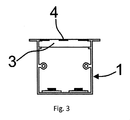
図1から図3を参照すると、検査されることとなる表面の上の、好ましくは、塗装された表面の上の欠陥を検出するための本発明によるデバイスが示されており、そのデバイスは、 Referring to FIGS. 1 to 3, a device according to the invention for detecting defects on a surface to be inspected, preferably on a painted surface, is shown.
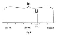
− 検査されることとなる少なくとも1つの表面6、好ましくは、塗装された表面の上に電磁放射線のビームを投射するために、少なくとも1つの第1のスペクトルバンドB1(図4)の中の電磁放射線を放出するように適合されている供給源1と、
-Electromagnetic radiation in at least one first spectral band B1 (FIG. 4) to project a beam of electromagnetic radiation onto at least one
− 少なくとも1つの第2のスペクトルバンドB2(図4)の中において感度の高いビデオカメラ2であって、供給源1によって放出される電磁放射線ビームが投射されるゾーンの中で、検査されることとなる少なくとも1つの表面6のイメージを取得するように配置されている、ビデオカメラ2と、
-A
− 供給源1によって放出される電磁放射線の少なくとも一部を妨害するように適合されており、また、検査されることとなる少なくとも1つの表面6の上の電磁放射線の強度の空間的分布をより均質にするように適合されている、ディフューザー3と
を含む。
-The spatial distribution of the intensity of the electromagnetic radiation on at least one
供給源1は、通常の白熱ランプ、または、ネオンランプもしくはLEDランプ、または、任意の他の供給源、たとえば、レーザーなどであることが可能であり、ビデオカメラが感度の高いスペクトルバンドB2に少なくとも部分的に重なるスペクトルバンドB1の中で放出する。
The
第1のバンドB1と第2のバンドB2との間の交差部は、スペクトルワーキングバンドBLを確立し、スペクトルワーキングバンドBLにおいて、デバイスは、動作する。 The intersection between the first band B1 and the second band B2 establishes a spectral working band BL, in which the device operates.
第1および第2のバンドB1またはB2のうちの一方は、他方の中に完全に含まれ得、それによって、スペクトルワーキングバンドBLは、2つのバンドのうちの一方に対応している。たとえば、図4の例にあるように、ビデオカメラが感度の高い第2のバンドB2は、供給源が放出する第1のバンドB1の中に完全に含まれており、それによって、スペクトルワーキングバンドBLが、ビデオカメラの第2のバンドB2に対応しているということが考えられる。 One of the first and second bands B1 or B2 may be completely contained within the other, whereby the spectral working band BL corresponds to one of the two bands. For example, as in the example of FIG. 4, the second band B2, which is sensitive to the video camera, is completely contained within the first band B1 emitted by the source, thereby the spectral working band. It is conceivable that the BL corresponds to the second band B2 of the video camera.
また、スペクトルワーキングバンドは、いくつかのバンドを含むことが可能であり、たとえば、1つは、可視線の中にあり、1つは、非熱的赤外線の中にある。 Also, the spectral working band can include several bands, for example, one in the visible line and one in the non-thermal infrared.
これは、供給源またはビデオカメラの前に適切なフィルターを配置することによって取得され得る。 This can be obtained by placing an appropriate filter in front of the source or video camera.
ビデオカメラは、300nmから1100nmのスペクトルバンドの中で感度の高いCCD(電荷結合素子)またはCMOS(相補型金属酸化膜半導体)センサーを備えた通常の白黒ビデオカメラを含むことが可能であり、300nmから1100nmのスペクトルバンドは、したがって、非熱的赤外線の一部も含み、それに対して、所望のスペクトルワーキングバンドを選択するために、フィルターが前に置かれる。 The video camera can include a conventional black and white video camera equipped with a CCD (charge coupling element) or CMOS (complementary metal oxide semiconductor) sensor having high sensitivity in the spectrum band of 300 nm to 1100 nm, and can include a 300 nm. The spectral band from 1100 nm also contains some of the non-thermal infrared light, whereas a filter is placed in front to select the desired spectral working band.
そのようなスペクトルワーキングバンドBLが十分に狭い場合には、より良好な結果が取得され得るということが見出された。 It has been found that better results can be obtained if such a spectral working band BL is narrow enough.
この理由のために、スペクトルワーキングバンドは、200nm以下のバンド幅を有しており、また、300nmから1100nmの間にある。 For this reason, the spectral working band has a bandwidth of 200 nm or less and is between 300 nm and 1100 nm.
図3に見ることができるように、ディフューザー3は、供給源1と検査されることとなる表面6との間に間置されるオパリンまたは乳白色の半透明のエレメントを含むことが可能である。通常のランプまたは光供給源は、非均質な強度によって表面を照らすが、放出される電磁放射線の強度が、検査されることとなる表面にわたって均質に分配されているときには、本発明によるデバイスは、より良好な結果を取得する。
As can be seen in FIG. 3, the
これは、検査されることとなる表面から離れるように供給源を移動させることによって取得されるが、電磁放射線の強度は、周知の距離の2乗の法則によって減少する。 This is obtained by moving the source away from the surface to be inspected, but the intensity of electromagnetic radiation is reduced by the well-known square-cube law of distance.
ディフューザー3は、供給源1によって放出される電磁放射線の強度の分布をより均質にすることを助ける。
The
スペクトルワーキングバンドBLが十分に狭くなっており、したがって、50nm以下のバンド幅を有するときには、より良好な結果が取得され、スペクトルワーキングバンドBLが20nm以下のバンド幅を有する場合には、さらにより良好になる。 Better results are obtained when the spectral working band BL is narrow enough and therefore has a bandwidth of 50 nm or less, and even better when the spectral working band BL has a bandwidth of 20 nm or less. become.
また、そのようなスペクトルワーキングバンドBLが非熱的赤外線の中に配置されている場合には、たとえば、スペクトルワーキングバンドBLが750nmから1050nmの間にある場合には、より良好な結果が取得されるということが見出された。 Also, better results are obtained when such a spectral working band BL is located in non-thermal infrared, for example, when the spectral working band BL is between 750 nm and 1050 nm. It was found that
スペクトルワーキングバンドBLが800nmから900nmの間にあり、したがって、可視放射線から十分に遠くにある場合には、さらにより良好になる。 It is even better if the spectral working band BL is between 800 nm and 900 nm and is therefore far enough from visible radiation.
スペクトルワーキングバンドBLが810nmから860nmの間にある場合には、より良好になる。 Better if the spectral working band BL is between 810 nm and 860 nm.
実施された実験に基づいて、最適なものが、2つのスペクトルワーキングバンドBLの中で取得され、第1のものは、825nmから835nmの間にあり、第2のものは、840nmから860nmの間にあるということが見出された。 Based on the experiments carried out, the optimum was obtained in two spectral working bands BL, the first between 825 nm and 835 nm and the second between 840 nm and 860 nm. It was found that it was in.
上述の先行技術から理解されるように、現在存在するデバイスは、多くの場合、検査されることとなる表面の上に複数の明線および暗線を投射し、複数の明線および暗線は、高い光強度および低い光強度を交互にしている。 As can be seen from the prior art described above, currently existing devices often project multiple bright and dark lines onto the surface to be inspected, with the multiple bright and dark lines being high. Alternating light intensity and low light intensity.
線の存在、または、しかし、検査されることとなる表面の上に高強度電磁放射線ゾーンと低強度電磁放射線ゾーンとを交互にする空間的配置の存在は、より良好な結果が取得されることを可能にし、それは、本発明によるデバイスにおいても同様である。 Better results can be obtained with the presence of lines, or the presence of spatial arrangements of alternating high-intensity and low-intensity electromagnetic radiation zones on the surface to be inspected. It is also possible in the device according to the present invention.
この理由のために、本発明によるデバイスは、強度オルタネーター(intensity alternator)4を含み、強度オルタネーター4は、ディフューザー3の後に、供給源1によって放出される電磁放射線を妨害するように適合されており、また、低強度電磁放射線ゾーンと交互になる高強度電磁放射線ゾーンを含む電磁放射線の空間的配置5を、検査されることとなる少なくとも1つの表面6の上に発生させるように適合されている。
For this reason, the devices according to the invention include an
好ましくは(図1Aおよび図1B)、供給源によって放出される電磁放射線の強度分布のそのような空間的配置5は、低強度電磁放射線ラインZ2と交互になる複数の高強度電磁放射線ラインZ1を含み、ラインZ1およびZ2は、実質的に平行になっている。
Preferably (FIGS. 1A and 1B), such a
たとえば、円形同心円状のラインなどのような、他の空間的配置も、当然のことながら可能である。 Other spatial arrangements, such as circular concentric lines, are of course possible.
検査されることとなる表面の上に投射される空間的配置5において、高強度電磁放射線ラインZ1と低強度電磁放射線ラインZ2とを交互にすることは、繰り返しの図を生成させ、そのような繰り返しのピッチP1(図1B)は、好ましくは、小さくなっており、20mm以下になっており、4mm以下である場合には、より良好である。
Alternating high-intensity electromagnetic radiation lines Z1 and low-intensity electromagnetic radiation lines Z2 in a
また、そのようなピッチP1のサイズは、検出されることが望まれる欠陥の最小サイズに依存する。 Also, the size of such pitch P1 depends on the minimum size of defects that are desired to be detected.
当然のことながら、デューティーサイクルは、5%から95%の間で変化するということ、すなわち、高強度電磁放射線ラインZ1の太さは、低強度電磁放射線ラインZ2の太さとは異なるということ、具体的には、高強度電磁放射線ラインZ1の太さは、低強度電磁放射線ラインの太さよりも小さくなっているということが考えられる。 Naturally, the duty cycle varies between 5% and 95%, that is, the thickness of the high intensity electromagnetic radiation line Z1 is different from the thickness of the low intensity electromagnetic radiation line Z2. Therefore, it is considered that the thickness of the high-intensity electromagnetic radiation line Z1 is smaller than the thickness of the low-intensity electromagnetic radiation line.
特定の焦点調節オプティクスも使用することによって、供給源から放出される電磁放射線が十分に拡散され、高強度電磁放射線ゾーンから隣接する低強度電磁放射線ゾーンへの通過が実質的に段階的になるようになっており、高強度電磁放射線ゾーンの中の電磁放射線の強度が均質になるようになっているということが好適である。 By also using specific focusing optics, the electromagnetic radiation emitted from the source is sufficiently diffused so that the passage from the high intensity electromagnetic radiation zone to the adjacent low intensity electromagnetic radiation zone is substantially gradual. It is preferable that the intensity of the electromagnetic radiation in the high-intensity electromagnetic radiation zone is uniform.
図1を参照すると、供給源1によって投射される電磁放射線のビームの中心部分の中で、および、スペクトルワーキングバンドBLの中で、そのような高強度電磁放射線ゾーン(Z1)および低強度電磁放射線ゾーン(Z2)と交差するラインL1の上の電磁放射線強度の分布は、好ましくは、実質的に矩形波の関数になっており、急勾配の立ち上がりエッジおよび立ち下がりエッジ、ならびに、高強度電磁放射線ゾーンZ1の中のおよび低強度電磁放射線ゾーンZ2の中の実質的に均一な値を有しているということが見られ得る。
Referring to FIG. 1, such high-intensity electromagnetic radiation zones (Z1) and low-intensity electromagnetic radiation in the central portion of the beam of electromagnetic radiation projected by
低強度電磁放射線ゾーンZ2および高強度電磁放射線ゾーンZ1の両方の中において、環境照明は、コントラストおよび彩度の減少を生成させることが可能であり、均質に配置されていない場合には、放射強度のより低い均質性を決定することが可能である。 Within both the low-intensity electromagnetic radiation zone Z2 and the high-intensity electromagnetic radiation zone Z1, ambient lighting can produce a reduction in contrast and saturation, and if not uniformly arranged, the radiation intensity. It is possible to determine the lower homogeneity of.
欠陥に対するデバイスのより良好な感度のために、ビデオカメラは、欠陥のない検査されることとなる表面の上に高強度電磁放射線ゾーンZ1を観察するときに、飽和(saturation)に到達しないことが好適である。 Due to the device's better sensitivity to defects, the camcorder may not reach saturation when observing the high intensity electromagnetic radiation zone Z1 over the surface to be inspected without defects. Suitable.
スペクトルワーキングバンドは、2つ以上の異なるスペクトルバンドを含むことが可能であり、イメージ獲得は、スペクトルバンドの上で同時に、または、時間的に連続して(最初に、所定のバンドの上で、次いで、別のバンドの上で)起こることが可能である。 Spectral working bands can include two or more different spectral bands, and image acquisition is simultaneous or temporally continuous over the spectral bands (first, over a given band,). It can then happen (on another band).
異なるバンドの上で取得されるイメージは、信号対雑音比を改善するために、および、検査されることとなる表面の上にある潜在的な欠陥を検出する可能性を増加させるために、好都合な数学的アルゴリズムにしたがって、重ねられるか、または、一緒に処理される。デフレクトメトリー技法に基づくデバイスとは逆に、本発明によるデバイスでは、供給源およびビデオカメラの相対的位置は関係がない。 Images acquired on different bands are useful for improving the signal-to-noise ratio and for increasing the likelihood of detecting potential defects on the surface that will be inspected. They are stacked or processed together according to a mathematical algorithm. Contrary to devices based on the deflationmetry technique, in devices according to the invention, the relative position of the source and the video camera is irrelevant.
図2の表現では、供給源1およびビデオカメラ2は、一緒に近くにあり、相互に拘束されている。
In the representation of FIG. 2, the
ビデオカメラおよび供給源は、好ましくは、検査されることとなる表面に対して垂直の方向に沿って配置されている。そのような配置は、通常、デフレクトメトリー技法の中では採用されない。その理由は、より良好な感度を取得するために、供給源によって放出される電磁放射線が、法線に対して少なくとも45°の角度で、検査されることとなる表面の上に衝突し、一方、ビデオカメラは、電磁放射線の入射方向に対して正反射方向に配置されているということが好適であるからである。 The video camera and source are preferably arranged along a direction perpendicular to the surface to be inspected. Such arrangements are usually not adopted in deflationary techniques. The reason is that in order to obtain better sensitivity, the electromagnetic radiation emitted by the source collides with the surface to be inspected at an angle of at least 45 ° to the normal, while This is because it is preferable that the video camera is arranged in the specular reflection direction with respect to the incident direction of the electromagnetic radiation.
その動作において、供給源1は、低強度電磁放射線ゾーンと交互になる均質な高強度電磁放射線ゾーン(たとえば、ストリップ空間的配置5)を有する電磁放射線のビームを、検査されることとなる表面の上に投射する。
In its operation, the
ビデオカメラ2は、供給源1によって投射されるビームの中心部分の中で、検査されることとなる表面をキャプチャーする。
The
欠陥の存在は、放射強度の均質性を局所的に変更し、または、空間的配置を局所的に変形させ、したがって、欠陥が検出されることを可能にする。たとえば、欠陥は、高強度電磁放射線ゾーンの中に低強度スポットとして出現することが可能であり、および/または、低強度電磁放射線ゾーンの中に高強度スポットとして出現することが可能であり、または、高強度電磁放射線ゾーンと低強度電磁放射線ゾーンとの間の通過が起こるエッジの歪みとして出現することが可能である。 The presence of defects locally alters the homogeneity of radiant intensity or locally deforms the spatial arrangement, thus allowing defects to be detected. For example, defects can appear as low-intensity spots in high-intensity electromagnetic radiation zones and / or can appear as high-intensity spots in low-intensity electromagnetic radiation zones, or , It is possible to manifest as edge distortion resulting in passage between the high intensity electromagnetic radiation zone and the low intensity electromagnetic radiation zone.
好ましくは、検査されることとなる表面は、本発明によるデバイスに対して走っており、検査されることとなる表面の全体のスキャンが迅速に取得され得るようになっている。 Preferably, the surface to be inspected runs against the device according to the invention so that a full scan of the surface to be inspected can be obtained quickly.
イメージ分析のための電子デバイスが、容易におよび自動的に、高い信頼性で欠陥を検出することが可能である。 Electronic devices for image analysis can easily and automatically detect defects with high reliability.
また、本発明は、検査されることとなる表面の上の、好ましくは、塗装された表面の上の欠陥を検出するための方法を保護することを希望しており、方法は、 The present invention also hopes to protect the method for detecting defects on the surface to be inspected, preferably on the painted surface.
a) 少なくとも1つの第1のスペクトルバンドB1の中の電磁放射線を放出するように適合されている電磁放射線供給源1を取得するステップと、
a) The step of acquiring an
b) 検査されることとなる少なくとも1つの表面の上に電磁放射線のビームを投射するステップと、 b) A step of projecting a beam of electromagnetic radiation onto at least one surface to be inspected,
c) 少なくとも1つの第2のスペクトルバンドB2の中において感度の高いビデオカメラ2を取得するステップであって、第1のバンドB1と第2のバンドB2との間の交差部は、ヌルでない(non-null)スペクトルワーキングバンドBLを決定する、ステップと、
c) The step of acquiring a highly
d) 供給源1によって放出される電磁放射線ビームの入射ゾーンの中の検査されることとなる少なくとも1つの表面のイメージを取得するように、ビデオカメラ2を配置するステップと、
d) The step of arranging the
e) ディフューザー3を取得するステップであって、ディフューザー3は、供給源によって放出される電磁放射線の強度の空間的分布をより均質にするように適合されている、ステップと、
e) In the step of acquiring the
f) 供給源1によって放出される電磁放射線の少なくとも一部を妨害するように、および、その強度をより均質にするように、ディフューザー3を配置するステップと、
f) With the step of arranging the
g) 強度オルタネーター4を取得するステップであって、強度オルタネーター4は、高強度電磁放射線ゾーンと低強度電磁放射線ゾーンとを交互にする電磁放射線の空間的配置5を取得するように適合されている、ステップと、
g) In the step of acquiring the
h) ディフューザー3の後に、供給源1によって放出される電磁放射線を妨害するように強度オルタネーター4を配置するステップであって、低強度電磁放射線ゾーンと交互になる高強度電磁放射線ゾーンを、検査されることとなる表面の上に生成させるようになっている、ステップと、
h) After the
i) 検査されることとなる表面にわたる電磁放射線の強度の空間的配置5のイメージを、ビデオカメラから取得するステップと、
i) In the step of acquiring an image of the
j) 高強度電磁放射線ゾーンの中により低い強度スポットを出現させ、および/または、低強度電磁放射線ゾーンの中により高い強度スポットを出現させる欠陥を識別するステップと
を含む。
j) Includes a step of identifying defects that cause lower intensity spots to appear in the high intensity electromagnetic radiation zone and / or higher intensity spots to appear in the low intensity electromagnetic radiation zone.
当然のことながら、方法は、異なるスペクトルワーキングバンドの上でのイメージ獲得、および、数学的アルゴリズムによるイメージの処理を含み、数学的アルゴリズムは、信号対雑音比を増加させるように、および、検査されることとなる表面の上にある可能性のある欠陥を検出する可能性を増加させるように適合されているということが考えられる。 Not surprisingly, the method involves image acquisition on different spectral working bands and processing of the image by a mathematical algorithm, which is tested to increase the signal-to-noise ratio. It is believed that it is adapted to increase the chances of detecting potential defects on the surface that will result in it.
電磁放射線が少なくとも高強度電磁放射線ゾーンの中で均質に分配されているおかげで、塗装欠陥または幾何学的なおよび美観上の欠陥の検出が、他の今日存在するデバイスに対してより容易に行われ、デバイスのより高い信頼性によって、信号対雑音比が改善される。 Detection of paint defects or geometric and aesthetic defects is easier for other today's devices, thanks to the uniform distribution of electromagnetic radiation, at least within the high intensity electromagnetic radiation zone. However, the higher reliability of the device improves the signal-to-noise ratio.
検査は、当然のことながら、人間のオペレーターによって、したがって、ビデオカメラなしに、可視スペクトルの中で行われることが予期され得る。 The inspection can, of course, be expected to be performed by a human operator, and therefore without a video camera, in the visible spectrum.
検査され得る表面は、塗装された表面だけではなく、表面処理(たとえば、樹脂堆積、または、さらには透明なコーティングなど)を施されているかまたは表面処理を施されていない表面でもある。 The surface that can be inspected is not only a painted surface, but also a surface that has or has not been surface treated (eg, resin deposits, or even a clear coating).
また、好適ではないが、本発明によるデバイスは、低強度電磁放射線ゾーンと交互になる高強度電磁放射線ゾーンを有するために、強度オルタネーターを使用するのではなく、検査されることとなる表面にわたって、供給源によって放出される電磁放射線の強度の均質な分布を有するために、単純にディフューザーを使用するということも考えられる。 Also, although not preferred, the devices according to the invention have high intensity electromagnetic radiation zones that alternate with low intensity electromagnetic radiation zones, so rather than using an intensity alternator, over the surface to be inspected. It is also conceivable to simply use a diffuser in order to have a uniform distribution of the intensity of the electromagnetic radiation emitted by the source.
検査されることとなる表面にわたる電磁放射線分布の十分な均質性は、足りていることが多い。 Sufficient homogeneity of the electromagnetic radiation distribution over the surface to be inspected is often sufficient.
本発明の有利な性質は、デフレクトメトリー技法に基づくデバイスとは逆に、本発明によるデバイスがビデオカメラおよび供給源の配置の幅広い自由を可能にするということである。 An advantageous property of the present invention is that the device according to the present invention allows a wide range of freedom in the placement of video cameras and sources, as opposed to devices based on deflectionometry techniques.
Claims (15)
a) 第1のスペクトルバンド(B1)の中の電磁放射線を放出するように適合されている電磁放射線供給源(1)を取得するステップと、
b) 検査されることとなる少なくとも1つの表面(6)の上に電磁放射線のビームを投射するステップと、
c) 第2のスペクトルバンド(B2)の中において感度の高いビデオカメラ(2)を取得するステップであって、前記第1のバンド(B1)と前記第2のバンド(B2)との間の交差部は、ヌルでないスペクトルワーキングバンド(BL)を決定する、ステップと、
d) 前記供給源(1)によって放出される前記電磁放射線ビームの入射ゾーンの中の前記検査されることとなる少なくとも1つの表面(6)のイメージを取得するように、前記ビデオカメラ(2)を配置するステップと
を含む、方法において、
e) ディフューザー(3)が取得され、前記ディフューザー(3)は、前記供給源によって放出される前記電磁放射線の強度の空間的分布をより均質にするように適合されており、
f) 前記ディフューザー(3)は、前記供給源(1)によって放出される前記電磁放射線の少なくとも一部を妨害するように、および、その強度をより均質にするように配置されており、
g) 強度オルタネーター(4)が取得され、前記強度オルタネーター(4)は、高強度電磁放射線ゾーンと低強度電磁放射線ゾーンとを交互にする前記電磁放射線の空間的配置(5)を取得するように適合されており、
h) 前記強度オルタネーター(4)は、前記ディフューザー(3)の後に、前記供給源(1)によって放出される前記電磁放射線を妨害するように配置されており、低強度電磁放射線ゾーンと交互になる高強度電磁放射線ゾーンを、前記検査されることとなる表面(6)の上に生成させるようになっており、
i) 前記検査されることとなる表面の上の前記電磁放射線の前記強度の前記空間的配置(5)のイメージは、前記ビデオカメラから取得され、
j) 前記高強度電磁放射線ゾーンの中により低い強度スポットを出現させ、および/または、前記低強度電磁放射線ゾーンの中により高い強度スポットを出現させる欠陥が、識別されることを特徴とする、方法。 A method for detecting paint defects in painted elements,
a) The step of obtaining an electromagnetic radiation source (1) adapted to emit electromagnetic radiation in the first spectral band (B1), and
b) A step of projecting a beam of electromagnetic radiation onto at least one surface (6) to be inspected,
c) A step of acquiring a highly sensitive video camera (2) in the second spectral band (B2), between the first band (B1) and the second band (B2). The intersection determines the non-null spectral working band (BL), the step and
d) The video camera (2) so as to acquire an image of at least one surface (6) to be inspected in the incident zone of the electromagnetic radiation beam emitted by the source (1). In a method, including steps to place the
e) A diffuser (3) has been acquired and the diffuser (3) is adapted to more homogenize the spatial distribution of the intensity of the electromagnetic radiation emitted by the source.
f) The diffuser (3) is arranged to interfere with at least a portion of the electromagnetic radiation emitted by the source (1) and to make its intensity more homogeneous.
g) The intensity alternator (4) is acquired so that the intensity alternator (4) acquires the spatial arrangement (5) of the electromagnetic radiation that alternates between the high intensity electromagnetic radiation zone and the low intensity electromagnetic radiation zone. It has been adapted and
h) The intensity alternator (4) is arranged after the diffuser (3) so as to interfere with the electromagnetic radiation emitted by the source (1) and alternates with the low intensity electromagnetic radiation zone. A high intensity electromagnetic radiation zone is formed on the surface (6) to be inspected.
i) An image of the spatial arrangement (5) of the intensity of the electromagnetic radiation on the surface to be inspected is obtained from the video camera.
j) A method characterized in that defects that cause lower intensity spots to appear in the high intensity electromagnetic radiation zone and / or higher intensity spots to appear in the low intensity electromagnetic radiation zone are identified. ..
Priority Applications (1)
| Application Number | Priority Date | Filing Date | Title |
|---|---|---|---|
| JP2023084317A JP2023106529A (en) | 2017-07-10 | 2023-05-23 | Device and method for detecting surface defect |
Applications Claiming Priority (3)
| Application Number | Priority Date | Filing Date | Title |
|---|---|---|---|
| IT102017000077459 | 2017-07-10 | ||
| IT102017000077459A IT201700077459A1 (en) | 2017-07-10 | 2017-07-10 | DEVICE AND PROCEDURE FOR DETECTION OF SURFACE DEFECTS |
| PCT/IB2018/055041 WO2019012404A1 (en) | 2017-07-10 | 2018-07-09 | Device and process for detecting surface defects |
Related Child Applications (1)
| Application Number | Title | Priority Date | Filing Date |
|---|---|---|---|
| JP2023084317A Division JP2023106529A (en) | 2017-07-10 | 2023-05-23 | Device and method for detecting surface defect |
Publications (2)
| Publication Number | Publication Date |
|---|---|
| JP2020527728A true JP2020527728A (en) | 2020-09-10 |
| JP2020527728A5 JP2020527728A5 (en) | 2021-07-26 |
Family
ID=61005905
Family Applications (2)
| Application Number | Title | Priority Date | Filing Date |
|---|---|---|---|
| JP2020523065A Pending JP2020527728A (en) | 2017-07-10 | 2018-07-09 | Devices and methods for detecting surface defects |
| JP2023084317A Pending JP2023106529A (en) | 2017-07-10 | 2023-05-23 | Device and method for detecting surface defect |
Family Applications After (1)
| Application Number | Title | Priority Date | Filing Date |
|---|---|---|---|
| JP2023084317A Pending JP2023106529A (en) | 2017-07-10 | 2023-05-23 | Device and method for detecting surface defect |
Country Status (7)
| Country | Link |
|---|---|
| US (2) | US11105614B2 (en) |
| EP (1) | EP3652524B1 (en) |
| JP (2) | JP2020527728A (en) |
| BR (1) | BR112020000286A2 (en) |
| IT (1) | IT201700077459A1 (en) |
| MA (1) | MA49568A (en) |
| WO (1) | WO2019012404A1 (en) |
Families Citing this family (2)
| Publication number | Priority date | Publication date | Assignee | Title |
|---|---|---|---|---|
| IT201700077459A1 (en) * | 2017-07-10 | 2019-01-10 | Tekno Idea Srl | DEVICE AND PROCEDURE FOR DETECTION OF SURFACE DEFECTS |
| CN111189854B (en) * | 2020-04-13 | 2020-08-07 | 征图新视(江苏)科技股份有限公司 | Defect layering detection method of automatic glass cover plate detection system |
Citations (4)
| Publication number | Priority date | Publication date | Assignee | Title |
|---|---|---|---|---|
| WO2008123604A1 (en) * | 2007-03-29 | 2008-10-16 | Toyota Jidosha Kabushiki Kaisha | Surface inspection device |
| US20110181873A1 (en) * | 2008-09-12 | 2011-07-28 | Ceramicam Ltd. | Surface scanning device |
| JP2011232265A (en) * | 2010-04-30 | 2011-11-17 | Honda Motor Co Ltd | Surface inspection device and surface inspection method |
| US20140043602A1 (en) * | 2012-08-07 | 2014-02-13 | Carl Zeiss Industrielle Messtechnik Gmbh | Apparatus and method for inspecting an object |
Family Cites Families (14)
| Publication number | Priority date | Publication date | Assignee | Title |
|---|---|---|---|---|
| US4629319A (en) | 1984-02-14 | 1986-12-16 | Diffracto Ltd. | Panel surface flaw inspection |
| DE4121464A1 (en) * | 1990-06-28 | 1992-01-09 | Mazda Motor | DEVICE FOR DETECTING SURFACE DEFECTS |
| JPH05322543A (en) | 1992-05-22 | 1993-12-07 | Mazda Motor Corp | Surface defect inspection device |
| EP1108197A1 (en) | 1998-09-04 | 2001-06-20 | Siemens Aktiengesellschaft | Device and method for detecting depth and color information of an object to be surveyed |
| DE10110994B4 (en) | 2000-03-09 | 2012-11-29 | Isra Vision Systems Ag | Device for image scanning of an object |
| WO2003016819A1 (en) | 2001-08-14 | 2003-02-27 | Metronom Gmbh Industrial Measurement | Method for measuring surface structures |
| GB0500570D0 (en) * | 2005-01-12 | 2005-02-16 | Enfis Ltd | Sensing in meat products and the like |
| JP5110977B2 (en) * | 2007-06-22 | 2012-12-26 | 株式会社日立ハイテクノロジーズ | Defect observation apparatus and method |
| JP4719284B2 (en) * | 2008-10-10 | 2011-07-06 | トヨタ自動車株式会社 | Surface inspection device |
| US20130057678A1 (en) | 2010-05-17 | 2013-03-07 | Ford Espana S.L. | Inspection system and method of defect detection on specular surfaces |
| EP2799810A1 (en) * | 2013-04-30 | 2014-11-05 | Aimess Services GmbH | Apparatus and method for simultaneous three-dimensional measuring of surfaces with multiple wavelengths |
| WO2017001897A1 (en) * | 2015-06-30 | 2017-01-05 | Bosch Car Multimedia Portugal, S.A. | Device and method for the detection of defects on specular surfaces using diffuse patterned light |
| IT201700077459A1 (en) * | 2017-07-10 | 2019-01-10 | Tekno Idea Srl | DEVICE AND PROCEDURE FOR DETECTION OF SURFACE DEFECTS |
| US11328380B2 (en) * | 2018-10-27 | 2022-05-10 | Gilbert Pinter | Machine vision systems, illumination sources for use in machine vision systems, and components for use in the illumination sources |
-
2017
- 2017-07-10 IT IT102017000077459A patent/IT201700077459A1/en unknown
-
2018
- 2018-07-09 BR BR112020000286-0A patent/BR112020000286A2/en active Search and Examination
- 2018-07-09 US US16/629,530 patent/US11105614B2/en active Active
- 2018-07-09 WO PCT/IB2018/055041 patent/WO2019012404A1/en unknown
- 2018-07-09 EP EP18749871.2A patent/EP3652524B1/en active Active
- 2018-07-09 MA MA049568A patent/MA49568A/en unknown
- 2018-07-09 JP JP2020523065A patent/JP2020527728A/en active Pending
-
2021
- 2021-07-20 US US17/380,285 patent/US11629953B2/en active Active
-
2023
- 2023-05-23 JP JP2023084317A patent/JP2023106529A/en active Pending
Patent Citations (4)
| Publication number | Priority date | Publication date | Assignee | Title |
|---|---|---|---|---|
| WO2008123604A1 (en) * | 2007-03-29 | 2008-10-16 | Toyota Jidosha Kabushiki Kaisha | Surface inspection device |
| US20110181873A1 (en) * | 2008-09-12 | 2011-07-28 | Ceramicam Ltd. | Surface scanning device |
| JP2011232265A (en) * | 2010-04-30 | 2011-11-17 | Honda Motor Co Ltd | Surface inspection device and surface inspection method |
| US20140043602A1 (en) * | 2012-08-07 | 2014-02-13 | Carl Zeiss Industrielle Messtechnik Gmbh | Apparatus and method for inspecting an object |
Also Published As
| Publication number | Publication date |
|---|---|
| US20200173771A1 (en) | 2020-06-04 |
| BR112020000286A2 (en) | 2020-07-14 |
| EP3652524A1 (en) | 2020-05-20 |
| MA49568A (en) | 2020-05-20 |
| WO2019012404A1 (en) | 2019-01-17 |
| US11629953B2 (en) | 2023-04-18 |
| US20210348917A1 (en) | 2021-11-11 |
| EP3652524C0 (en) | 2024-02-14 |
| US11105614B2 (en) | 2021-08-31 |
| IT201700077459A1 (en) | 2019-01-10 |
| EP3652524B1 (en) | 2024-02-14 |
| JP2023106529A (en) | 2023-08-01 |
Similar Documents
| Publication | Publication Date | Title |
|---|---|---|
| JP2023106529A (en) | Device and method for detecting surface defect | |
| US9116134B2 (en) | Inspection apparatus for tubular product and inspection method therefor | |
| JP6229968B2 (en) | Concavity and convexity inspection equipment | |
| JP6834174B2 (en) | Visual inspection method and visual inspection equipment | |
| JP2010532870A (en) | Optical inspection method and inspection apparatus for object surface | |
| US8274053B2 (en) | System and method for valve seat gap evaluation | |
| JP2011512533A (en) | Method for measuring glass surface shape and optical distortion by reflection optical imaging | |
| US20090290781A1 (en) | Illuminating device for cylindrical objects, surface inspection method implemented therewith and computer program product | |
| JP2017120232A (en) | Inspection device | |
| JP5830229B2 (en) | Wafer defect inspection system | |
| JP2011209112A (en) | Appearance inspection method of to-be-inspected object and appearance inspection apparatus of the same | |
| JP6926822B2 (en) | Metal strip surface inspection method and inspection equipment | |
| TW201606288A (en) | Apparatus and method for inspecting substrate | |
| CN105277558B (en) | Multi-step method for studying surface and corresponding equipment | |
| JP2018163134A (en) | Surface inspection method and apparatus for the same | |
| JP4630945B1 (en) | Defect inspection equipment | |
| JP2015200544A (en) | Surface irregularity inspection device and surface irregularity inspection method | |
| Tout et al. | Automatic vision system for wheel surface inspection and monitoring | |
| JP2007205974A (en) | Method of inspecting plating, and method of inspecting lead frame | |
| Blanco et al. | Influence of ambient light on the quality of laser digitized surfaces | |
| US20230419471A1 (en) | Surface inspection system | |
| KR20190002944A (en) | Method for evaluating the soundness of led heat sink by passive infrared thermography | |
| JPH0412255A (en) | Mirror inspecting device | |
| JP6699263B2 (en) | Inspection equipment | |
| JP6358884B2 (en) | Inspection device |
Legal Events
| Date | Code | Title | Description |
|---|---|---|---|
| A521 | Request for written amendment filed |
Free format text: JAPANESE INTERMEDIATE CODE: A523 Effective date: 20200130 |
|
| A521 | Request for written amendment filed |
Free format text: JAPANESE INTERMEDIATE CODE: A523 Effective date: 20210604 |
|
| A621 | Written request for application examination |
Free format text: JAPANESE INTERMEDIATE CODE: A621 Effective date: 20210604 |
|
| A977 | Report on retrieval |
Free format text: JAPANESE INTERMEDIATE CODE: A971007 Effective date: 20220530 |
|
| A131 | Notification of reasons for refusal |
Free format text: JAPANESE INTERMEDIATE CODE: A131 Effective date: 20220621 |
|
| A521 | Request for written amendment filed |
Free format text: JAPANESE INTERMEDIATE CODE: A523 Effective date: 20220921 |
|
| A02 | Decision of refusal |
Free format text: JAPANESE INTERMEDIATE CODE: A02 Effective date: 20230124 |
|
| A521 | Request for written amendment filed |
Free format text: JAPANESE INTERMEDIATE CODE: A821 Effective date: 20230523 |