JP2020508564A - Method and apparatus for bonding substrates - Google Patents
Method and apparatus for bonding substrates Download PDFInfo
- Publication number
- JP2020508564A JP2020508564A JP2019542366A JP2019542366A JP2020508564A JP 2020508564 A JP2020508564 A JP 2020508564A JP 2019542366 A JP2019542366 A JP 2019542366A JP 2019542366 A JP2019542366 A JP 2019542366A JP 2020508564 A JP2020508564 A JP 2020508564A
- Authority
- JP
- Japan
- Prior art keywords
- substrate
- radiation
- amorphous
- substrates
- layers
- Prior art date
- Legal status (The legal status is an assumption and is not a legal conclusion. Google has not performed a legal analysis and makes no representation as to the accuracy of the status listed.)
- Pending
Links
Images

Classifications
-
- H10P10/12—
-
- H10P90/1914—
-
- H10P10/126—
-
- H10P14/3454—
-
- H10P14/6544—
-
- H10P34/00—
-
- H10P34/42—
-
- H10P72/0428—
-
- H10P95/90—
-
- H10W72/076—
Landscapes
- Engineering & Computer Science (AREA)
- Physics & Mathematics (AREA)
- Power Engineering (AREA)
- Condensed Matter Physics & Semiconductors (AREA)
- General Physics & Mathematics (AREA)
- Manufacturing & Machinery (AREA)
- Computer Hardware Design (AREA)
- Microelectronics & Electronic Packaging (AREA)
- High Energy & Nuclear Physics (AREA)
- Chemical & Material Sciences (AREA)
- Crystallography & Structural Chemistry (AREA)
- Health & Medical Sciences (AREA)
- Toxicology (AREA)
- Recrystallisation Techniques (AREA)
- Pressure Welding/Diffusion-Bonding (AREA)
- Electromagnetism (AREA)
- Optics & Photonics (AREA)
- Laminated Bodies (AREA)
Abstract
第1の基板(1,6)を第2の基板(2)に接合する方法が提案されており、この方法は、以下のステップ、すなわち、第1の非晶質層(1a,6a)を第1の基板(1,6)上に形成する、かつ/または第2の非晶質層(2a)を第2の基板(2)上に形成するステップ、第1の基板(1,6)を第2の基板(2)に、1つのまたは複数の非晶質層(1a,2a,6a)で接続し、基板積層体(3)を形成するステップ、1つのまたは複数の非晶質層(1a,2a,6a)が1つのまたは複数の結晶層に転移するように、1つのまたは複数の非晶質層(1a,2a,6a)を、放射(5)により照射するステップ、を有している。There has been proposed a method of bonding the first substrate (1, 6) to the second substrate (2). This method comprises the following steps, namely, the first amorphous layer (1a, 6a) Forming on the first substrate (1,6) and / or forming the second amorphous layer (2a) on the second substrate (2), the first substrate (1,6) Is connected to the second substrate (2) by one or more amorphous layers (1a, 2a, 6a) to form a substrate stack (3), one or more amorphous layers Irradiating one or more amorphous layers (1a, 2a, 6a) with radiation (5) such that (1a, 2a, 6a) is transformed into one or more crystal layers. doing.
Description
本発明は、独立請求項に記載の基板を接合する方法ならびに装置、ならびに基板積層体に関する。半導体産業では数年来既に、基板を互いに接合させるために様々な接合技術が使用されている。接合工程はボンディングと呼ばれる。特に、仮接合法と永久接合法とは異なるものである。 The present invention relates to a method and an apparatus for bonding substrates as described in the independent claims, and to a substrate stack. Various bonding techniques have been used in the semiconductor industry for several years to bond substrates together. The joining process is called bonding. In particular, the temporary joining method and the permanent joining method are different.
仮接合法では、特に製品基板が支持基板に貼り合わせられ、所定のプロセス後に再びこの支持基板を剥がすことができる。仮接合法により、製品基板は機械的に安定化され得る。機械的安定化により、アーチ状になったり、変形したり、または破損したりすることなく製品基板を取り扱うことができる。支持基板による安定化はとりわけ、裏面薄化プロセス中および裏面薄化プロセス後に必要である。裏面薄化プロセスにより、製品基板の厚さを数マイクロメートルにまで減じることができる。 In the temporary joining method, in particular, a product substrate is bonded to a support substrate, and the support substrate can be peeled off again after a predetermined process. The product substrate can be mechanically stabilized by the temporary bonding method. The mechanical stabilization allows the product substrate to be handled without arching, deformation, or breakage. Stabilization by the support substrate is necessary, inter alia, during and after the backside thinning process. The backside thinning process can reduce the thickness of the product substrate to a few micrometers.
永久接合法では、少なくとも2つの基板が継続的に、永久的に互いに接合される。2つの基板の永久接合により、多層の構造体の製造も可能である。この多層の構造体は、同じまたは異なる材料から成っていてよい。 In the permanent bonding method, at least two substrates are continuously and permanently bonded to each other. Due to the permanent bonding of the two substrates, the production of multilayer structures is also possible. The multilayer structure may be made of the same or different materials.
陽極接合による永久接合法は、イオンを含む基板を永久的に互いに接続するために使用される。多くの場合、両基板の一方はガラス基板である。 Permanent bonding by anodic bonding is used to permanently connect substrates containing ions to each other. In many cases, one of the two substrates is a glass substrate.
別の永久接合法は金属接合である。金属接合では、接合すべき基板間に合金が形成される、またはホモ原子結合、すなわち1種類の原子のみから成る結合が行われる。可能な硬化工程では、液相が硬化して、両基板間に結合層が形成される。溶融相の形成なしに行われる結合も考えられる。 Another permanent joining method is metal joining. In metal bonding, an alloy is formed between the substrates to be bonded, or a homoatomic bond, ie, a bond consisting of only one type of atom, is made. In a possible curing step, the liquid phase is cured to form a tie layer between the two substrates. Bonding that takes place without the formation of a molten phase is also conceivable.
別の永久接合法は、直接接合とも言われるフュージョンボンディングである。フュージョンボンディングでは、2つの平坦な純粋な基板表面が、接触させられることにより互いに接合される。この場合、接合工程は2つのステップに分割される。第1のステップでは、両基板の接触が行われる。この場合、両基板の固定は主に、ファン・デル・ヴァールス力によって行われる。この固定は予備接合(英語:prebond)と呼ばれる。ファン・デル・ヴァールス力により、特に剪断力をかけることによっては、著しい力をかけてしか、基板を相互に摺動させることができないほどしっかりと基板を互いに接合させる、十分強力な固定を形成することができる。一方、両基板は、特に法線力を加えることによって再び互いに容易に分離させることができる。この場合、法線力は好適には縁部に作用し、両基板の境界面にくさび効果を生じさせ、このくさび硬化により、連続した亀裂を発生させ、これにより両基板を再び互いに分離させる。永久フュージョンボンディングを形成するために、基板積層体に、アニーリングとも呼ばれる熱処理を施す。この熱処理により、両基板の表面間に共有結合が形成される。このように形成された永久接合は、多くの場合、基板の破壊を伴う相応に高い力をかけてしか解消することはできない。 Another permanent bonding method is fusion bonding, also called direct bonding. In fusion bonding, two flat, pure substrate surfaces are joined together by contact. In this case, the joining process is divided into two steps. In the first step, the two substrates are brought into contact. In this case, the fixing of both substrates is mainly performed by the van der Waals force. This fixation is called prebonding. By van der Waals forces, especially by applying shear forces, form a sufficiently strong anchor that bonds the substrates together so tightly that the substrates cannot slide relative to each other only with significant force be able to. On the other hand, both substrates can be easily separated from each other again, especially by applying a normal force. In this case, the normal force preferably acts on the edge, creating a wedge effect at the interface between the two substrates, which hardening causes continuous cracking, thereby causing the two substrates to separate again from each other. In order to form permanent fusion bonding, the substrate laminate is subjected to a heat treatment, also called annealing. By this heat treatment, a covalent bond is formed between the surfaces of both substrates. The permanent bond formed in this way can often only be eliminated with a correspondingly high force with a destruction of the substrate.
接合強度を得るために必要な熱処理も、技術的な課題を含む。接合される基板の多くには既に、機能的なユニット、例えばマイクロチップ、MEMS、センサ、LEDが設けられおり、これらは熱に敏感である。特にマイクロチップは比較的高度にドープされている。ドープ要素は、高温では、高い拡散能力を有し、これにより基板においてドーピングの望ましくない欠点となる分散が生じる恐れがある。さらに、熱処理は常に、高い温度、ひいては高いコストを伴い、熱的応力の発生、熱的に条件付けられた摺動、加熱と冷却のための比較的長い工程時間を伴う。したがって、できるだけ低い温度で接合されるのが望ましい。 The heat treatment required to obtain the bonding strength also involves technical issues. Many of the substrates to be bonded are already provided with functional units, such as microchips, MEMS, sensors, LEDs, which are sensitive to heat. In particular, microtips are relatively highly doped. At high temperatures, the doped elements have a high diffusion capacity, which can result in dispersion in the substrate, which is an undesirable disadvantage of doping. Furthermore, heat treatment always involves high temperatures and thus high costs, and involves relatively long process times for the generation of thermal stresses, thermally conditioned sliding, heating and cooling. Therefore, it is desirable that the bonding be performed at a temperature as low as possible.
直接接合のさらなる方法は、表面活性化された直接接合である。基板のうちの少なくとも1つを表面活性化することにより、接合の表面エネルギは高められるので、基板材料の強度に匹敵する接合強度が、室温で生じる。 A further method of direct bonding is surface activated direct bonding. By surface activating at least one of the substrates, the surface energy of the bond is increased, so that a bond strength comparable to that of the substrate material occurs at room temperature.
表面処理温度もしくは期間を減じることができる表面活性化のために、様々なアプローチがある。接合すべき表面の処理のために、プラズマ処理またはイオンビーム処理を使用することができる。本発明によれば、全てではないが殆どの表面活性化法は、接合すべき表面の非晶質化を伴う。 There are various approaches for surface activation that can reduce the surface treatment temperature or duration. For treatment of the surfaces to be joined, plasma treatment or ion beam treatment can be used. According to the invention, most, if not all, surface activation methods involve amorphization of the surface to be joined.
基板表面の清浄化および活性化のためのプラズマ処理によれば、比較的低温での接合が可能である。しかしながらこのようなプラズマ法は、酸素親和性の表面、特に金属表面では機能しない、または極めて限定的にしか機能しない。酸素親和性の金属は酸化し、一般的に比較的安定的な酸化物を形成する。酸化物も接合工程には障害となる。このように酸化された金属は、拡散接合により互いに接続することも比較的困難であり得る。これに対し、二酸化ケイ素層を形成する、プラズマにより活性化された特に単結晶のシリコンの接合は極めて良好に機能する。二酸化ケイ素層は接合に極めて適している。したがって、酸化物の上述したネガティブな作用は、必ずしも全ての材料クラスに関するものではない。 According to the plasma treatment for cleaning and activating the substrate surface, bonding at a relatively low temperature is possible. However, such a plasma method does not work, or only very poorly, on oxygen affinity surfaces, especially metal surfaces. Oxygen affinity metals oxidize and generally form relatively stable oxides. Oxides also hinder the bonding process. Such oxidized metals can also be relatively difficult to connect to each other by diffusion bonding. In contrast, the bonding of plasma-activated, especially single-crystal silicon, which forms the silicon dioxide layer, works very well. Silicon dioxide layers are very suitable for bonding. Therefore, the above-mentioned negative effects of oxides do not necessarily relate to all material classes.
刊行物である米国特許第5441776号明細書には、一次電極を、水素化非晶質ケイ素層に結合する方法が開示されている。この非晶質ケイ素層は、堆積プロセスにより基板の表面に堆積される。 Publication US Pat. No. 5,441,776 discloses a method of bonding a primary electrode to a hydrogenated amorphous silicon layer. This amorphous silicon layer is deposited on the surface of the substrate by a deposition process.
刊行物である米国特許第7462552号明細書には、非晶質シリコン層を基板の表面に堆積させるために、化学気相成長(英語:chemical vapour deposition, CVD)を使用する方法が示されている。非晶質層は0.5〜10μmの厚さを有している。 The publication US Pat. No. 7,462,552 shows a method of using chemical vapor deposition (CVD) to deposit an amorphous silicon layer on the surface of a substrate. I have. The amorphous layer has a thickness of 0.5 to 10 μm.
文献には、低温での直接接合を説明した様々なアプローチがある。PCTの欧州特許出願公開第2013/064239号明細書のアプローチでは、接合プロセス中および/または接合プロセス後に、基板材料において溶解する犠牲層が設けられている。PCTの欧州特許出願公開第2011/064874号明細書における別のアプローチでは、相転移による永久接続の形成が記載されている。上記文献は、特に金属表面に関するものであって、金属表面は、共有結合を介してではなく、金属結合を介して結合される。PCTの欧州特許出願公開第2014/056545号明細書には、表面清浄化によるシリコンの最適化された直接接合工程について記載されている。 There are various approaches in the literature that describe direct bonding at low temperatures. In the approach of PCT publication EP 2013/064239, a sacrificial layer is provided that dissolves in the substrate material during and / or after the bonding process. Another approach in PCT publication 2011/064874 describes the formation of a permanent connection by phase transition. The above-mentioned documents relate in particular to metal surfaces, which are bonded not via covalent bonds but via metal bonds. PCT European Patent Application Publication No. 2014/056545 describes an optimized direct bonding process of silicon by surface cleaning.
別のアプローチは国際公開第2015197112号に開示されており、この場合、上述した技術の多くの欠点が減じられている。これにより、接合層は、数10nmの薄さに保持されるので、積層体の好適な特性が特に僅かに影響を受ける。 Another approach is disclosed in WO2015197112, in which many of the disadvantages of the techniques described above are reduced. As a result, the bonding layer is kept at a thickness of a few tens of nanometers, so that the favorable properties of the laminate are particularly slightly affected.
刊行物である米国特許出願公開第20130112650号明細書ならびに米国特許出願公開第20140230990号明細書は、一種の溶接接合を示しており、この場合、接合すべき表面に、レーザービームにより局所的に溶融される金属層が塗布される。これにより、基板を接合することができる少なくとも線状の接合部が生じる。 The publications U.S. Patent Application Publication No. 20130112650 and U.S. Patent Application Publication No. 20140230990 describe a type of welded joint where the surface to be joined is locally melted by a laser beam. The metal layer to be applied is applied. As a result, at least a linear bonding portion that can bond the substrates is generated.
上述した全ての方法ならびに接合装置は、接合方法により、接合された基板積層体を形成する。しかしながら、全ての方法では、金属および/またはそのイオンのような添加材料が使用される、または基板の酸化物および/または窒化物が形成されて、互いに接続される。 All of the above-described methods and bonding apparatuses form a bonded substrate laminate by a bonding method. However, in all methods, additional materials such as metals and / or their ions are used, or oxides and / or nitrides of the substrate are formed and connected to each other.
したがって、本発明の課題は、従来技術の欠点を解消し、特に改善された接合結果を提供することである。 It is therefore an object of the present invention to overcome the disadvantages of the prior art and to provide particularly improved joining results.
この課題は、独立請求項の対象により解決される。本発明の好適な別の構成は従属請求項に記載されている。明細書、請求の範囲、および/または図面に記載された少なくとも2つの特徴から成る全ての組み合わせも本発明の範囲である。数値範囲においては、上記範囲内にある値も、限界値として開示されたものとみなされ、任意の組み合わせで特許請求することができる。 This problem is solved by the subject matter of the independent claims. Further advantageous embodiments of the invention are described in the dependent claims. All combinations of at least two features described in the description, claims, and / or drawings are also within the scope of the present invention. In the numerical ranges, values within the above ranges are also considered to be disclosed as limiting and may be claimed in any combination.
本発明によれば、第1の基板を第2の基板に接合する方法であって、
第1の非晶質層を第1の基板上に形成する、かつ/または第2の非晶質層を第2の基板上に形成するステップと、
第1の基板を第2の基板に、1つのまたは複数の非晶質層で接続し、基板積層体を形成するステップと、
1つのまたは複数の非晶質層を、1つのまたは複数の非晶質層が、1つのまたは複数の結晶層に転移するように、放射により照射するステップと、
を有している方法が提供される。
According to the present invention, there is provided a method of bonding a first substrate to a second substrate,
Forming a first amorphous layer on a first substrate and / or forming a second amorphous layer on a second substrate;
Connecting the first substrate to the second substrate with one or more amorphous layers to form a substrate stack;
Irradiating the one or more amorphous layers with radiation such that the one or more amorphous layers transform into one or more crystalline layers;
Are provided.
さらに本発明によれば、特に本発明による方法により第1の基板を第2の基板に接合する装置であって、
基板を保持するための保持装置と、
基板を接合するための接合装置と、
照射装置と、
を有しており、
第1の非晶質層を第1の基板上に形成可能であり、かつ/または第2の非晶質層を第2の基板上に形成可能であり、
第1の基板を第2の基板に、1つのまたは複数の非晶質層で接続して、基板積層体を形成可能であり、
1つのまたは複数の非晶質層を、1つのまたは複数の非晶質層が、1つのまたは複数の結晶層に転移可能であるように、放射装置により放射を照射可能であるように、形成されている、
装置が提供される。
Further according to the present invention is an apparatus for joining a first substrate to a second substrate, particularly by the method according to the present invention,
A holding device for holding the substrate,
A joining device for joining the substrates,
An irradiation device;
Has,
A first amorphous layer can be formed on a first substrate, and / or a second amorphous layer can be formed on a second substrate;
Connecting the first substrate to the second substrate with one or more amorphous layers to form a substrate stack;
Forming one or more amorphous layers such that one or more amorphous layers can be transferred to one or more crystalline layers, and can be irradiated with radiation by a radiation device. Have been
An apparatus is provided.
さらに本発明によれば、本発明による装置および/または本発明による方法を用いて接合された、基板積層体が提供される。 Further according to the invention, there is provided a substrate stack joined using the device according to the invention and / or the method according to the invention.
本発明によれば、個々の2つの基板を互いに接合することができる。しかしながら、1つの基板を1つの基板積層体に接合することもでき、または2つの基板積層体を互いに接合することもできる。基板積層体は、2つ以上の接合された基板から成る。 According to the present invention, two individual substrates can be bonded to each other. However, one substrate can be joined to one substrate stack, or two substrate stacks can be joined to each other. The substrate stack consists of two or more bonded substrates.
接合すべき基板もしくは基板積層体は、片面にのみ非晶質層を有していてよく、または両面に非晶質層を有していてもよい。 The substrate or substrate laminate to be bonded may have an amorphous layer only on one side, or may have an amorphous layer on both sides.
簡略化のために以下の記載では、特に規定されない場合は、基板とは、個々の基板も基板積層体も意味する。 In the following description for simplicity, unless otherwise specified, the term “substrate” means both an individual substrate and a substrate laminate.
本発明の根底にある思想は、少なくとも1つの非晶質層により、基板の良好な予備固定(予備接合)が形成され、非晶質層を結晶相に転移させることにより、ほぼ遷移なく接合された基板積層体が形成されるというものである。本発明によれば、発生する熱は、レーザーの波長を正しく選択することにより比較的僅かであり、非晶質層上へと局所的に制限される。したがって基板積層体内の応力を極めて僅かにすることができる。さらにプロセス時間も比較的僅かである。 The idea underlying the invention is that at least one amorphous layer forms a good pre-fixation of the substrate (pre-junction) and the transition of the amorphous layer to the crystalline phase results in a substantially transition-free junction. A substrate laminate is formed. According to the invention, the heat generated is relatively small by the correct choice of the wavelength of the laser and is locally restricted on the amorphous layer. Therefore, the stress in the substrate laminate can be made extremely small. Furthermore, the process time is relatively short.
少なくとも1つの非晶質層が、基板表面の少なくとも部分領域で形成されるので、予備接合が達成可能である。好適には、少なくとも1つの非晶質層は、基板表面全体に形成され、これにより予備接合は最大強度で達成可能である。しかしながら、特にハイブリッド接合の導電性表面領域の場合には、非晶質層は基板表面の部分領域にのみ形成されてもよい。 Pre-bonding is achievable because at least one amorphous layer is formed in at least a partial region of the substrate surface. Preferably, at least one amorphous layer is formed over the entire surface of the substrate, so that pre-bonding can be achieved with maximum strength. However, especially in the case of the conductive surface region of the hybrid junction, the amorphous layer may be formed only in a partial region of the substrate surface.
非晶質層の照射中に、特に、ファン・デル・ヴァールス力により生じる基板の接合は、強固な、特に原子間の接合に、特に共有結合に変換され、存在している欠陥は閉じられる。 During the irradiation of the amorphous layer, in particular, the bonding of the substrate caused by van der Waals forces is converted into strong, especially interatomic, in particular covalent bonds, and the existing defects are closed.
本発明によれば、基板のうちの少なくとも1つは、非晶質層によってカバーされている。基板のうちの1つのみが非晶質層によってカバーされていて、他の基板は非晶質層によってカバーされていない場合、基板は互いに非晶質層で接合される。 According to the invention, at least one of the substrates is covered by an amorphous layer. If only one of the substrates is covered by the amorphous layer and the other substrate is not covered by the amorphous layer, the substrates are joined to each other by the amorphous layer.
好適には、両基板上に非晶質層が形成され、両基板は非晶質層で互いに接続される。これにより好適には特に堅固な予備接合を形成することができる。 Preferably, an amorphous layer is formed on both substrates, and both substrates are connected to each other by the amorphous layer. This advantageously makes it possible to form a particularly strong prebond.
好適には、基板のうちの少なくとも一方が結晶基板、特に単結晶基板である。極めて好適には、基板の両方が結晶基板、特に単結晶基板である。これにより好適には、放射が非晶質層にほぼ妨げられることなく到達することができ、これにより基板の加熱が最小にされ、これにより基板積層体における応力を最小にすることができる。基板が多結晶、特にナノ結晶であることも考えられる。特に当業者には公知のハイブリッド接合の場合、互いに接続すべき導電領域は、好適には多結晶から成り、特に多結晶銅から成る。本発明による方法は、このような場合、必要であれば、基板の部分領域でのみ使用されてもよく、必ずしも基板の領域全体で行う必要はない。しかしながら、特にハイブリッド表面は同時に非晶質化することができるので、ハイブリッド表面の全ての誘電的および電気的領域の全面的な非晶質化は、特に好適である。 Preferably, at least one of the substrates is a crystalline substrate, especially a single crystalline substrate. Very preferably, both substrates are crystalline substrates, especially single crystalline substrates. This preferably allows radiation to reach the amorphous layer almost unhindered, thereby minimizing heating of the substrate and thereby minimizing stress in the substrate stack. It is also conceivable that the substrate is polycrystalline, in particular nanocrystalline. Particularly in the case of hybrid junctions known to those skilled in the art, the conductive regions to be connected to one another preferably consist of polycrystalline, in particular of polycrystalline copper. The method according to the invention may in such cases be used only in partial areas of the substrate, if necessary, and not necessarily in the entire area of the substrate. However, complete amorphization of all dielectric and electrical regions of the hybrid surface is particularly preferred, especially since the hybrid surface can be simultaneously amorphized.
本発明によれば、少なくとも1つの非晶質層は、少なくとも所定の領域で、結晶層に転移するので、ほぼ遷移のない基板積層体が形成される。好適には、少なくとも1つの非晶質層は大部分、極めて特に好適には完全に1つの結晶層に転移する。これにより好適には、殆ど完全に遷移のない、もしくは完全に遷移のない基板積層体を形成することができる。 According to the present invention, at least one amorphous layer is transformed into a crystal layer at least in a predetermined region, so that a substrate laminate having almost no transition is formed. Preferably, the at least one amorphous layer transforms largely, very particularly preferably completely, into one crystalline layer. This makes it possible to preferably form a substrate laminate almost completely free of transition or completely free of transition.
本発明によれば、1つのまたは複数の基板の接合すべき表面(以下では接合表面とも言う)の少なくとも部分領域に非晶質層を形成する。好適には、1つのまたは複数の基板の接合表面の大部分に非晶質層が形成される。特に好適には、1つのまたは複数の基板の接合表面全体に非晶質層が形成される。これにより好適には、特に堅固な予備接合を形成することができ、かつ殆ど遷移のないもしくは完全に遷移のない基板積層体を形成することができる。 According to the present invention, an amorphous layer is formed on at least a partial region of one or more substrates to be bonded (hereinafter also referred to as a bonding surface). Preferably, the amorphous layer is formed on most of the bonding surface of the one or more substrates. Particularly preferably, an amorphous layer is formed over the entire bonding surface of one or more substrates. This advantageously makes it possible to form particularly rigid prebonds and to form a substrate stack with little or no transition.
好適にはさらに、第1の基板および/または第2の基板の結晶相は、使用される放射源の放射に対して、少なくとも50%、好適には少なくとも70%、さらに好適には少なくとも90%、極めて好適には少なくとも95%、最も好適には少なくとも99%透過性である。これにより、放射はほぼ妨げられずに非晶質層へと到達することができるので、基板を透過しての非晶質層の転移が可能である。これにより好適には、1つのまたは複数の非晶質層全体に放射が到達することができる。さらに好適には、放射の放射源を基板の背面に配置することができる。背面とは、基板の、接合表面に面していない側である。 Preferably further, the crystalline phase of the first substrate and / or the second substrate is at least 50%, preferably at least 70%, more preferably at least 90% with respect to the radiation of the radiation source used. Very preferably at least 95%, most preferably at least 99% permeable. As a result, the radiation can reach the amorphous layer almost unhindered, and the transition of the amorphous layer through the substrate is possible. This preferably allows the radiation to reach the entire amorphous layer or layers. More preferably, the radiation source of the radiation can be arranged on the back of the substrate. The back side is the side of the substrate not facing the bonding surface.
本発明によれば、少なくとも1つの非晶質層が放射を少なくとも部分的に吸収する。好適には、放射の放射エネルギの50%超が、さらに好適には70%超が、特に好適には80%超が、極めて特に好適には90%超が、吸収される。これにより好適には特に効果的な結晶相への転移が行われ得る。 According to the invention, at least one amorphous layer at least partially absorbs the radiation. Preferably, more than 50%, more preferably more than 70%, particularly preferably more than 80%, very particularly preferably more than 90% of the radiant energy of the radiation is absorbed. This advantageously allows a particularly effective transformation to the crystalline phase to take place.
好適には放射はレーザー放射である。レーザー放射は少なくとも1つの非晶質層へと収束され、したがって少なくとも1つの非晶質層にのみ作用する。これにより好適には、基板積層体の熱的負荷、ひいては誘導される機械的応力が減じられる。 Preferably the radiation is laser radiation. The laser radiation is focused on at least one amorphous layer and thus acts only on at least one amorphous layer. This advantageously reduces the thermal loading of the substrate stack and thus the induced mechanical stress.
好適にはさらに、放射は、非晶質層に垂直に当てられる。垂直とは、垂直の角度から±5度未満の、好適には±3度未満の、好適には±1度未満のずれを含む。これにより、放射を少なくとも1つの非晶質層によって最適に吸収することができるので、特に効果的な結晶相への転移を達成可能である。さらに、照射を、1つのまたは複数の基板の背面から行うことができ、これにより1つのもしくは複数の非晶質層全体に放射が到達することができる。 さらに、側方からの照射は必要ないので、放射源および基板の配置を簡略化することができる。 Preferably further, the radiation is directed perpendicular to the amorphous layer. Vertical includes a deviation of less than ± 5 degrees, preferably less than ± 3 degrees, and preferably less than ± 1 degree from a vertical angle. This makes it possible to achieve a particularly effective transition to the crystalline phase, since the radiation can be optimally absorbed by the at least one amorphous layer. Furthermore, the irradiation can be performed from the back of the one or more substrates, so that the radiation can reach the entire one or more amorphous layers. Further, since irradiation from the side is not required, the arrangement of the radiation source and the substrate can be simplified.
好適にはさらに、1eV〜10E6eVの、好適には1eV〜10E3eVの、さらに好適には1eV〜10eVの、最も好適には1eV〜3eVのエネルギ範囲で放射する広帯域エミッタによって、放射を発生させる。好適には、このエネルギ範囲の放射は、1つのまたは複数の基板によってほぼ妨げられずに透過され、1つのまたは複数の非晶質層によって吸収されるので、結晶相への転移が行われ得る。これにより、1つのもしくは複数の非晶質層全体に到達することができ、1つのもしくは複数の基板の背面から照射を行うことができる。 Preferably, the radiation is further generated by a broadband emitter emitting in the energy range of 1 eV to 10E6 eV, preferably 1 eV to 10E3 eV, more preferably 1 eV to 10 eV, most preferably 1 eV to 3 eV. Preferably, radiation in this energy range is transmitted substantially unhindered by one or more substrates and is absorbed by one or more amorphous layers, so that a transition to a crystalline phase can occur. . Thereby, one or a plurality of amorphous layers can be entirely reached, and irradiation can be performed from the back surface of one or a plurality of substrates.
好適にはさらに、放射の放射出力は、0.01ワット〜10000ワットであって、好適には0.1ワット〜1000ワットであって、最も好適には1ワット〜100ワットである。この出力範囲では、少なくとも1つの非晶質層を最適温度にもたらすことができるので、結晶相への転移が行われ得る。 Preferably further, the radiation output of the radiation is between 0.01 Watt and 10000 Watt, preferably between 0.1 Watt and 1000 Watt, most preferably between 1 Watt and 100 Watt. In this power range, at least one amorphous layer can be brought to an optimum temperature, so that a transition to a crystalline phase can take place.
好適にはさらに、放射により、1つのまたは複数の非晶質層に、200℃超の、好適には400℃超の、特に好適には600℃超の、さらに好適には800℃超の、最も好適には1200℃超の温度を発生させる。この温度範囲では、特に効果的な結晶相への転移が行われ得る。 Preferably furthermore, the radiation causes the one or more amorphous layers to have a temperature of more than 200 ° C., preferably more than 400 ° C., particularly preferably more than 600 ° C., more preferably more than 800 ° C. Most preferably, temperatures above 1200 ° C are generated. In this temperature range, a particularly effective transformation to the crystalline phase can take place.
好適にはさらに、1点への入射時間は、30秒未満であり、好適には15秒未満であり、特に好適には1秒未満であり、極めて特に好適には100ミリ秒未満である。非晶質層のみが照射されるので、この時間範囲内で結晶相への転移を達成することができ、これによりプロセス時間の著しい短縮が達成可能である。 Preferably, furthermore, the time of incidence at one point is less than 30 seconds, preferably less than 15 seconds, particularly preferably less than 1 second and very particularly preferably less than 100 milliseconds. Since only the amorphous layer is irradiated, a transition to the crystalline phase can be achieved within this time range, whereby a significant reduction in the processing time can be achieved.
好適にはさらに、基板面および/または基板積層体面での放射の反射は、放射源の出力強度の4%未満であり、好適には3%未満であり、特に好適には1%未満である。これにより、1つのまたは複数の基板への放射の入射の際のエネルギ損失が最小にされるので、非晶質層の結晶相への転移のために最大限のエネルギを利用することができる。 Preferably furthermore, the reflection of the radiation at the substrate surface and / or at the substrate stack surface is less than 4%, preferably less than 3%, particularly preferably less than 1% of the output intensity of the radiation source. . This minimizes the energy loss when the radiation is incident on one or more substrates, so that the maximum energy can be used for the transition of the amorphous layer to the crystalline phase.
特に、少なくとも1つの反射防止層および/または少なくとも1つのモスアイ構造が、1つもしくは複数の基板の、接合表面とは反対側に位置する側に設けられ、この場合、特に液体および/または液体膜が放射源と基板表面との間に配置される。 In particular, at least one anti-reflection layer and / or at least one moth-eye structure are provided on one or more substrates on the side opposite the bonding surface, in particular liquid and / or liquid films Is located between the radiation source and the substrate surface.
透過性、すなわち放射が入射する表面での光の強度と、本発明による非晶質接合境界面における光の強度との間の比は、ランベルト・ベールの法則により、材料を通る透過経路の長さおよび材料の吸収率に依存する。材料の吸収率は、波長の関数である。したがって、上記透過率値は、本発明によれば、所与の厚さおよび波長でそれぞれ使用される材料の結晶相を透過するできるだけ高い透過率が求められるという意味で、好適には全ての材料/厚さ/波長の組み合わせに適用される。 The transmission, i.e. the ratio between the light intensity at the surface where the radiation is incident and the light intensity at the amorphous junction interface according to the invention, depends on the Lambert-Beer law, the length of the transmission path through the material. And the absorption of the material. The absorption of a material is a function of wavelength. Thus, the transmittance values are preferably determined according to the present invention in the sense that as high a transmission as possible through the crystalline phase of the material used at a given thickness and wavelength is required, for all materials Applies to the / thickness / wavelength combination.
これにより、1つのまたは複数の基板を放射が通過する際のエネルギ損失が最小にされるので、非晶質層の結晶相への転移のために最大限のエネルギを利用することができる。 This minimizes the energy loss as radiation passes through one or more substrates, so that the maximum energy can be used for the transition of the amorphous layer to the crystalline phase.
この場合、放射の波長に依存した透過率の変動は10%未満であり、好適には5%未満であり、特に好適には3%未満であり、極めて特に好適には1%未満である。 In this case, the variation of the transmission as a function of the wavelength of the radiation is less than 10%, preferably less than 5%, particularly preferably less than 3% and very particularly preferably less than 1%.
好適にはさらに、照射前および/または照射中、基板のうちの少なくとも1つの基板の、好適には両方の基板の加熱を行い、この場合、1つのまたは複数の基板を、25℃を超えるように、好適には150℃を超えるように、特に好適には300℃を超えるように加熱する。加熱により好適には、少なくとも1つの非晶質層の結晶相への転移を促進することができ、容易にすることができる。 Preferably, furthermore, before and / or during the irradiation, heating of at least one of the substrates, preferably both, is performed, wherein the one or more substrates are heated to above 25 ° C. Preferably, it is heated to above 150 ° C, particularly preferably above 300 ° C. Heating can preferably facilitate and facilitate the transition of at least one amorphous layer to a crystalline phase.
好適にはさらに、非晶質層を、非晶質化法によって、特にイオンビーム法および/またはプラズマ法によって形成することができ、この場合、1つのまたは複数の基板に当たる粒子は、0.01eV〜1000eVの、好適には0.1eV〜100eVの、さらに好適には1eV〜10eVのエネルギを有している。 Preferably, furthermore, the amorphous layer can be formed by an amorphization method, in particular by an ion beam method and / or a plasma method, wherein the particles hitting one or more substrates have a particle size of 0.01 eV. It has an energy of 10001000 eV, preferably 0.1 eV-100 eV, more preferably 1 eV-10 eV.
基板への粒子の進入深さは、この場合、0nmよりも大きく、好適には5nmよりも大きく、さらに好適には10nmよりも大きく、極めて好適には25nmよりも大きく、最も好適には50nmよりも大きい。 The penetration depth of the particles into the substrate is in this case greater than 0 nm, preferably greater than 5 nm, more preferably greater than 10 nm, very preferably greater than 25 nm, most preferably greater than 50 nm. Is also big.
好適には、非晶質層の厚さは、50nm未満であり、好適には20nm未満であり、特に好適には10nm未満であり、極めて特に好適には5nm未満であり、最適には2nm未満であり、理想的には1nm未満である。したがって好適には、遷移のない基板積層体を形成することができる。 Preferably, the thickness of the amorphous layer is less than 50 nm, preferably less than 20 nm, particularly preferably less than 10 nm, very particularly preferably less than 5 nm and optimally less than 2 nm. And ideally less than 1 nm. Therefore, it is possible to preferably form a transition-free substrate laminate.
好適には、非晶質層の層厚さのばらつきは、基板結晶の格子定数の20倍未満であり、好適には基板結晶の格子定数の10倍未満であり、特に好適には基板結晶の格子定数の5倍未満である。これにより好適には、均一な非晶質層を形成することができ、これにより、結晶化が容易にされ、遷移のない基板積層体を形成することができる。 Preferably, the variation in the layer thickness of the amorphous layer is less than 20 times the lattice constant of the substrate crystal, preferably less than 10 times the lattice constant of the substrate crystal, particularly preferably the substrate crystal. Less than 5 times the lattice constant. Thereby, preferably, a uniform amorphous layer can be formed, whereby crystallization is facilitated, and a substrate stack without transition can be formed.
好適には、第1の基板および/または第2の基板は、非晶質層の形成前に、少なくとも部分的に天然酸化物層が除去される。したがって、酸化物による望ましくない影響が除去される。これにより、結晶化を容易にすることができ、遷移のない基板積層体を形成することができる。 Preferably, the first substrate and / or the second substrate are at least partially removed from the native oxide layer before forming the amorphous layer. Thus, the undesirable effects of the oxide are eliminated. Thereby, crystallization can be facilitated, and a transition-free substrate laminate can be formed.
好適には、非晶質層は以下の方法により形成される:
−化学気相成長(CVD)、
−物理気相成長(PVD)、
−プラズマ処理、または
−イオンビーム処理。
Preferably, the amorphous layer is formed by the following method:
-Chemical vapor deposition (CVD),
-Physical vapor deposition (PVD),
-Plasma treatment, or-ion beam treatment.
極めて好適な本発明による実施形態では、存在している結晶基板表面は、特にイオン衝撃により、非晶質化される。しかしながら、好適さには欠けるものの、非晶質層を存在している結晶基板表面上に堆積させることも考えられる。 In a highly preferred embodiment according to the invention, the existing crystal substrate surface is amorphized, in particular by ion bombardment. However, although less preferred, it is also conceivable to deposit an amorphous layer on the existing crystalline substrate surface.
本発明の根底にある思想は特に、基板の異なる相の吸収の違いを、主に接合境界面の加熱のために利用する、というものである。この場合、少なくとも1つの基板は結晶、特に、単結晶であってよい。基板のうちの少なくとも1つは、非晶質層を有しているべきである。 The idea underlying the invention is in particular that the difference in absorption of the different phases of the substrate is used mainly for heating the bonding interface. In this case, at least one substrate may be a crystal, in particular a single crystal. At least one of the substrates should have an amorphous layer.
特に1つの結晶基板は、もしくは特に複数の結晶基板は、放射に対する低い吸収性、高い透過性、および僅かな反射性を有しているべきである。このために、非晶質層は、放射に対する高い吸収性、低い透過性、低い反射性を有している。これにより放射は主として、接合境界面において(すなわち、接合境界面上で)変換される。 In particular, one crystal substrate, or in particular a plurality of crystal substrates, should have low absorption, high transmission and low reflectivity for radiation. For this reason, the amorphous layer has a high absorption, a low transmission and a low reflectivity for radiation. This causes the radiation to be converted primarily at the junction interface (ie, on the junction interface).
放射の大部分は、1つのもしくは複数の非晶質層において吸収され、熱に変換されるので、1つのもしくは複数の非晶質層中の原子の高められた熱運動により、原子が再配列される。特に、1つのもしくは複数の非晶相の、1つのもしくは複数の結晶相への相転移は、接合境界面で行われる。 Most of the radiation is absorbed in one or more amorphous layers and converted to heat, so the enhanced thermal motion of the atoms in one or more amorphous layers causes the atoms to rearrange. Is done. In particular, the phase transition of one or more amorphous phases to one or more crystalline phases takes place at the joint interface.
したがって、比較的完全な、特に単結晶の格子を有した基板積層体を形成することができる。このように形成された格子は、まだ転位を有しているものの、その転位は、達成される結果を実質的に損なうものではない。 Thus, it is possible to form a substrate stack with a relatively complete, especially single-crystal lattice. Although the lattice thus formed still has dislocations, the dislocations do not substantially impair the results achieved.
本発明による思想は特に、予備接合により接合された基板積層体を、接合境界面およびその周囲の非晶質状態が結晶状態に変換されるように、放射により局所的に処理するということにある。この場合、接合強度も、両基板間の非晶質接合境界面の消滅により高められる。特に、結晶層へ殆ど転移することにより、接合境界面の電気的特性も改善される。好適にはこれにより、例えば、主としてオーム遷移が保証され得る。これは例えば、ダイオード部分の閾値電圧/降伏電圧は、遷移における電圧降下全体の10%未満であることを意味する。 The idea according to the invention lies in particular in that the substrate laminate joined by pre-joining is locally treated by radiation so that the amorphous state at and around the joint interface is converted into a crystalline state. . In this case, the bonding strength is also increased by the disappearance of the amorphous bonding interface between the two substrates. In particular, by almost transferring to the crystal layer, the electrical characteristics of the junction interface are also improved. Advantageously, this may, for example, ensure mainly ohmic transitions. This means, for example, that the threshold voltage / breakdown voltage of the diode part is less than 10% of the total voltage drop at the transition.
接合のための方法の簡略化は、本発明にとって有利である。基板の適切な材料の組み合わせならびに材料の使用により、異種原子負荷または異種イオン負荷なしに接合を形成することができる。最大でも格子欠陥、特に空孔個所および転位を除いて均一な完全な結晶が互いに結合されるので、電気的特性はさらに最適化され、改善される。 The simplification of the method for joining is advantageous for the invention. With the appropriate combination of materials and the use of materials for the substrate, the junction can be formed without a foreign atomic or ionic load. The electrical properties are further optimized and improved since uniform and perfect crystals, excluding at most lattice defects, especially vacancies and dislocations, are bonded together.
本発明は、基板積層体の非晶質の接合境界面を相転移により結晶相へと転位させ、これにより基板積層体の基板を互いに分離不能に接合させるために、特に電磁的な放射を使用する。 The present invention uses electromagnetic radiation, in particular, to displace the amorphous bonding interface of the substrate stack into a crystalline phase by phase transition, thereby joining the substrates of the substrate stack inseparably from each other. I do.
本発明による方法は、好適には以下の、任意の順番で実施可能な方法ステップを使用する:
−接合すべき基板表面に非晶質化層を製作するステップ、
−基板表面を清浄化するステップ、
−基板を互いに位置合わせするステップ、
−直接接合により予備接合するステップ、
−接合境界面を離間するために本発明によりレーザー処理するステップ。
The method according to the invention preferably uses the following method steps, which can be performed in any order:
Producing an amorphized layer on the surface of the substrate to be bonded;
Cleaning the substrate surface;
-Aligning the substrates with each other;
Pre-joining by direct joining;
Laser treatment according to the invention to separate the joining interface.
本発明の根底には、所定のエネルギ範囲もしくは波長範囲において異なる相は、極めて異なる吸収能力を有しているということがある。 Underlying the invention is that different phases in a given energy or wavelength range have very different absorption capacities.
所定の波長および/または波長範囲では、基板材料の結晶相は、高い透過度、低い吸収度、および低い反射度を有している。したがって、放射は結晶相を実質的に妨げられることなく透過することができる。 At a given wavelength and / or wavelength range, the crystalline phase of the substrate material has high transmission, low absorption, and low reflectance. Thus, radiation can penetrate the crystalline phase substantially unhindered.
同じ所定の波長および/または波長範囲では、基板材料の非晶相は、低い透過度、高い吸収度、および低い反射度を有している。したがって放射は主として非晶相によって吸収される。 At the same predetermined wavelength and / or wavelength range, the amorphous phase of the substrate material has low transmission, high absorption, and low reflectance. The radiation is therefore mainly absorbed by the amorphous phase.
放射の吸収により、非晶相の、特に局所的な、目標通りの加熱が行われる。加熱は、エネルギ含有量の増加もしくは熱運動の増加と同義である。本発明によれば、相転移、特に結晶化が行われるほど高い熱的運動状態を非晶相において達成することができる。 The absorption of the radiation results in the targeted heating of the amorphous phase, in particular locally. Heating is synonymous with increasing energy content or increasing thermal motion. According to the present invention, it is possible to achieve a high thermal kinetic state in the amorphous phase as the phase transition, in particular, the crystallization is performed.
本発明によれば、非晶相は、熱の導入中かつ/または熱の導入後に再配列され、したがって結晶化される。このような相転移は、本発明によれば、接合境界面の非晶相において行われる。エネルギの入力により、系は、結晶化を可能にするために必要な閾値エネルギを超える。しかしながら結晶系の全エネルギは、非晶質系の全エネルギよりも小さい。したがって、この系は基本的には結晶構造となる傾向がある。 According to the invention, the amorphous phase is rearranged and / or crystallized during and / or after the introduction of heat. According to the invention, such a phase transition takes place in the amorphous phase at the junction interface. With the input of energy, the system exceeds the threshold energy required to allow crystallization. However, the total energy of a crystalline system is less than the total energy of an amorphous system. Therefore, this system basically tends to have a crystal structure.
したがって、局所的な相転移、特に接合境界面の結晶化は、接合境界面の治癒につながる。 Thus, local phase transitions, especially crystallization of the bonding interface, lead to healing of the bonding interface.
本発明は、パラメータのセットもしくはレセプトにより、必要な物理的効果ならびに基本的条件を制御もしくは調整し、この場合、レセプトは、機能的または方法的に関連するパラメータの最適化された値の集合である。レセプトの利用により、方法の再現可能性を可能にする。これは、以下を含む:
−材料:SEMI規格および別の規定による形状許容差および位置許容差を含む基板ジオメトリ、基板の平坦性ならびにうねり、基板材料、ドーピング、非晶質化、非晶質層の層厚さ、
−材料の組み合わせ:同一の非晶質層を有するが、基板体積(英語:bulk)において異なる材料を有する基板が接合される場合、または基板が実質的に互いに同一である場合、
−基板の準備:基板の清浄性、異種原子負荷、接合すべき面上ならびに境界層における原子状の水の層または気体の導入、
−波長、作用期間、入射角度を伴う放射の放射入力、
−基板積層体のための周辺条件:温度、大気。
The invention controls or adjusts the necessary physical effects as well as the basic conditions by means of a set or receipt of parameters, wherein the receipt is an optimized set of functionally or methodically relevant parameters. is there. The use of a claim allows the reproducibility of the method. This includes:
-Materials: substrate geometry, including shape and position tolerances according to SEMI standards and other provisions, substrate flatness and waviness, substrate material, doping, amorphization, amorphous layer thickness,
-Material combination: when substrates with the same amorphous layer but different materials in substrate volume are joined or when the substrates are substantially identical to each other,
Substrate preparation: substrate cleanliness, heteroatom loading, introduction of atomic water layers or gases on the surfaces to be bonded and in the boundary layer,
Radiant input of radiation with wavelength, duration of action, angle of incidence,
-Ambient conditions for the substrate stack: temperature, atmosphere.
基板は任意の形状を有していてよいが、好適には円形である。基板の直径は特に、工業的に規格化されている。ウェハに関して、工業的に一般的な直径は、1Zoll、2Zoll、3Zoll、4Zoll、5Zoll、6Zoll、8Zoll、12Zoll、および18Zollである。しかしながら、本発明による実施形態は基本的に、その直径に関わらず、全ての基板を扱うことができる。円形でない基板(特に四角形のパネル、ウェハ破片)も扱われるのが望ましい。 The substrate may have any shape, but is preferably circular. The diameter of the substrate is particularly industrially standardized. For wafers, industrially common diameters are 1 Zoll, 2 Zoll, 3 Zoll, 4 Zoll, 5 Zoll, 6 Zoll, 8 Zoll, 12 Zoll, and 18 Zoll. However, embodiments according to the invention can basically handle all substrates, regardless of their diameter. It is desirable that non-circular substrates (especially square panels, wafer fragments) are also handled.
さらなる経過では、平坦性が、平坦面の、特に表面の完成度の基準として用いられる。平坦な表面からのずれは、うねりおよび粗さにより生じる。表面のうねりは、特にミリメートル範囲の、まれにマイクロメートル範囲の表面の一定の周期的な上昇および下降により特徴付けられる。これに対して、粗さはむしろ、マイクロメートル範囲もしくはナノメートル範囲における非周期的な現象である。このような形式の表面特性の正確な定義は、表面物理学、トライボロジ、機械工学、または材料科学の専門家には公知である。 In a further development, the flatness is used as a measure of the perfection of the flat surface, in particular of the surface. Deviation from a flat surface is caused by waviness and roughness. Surface waviness is characterized by a constant periodic rise and fall of the surface, especially in the millimeter range, and rarely in the micrometer range. In contrast, roughness is rather an aperiodic phenomenon in the micrometer or nanometer range. The exact definition of this type of surface property is well known to experts in surface physics, tribology, mechanical engineering, or materials science.
基板表面ならびに数学的な平坦性からの基板表面の偏差は、うねりと粗さの重畳とみなすことができる。本発明によれば、接合すべき表面が、完全な数学的な平坦性から最小の偏差を有していると好適である。理想的な表面からの様々な偏差に対処するために、これ以降の特許明細書では、粗さという用語は、このような全ての効果の重ね合わせと同義に使用される。粗さは、平均粗さ、二次元粗さ、または平均粗さ深さとして記載される。平均粗さ、二次元粗さ、および平均粗さ深さについて算出された値は、一般に、同じ測定距離もしくは測定面積については異なるが、同じオーダーの範囲内にある。したがって、粗さのための以下の数値範囲は、平均粗さ、二次元粗さについての値として、または平均粗さ深さについての値として理解される。この場合、粗さは、100nm未満、好適には10nm未満、さらに好適には5nm未満、さらに好適には3nm未満、最も好適には2nm未満である。 The deviation of the substrate surface from the substrate surface as well as the mathematical flatness can be regarded as a superposition of undulations and roughness. According to the invention, it is preferred that the surfaces to be joined have a minimum deviation from perfect mathematical flatness. In order to address the various deviations from the ideal surface, in the following patent specifications the term roughness is used synonymously with the superposition of all such effects. Roughness is described as average roughness, two-dimensional roughness, or average roughness depth. The values calculated for the average roughness, the two-dimensional roughness, and the average roughness depth are generally different for the same measurement distance or area, but are in the same order of magnitude. Accordingly, the following numerical ranges for roughness are understood as values for average roughness, two-dimensional roughness, or as values for average roughness depth. In this case, the roughness is less than 100 nm, preferably less than 10 nm, more preferably less than 5 nm, more preferably less than 3 nm, most preferably less than 2 nm.
基板材料は、市販されているウェハであってよく、すなわち元素半導体、化合物半導体、ならびに有機半導体であってよい。 The substrate material may be a commercially available wafer, that is, an elemental semiconductor, a compound semiconductor, and an organic semiconductor.
しかしながらこの場合、特に主成分として、ケイ素および/またはゲルマニウム、および/または炭素および/またはテルルおよび/またはアルミニウムおよび/またはインジウムおよび/またはガリウムのような元素を含む半導体が主に使用される。 However, in this case, semiconductors are used which, in particular, contain, as main components, elements such as silicon and / or germanium and / or carbon and / or tellurium and / or aluminum and / or indium and / or gallium.
特に、使用する放射に対してできるだけ透明であるのが望ましい基板材料の他に、基板材料の物理的特性に影響を与えるために他の材料を使用することができる。材料が基板材料に溶解するならば、その材料は、ドーピングとも呼ばれるppm(100万分の1)の範囲の溶液である。 In particular, besides the substrate material, which is preferably as transparent as possible to the radiation used, other materials can be used to influence the physical properties of the substrate material. If the material dissolves in the substrate material, the material is a solution in the ppm (parts per million) range, also called doping.
ドーピングは、基板の電子的ならびに電磁的特性に影響を与える。したがって、ドーピングは、基板材料、その透過性ならびに吸収性に影響を与える。さらに、ドーピングを用いて、基板内に相応の目標破断個所を形成することも考えられる。 Doping affects the electronic and electromagnetic properties of the substrate. Thus, doping affects the substrate material, its permeability as well as its absorption. It is also conceivable to use doping to form corresponding target breaks in the substrate.
非晶質化は、規則的な結晶の非晶相への相転移である。非晶相はガラス相とも呼ばれる。このような定義では、いくつかの材料ファミリで観察可能なガラス転移温度は重要ではない:結晶相と非晶相とを区別するために、一般的に秩序変数が使用される。秩序変数は例えば:Schmidt, Rainer著の「Werkstoffverhalten in biologischen Systemen」(1999年)の58頁、doi:10.1007/978-3-642-60074-6に記載されている。使用される固体に応じて秩序変数を定義する必要があり得るので、その定義のために普遍的な手順を記載することはできないことがわかる。秩序変数の値は秩序度と言われる。一般的に、完全な結晶相は、秩序度1と記載される。非晶質は、秩序度0.5未満の、好適には0.2未満の、特に好適には0.1未満のほぼ不規則な相として理解される。完全な非晶相は秩序度0を有している。極めて多くの場合、秩序変数の定義のためにはランダウ理論も利用することができる。非晶質化の目的は、完全に閉じられた不規則な層の製作であり、この層の表面は、さらなるプロセスステップで接合プロセスの改善のために貢献する。 Amorphization is a phase transition of a regular crystal to an amorphous phase. The amorphous phase is also called the glass phase. In such a definition, the glass transition temperature observable in some material families is not important: order variables are generally used to distinguish between crystalline and amorphous phases. Order variables are described, for example, in Schmidt, Rainer, "Werkstoffverhalten in biologischen Systemen" (1999), p. 58, doi: 10.1007 / 978-3-642-60074-6. It turns out that it is not possible to describe a universal procedure for the definition, since it may be necessary to define the order variable depending on the solid used. The value of the order variable is called the degree of order. Generally, a perfect crystalline phase is described as having a degree of order of one. Amorphous is understood as a nearly irregular phase with an order of less than 0.5, preferably less than 0.2, particularly preferably less than 0.1. A perfect amorphous phase has a degree of order of zero. Quite often, Landau theory can also be used to define order variables. The purpose of the amorphization is the fabrication of a completely closed irregular layer, the surface of which contributes to the improvement of the bonding process in further process steps.
基板表面を非晶質化するために2種の基本的な方法がある。 There are two basic methods for amorphizing the substrate surface.
第1の方法では、高エネルギ粒子を基板表面に照射し、この粒子が特に結晶の組織を非晶質化する。この方法を以下では、非晶質化法と記載する。非晶質化法の例は、イオンビーム法およびプラズマ法である。 In the first method, the substrate surface is irradiated with high-energy particles, and the particles make the crystal structure particularly amorphous. Hereinafter, this method is described as an amorphization method. Examples of the amorphization method are an ion beam method and a plasma method.
本発明による第2の方法では、基板材料上に材料を堆積させる。この場合、この材料と基板材料とは好適には同一である。この方法を以下では、堆積法と記載する。堆積法の例は、化学気相成長(英語:chemical vapour deposition, CVD)、および物理気相成長(英語:physical vapour deposition, PVD)である。 In a second method according to the invention, a material is deposited on a substrate material. In this case, this material and the substrate material are preferably the same. This method is described below as a deposition method. Examples of deposition methods are chemical vapor deposition (chemical vapor deposition, CVD) and physical vapor deposition (physical vapor deposition, PVD).
非晶質化法では、基板表面上に打ち込まれる粒子は、0.01eV〜1000eV、好適には0.1eV〜100eV、さらに好適には1eV〜10eVのエネルギを有している。基板材料への粒子の進入深さは、0nmよりも大きく、好適には5nmよりも大きく、さらに好適には10nmよりも大きく、極めて好適には25nmよりも大きく、最も好適には50nmよりも大きい。 In the amorphization method, particles implanted on the substrate surface have an energy of 0.01 eV to 1000 eV, preferably 0.1 eV to 100 eV, more preferably 1 eV to 10 eV. The penetration depth of the particles into the substrate material is greater than 0 nm, preferably greater than 5 nm, more preferably greater than 10 nm, very preferably greater than 25 nm, most preferably greater than 50 nm .
非晶質層の厚さは、50nm未満であり、好適には20nm未満であり、特に好適には10nm未満であり、極めて特に好適には5nm未満であり、最適には2nm未満であり、理想的には1nm未満である。 The thickness of the amorphous layer is less than 50 nm, preferably less than 20 nm, particularly preferably less than 10 nm, very particularly preferably less than 5 nm and optimally less than 2 nm, ideally less than 2 nm. Typically, it is less than 1 nm.
本発明による方法により、同じ材料から成る基板または異なる材料を有する基板を互いに接合することができる。基板は、好適には、機能ユニット、導体路、TSV、接合パッド(英語:pad)等を有する。特に、基板はハイブリッド基板であってよい。ハイブリッド基板とは、特にその表面が、導電性領域、特に接合パッドおよびTSVを含む誘電体から成る基板を意味する。本発明による方法は、ハイブリッド基板の接合のためにも明示的に開示されている。この場合、本発明による方法を用いて、とりわけ導電性領域を非晶質化することができる。誘電体の表面は、予備接合のために使用される。非晶質化された導電性領域は接触し、本発明による方法によって、非晶質状態から結晶状態へと移行する。 With the method according to the invention, substrates made of the same material or of different materials can be joined together. The substrate preferably has functional units, conductor tracks, TSVs, bond pads, etc. In particular, the substrate may be a hybrid substrate. By hybrid substrate is meant, in particular, a substrate whose surface consists of a conductive region, in particular a dielectric, including bonding pads and TSVs. The method according to the invention is also explicitly disclosed for the bonding of hybrid substrates. In this case, the method according to the invention makes it possible, inter alia, to render the conductive regions amorphous. The dielectric surface is used for pre-bonding. The amorphized conductive regions come into contact and transition from the amorphous state to the crystalline state by the method according to the invention.
特に、異なる材料の基板を、同じ非晶質層に互いに接合させることができる。この場合、転位と粒界を除いて、接合境界面に完全な遷移が生じる。この方法により、特に半導体の、異なる材料を接合することができ、材料遷移部を、特に半導体遷移部を製作することができる。 In particular, substrates of different materials can be bonded together to the same amorphous layer. In this case, a complete transition occurs at the bonding interface except for dislocations and grain boundaries. In this way, different materials, especially of semiconductors, can be joined and material transitions, in particular semiconductor transitions, can be produced.
さらに、本発明による方法により、個々の構成部分、特にチップを備えた基板(英語:Chip to wafer bond)を接合することができる。 Furthermore, the method according to the invention makes it possible to bond individual components, in particular substrates with chips (English: Chip to wafer bond).
さらに、本発明による方法により、チップを互いに接合することができる。特にこの場合、個々の構成部分を備えた、特に透明の2つの基板を支持体として使用することができる。 Furthermore, the method according to the invention allows the chips to be joined together. In this case, in particular, two particularly transparent substrates with individual components can be used as supports.
基板表面の清浄度は、接合境界面への異種原子の混入を減じ、これにより阻害影響が減じられるので、最終製品の性能を向上させる。 The cleanliness of the substrate surface improves the performance of the final product because it reduces the incorporation of foreign atoms into the bonding interface, thereby reducing the disturbing effects.
したがって、基板表面の、特に接合すべき表面の清浄度も、特徴付けられるべきである。接合すべき表面の異種原子負荷は、特に1cm2当たり、化学元素Ca、Cr、Co、Cu、Fe、K、Mn、Mo、Na、Ni、Tiの原子それぞれ50×1010未満、好適にはそれぞれ5×10¹⁰未満と、化学元素Al、V、Znの原子それぞれ20×1011未満、好適にはそれぞれ1×10¹¹未満を含む材料を含むのが望ましい。可能な検出方法は、
・原子吸光分光法(AAS)
・原子発光分光法(AES)
・エネルギ分散型X線分光法(EDX)
・波長分散型X線分光法(WDX)
・スパーク放電発光分光法(OES)
・蛍光法
○原子蛍光分光法(AFS)
○X線蛍光分析法(XRF)
Therefore, the cleanliness of the substrate surface, especially of the surface to be bonded, should also be characterized. The heteroatom load on the surface to be joined is in particular less than 50 × 10 10 atoms per cm 2 , each of the atoms of the chemical elements Ca, Cr, Co, Cu, Fe, K, Mn, Mo, Na, Ni, Ti, preferably It is desirable to include a material containing less than 5 × 10 10 each and atoms of the chemical elements Al, V, and Zn each less than 20 × 10 11 , preferably less than 1 × 10 11 each. Possible detection methods are:
・ Atomic absorption spectroscopy (AAS)
・ Atomic emission spectroscopy (AES)
・ Energy dispersive X-ray spectroscopy (EDX)
・ Wavelength dispersive X-ray spectroscopy (WDX)
・ Spark discharge emission spectroscopy (OES)
・ Fluorescence method ○ Atomic fluorescence spectroscopy (AFS)
○ X-ray fluorescence analysis (XRF)
200mmの直径を有する基板において、0.2ミクロンの測定感度を有する粒子に関する異種粒子の粒子負荷量は、100粒子未満であり、好適には75粒子未満であり、特に好適には60粒子未満である。 On a substrate having a diameter of 200 mm, the particle loading of the foreign particles for particles having a measurement sensitivity of 0.2 microns is less than 100 particles, preferably less than 75 particles, particularly preferably less than 60 particles. is there.
300mmの直径を有する基板において、0.2ミクロンの測定感度を有する粒子に関する異種粒子の粒子負荷量は、200粒子未満であり、好適には150粒子未満であり、特に好適には115粒子未満である。 On a substrate having a diameter of 300 mm, the particle loading of the foreign particles for particles having a measurement sensitivity of 0.2 microns is less than 200 particles, preferably less than 150 particles, particularly preferably less than 115 particles. is there.
接合すべき表面の、減じられた、特に最小の粒子負荷量により、予備接合は改善され、これにより本発明により製作される最終製品の電子特性が改善される。 Due to the reduced, in particular the minimum particle loading, of the surfaces to be joined, the pre-joining is improved, thereby improving the electronic properties of the final product produced according to the invention.
さらに、接合すべき表面を、室温の通常のクリーンルーム雰囲気中で、少なくとも1つの水の単分子層ならびに空気成分の気体の単分子層によって湿すことができる。この成分を除去するために、1barの、好適には0.5bar未満の、さらに好適には0.1mbar未満の、さらに好適には0.01mbar未満の、最も好適には0.001mbar未満の真空中で100℃以上に加熱し、排気された搬送容器または装置内で保管される。 Furthermore, the surfaces to be joined can be wetted by at least one monolayer of water as well as a gas monolayer of air components in a normal clean room atmosphere at room temperature. To remove this component, a vacuum of 1 bar, preferably less than 0.5 bar, more preferably less than 0.1 mbar, more preferably less than 0.01 mbar and most preferably less than 0.001 mbar Heated to 100 ° C. or higher in the container and stored in an evacuated transport container or apparatus.
本発明による方法のさらなる方法パラメータは、放射の性質である。放射は、非晶質層内で吸収され、これにより相転移を起こさせる。放射源の選択のためには、波長ならびに強度がパラメータとして使用される。大まかに分類して、放射もしくは放射源は、広帯域エミッタとしてまたは単色エミッタとして使用することができる。広帯域エミッタもしくは単色エミッタ、特にレーザーは、1eV〜10E8eVの、好適には1eV〜10E6eVの、さらに好適には1eV〜10E4eVの、最も好適には1eV〜10eVのエネルギ範囲で放射する。 A further method parameter of the method according to the invention is the nature of the radiation. The radiation is absorbed in the amorphous layer, thereby causing a phase transition. For the selection of the radiation source, the wavelength as well as the intensity are used as parameters. Broadly classified, the radiation or radiation source can be used as a broadband emitter or as a monochromatic emitter. Broadband or monochromatic emitters, especially lasers, emit in the energy range of 1 eV to 10E8 eV, preferably 1 eV to 10E6 eV, more preferably 1 eV to 10E4 eV, most preferably 1 eV to 10 eV.
放射源の放射出力は、0.01ワット〜10000ワットであって、好適には0.1ワット〜1000ワットであって、最も好適には1ワット〜100ワットである。 The radiation output of the radiation source is between 0.01 Watt and 10000 Watt, preferably between 0.1 Watt and 1000 Watt, most preferably between 1 Watt and 100 Watt.
放射は、例えばミラー、レンズ、プリズムのような光学的なエレメントによって成形/偏向されてよい。放射は、均一な放射分布を有する放射面となるように成形することができ、この場合、面積は、照射すべき基板積層体の適合される、または高い出力および5mm2未満の、好適には3mm2未満の、特に好適には1mm2未満の放射横断面を有する線光源および/または点光源によって形成される。 The radiation may be shaped / deflected by optical elements such as, for example, mirrors, lenses, prisms. The radiation can be shaped to be a radiation surface with a uniform radiation distribution, in which case the area is adapted or high power of the substrate stack to be irradiated and less than 5 mm 2 , preferably less than 5 mm 2 It is formed by line and / or point light sources having a radiation cross section of less than 3 mm 2 , particularly preferably less than 1 mm 2 .
特に、放射により、200℃を超える、好適には400℃を超える、特に好適には600℃を超える、最適には800℃を超える、理想的には1200℃を超える、局所的に限定された温度が、非晶相において相転移のために達成可能である。 In particular, the radiation is locally restricted, above 200 ° C., preferably above 400 ° C., particularly preferably above 600 ° C., optimally above 800 ° C., ideally above 1200 ° C. Temperature is achievable for a phase transition in the amorphous phase.
変形すべき非晶質接合境界面の熱的パラメータならびに光学的パラメータに応じて、放射の作用のための調整パラメータは入射時間である。この場合、特に不動の基板積層体では、入射時間は、30秒未満であり、好適には15秒未満であり、特に好適には1秒未満であり、極めて特に好適には100ミリ秒未満である。相転移の効果は、入射時間、および接合境界面における非晶相への入射の作用程度に依存するので、時間は積分ファクタとしてみなされる。 Depending on the thermal as well as optical parameters of the amorphous junction interface to be deformed, the adjusting parameter for the effect of the radiation is the time of incidence. In this case, in particular for a stationary substrate laminate, the time of incidence is less than 30 seconds, preferably less than 15 seconds, particularly preferably less than 1 second, very particularly preferably less than 100 milliseconds. is there. Since the effect of the phase transition depends on the time of incidence and the degree of effect of the incidence on the amorphous phase at the junction interface, time is taken as an integral factor.
特に放射は、法線状に(すなわち90°の角度で)、すなわち垂直に接合境界面へと入射すべきであり、この場合、±5度未満の、好適には±3度未満の、特に好適には±1度未満の入射角度の変動が許容される。より平坦な入射角度の場合は、放射の反射成分がより大きくなるので、ほぼ損失のないエネルギ入力は保証されない。 In particular, the radiation should be incident normal (ie at a 90 ° angle), ie perpendicularly, to the joint interface, in which case it is less than ± 5 °, preferably less than ± 3 °, especially Preferably, a variation of the incident angle of less than ± 1 degree is allowed. For flatter angles of incidence, a nearly lossless energy input is not guaranteed, since the reflected component of the radiation is larger.
本発明によれば、基板温度ならびに大気のパラメータは、相転移の物理的効果に影響を与える。反応に必要なエネルギは、伝導温度調整(加熱または冷却)、対流温度調整、および放射温度調整による、一般的な熱作用に分割される。基板の加熱により、結晶におけるならびに非晶相の原子における一般的な熱的な格子変動が高められるので、放射のための付加的な加熱は、反応を加速し、相応に有利である。 According to the present invention, substrate temperature as well as atmospheric parameters affect the physical effect of the phase transition. The energy required for the reaction is divided into general thermal effects by conduction temperature adjustment (heating or cooling), convection temperature adjustment, and radiation temperature adjustment. Since heating the substrate enhances the general thermal lattice fluctuations in the crystal as well as in the atoms of the amorphous phase, additional heating for radiation accelerates the reaction and is correspondingly advantageous.
温度調整によって十分な核形成が促進され、欠陥個所は、欠陥を治癒するための時間を得るので、冷却および/または温度調整は、相転移の反応速度のために重要である。換言すると、基板体積と非晶相における加熱個所との間の熱勾配は、周辺環境の温度調整ならびに基板温度調整の付加的な変数を介して良好に制御可能もしくは調整可能である。したがって温度調整の経過を最適に実施することができる。基板積層体内における熱勾配が小さくなるほど、完成製品における応力は減じられる。温度調整の際に、(線状のおよび体積における)熱膨張係数における相違もしくは熱膨張における相違が考慮され、コンピュータに支援された温度経過の調整により、製品が熱的および機械的に低い応力状態を有するように修正される。その都度設定された温度からの温度調整の誤差は、±5度未満、好適には±3度未満、最適な場合±0.1度未満であるのが望ましい。 Cooling and / or temperature control is important for the kinetics of the phase transition, as the temperature control promotes sufficient nucleation and the defect location has time to heal the defect. In other words, the thermal gradient between the substrate volume and the heating point in the amorphous phase can be better controlled or adjusted via the temperature control of the surrounding environment and the additional variables of the substrate temperature control. Therefore, the progress of the temperature adjustment can be optimally performed. The smaller the thermal gradient in the substrate stack, the lower the stress in the finished product. During the temperature adjustment, differences in the coefficient of thermal expansion (in linear and volume) or differences in the thermal expansion are taken into account, and the computer-assisted adjustment of the temperature course causes the product to be in a thermally and mechanically low stress state. Is modified to have It is desirable that the error of the temperature adjustment from the temperature set each time is less than ± 5 degrees, preferably less than ± 3 degrees, and optimally less than ± 0.1 degrees.
本発明による方法の実質的な利点は、非晶質領域を局所的に加熱することにより、熱膨張も局所的な領域のみに制限されることにある。異なる材料の基板を互いに接続すべき場合に、その熱膨張係数が互いに大きく異なる場合、熱膨張はとりわけ重要である。表1には、典型的な半導体材料と、室温でのその熱膨張係数とが記載されている。 A substantial advantage of the method according to the invention is that by locally heating the amorphous region, the thermal expansion is also limited to only the local region. Thermal expansion is especially important when substrates of different materials are to be connected to one another and their coefficients of thermal expansion differ greatly from one another. Table 1 lists typical semiconductor materials and their coefficients of thermal expansion at room temperature.
表1には、半導体産業において典型的に使用される様々な材料についての室温でのおおよその熱膨張係数が示されている。記載された熱膨張係数の値は、おおよその目安値であり、それぞれ記載の要因に応じて変動する。挙げられた材料は全て立方晶系に属し、そのためそれらの熱膨張は等方性である。 Table 1 shows the approximate coefficients of thermal expansion at room temperature for various materials typically used in the semiconductor industry. The listed values of the thermal expansion coefficient are approximate guide values, and vary depending on the factors described. The materials mentioned all belong to the cubic system, so that their thermal expansion is isotropic.
本発明による実施形態では、相転移による基板中の熱応力を、結晶格子のより高い可動性により減じるためには、100℃超の、好適には200℃超の、特に好適には300℃超の基板積層体の温度調整が好適である。したがって、とりわけ壊れやすい基板材料は、熱力学的にゆっくりと行われる方法において、応力なしで結合することができる。 In an embodiment according to the present invention, in order to reduce the thermal stress in the substrate due to the phase transition due to the higher mobility of the crystal lattice, it is more than 100 ° C., preferably more than 200 ° C., particularly preferably more than 300 ° C. It is preferable to adjust the temperature of the substrate laminate. Thus, particularly fragile substrate materials can be bonded without stress in a thermodynamically slow process.
本発明による方法は、好適な実施形態では、真空において、1bar未満で、好適には0.1mbar未満で、さらに好適には0.01mbar未満で、さらに好適には0.001mbar未満で、最も好適には0.0001mbar未満で実施される。したがって特に、接合境界面を、規定された大気の単一層の気体によって覆うことができ、これにより、異種原子をドーピングとして非晶相に導入することができる。 The method according to the invention comprises, in a preferred embodiment, in a vacuum, less than 1 bar, preferably less than 0.1 mbar, more preferably less than 0.01 mbar, more preferably less than 0.001 mbar, most preferably Is carried out at less than 0.0001 mbar. Thus, in particular, the bonding interface can be covered by a defined single-layer gas of the atmosphere, whereby foreign atoms can be introduced as doping into the amorphous phase.
別の実施形態では、真空装置によって、流体(気体または液体ならびにその蒸気)の凝集を阻止する、または減速させることができる。したがって、無酸化層を形成することができ、すなわち非晶質化することができる。さらに、基板積層体を、排気の中断なく、接合することができる。さらに、予備接合された基板積層体を、排気の中断なく、熱的に、特に放射により、本発明により後処理することができる。したがって、接合境界面は本発明により少なくとも減じられ、好適には完全になくなる。 In another embodiment, the vacuum device can prevent or slow down the aggregation of the fluid (gas or liquid and its vapor). Therefore, a non-oxidized layer can be formed, that is, it can be made amorphous. Further, the substrate laminate can be joined without interruption of exhaust. Furthermore, the prebonded substrate stack can be post-treated according to the invention thermally, in particular by radiation, without interruption of the evacuation. Thus, the joint interface is at least reduced according to the invention and preferably completely eliminated.
真空内での実施の利点は、基板積層体の縁部領域でも、大気の影響を受けずに接合されるので、接合境界面の均質性の改善が得られることにある。 The advantage of the implementation in a vacuum is that the bonding is also effected in the edge region of the substrate stack without influence of the atmosphere, so that an improved homogeneity of the bonding interface is obtained.
本発明によると、放射に対する接合境界面における基板表面の吸収能力は、基板体積の吸収能力よりも大きい。 According to the invention, the absorption capacity of the substrate surface at the bonding interface for radiation is greater than the absorption capacity of the substrate volume.
好適には、基板体積は、基板材料の少なくとも大部分の結晶相、特に単結晶相から成る。 Preferably, the substrate volume consists of at least a majority of the crystalline phase of the substrate material, especially a single crystalline phase.
ワークピースにおける放射強度は、反射性、吸収性、および透過性から成るので、反射性と透過性も考慮しなければならない。本発明による方法のためには、基板面および基板積層体面における反射は、放射源の出力強度の4%未満に、好適には3%未満に、特に好適には1%未満に制限するのが重要である。このために、反射防止層および/またはモスアイ構造のような表面加工のための技術的手段を、接合面とは反対側にある基板表面に設けることができる。さらに、放射源と基板表面との間の液体および/または液状膜によって、放射の入射および反射の回避を促進することができる。 Since the radiation intensity at the workpiece consists of reflection, absorption and transmission, reflection and transmission must also be considered. For the method according to the invention, the reflection at the substrate surface and at the substrate stack surface should be limited to less than 4%, preferably less than 3%, particularly preferably less than 1% of the output intensity of the radiation source. is important. For this purpose, technical measures for surface treatment, such as anti-reflection layers and / or moth-eye structures, can be provided on the substrate surface opposite the bonding surface. In addition, liquids and / or liquid films between the radiation source and the substrate surface can help to avoid incident and reflected radiation.
結晶相の透過性は、放射源の波長に応じて、10%の、好適には5%の、特に好適には3%の、極めて特に好適には1%の変動にさらされる場合がある。これは材料パラメータであり、すなわちその都度の基板材料に対して放射源の適合が行われる。 Depending on the wavelength of the radiation source, the transmission of the crystalline phase may be subject to a variation of 10%, preferably 5%, particularly preferably 3%, very particularly preferably 1%. This is a material parameter, ie the adaptation of the radiation source to the respective substrate material.
方法
以下に、本発明の例示的な方法を説明する。
The following describes an exemplary method of the present invention.
第1の(オプションとしての)方法ステップでは、2つの基板、すなわち第1の基板および第2の基板を清浄化し、かつ/または前処理し、かつ/または少なくとも部分的に自然酸化物層を除去する。 In a first (optional) method step, two substrates, namely a first substrate and a second substrate, are cleaned and / or pre-treated and / or at least partially removed of the native oxide layer I do.
第2の方法ステップでは、第1の結晶基板、特に単結晶基板に、表面処理により非晶質層を設ける。この場合、CVDのような成長プロセス、または研磨法、特にプラズマ処理またはイオンビーム処理を使用することができる。すなわち非晶質層を設けることができる、または基板の表面により形成することができる。オプションとして、両基板に非晶質層を形成することもできる。 In a second method step, an amorphous layer is provided on a first crystalline substrate, especially a single crystalline substrate, by surface treatment. In this case, a growth process such as CVD or a polishing method, in particular, a plasma treatment or an ion beam treatment can be used. That is, an amorphous layer can be provided or can be formed by a surface of a substrate. Optionally, an amorphous layer can be formed on both substrates.
第3の(オプションとしての)方法ステップでは、基板を互いに位置合わせする。 In a third (optional) method step, the substrates are aligned with one another.
第4の方法ステップでは、これらの基板を1つの基板積層体となるように接合する。その後、オプションとして、予備接合された基板積層体の位置合わせの制御を行うことができる。 In a fourth method step, these substrates are joined into one substrate stack. Thereafter, alignment control of the pre-bonded substrate stack can optionally be performed.
第5の方法ステップでは、本発明によれば、放射により、非晶質の接合境界面が結晶相へと転移する。したがってこの方法ステップ後、非晶相の量は、50%未満、好適には40%未満、さらに好適には20%未満、極めて好適には10%未満、最も好適には0%である。相応にこの方法ステップ後、結晶相の量は、50%以上、好適には60%以上、さらに好適には80%以上、極めて好適には90%以上、最も好適には100%である。したがって特に、非晶相の結晶相への完全な転移が行われる。結晶相は、この方法ステップ後、格子間原子および/または置換原子、空孔個所、刃状転位、らせん転位等のような結晶欠陥を有していてもよい。 In a fifth method step, according to the invention, the amorphous junction interface is transformed into a crystalline phase by radiation. Thus, after this method step, the amount of amorphous phase is less than 50%, preferably less than 40%, more preferably less than 20%, very preferably less than 10%, most preferably 0%. Accordingly, after this method step, the amount of crystalline phase is greater than 50%, preferably greater than 60%, more preferably greater than 80%, very preferably greater than 90%, most preferably 100%. Thus, in particular, a complete transformation of the amorphous phase into the crystalline phase takes place. After this method step, the crystalline phase may have crystal defects such as interstitial and / or substitutional atoms, vacancies, edge dislocations, screw dislocations and the like.
オプションとしての第6の方法ステップでは、完成した基板積層体は、顕微鏡検査のような結像する方法によって、欠陥ならびに不完全な相転移について接合成果が検査される。 In an optional sixth method step, the completed substrate stack is inspected for bonding results for defects as well as incomplete phase transitions by imaging methods such as microscopy.
本発明のその他の利点、特徴、詳細は、以下の好適な実施例の説明および図面によっても明らかである。 Other advantages, features and details of the present invention will be apparent from the following description of the preferred embodiments and from the drawings.
図面では、同じ構成部分または同じ機能を有する構成部分には同じ符号が付与されている。図面は正確な縮尺ではない。 In the drawings, the same reference numerals are given to the same components or components having the same functions. The drawings are not to scale.
図1aは、接合すべき2つの基板1,2の、正しい縮尺ではない概略的な原理図を示している。第1の基板1と第2の基板2とは、第1のオプションとしての方法ステップにおいて前処理されている。前処理は、化学的および/または物理的不純物、例えば粒子を基板からクリーニングするステップを含んでいてよい。さらに、存在している酸化物は、特に湿式化学的および/または乾式化学的に、特に基板処理を行う相応の真空装置において除去することができる。図1aには、例としての本発明による方法の第1の方法ステップが示されている。
FIG. 1a shows a schematic diagram of the two
見やすさのために、基板ホルダ、真空チャンバ、グリッパ、基板処理装置の前処理装置および後処理装置は、制御装置、エネルギ供給部および媒体供給部も含めて、図示されていない。 For the sake of clarity, the substrate holder, the vacuum chamber, the gripper, and the pre-processing device and the post-processing device of the substrate processing apparatus are not shown, including the control device, the energy supply unit and the medium supply unit.
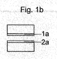
図1bは、接合すべき表面の非晶質化後の、基板1,2の、正しい縮尺ではない概略的な原理図を示している。第1の基板1には、本発明による装置(図示せず)内で、第1の薄い非晶質化層1aを設け、第2の基板2には、本発明による装置(図示せず)内で、第2の薄い非晶質化層2aを設ける。図1bは、例としての方法の第2の方法ステップである。選択的には、両非晶質化層1a,2aのうちの一方を省くことが考えられる。
FIG. 1b shows a schematic, not to scale, schematic diagram of the
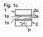
図1cは、接合すべき基板1,2の位置合わせの、正しい縮尺ではない概略的な原理図を示している。第1の非晶質層1aを備えた第1の基板1は、第2の非晶質層2aを備えた第2の基板2に対して相対的に、非晶質層1a,2aが、非晶質層1a,2aの互いに向き合う表面1o,2oに位置するように、互いに位置合わせされている。これにより位置合わせ装置は、明らかに開示されているが、移動方向矢印Pによってシンボルとしてしか図示されていない。図1cは、例としての本発明による方法の第3の方法ステップである。
FIG. 1c shows a schematic diagram of the positioning of the
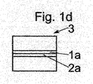
図1dは、接合すべき2つの基板1,2から成る、予備接合により接合された基板積層体3を、正しい縮尺ではない概略的な原理図で示している。非晶質層1a,2aは、予備接合により互いに接合されている。図1dは、第4の方法ステップを示す。
FIG. 1d shows a
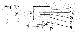
図1eは、基板1,2から形成された基板積層体3の非晶質層1aおよび/または2aへの、本発明による放射5の作用を示している。放射源4が放射5を発生させる。矢印は、放射源4と基板積層体3との間の相対運動をシンボル化して示している。特に放射5は、基板積層体3を格子状に走査する。別の実施形態では、閉ループ制御および/または開ループ制御の相対的な移動の移動軌跡が、特に制御コンピュータ(図示せず)内に格納され、規定の処方として変換することができる。このようにして、熱に敏感な区域を有する基板領域の熱負荷を最小にするために最適化された軌道曲線を生成することができる。軌跡のモデル化および/または計算は、FEMのようなシミュレーション、または熱的・機械的結合モデル化に基づき行うことができる。したがって、上述した全てのパラメータは、放射の入射時間、および入射場所、および入射軌道、および入射強度の規定および/または適合のために利用することができる。図1eは、第5の方法ステップを示す。
FIG. 1e shows the effect of the
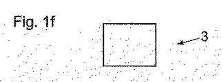
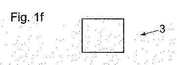
図1fは、本発明による熱処理された基板積層体を概略的な原理図で示しており、この場合図面の縮尺は正確ではない。この場合、本発明により実施された第5の方法ステップで、接合境界面全体もしくは非晶相全体が、結晶相に転移されている。したがって、基板積層体は分離不能に永久的に接合されている。 FIG. 1f shows a heat-treated substrate stack according to the invention in a schematic principle view, in which the drawings are not to scale. In this case, in the fifth method step implemented according to the invention, the entire bonding interface or the entire amorphous phase has been transformed into a crystalline phase. Therefore, the substrate laminate is permanently bonded inseparably.
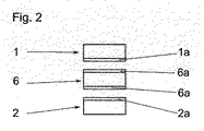
図2は、本発明による方法により別の実施形態で接合される3つの基板1,2,6の概略的な原理図を示しており、この図は正確な縮尺ではない。第1の基板1ならびに第2の基板2はそれぞれ少なくとも1つの非晶質層1a,2aを有している。第3の基板6は、その基板材料が放射に対して透過性である必要はなく、2つの非晶質層6aを有している。基板1ならびに2を基板6に接合した後、両側で同時にまたは時間的にずれて生じる本発明による相転移により、2つよりも多い基板から成る基板積層体(図示せず)が形成され得る。好適には、この場合、3つの基板から成る、有利には4つの基板から成る、特に有利には5つ以上の基板から成る基板積層体が開示された方法により製作される。
FIG. 2 shows a schematic principle diagram of three
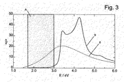
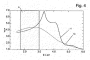
以下のグラフの説明は、計算されたデータに基づき、非晶質シリコンおよび結晶シリコンの吸収率および屈折率の挙動を示す。両グラフは、所定の波長範囲で、シリコンと同じ挙動を示す全ての別の材料のための例示的な例と見なされる。 The description of the graph below shows the behavior of the absorptivity and the refractive index of amorphous silicon and crystalline silicon based on the calculated data. Both graphs are considered as illustrative examples for all other materials that exhibit the same behavior as silicon in a given wavelength range.
図3には、非晶質Si(点線8)および結晶Si(実線9)についての、2つの計算された吸収スペクトルが示されている。グラフは、eVである粒子エネルギ、特に光子エネルギの関数としての吸収率εを示している。実線9は、粒子エネルギに依存した結晶相におけるSiの吸収挙動を示す。点線8は、粒子エネルギに依存した非晶相におけるSiの吸収挙動を示す。約1.8eV〜3.0eVの粒子エネルギ範囲Aでは、非晶相は結晶相よりも0.2〜18倍高い吸収能力を有していることがわかる。1.8eV〜3.0eVの粒子エネルギを有する粒子は、結晶相によっては殆ど吸収されず、非晶相によって極めて強力に吸収される。 FIG. 3 shows two calculated absorption spectra for amorphous Si (dotted line 8) and crystalline Si (solid line 9). The graph shows the absorption ε as a function of the particle energy which is eV, in particular the photon energy. The solid line 9 shows the absorption behavior of Si in the crystal phase depending on the particle energy. The dotted line 8 shows the absorption behavior of Si in the amorphous phase depending on the particle energy. It can be seen that in the particle energy range A of about 1.8 eV to 3.0 eV, the amorphous phase has an absorption capacity 0.2 to 18 times higher than the crystalline phase. Particles having a particle energy of 1.8 eV to 3.0 eV are hardly absorbed by the crystalline phase and are extremely strongly absorbed by the amorphous phase.
すなわち開示された方法は、非晶相の吸収が、結晶相の吸収よりも大きい、特に少なくとも1.1倍大きい、好適には2倍大きい、さらに好適には5倍大きい、さらに好適には10倍大きい、最も好適には20倍大きいスペクトルの範囲を利用する。 That is, the disclosed method provides that the absorption of the amorphous phase is greater than the absorption of the crystalline phase, in particular at least 1.1 times greater, preferably 2 times greater, more preferably 5 times greater, more preferably 10 times greater. A spectral range that is twice as large, most preferably 20 times larger, is utilized.
図4には、非晶質Si(点線10)および結晶Si(実線11)についての、2つの計算された屈折率グラフ10,11が示されている。このグラフは、eVである粒子エネルギ、特に光子エネルギの関数としての屈折率nを示している。約1.8eV〜3.0eVの粒子エネルギ範囲Aでは、非晶質Siと結晶Siの屈折率nが極めて近似していることがわかる。すなわち、もっぱら屈折率に基づく全ての物理的プロセスは、この粒子エネルギ範囲Aでは、非晶質シリコンおよび結晶シリコンにおいて極めて類似している。
FIG. 4 shows two calculated
同様の考察は、非晶相が残留物なしに結晶相に転移され得るならば、非晶質化された相を含む結晶材料混合物にも当てはまる。 Similar considerations apply to a mixture of crystalline materials comprising an amorphized phase, provided that the amorphous phase can be transformed into a crystalline phase without residue.
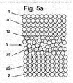
図5aには、相応の非晶質層1a,2aを有した2つの基板1,2の基板積層体3が、正確な縮尺ではなく拡大されて示されている。個々の原子a1,a2が示されており、これらの原子から、基板1,2の結晶相もしくは非晶質層1a,2aの非晶相が構成されている。基板1,2の結晶相の原子a1は規則的であり、非晶相の原子a2は規則的ではない。
FIG. 5a shows the
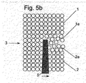
図5bには、放射5により処理される相応の非晶質層1a,2aを有した基板1,2の基板積層体3が、正確な縮尺ではなく拡大されて示されている。放射5は、結晶基板2をほぼ妨げられることなく貫通するが、非晶質層1a,2aによっては吸収される。放射5が既に当てられた領域では既に結晶化されている。
FIG. 5b shows the
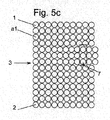
図5cには、相応の非晶質層1a,2aを有さない、ほぼ完全に互いに接合された2つの基板1,2の基板積層体3が、正確な縮尺ではなく拡大されて示されている。図面の右縁部には転位7が見られる。図示した転位7は、刃状転位である。この転位は、その下端部で、当業者には既知のシンボルによりマークされており、かつ付加的に破線で取り囲まれている。刃状転位7は、その他は完璧な格子間に入り込む付加的な原子の列である。転位7の近傍に生じる格子原子の歪みが示されている。このような欠陥は当業者には公知である。このような欠陥が本発明による方法において生じる可能性があるが、必ずしも生じるわけではないことが明言される。
FIG. 5c shows the
1 第1の基板
1a 第1の基板の第1の非晶質層
1o 第1の層の接合表面
2 第2の基板
2a 第2の基板の第2の非晶質層
2o 第2の層の接合表面
3 基板積層体
4 放射の放射源
5 放射
6 第3の基板
6a 第3の基板の非晶質層
7 転位
8,9 吸収スペクトル
10,11 屈折率グラフ
a1,a2 原子
A 粒子エネルギ範囲
ε 吸収率
n 屈折率
P 移動矢印
DESCRIPTION OF
Claims (16)
第1の非晶質層(1a,6a)を前記第1の基板(1,6)上に形成する、かつ/または第2の非晶質層(2a)を前記第2の基板(2)上に形成するステップと、
前記第1の基板(1,6)を前記第2の基板(2)に、1つのまたは複数の前記非晶質層(1a,2a,6a)で接続し、基板積層体(3)を形成するステップと、
前記1つのまたは複数の非晶質層(1a,2a,6a)が1つのまたは複数の結晶層に転移するように、前記1つのまたは複数の非晶質層(1a,2a,6a)を、放射(5)により照射するステップと、
を有する、第1の基板(1,6)を第2の基板(2)に接合する方法。 A method of joining a first substrate (1, 6) to a second substrate (2),
Forming a first amorphous layer (1a, 6a) on the first substrate (1, 6) and / or forming a second amorphous layer (2a) on the second substrate (2); Forming on top;
The first substrate (1, 6) is connected to the second substrate (2) by one or a plurality of the amorphous layers (1a, 2a, 6a) to form a substrate laminate (3). Steps to
The one or more amorphous layers (1a, 2a, 6a) such that the one or more amorphous layers (1a, 2a, 6a) are transformed into one or more crystal layers; Irradiating with radiation (5);
Bonding the first substrate (1, 6) to the second substrate (2).
前記基板(1,2,6)を保持するための保持装置と、
前記基板(1,2,6)を接合するための接合装置と、
照射装置(4)と、
を有しており、
第1の非晶質層(1a,6a)を前記第1の基板(1,6)上に形成可能であり、かつ/または第2の非晶質層(2a)を前記第2の基板(2)上に形成可能であり、
前記第1の基板(1,6)を前記第2の基板(2)に、1つのまたは複数の前記非晶質層(1a,2a,6a)で接続して、基板積層体(3)を形成可能であり、
前記1つのまたは複数の非晶質層(1a,2a,6a)が、1つのまたは複数の結晶層に転移可能であるように、前記照射装置(4)により前記1つのまたは複数の非晶質層(1a,2a,6a)に放射(5)を照射可能である
ように、形成されている、第1の基板(1,6)を第2の基板(2)に接合する装置。 15. An apparatus for joining a first substrate (1, 6) to a second substrate (2), in particular by the method according to any one of claims 1 to 14,
A holding device for holding the substrate (1, 2, 6);
A joining device for joining the substrates (1, 2, 6);
An irradiation device (4);
Has,
A first amorphous layer (1a, 6a) can be formed on the first substrate (1, 6) and / or a second amorphous layer (2a) can be formed on the second substrate (1 2) can be formed on,
The first substrate (1, 6) is connected to the second substrate (2) by one or a plurality of the amorphous layers (1a, 2a, 6a) to form a substrate laminate (3). Formable,
The one or more amorphous layers (1a, 2a, 6a) can be transferred to one or more crystalline layers by the irradiation device (4) such that the one or more amorphous layers (1a, 2a, 6a) can be transferred to one or more crystalline layers. Apparatus for joining a first substrate (1, 6) to a second substrate (2), which is formed so that the layers (1a, 2a, 6a) can be irradiated with radiation (5).
Applications Claiming Priority (1)
| Application Number | Priority Date | Filing Date | Title |
|---|---|---|---|
| PCT/EP2017/053918 WO2018153434A1 (en) | 2017-02-21 | 2017-02-21 | Method and device for bonding substrates |
Publications (1)
| Publication Number | Publication Date |
|---|---|
| JP2020508564A true JP2020508564A (en) | 2020-03-19 |
Family
ID=58108607
Family Applications (1)
| Application Number | Title | Priority Date | Filing Date |
|---|---|---|---|
| JP2019542366A Pending JP2020508564A (en) | 2017-02-21 | 2017-02-21 | Method and apparatus for bonding substrates |
Country Status (7)
| Country | Link |
|---|---|
| US (2) | US10971365B2 (en) |
| EP (1) | EP3586356B1 (en) |
| JP (1) | JP2020508564A (en) |
| KR (1) | KR102615398B1 (en) |
| CN (1) | CN110235223A (en) |
| SG (1) | SG11201906390SA (en) |
| WO (1) | WO2018153434A1 (en) |
Cited By (3)
| Publication number | Priority date | Publication date | Assignee | Title |
|---|---|---|---|---|
| JP2024021511A (en) * | 2022-08-03 | 2024-02-16 | 株式会社Sumco | Bonded silicon wafer and its manufacturing method |
| WO2025109949A1 (en) * | 2023-11-22 | 2025-05-30 | 株式会社サイコックス | Bonded semiconductor substrate and method for manufacturing bonded semiconductor substrate |
| WO2025109948A1 (en) * | 2023-11-22 | 2025-05-30 | 株式会社サイコックス | Bonded semiconductor substrate and method for manufacturing bonded semiconductor substrate |
Families Citing this family (2)
| Publication number | Priority date | Publication date | Assignee | Title |
|---|---|---|---|---|
| US12457751B2 (en) | 2021-07-19 | 2025-10-28 | Taiwan Semiconductor Manufacturing Company, Ltd. | Interfacial layer with high texture uniformity for ferroelectric layer enhancement |
| FR3165103A1 (en) * | 2024-07-25 | 2026-01-30 | Commissariat A L' Energie Atomique Et Aux Energies Alternatives | Covalent bonding process by atomic diffusion to form a conductive bonding interface |
Citations (3)
| Publication number | Priority date | Publication date | Assignee | Title |
|---|---|---|---|---|
| JPH04180674A (en) * | 1990-01-10 | 1992-06-26 | Ricoh Co Ltd | Method for manufacturing semiconductor film |
| JP2015220320A (en) * | 2014-05-16 | 2015-12-07 | 株式会社豊田自動織機 | Semiconductor substrate manufacturing method |
| US20170025306A1 (en) * | 2015-07-21 | 2017-01-26 | Sunedison Semiconductor Limited (Uen201334164H) | Methods for preparing layered semiconductor structures and related bonded structures |
Family Cites Families (37)
| Publication number | Priority date | Publication date | Assignee | Title |
|---|---|---|---|---|
| US5441776A (en) | 1993-11-08 | 1995-08-15 | Sterling; Rodney D. | Silicon dioxide bonding layers and method |
| US20010045352A1 (en) * | 1998-05-14 | 2001-11-29 | Robinson Raymond S. | Sputter deposition using multiple targets |
| US6534381B2 (en) * | 1999-01-08 | 2003-03-18 | Silicon Genesis Corporation | Method for fabricating multi-layered substrates |
| US6881644B2 (en) * | 1999-04-21 | 2005-04-19 | Silicon Genesis Corporation | Smoothing method for cleaved films made using a release layer |
| JP4450126B2 (en) * | 2000-01-21 | 2010-04-14 | 日新電機株式会社 | Method for forming silicon crystal thin film |
| FR2817395B1 (en) * | 2000-11-27 | 2003-10-31 | Soitec Silicon On Insulator | METHOD FOR MANUFACTURING A SUBSTRATE, IN PARTICULAR FOR OPTICS, ELECTRONICS OR OPTOELECTRONICS AND SUBSTRATE OBTAINED THEREBY |
| US6497763B2 (en) * | 2001-01-19 | 2002-12-24 | The United States Of America As Represented By The Secretary Of The Navy | Electronic device with composite substrate |
| WO2003097552A1 (en) * | 2002-04-30 | 2003-11-27 | Agency For Science Technology And Research | A method of wafer/substrate bonding |
| JP3774782B2 (en) * | 2003-05-14 | 2006-05-17 | 富士通メディアデバイス株式会社 | Manufacturing method of surface acoustic wave device |
| US7165712B2 (en) * | 2003-10-23 | 2007-01-23 | Siemens Power Generation, Inc. | Transient liquid phase bonding to cold-worked surfaces |
| JP2005288673A (en) * | 2004-04-06 | 2005-10-20 | Mitsubishi Heavy Ind Ltd | Device for manufacturing micro-structure |
| US7410882B2 (en) | 2004-09-28 | 2008-08-12 | Palo Alto Research Center Incorporated | Method of manufacturing and structure of polycrystalline semiconductor thin-film heterostructures on dissimilar substrates |
| US7565996B2 (en) * | 2004-10-04 | 2009-07-28 | United Technologies Corp. | Transient liquid phase bonding using sandwich interlayers |
| JP2006187685A (en) * | 2004-12-28 | 2006-07-20 | Fuji Xerox Co Ltd | Microstructure, microreactor, heat exchanger and manufacturing method of microstructure |
| US8138061B2 (en) * | 2005-01-07 | 2012-03-20 | International Business Machines Corporation | Quasi-hydrophobic Si-Si wafer bonding using hydrophilic Si surfaces and dissolution of interfacial bonding oxide |
| JP4934966B2 (en) * | 2005-02-04 | 2012-05-23 | 株式会社Sumco | Manufacturing method of SOI substrate |
| US7462552B2 (en) | 2005-05-23 | 2008-12-09 | Ziptronix, Inc. | Method of detachable direct bonding at low temperatures |
| US20080035707A1 (en) * | 2006-08-14 | 2008-02-14 | The Regents Of The University Of California | Transient-liquid-phase joining of ceramics at low temperatures |
| JP4172806B2 (en) * | 2006-09-06 | 2008-10-29 | 三菱重工業株式会社 | Room temperature bonding method and room temperature bonding apparatus |
| US8993410B2 (en) * | 2006-09-08 | 2015-03-31 | Silicon Genesis Corporation | Substrate cleaving under controlled stress conditions |
| FR2921749B1 (en) * | 2007-09-27 | 2014-08-29 | Soitec Silicon On Insulator | METHOD FOR MANUFACTURING A STRUCTURE COMPRISING A SUBSTRATE AND A LAYER DEPOSITED ON ONE OF ITS FACES |
| KR101499175B1 (en) * | 2007-10-04 | 2015-03-05 | 가부시키가이샤 한도오따이 에네루기 켄큐쇼 | Method for manufacturing semiconductor substrate |
| FR2938120B1 (en) * | 2008-10-31 | 2011-04-08 | Commissariat Energie Atomique | PROCESS FOR FORMATION OF A MONOCRYSTALLINE LAYER IN THE MICROELECTRONIC DOMAIN |
| SG162675A1 (en) * | 2008-12-15 | 2010-07-29 | Semiconductor Energy Lab | Manufacturing method of soi substrate and manufacturing method of semiconductor device |
| US8247317B2 (en) * | 2009-09-16 | 2012-08-21 | Applied Materials, Inc. | Methods of solid phase recrystallization of thin film using pulse train annealing method |
| SG194845A1 (en) | 2011-08-30 | 2013-12-30 | Ev Group E Thallner Gmbh | Method for permanent bonding of wafers |
| US9492990B2 (en) * | 2011-11-08 | 2016-11-15 | Picosys Incorporated | Room temperature glass-to-glass, glass-to-plastic and glass-to-ceramic/semiconductor bonding |
| FR2983342B1 (en) * | 2011-11-30 | 2016-05-20 | Soitec Silicon On Insulator | METHOD FOR MANUFACTURING A HETEROSTRUCTURE LIMITING THE DEFECT FORMATION AND HETEROSTRUCTURE THUS OBTAINED |
| WO2013129572A1 (en) * | 2012-02-29 | 2013-09-06 | 京セラ株式会社 | Composite substrate |
| FR2995445B1 (en) * | 2012-09-07 | 2016-01-08 | Soitec Silicon On Insulator | METHOD OF MANUFACTURING A STRUCTURE FOR SUBSEQUENT SEPARATION |
| US9315417B2 (en) | 2013-02-17 | 2016-04-19 | Invenias Inc | Attachment of a cap to a substrate-based device with in situ monitoring of bond quality |
| CN105340070B (en) | 2013-07-05 | 2019-08-16 | Ev 集团 E·索尔纳有限责任公司 | Method for joining metal contact surfaces |
| JP6061251B2 (en) * | 2013-07-05 | 2017-01-18 | 株式会社豊田自動織機 | Manufacturing method of semiconductor substrate |
| CN111261498B (en) | 2014-04-01 | 2024-08-20 | Ev集团E·索尔纳有限责任公司 | Method and device for substrate surface treatment |
| WO2015191112A1 (en) | 2014-06-09 | 2015-12-17 | Dirtt Environmental Solutions Inc. | Associating computer-executable objects with timber frames within an architectural design environment |
| KR102306977B1 (en) | 2014-06-24 | 2021-09-30 | 에베 그룹 에. 탈너 게엠베하 | Method and device for surface treatment of substrates |
| US20180104765A1 (en) * | 2016-10-13 | 2018-04-19 | United Technologies Corporation | Hybrid component and method of making |
-
2017
- 2017-02-21 WO PCT/EP2017/053918 patent/WO2018153434A1/en not_active Ceased
- 2017-02-21 CN CN201780085913.XA patent/CN110235223A/en active Pending
- 2017-02-21 KR KR1020197022649A patent/KR102615398B1/en active Active
- 2017-02-21 SG SG11201906390SA patent/SG11201906390SA/en unknown
- 2017-02-21 US US16/481,994 patent/US10971365B2/en active Active
- 2017-02-21 JP JP2019542366A patent/JP2020508564A/en active Pending
- 2017-02-21 EP EP17706731.1A patent/EP3586356B1/en active Active
-
2021
- 2021-02-12 US US17/174,692 patent/US11862466B2/en active Active
Patent Citations (3)
| Publication number | Priority date | Publication date | Assignee | Title |
|---|---|---|---|---|
| JPH04180674A (en) * | 1990-01-10 | 1992-06-26 | Ricoh Co Ltd | Method for manufacturing semiconductor film |
| JP2015220320A (en) * | 2014-05-16 | 2015-12-07 | 株式会社豊田自動織機 | Semiconductor substrate manufacturing method |
| US20170025306A1 (en) * | 2015-07-21 | 2017-01-26 | Sunedison Semiconductor Limited (Uen201334164H) | Methods for preparing layered semiconductor structures and related bonded structures |
Cited By (4)
| Publication number | Priority date | Publication date | Assignee | Title |
|---|---|---|---|---|
| JP2024021511A (en) * | 2022-08-03 | 2024-02-16 | 株式会社Sumco | Bonded silicon wafer and its manufacturing method |
| JP7782388B2 (en) | 2022-08-03 | 2025-12-09 | 株式会社Sumco | Bonded silicon wafer and manufacturing method thereof |
| WO2025109949A1 (en) * | 2023-11-22 | 2025-05-30 | 株式会社サイコックス | Bonded semiconductor substrate and method for manufacturing bonded semiconductor substrate |
| WO2025109948A1 (en) * | 2023-11-22 | 2025-05-30 | 株式会社サイコックス | Bonded semiconductor substrate and method for manufacturing bonded semiconductor substrate |
Also Published As
| Publication number | Publication date |
|---|---|
| EP3586356B1 (en) | 2023-11-08 |
| SG11201906390SA (en) | 2019-08-27 |
| US10971365B2 (en) | 2021-04-06 |
| KR20190117507A (en) | 2019-10-16 |
| US11862466B2 (en) | 2024-01-02 |
| KR102615398B1 (en) | 2023-12-18 |
| CN110235223A (en) | 2019-09-13 |
| WO2018153434A1 (en) | 2018-08-30 |
| US20210202251A1 (en) | 2021-07-01 |
| US20190393037A1 (en) | 2019-12-26 |
| EP3586356A1 (en) | 2020-01-01 |
Similar Documents
| Publication | Publication Date | Title |
|---|---|---|
| US11862466B2 (en) | Method and device for bonding substrates | |
| JP6061251B2 (en) | Manufacturing method of semiconductor substrate | |
| US10297479B2 (en) | Wafer debonding using mid-wavelength infrared radiation ablation | |
| US9586291B2 (en) | Adhesives for bonding handler wafers to device wafers and enabling mid-wavelength infrared laser ablation release | |
| US8101490B2 (en) | Method for manufacturing semiconductor device and apparatus for manufacturing same | |
| KR102163211B1 (en) | Method of pulsed laser-based large area graphene synthesis on metallic and crystalline substrates | |
| US9336989B2 (en) | Method of cleaving a thin sapphire layer from a bulk material by implanting a plurality of particles and performing a controlled cleaving process | |
| CN111373508B (en) | Method and assembly for ohmic contacts in thinned silicon carbide devices | |
| JP5918160B2 (en) | Gettering semiconductor wafer and manufacturing method thereof | |
| JP6152827B2 (en) | Manufacturing method of semiconductor substrate | |
| TWI762469B (en) | Apparatus and methods to remove unbonded areas within bonded substrates using localized electromagnetic wave annealing | |
| US20220367190A1 (en) | Non-contact processing device and processing method | |
| TW200818321A (en) | Semiconductor on insulator structure made using radiation annealing | |
| JP7420922B2 (en) | bonded substrate | |
| Rasheed et al. | A Review: Laser Annealing of Active SiC and Its Applications | |
| WO2009131061A1 (en) | Method of manufacturing a si(1-v-w-x)cwalxnv substrate, method of manufacturing an epitaxial wafer, si(1-v-w-x)cwalxnv substrate, and epitaxial wafer | |
| Kupo et al. | Features of diamond crystal processing by pulsed laser radiation in microelectronics technologies | |
| JP5738145B2 (en) | Manufacturing method of SOI wafer | |
| KR20250162533A (en) | Method for manufacturing a semiconductor substrate, semiconductor substrate, and semiconductor device | |
| JP2013106024A (en) | Silicon substrate, manufacturing method therefor, and semiconductor device manufacturing method |
Legal Events
| Date | Code | Title | Description |
|---|---|---|---|
| A621 | Written request for application examination |
Free format text: JAPANESE INTERMEDIATE CODE: A621 Effective date: 20200207 |
|
| A977 | Report on retrieval |
Free format text: JAPANESE INTERMEDIATE CODE: A971007 Effective date: 20210114 |
|
| A131 | Notification of reasons for refusal |
Free format text: JAPANESE INTERMEDIATE CODE: A131 Effective date: 20210301 |
|
| A521 | Request for written amendment filed |
Free format text: JAPANESE INTERMEDIATE CODE: A523 Effective date: 20210527 |
|
| A02 | Decision of refusal |
Free format text: JAPANESE INTERMEDIATE CODE: A02 Effective date: 20210914 |