JP2020191376A - Double-sided polishing device carrier and manufacturing method thereof - Google Patents
Double-sided polishing device carrier and manufacturing method thereof Download PDFInfo
- Publication number
- JP2020191376A JP2020191376A JP2019095777A JP2019095777A JP2020191376A JP 2020191376 A JP2020191376 A JP 2020191376A JP 2019095777 A JP2019095777 A JP 2019095777A JP 2019095777 A JP2019095777 A JP 2019095777A JP 2020191376 A JP2020191376 A JP 2020191376A
- Authority
- JP
- Japan
- Prior art keywords
- insert member
- double
- carrier
- inner peripheral
- holding hole
- Prior art date
- Legal status (The legal status is an assumption and is not a legal conclusion. Google has not performed a legal analysis and makes no representation as to the accuracy of the status listed.)
- Pending
Links
Images


Classifications
-
- B—PERFORMING OPERATIONS; TRANSPORTING
- B24—GRINDING; POLISHING
- B24B—MACHINES, DEVICES, OR PROCESSES FOR GRINDING OR POLISHING; DRESSING OR CONDITIONING OF ABRADING SURFACES; FEEDING OF GRINDING, POLISHING, OR LAPPING AGENTS
- B24B37/00—Lapping machines or devices; Accessories
- B24B37/04—Lapping machines or devices; Accessories designed for working plane surfaces
- B24B37/07—Lapping machines or devices; Accessories designed for working plane surfaces characterised by the movement of the work or lapping tool
- B24B37/08—Lapping machines or devices; Accessories designed for working plane surfaces characterised by the movement of the work or lapping tool for double side lapping
-
- B—PERFORMING OPERATIONS; TRANSPORTING
- B24—GRINDING; POLISHING
- B24B—MACHINES, DEVICES, OR PROCESSES FOR GRINDING OR POLISHING; DRESSING OR CONDITIONING OF ABRADING SURFACES; FEEDING OF GRINDING, POLISHING, OR LAPPING AGENTS
- B24B37/00—Lapping machines or devices; Accessories
- B24B37/27—Work carriers
- B24B37/28—Work carriers for double side lapping of plane surfaces
-
- B—PERFORMING OPERATIONS; TRANSPORTING
- B24—GRINDING; POLISHING
- B24B—MACHINES, DEVICES, OR PROCESSES FOR GRINDING OR POLISHING; DRESSING OR CONDITIONING OF ABRADING SURFACES; FEEDING OF GRINDING, POLISHING, OR LAPPING AGENTS
- B24B47/00—Drives or gearings; Equipment therefor
- B24B47/10—Drives or gearings; Equipment therefor for rotating or reciprocating working-spindles carrying grinding wheels or workpieces
- B24B47/12—Drives or gearings; Equipment therefor for rotating or reciprocating working-spindles carrying grinding wheels or workpieces by mechanical gearing or electric power
-
- B—PERFORMING OPERATIONS; TRANSPORTING
- B24—GRINDING; POLISHING
- B24B—MACHINES, DEVICES, OR PROCESSES FOR GRINDING OR POLISHING; DRESSING OR CONDITIONING OF ABRADING SURFACES; FEEDING OF GRINDING, POLISHING, OR LAPPING AGENTS
- B24B7/00—Machines or devices designed for grinding plane surfaces on work, including polishing plane glass surfaces; Accessories therefor
- B24B7/20—Machines or devices designed for grinding plane surfaces on work, including polishing plane glass surfaces; Accessories therefor characterised by a special design with respect to properties of the material of non-metallic articles to be ground
- B24B7/22—Machines or devices designed for grinding plane surfaces on work, including polishing plane glass surfaces; Accessories therefor characterised by a special design with respect to properties of the material of non-metallic articles to be ground for grinding inorganic material, e.g. stone, ceramics, porcelain
- B24B7/228—Machines or devices designed for grinding plane surfaces on work, including polishing plane glass surfaces; Accessories therefor characterised by a special design with respect to properties of the material of non-metallic articles to be ground for grinding inorganic material, e.g. stone, ceramics, porcelain for grinding thin, brittle parts, e.g. semiconductors, wafers
-
- B—PERFORMING OPERATIONS; TRANSPORTING
- B29—WORKING OF PLASTICS; WORKING OF SUBSTANCES IN A PLASTIC STATE IN GENERAL
- B29C—SHAPING OR JOINING OF PLASTICS; SHAPING OF MATERIAL IN A PLASTIC STATE, NOT OTHERWISE PROVIDED FOR; AFTER-TREATMENT OF THE SHAPED PRODUCTS, e.g. REPAIRING
- B29C45/00—Injection moulding, i.e. forcing the required volume of moulding material through a nozzle into a closed mould; Apparatus therefor
- B29C45/14—Injection moulding, i.e. forcing the required volume of moulding material through a nozzle into a closed mould; Apparatus therefor incorporating preformed parts or layers, e.g. injection moulding around inserts or for coating articles
- B29C45/14467—Joining articles or parts of a single article
-
- H—ELECTRICITY
- H01—ELECTRIC ELEMENTS
- H01L—SEMICONDUCTOR DEVICES NOT COVERED BY CLASS H10
- H01L21/00—Processes or apparatus adapted for the manufacture or treatment of semiconductor or solid state devices or of parts thereof
- H01L21/67—Apparatus specially adapted for handling semiconductor or electric solid state devices during manufacture or treatment thereof; Apparatus specially adapted for handling wafers during manufacture or treatment of semiconductor or electric solid state devices or components ; Apparatus not specifically provided for elsewhere
- H01L21/67005—Apparatus not specifically provided for elsewhere
- H01L21/67011—Apparatus for manufacture or treatment
- H01L21/67092—Apparatus for mechanical treatment
-
- B—PERFORMING OPERATIONS; TRANSPORTING
- B29—WORKING OF PLASTICS; WORKING OF SUBSTANCES IN A PLASTIC STATE IN GENERAL
- B29L—INDEXING SCHEME ASSOCIATED WITH SUBCLASS B29C, RELATING TO PARTICULAR ARTICLES
- B29L2031/00—Other particular articles
- B29L2031/736—Grinding or polishing equipment
Abstract
Description
本発明は、半導体ウェーハ(以下、単にウェーハとも言う)の両面研磨装置用キャリアおよびその製造方法に関する。 The present invention relates to a carrier for a double-sided polishing apparatus for a semiconductor wafer (hereinafter, also simply referred to as a wafer) and a method for manufacturing the same.
両面研磨装置は通常、不織布や発砲ウレタン等からなる研磨布が貼付された上定盤と下定盤を具備し、中心部にはサンギア、外周部にはインターナルギアがそれぞれ配置された遊星歯車構造を有する、いわゆる4ウェイ方式のものが用いられている。ウェーハを研磨する場合には、キャリアに形成されたウェーハ保持孔(以下、単に保持孔とも言う)の内部にウェーハを挿入して保持する。上定盤側から研磨スラリーをウェーハに供給し、上下の定盤を回転させて、上定盤と下定盤の対向する研磨布をウェーハの表裏両面に押し付けながら、キャリアをサンギアとインターナルギアとの間で自公転運動させることで各ウェーハの両面を同時に研磨することができる。 A double-sided polishing device usually has an upper surface plate and a lower surface plate to which a polishing cloth made of non-woven fabric or urethane foam is attached, and has a planetary gear structure in which a sun gear is arranged in the center and an internal gear is arranged in the outer periphery. A so-called 4-way system having a so-called 4-way system is used. When polishing a wafer, the wafer is inserted and held inside a wafer holding hole (hereinafter, also simply referred to as a holding hole) formed in the carrier. The polishing slurry is supplied to the wafer from the upper surface plate side, the upper and lower surface plates are rotated, and the polishing cloths facing the upper surface plate and the lower surface plate are pressed against both the front and back surfaces of the wafer, while the carrier is held between the sun gear and the internal gear. Both sides of each wafer can be polished at the same time by rotating and revolving between them.
ウェーハを保持するための保持孔を有する両面研磨装置用キャリア本体はSK鋼やステンレス、チタンなどの金属製のキャリアが主流である。ウェーハの外周部と金属製のキャリアを直接接触させると、ウェーハに割れやキズが生じてしまう可能性がある。そこで、ウェーハ外周部の保護のために、キャリアのウェーハ保持孔の内周部にはインサート部材と呼ばれる樹脂製のリングを有している。このインサート部材の樹脂は嵌め込みによる接着加工又は射出成形により形成されている。インサート部材はウェーハの外周部と接するため、ウェーハのエッジ形状を作り込む上で重要となる。 The mainstream carrier body for a double-sided polishing machine having holding holes for holding a wafer is a carrier made of metal such as SK steel, stainless steel, or titanium. Direct contact between the outer periphery of the wafer and the metal carrier may cause cracks or scratches on the wafer. Therefore, in order to protect the outer peripheral portion of the wafer, a resin ring called an insert member is provided on the inner peripheral portion of the wafer holding hole of the carrier. The resin of this insert member is formed by adhesive processing by fitting or injection molding. Since the insert member is in contact with the outer peripheral portion of the wafer, it is important for forming the edge shape of the wafer.
このインサート部材に関しては、インサート部材形成時やウェーハ加工時、またキャリア搬送時に、インサート部材がずれたり脱落したりすることを防止するために、インサート部材の外周部とキャリアの保持孔の内周部は楔状に嵌合しているものがある。先行技術ではキャリア端面(保持孔の内周面)に溝加工や突出加工、傾斜加工を施すことで上下方向のずれや脱落を防ぐような文献がある(特許文献1−5参照)。 Regarding this insert member, in order to prevent the insert member from slipping or falling off during formation of the insert member, processing of the wafer, and transfer of the carrier, the outer peripheral portion of the insert member and the inner peripheral portion of the holding hole of the carrier Some are fitted in a wedge shape. In the prior art, there is a document in which the end face of the carrier (inner peripheral surface of the holding hole) is grooved, projected, or tilted to prevent vertical displacement or dropout (see Patent Document 1-5).
インサートのずれや脱落の防止のためにインサート部材とキャリア本体の接合部が楔状に嵌合したものは、上下に対するインサート部材のずれや脱落に関しては効果が少なく、上下方向の接着強度の向上が求められている。また、キャリア本体の主面に対してキャリア本体の保持孔の内周面の角度が傾いているようなテーパ形状の場合、使用しているうちにテーパ形状に沿ってインサート部材がずれてしまうことや、インサート部材の形成時にもインサート部材がキャリア本体に対して上下にずれた状態で形成されてしまうことがある。 If the joint between the insert member and the carrier body is fitted in a wedge shape to prevent the insert from slipping or falling off, it has little effect on the slipping or falling off of the insert member with respect to the top and bottom, and it is required to improve the adhesive strength in the vertical direction. Has been done. Further, in the case of a tapered shape in which the angle of the inner peripheral surface of the holding hole of the carrier main body is tilted with respect to the main surface of the carrier main body, the insert member may shift along the tapered shape during use. Further, even when the insert member is formed, the insert member may be formed in a state of being vertically displaced from the carrier body.
ここで従来の両面研磨装置用キャリアの問題点について図4の断面図を参照して説明する。この例では、従来のキャリア101は、キャリア本体102の主面106に対して保持孔103の内周面104の角度が多少傾いてテーパ形状となっている。従来品では、図4のように、インサート部材105の形成時にインサート部材105が上下にずれて形成されてしまうことや、使用時に上下にずれた状態で研磨を行ってしまうことがある。
Here, the problems of the conventional carrier for a double-sided polishing machine will be described with reference to the cross-sectional view of FIG. In this example, the
本発明は前述のような問題に鑑みてなされたもので、インサート部材の上下方向に対する結合強度が高く、ずれや脱落を防止することができ、インサート部材の形成時にキャリア本体に対してインサート部材のずれが抑制された両面研磨装置用キャリアおよびその製造方法を提供することを目的とする。 The present invention has been made in view of the above-mentioned problems, and the coupling strength of the insert member in the vertical direction is high, slippage and dropout can be prevented, and the insert member is attached to the carrier body when the insert member is formed. An object of the present invention is to provide a carrier for a double-sided polishing machine in which deviation is suppressed and a method for manufacturing the same.
上記目的を達成するために、本発明は、半導体ウェーハを両面研磨する両面研磨装置において、研磨布がそれぞれ貼付された上下定盤の間に配設され、研磨の際に前記上下定盤の間に挟まれた前記半導体ウェーハを保持する両面研磨装置用キャリアであって、
前記半導体ウェーハを保持するための保持孔が形成された金属製のキャリア本体と、前記保持孔の内周面に接して配置される樹脂製のインサート部材を有し、
前記インサート部材と接する前記保持孔の内周面の表面粗さRaが1.0μm以上であることを特徴とする両面研磨装置用キャリアを提供する。
In order to achieve the above object, the present invention is a double-sided polishing apparatus for double-sided polishing of a semiconductor wafer, in which polishing cloths are arranged between upper and lower surface plates to which polishing cloths are attached, and between the upper and lower surface plates during polishing. A carrier for a double-sided polishing machine that holds the semiconductor wafer sandwiched between the wafers.
It has a metal carrier body in which a holding hole for holding the semiconductor wafer is formed, and a resin insert member arranged in contact with the inner peripheral surface of the holding hole.
Provided is a carrier for a double-sided polishing machine characterized in that the surface roughness Ra of the inner peripheral surface of the holding hole in contact with the insert member is 1.0 μm or more.
このようにキャリア本体の保持孔の内周面の表面粗さが粗く、表面粗さRa(JIS規格の算術平均粗さ)が1.0μm以上であることにより、キャリア本体とインサート部材の結合強度を向上させることができ、インサート部材の形成時やウェーハ研磨時等において、インサート部材の上下方向のずれを抑制することができる。 As described above, the surface roughness of the inner peripheral surface of the holding hole of the carrier body is rough, and the surface roughness Ra (arithmetic mean roughness of JIS standard) is 1.0 μm or more, so that the bonding strength between the carrier body and the insert member is strong. It is possible to suppress the vertical displacement of the insert member during the formation of the insert member, the polishing of the wafer, and the like.
また、前記インサート部材と接する前記保持孔の内周面の表面粗さRzが5.0μm以上であるものとすることができる。 Further, the surface roughness Rz of the inner peripheral surface of the holding hole in contact with the insert member can be 5.0 μm or more.
このように、さらに表面粗さRz(JIS規格の最大高さ粗さ)が5.0μm以上であれば、より一層、インサート部材の上下方向のずれを抑制することができる。 As described above, when the surface roughness Rz (maximum height roughness of JIS standard) is 5.0 μm or more, the displacement of the insert member in the vertical direction can be further suppressed.
また、前記インサート部材と接する前記保持孔の内周面は、前記キャリア本体の主面に対して垂直であるものとすることができる。 Further, the inner peripheral surface of the holding hole in contact with the insert member may be perpendicular to the main surface of the carrier body.
このようにキャリア本体の主面に対して保持孔の内周面の角度が垂直であれば、テーパ形状の場合に比べて、キャリア本体の上下どちらかにインサート部材の位置が偏ることやずれていくことをより一層防止できる。 If the angle of the inner peripheral surface of the holding hole is perpendicular to the main surface of the carrier body in this way, the position of the insert member is biased or displaced to either the top or bottom of the carrier body as compared with the case of the tapered shape. It can be further prevented from going.
また、前記インサート部材は、
射出成形によるインサート材からなるもの、
または、インサート材と、該インサート材と前記保持孔の内周面との間の接着層からなるものであることができる。
Further, the insert member is
Made of injection molded insert material,
Alternatively, it may consist of an insert material and an adhesive layer between the insert material and the inner peripheral surface of the holding hole.
このように本発明の両面研磨装置は、インサート部材がインサート材の射出成形によるもの、インサート材と接着層からなるもののどちらにも適応でき、インサート部材のずれを抑制可能である。 As described above, the double-sided polishing apparatus of the present invention can be applied to both the insert member formed by injection molding of the insert material and the insert member composed of the insert material and the adhesive layer, and can suppress the displacement of the insert member.
また本発明は、半導体ウェーハを両面研磨する両面研磨装置において、研磨布がそれぞれ貼付された上下定盤の間に配設され、研磨の際に前記上下定盤の間に挟まれた前記半導体ウェーハを保持する両面研磨装置用キャリアを製造する方法であって、
前記半導体ウェーハを保持するための保持孔を金属製のキャリア本体に形成し、前記保持孔の内周面に接してインサート部材を形成するとき、
前記インサート部材と接することになる前記保持孔の内周面の表面粗さRaを1.0μm以上にした上で、前記インサート部材を形成することを特徴とする両面研磨装置用キャリアの製造方法を提供する。
Further, according to the present invention, in a double-sided polishing apparatus for polishing a semiconductor wafer on both sides, the semiconductor wafer is arranged between upper and lower surface plates to which a polishing cloth is attached, and is sandwiched between the upper and lower surface plates during polishing. It is a method of manufacturing a carrier for a double-sided polishing machine that holds a surface plate.
When a holding hole for holding the semiconductor wafer is formed in a metal carrier body and the insert member is formed in contact with the inner peripheral surface of the holding hole.
A method for manufacturing a carrier for a double-sided polishing machine, which comprises forming the insert member after setting the surface roughness Ra of the inner peripheral surface of the holding hole to be in contact with the insert member to 1.0 μm or more. provide.
このようにすれば、キャリア本体とインサート部材の結合強度が向上し、インサート部材の形成時やウェーハ研磨時等において、インサート部材の上下方向のずれを抑制可能な両面研磨装置用キャリアを得ることができる。 By doing so, the bonding strength between the carrier body and the insert member is improved, and it is possible to obtain a carrier for a double-sided polishing device capable of suppressing vertical displacement of the insert member during formation of the insert member, wafer polishing, and the like. it can.
このとき、前記インサート部材と接することになる前記保持孔の内周面の表面粗さRzを5.0μm以上にした上で、前記インサート部材を形成することができる。 At this time, the insert member can be formed after the surface roughness Rz of the inner peripheral surface of the holding hole that comes into contact with the insert member is set to 5.0 μm or more.
このようにすれば、より一層、インサート部材の上下方向のずれを抑制することができる。 By doing so, it is possible to further suppress the vertical displacement of the insert member.
また、前記インサート部材と接することになる前記保持孔の内周面を、前記キャリア本体の主面に対して垂直にした上で、前記インサート部材を形成することができる。 Further, the insert member can be formed after the inner peripheral surface of the holding hole that comes into contact with the insert member is made perpendicular to the main surface of the carrier body.
このようにすれば、テーパ形状の場合に比べて、キャリア本体の上下どちらかへのインサート部材のずれをより一層防止できる。 By doing so, it is possible to further prevent the insert member from shifting to either the upper or lower side of the carrier body as compared with the case of the tapered shape.
また、前記インサート部材を、インサート材の射出成形により形成するか、または、接着剤を使用したインサート材の接着加工により形成することができる。 Further, the insert member can be formed by injection molding of the insert material or by adhesive processing of the insert material using an adhesive.
このように本発明の両面研磨装置用キャリアの製造方法は、インサート部材の形成に関し、インサート材の射出成形や接着加工のどちらにも適応でき、インサート部材のずれを抑制可能である。 As described above, the method for manufacturing a carrier for a double-sided polishing machine of the present invention can be applied to both injection molding and adhesive processing of an insert material for forming an insert member, and can suppress displacement of the insert member.
本発明の両面研磨装置用キャリアおよびその製造方法であれば、キャリア本体とインサート部材の結合強度の向上を図ることができ、インサート部材の形成時やウェーハ研磨時等において、インサート部材の上下方向のずれが生じるのを抑制可能である。 With the carrier for a double-sided polishing apparatus of the present invention and the method for manufacturing the same, it is possible to improve the bonding strength between the carrier body and the insert member, and the insert member is formed in the vertical direction during formation of the insert member, wafer polishing, and the like. It is possible to suppress the occurrence of deviation.
以下、本発明について図面を参照して実施の形態を説明するが、本発明はこれに限定されるものではない。
図1は本発明の両面研磨装置用キャリア(以下、単にキャリアとも言う)の上面図である。また、図2に該キャリアの断面図を示す。
本発明のキャリア1は、図1に示すようにウェーハを保持する保持孔3が形成された金属製のキャリア本体2と、この保持孔3の内周面4に接して配置されている樹脂製のインサート部材5を有している。
Hereinafter, embodiments of the present invention will be described with reference to the drawings, but the present invention is not limited thereto.
FIG. 1 is a top view of the carrier for a double-sided polishing machine of the present invention (hereinafter, also simply referred to as a carrier). Further, FIG. 2 shows a cross-sectional view of the carrier.
As shown in FIG. 1, the
ここで、キャリア本体2の材質としては例えばSK鋼やステンレス、チタンなどが挙げられる。
また、インサート部材5の樹脂(インサート材7)にはエポキシ系やビニル系、ポリスチレン系、アクリル系、ポリアミド(ナイロン)系、ポリイミド系、ポリアセタール、ポリカーボネイト、ポリエチレンテレフタレート、シクロオレフィン系、フッ素系(テフロン(登録商標))などから構成される樹脂を使用することができる。
Here, examples of the material of the
The resin (insert material 7) of the
そして、本発明のキャリア1においては、保持孔3の内周面4の表面粗さRaが1.0μm以上である。このような内周面4であれば、キャリア本体2とインサート部材5の結合強度が従来品に比べて高いものとなる。これらの結合強度が高いため、インサート部材の形成時を含め、ウェーハ研磨時、キャリア搬送時など種々の場合において、保持孔3の内周面4に対するインサート部材5の上下方向(キャリア本体2の主面6に垂直な方向)のずれを抑制することができる。インサート部材5はウェーハ研磨時にウェーハと接するため、ウェーハのエッジ形状の形成において、上記ずれを抑制することは重要である。したがってこのずれを効果的に抑制可能な本発明のキャリア1は極めて有意義である。
なお、内周面4のRaの上限値は特に限定されない。粗いほどインサート部材5との結合強度を高いものとすることができるが、5μmもあれば十分である。
In the
The upper limit of Ra of the inner
また、Raが上記条件を満たす他、内周面4の表面粗さRzが5.0μm以上であるのが好ましい。このようなものであれば、より一層、インサート部材5の上下方向のずれを抑制可能である。
なお、内周面4のRzの上限値は特に限定されない。粗いほどインサート部材5との結合強度を高いものとすることができるが、20μmもあれば十分である。
Further, it is preferable that Ra satisfies the above condition and the surface roughness Rz of the inner
The upper limit of Rz of the inner
また、キャリア本体2の主面6に対する内周面4の角度は垂直であるのが好ましい。上記のように少なくとも内周面4の表面粗さRaが1.0μm以上であれば、内周面4がたとえテーパ形状であってもインサート部材5のずれを従来に比べて十分に抑制可能である。しかし、キャリア本体2の主面6に対して垂直であると、テーパ形状の場合に比べ、ずれをより効果的に抑制することができる。
Further, it is preferable that the angle of the inner
なお、インサート部材5は、たとえば射出成形によるインサート材7からなるものとすることができる。前述したような種類の樹脂をキャリア本体2の保持孔3の内周面4に対して直接射出して成形したものとすることができる。なお、図1ではこの射出成形による例を示している。
The
また、インサート部材5に関して別の例を図3に示す。図3は本発明の両面研磨装置用キャリアの別の例の上面図である。この例のキャリア1Aに示すように、インサート部材5は、インサート材7および接着層8からなっている。接着層8は、内周面4とインサート材7との間に位置しており、この2つを結合している。接着剤の種類は特に限定されないが、たとえば、エポキシ系接着剤などが挙げられる。
保持孔3の内周面4とインサート材7が射出成形により結合されたもの、接着層8を介して結合されたもののいずれにも本発明は対応可能であり、インサート部材5(インサート材7)の上下方向のずれを抑制可能である。
Further, another example of the
The present invention can be applied to both the inner
次に、上記本発明の両面研磨装置用キャリア1を備えた両面研磨装置について説明する。
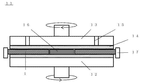
図5は本発明の両面研磨装置用キャリアを備えた両面研磨装置の一例の縦断面図であり、図6は平面視による両面研磨装置の内部構造図である。
図5、6に示すように、1つ以上のキャリア1(ここでは3つ)を具備した両面研磨装置11は、上下に相対向して設けられた下定盤12と上定盤13を備えており、各定盤12、13の対向面側には、それぞれ研磨布14が貼付されている。
また、上定盤13の上部には、上定盤13と下定盤12の間にスラリーを供給するスラリーホール15が設けられている。
なお、図5、6に示すように、上定盤13と下定盤12の間の中心部にはサンギア16が、周縁部にはインターナルギア17が設けられており、4way式の両面研磨装置である。
Next, the double-sided polishing apparatus provided with the
FIG. 5 is a vertical cross-sectional view of an example of a double-sided polishing machine provided with a carrier for a double-sided polishing machine of the present invention, and FIG. 6 is an internal structural view of the double-sided polishing machine in a plan view.
As shown in FIGS. 5 and 6, the double-
Further, above the upper surface plate 13, a
As shown in FIGS. 5 and 6, a
そして、サンギア16及びインターナルギア17の各歯部(不図示)にはキャリア1の外周歯(不図示)が噛合しており、上定盤13及び下定盤12が不図示の駆動源によって回転されるのに伴い、キャリア1は自転しつつサンギア16の周りを公転する。
なお、半導体ウェーハWを両面研磨する際には、ウェーハWはキャリア1の保持孔3で保持されており、上下定盤12、13の回転によりウェーハWを保持したキャリア1は自公転し、上下の研磨布14によりウェーハWの両面が同時に研磨される。なお、研磨時には、スラリーホール15からスラリーが供給される。
The outer teeth (not shown) of the
When the semiconductor wafer W is polished on both sides, the wafer W is held by the holding
次に、本発明の両面研磨装置用キャリア1の製造方法について説明する。
まず、キャリア本体2のために用意した金属プレートに保持孔3を加工して形成する。加工方法は特に限定されないが、例えば、レーザー加工、マシニング加工、ルータ加工、フライス加工、ワイヤ放電加工などで加工することができる。
このとき、保持孔3の内周面4の表面粗さRaが1.0μm以上になるように加工する。内周面4の表面粗さを粗くする方法に関しても限定しないが、上記加工条件による調整の他、追加工によって粗くすることもできる。例えば、ワイヤ放電加工で一旦保持孔3を形成した後、追加工としてルータ加工を施して保持孔3の内周面4の表面粗さ調整を行うことができる。さらに好ましくは内周面4の表面粗さRzが5.0μm以上になるように加工する。
また、保持孔3の加工の際、その内周面4がキャリア本体2の主面6に対して斜めに傾斜(テーパ形状)になるように加工しても良いが、垂直になるように加工するとより好ましい。
Next, a method for manufacturing the
First, the holding
At this time, the inner
Further, when processing the
このように少なくとも保持孔3の内周面4の表面粗さRaが上記数値範囲になるように加工した上で、この粗い内周面4に接するインサート部材5を形成する。本発明の製造方法では、粗く形成した内周面4にインサート部材5を形成するので、内周面4とインサート部材5の結合強度を高くすることができる。その結果、インサート部材5の上下方向のずれを抑制可能である。また、Raの調整の他、Rzの調整、キャリア本体2の主面6に対する形成角度の調整を上記のように行うことで、より一層効果的に上記ずれを抑制することができる。
In this way, the
インサート部材5の形成方法自体は特に限定されず、例えば、粗い内周面4に対して直接的にインサート材7を射出成形することができる。あるいは、接着剤を使用し、保持孔3に嵌合するインサート材7を内周面4に接着加工して形成することも可能である。
いずれの方法で形成した場合でも、上記ずれを抑制することができる。
The method of forming the
Regardless of which method is used, the above-mentioned deviation can be suppressed.
以下、本発明の実施例及び比較例を示して本発明をより具体的に説明するが、本発明はこれらに限定されるものではない。
(実施例1−8、比較例1−2)
比較例1、2として、レーザー加工により、保持孔の内周面がテーパ形状であり、表面粗さが小さい水準(Raはいずれも1.0μm未満)のキャリア本体を準備した。
実施例1−6、8には、ワイヤ放電加工で、保持孔の内周面を垂直に加工して、ルータ加工による追加工で表面粗さが大きい水準(Raはいずれも1.0μm以上)のキャリア本体をそれぞれ準備した。また、実施例7では、保持孔の内周面がテーパ形状であること以外は、実施例1と同様にしてキャリア本体を準備した。
これらのキャリア本体の材質はチタンである。
Hereinafter, the present invention will be described in more detail with reference to Examples and Comparative Examples of the present invention, but the present invention is not limited thereto.
(Example 1-8, Comparative Example 1-2)
As Comparative Examples 1 and 2, a carrier body having a tapered inner peripheral surface of the holding hole and a small surface roughness (Ra is less than 1.0 μm) was prepared by laser processing.
In Examples 1-6 and 8, the inner peripheral surface of the holding hole is vertically machined by wire electric discharge machining, and the surface roughness is large by additional machining by router machining (Ra is 1.0 μm or more in each case). We prepared each carrier body. Further, in Example 7, the carrier body was prepared in the same manner as in Example 1 except that the inner peripheral surface of the holding hole had a tapered shape.
The material of these carrier bodies is titanium.
これらのキャリア本体に対して射出成形または接着加工によりインサート部材を形成した。射出成形ではインサート材としてシクロオレフィンコポリマーを使用した。また接着加工ではガラスエポキシ樹脂製インサート材をエポキシ系接着剤により接着した。 An insert member was formed on these carrier bodies by injection molding or adhesive processing. In injection molding, a cycloolefin copolymer was used as an insert material. In the bonding process, the glass epoxy resin insert material was bonded with an epoxy adhesive.
保持孔の内周面の表面粗さ測定およびインサート部材のずれの確認は、ミツトヨ製の表面粗さ測定器サーフテストにより実施した。
また、インサート部材を形成後のインサート材の接着の強度に関しては、イマダ製のフォースゲージにより剥離強度を測定した。
表1(射出成形の場合)、表2(接着加工の場合)に各水準の表面粗さRa、Rzや、垂直・テーパの分類、剥離強度、インサート材のズレ量を示す。なお、射出成形では比較例1の値で、接着加工では比較例2の値で規格化した剥離強度やインサート材のズレ量も併せて示した。
なお、図7、8に、射出成形の場合の剥離強度、インサート材のズレ量のグラフを示す。また、図9、10に、接着加工の場合の剥離強度、インサート材のズレ量のグラフを示す。
The surface roughness of the inner peripheral surface of the holding hole was measured and the displacement of the insert member was confirmed by the surface roughness measuring instrument surf test manufactured by Mitutoyo.
Regarding the adhesive strength of the insert material after forming the insert member, the peel strength was measured with a force gauge manufactured by Imada.
Table 1 (in the case of injection molding) and Table 2 (in the case of adhesive processing) show the surface roughness Ra and Rz of each level, the classification of vertical / taper, the peel strength, and the amount of deviation of the insert material. In addition, the peel strength standardized by the value of Comparative Example 1 in injection molding and the value of Comparative Example 2 in adhesive processing and the amount of deviation of the insert material are also shown.
Note that FIGS. 7 and 8 show graphs of the peel strength and the amount of displacement of the insert material in the case of injection molding. Further, FIGS. 9 and 10 show graphs of the peel strength and the amount of deviation of the insert material in the case of adhesive processing.
射出成形によるインサート部材形成では、表1、図7、8に示すように従来品の比較例と比べてインサート材の剥離強度が約1.5〜2.3倍向上して、インサート材のズレ量も約50〜80%抑制することができた。
接着加工によるインサート部材形成でも同様に、表2、図9、10に示すように剥離強度が約1.8〜2.2倍向上し、インサート材のズレ量も約50〜70%抑制できた。
また、実施例同士を比較して分かるように、基本的に表面粗さが大きいほど剥離強度が大きくなりズレ量が小さくなるのが分かる。さらには、表面粗さがほぼ同程度の実施例3、7を比べて分かるように、保持孔の内周面がテーパ形状よりも垂直の方が、よりずれにくいことが分かる。
以上から本発明によりキャリア本体に対するインサート材の脱落防止とズレの抑制が可能となった。
In the formation of the insert member by injection molding, as shown in Tables 1, 7 and 8, the peel strength of the insert material is improved by about 1.5 to 2.3 times as compared with the comparative example of the conventional product, and the insert material is displaced. The amount could also be suppressed by about 50-80%.
Similarly, in the formation of the insert member by the adhesive process, the peel strength was improved by about 1.8 to 2.2 times and the amount of displacement of the insert material was suppressed by about 50 to 70% as shown in Tables 2, 9 and 10. ..
Further, as can be seen by comparing the examples, it can be seen that basically, the larger the surface roughness, the larger the peel strength and the smaller the amount of deviation. Furthermore, as can be seen by comparing Examples 3 and 7 having substantially the same surface roughness, it can be seen that the vertical inner peripheral surface of the holding hole is less likely to shift than the tapered shape.
From the above, according to the present invention, it is possible to prevent the insert material from falling off from the carrier body and to suppress the displacement.
なお、本発明は、上記実施形態に限定されるものではない。上記実施形態は、例示であり、本発明の特許請求の範囲に記載された技術的思想と実質的に同一な構成を有し、同様な作用効果を奏するものは、いかなるものであっても本発明の技術的範囲に包含される。 The present invention is not limited to the above embodiment. The above embodiment is an example, and any one having substantially the same configuration as the technical idea described in the claims of the present invention and exhibiting the same effect and effect is the present invention. It is included in the technical scope of the invention.
1、1A…本発明の両面研磨装置用キャリア、 2…キャリア本体、 3…保持孔、
4…保持孔の内周面、 5…インサート部材、 6…キャリア本体の主面、
7…インサート材、 8…接着層、
11…両面研磨装置、 12…下定盤、 13…上定盤、 14…研磨布、
15…スラリーホール、 16…サンギア、 17…インターナルギア、
W…半導体ウェーハ。
1, 1A ... Carrier for double-sided polishing machine of the present invention, 2 ... Carrier body, 3 ... Holding hole,
4 ... Inner peripheral surface of holding hole, 5 ... Insert member, 6 ... Main surface of carrier body,
7 ... Insert material, 8 ... Adhesive layer,
11 ... Double-sided polishing device, 12 ... Lower surface plate, 13 ... Upper surface plate, 14 ... Abrasive cloth,
15 ... Slurry hole, 16 ... Sun gear, 17 ... Internal gear,
W ... Semiconductor wafer.
Claims (8)
前記半導体ウェーハを保持するための保持孔が形成された金属製のキャリア本体と、前記保持孔の内周面に接して配置される樹脂製のインサート部材を有し、
前記インサート部材と接する前記保持孔の内周面の表面粗さRaが1.0μm以上であることを特徴とする両面研磨装置用キャリア。 In a double-sided polishing device for double-sided polishing of a semiconductor wafer, double-sided polishing in which a polishing cloth is arranged between upper and lower surface plates to which a polishing cloth is attached and holds the semiconductor wafer sandwiched between the upper and lower surface plates during polishing. A carrier for equipment
It has a metal carrier body in which a holding hole for holding the semiconductor wafer is formed, and a resin insert member arranged in contact with the inner peripheral surface of the holding hole.
A carrier for a double-sided polishing machine, characterized in that the surface roughness Ra of the inner peripheral surface of the holding hole in contact with the insert member is 1.0 μm or more.
射出成形によるインサート材からなるもの、
または、インサート材と、該インサート材と前記保持孔の内周面との間の接着層からなるものであることを特徴とする請求項1から請求項3のいずれか一項に記載の両面研磨装置用キャリア。 The insert member is
Made of injection molded insert material,
The double-sided polishing according to any one of claims 1 to 3, wherein the insert material is composed of an adhesive layer between the insert material and the inner peripheral surface of the holding hole. Carrier for equipment.
前記半導体ウェーハを保持するための保持孔を金属製のキャリア本体に形成し、前記保持孔の内周面に接してインサート部材を形成するとき、
前記インサート部材と接することになる前記保持孔の内周面の表面粗さRaを1.0μm以上にした上で、前記インサート部材を形成することを特徴とする両面研磨装置用キャリアの製造方法。 In a double-sided polishing device for double-sided polishing of a semiconductor wafer, double-sided polishing in which a polishing cloth is arranged between upper and lower surface plates to which a polishing cloth is attached and holds the semiconductor wafer sandwiched between the upper and lower surface plates during polishing. A method of manufacturing a carrier for equipment,
When a holding hole for holding the semiconductor wafer is formed in a metal carrier body and the insert member is formed in contact with the inner peripheral surface of the holding hole.
A method for manufacturing a carrier for a double-sided polishing machine, which comprises forming the insert member after setting the surface roughness Ra of the inner peripheral surface of the holding hole to be in contact with the insert member to 1.0 μm or more.
Priority Applications (4)
| Application Number | Priority Date | Filing Date | Title |
|---|---|---|---|
| JP2019095777A JP2020191376A (en) | 2019-05-22 | 2019-05-22 | Double-sided polishing device carrier and manufacturing method thereof |
| TW109112759A TW202045303A (en) | 2019-05-22 | 2020-04-16 | Carrier for double-sided polishing apparatus and manufacturing method thereof of which an insert member has a high bonding strength in the vertical direction so as to prevent displacing or detaching and also to suppress displacement of the insert member relative to a carrier body during formation of the insert member |
| CN202010322115.8A CN111975626A (en) | 2019-05-22 | 2020-04-22 | Carrier for double-side polishing apparatus and method for manufacturing the same |
| KR1020200053966A KR20200135175A (en) | 2019-05-22 | 2020-05-06 | Carrier for double-side polishing apparatus and method for manufacturing the same |
Applications Claiming Priority (1)
| Application Number | Priority Date | Filing Date | Title |
|---|---|---|---|
| JP2019095777A JP2020191376A (en) | 2019-05-22 | 2019-05-22 | Double-sided polishing device carrier and manufacturing method thereof |
Publications (1)
| Publication Number | Publication Date |
|---|---|
| JP2020191376A true JP2020191376A (en) | 2020-11-26 |
Family
ID=73441852
Family Applications (1)
| Application Number | Title | Priority Date | Filing Date |
|---|---|---|---|
| JP2019095777A Pending JP2020191376A (en) | 2019-05-22 | 2019-05-22 | Double-sided polishing device carrier and manufacturing method thereof |
Country Status (4)
| Country | Link |
|---|---|
| JP (1) | JP2020191376A (en) |
| KR (1) | KR20200135175A (en) |
| CN (1) | CN111975626A (en) |
| TW (1) | TW202045303A (en) |
Citations (6)
| Publication number | Priority date | Publication date | Assignee | Title |
|---|---|---|---|---|
| JP2002018708A (en) * | 2000-07-10 | 2002-01-22 | Sumitomo Bakelite Co Ltd | Polished object holding material and its manufacturing method |
| JP2009154280A (en) * | 2007-12-28 | 2009-07-16 | Nitta Haas Inc | Matter to be polished holding tool |
| JP2016198864A (en) * | 2015-04-13 | 2016-12-01 | 信越半導体株式会社 | Double-side polishing device carrier manufacturing method and wafer double-side polishing method |
| JP2017203547A (en) * | 2016-05-06 | 2017-11-16 | 三井化学株式会社 | Metal resin composite gear |
| WO2018143027A1 (en) * | 2017-02-03 | 2018-08-09 | 住友ベークライト株式会社 | Brake pad for disk brake and method for manufacturing same |
| WO2019078202A1 (en) * | 2017-10-17 | 2019-04-25 | 冨士ベークライト株式会社 | Polishing jig and method for manufacturing same |
Family Cites Families (4)
| Publication number | Priority date | Publication date | Assignee | Title |
|---|---|---|---|---|
| JPS465564Y1 (en) | 1967-02-28 | 1971-02-26 | ||
| JP3552108B2 (en) | 2001-09-28 | 2004-08-11 | 株式会社木田工業 | Wafer polishing equipment |
| JP5114113B2 (en) | 2007-07-02 | 2013-01-09 | スピードファム株式会社 | Work carrier |
| JP2010179375A (en) | 2009-02-03 | 2010-08-19 | Sumco Corp | Grinding object carrier and manufacturing method of ground product |
-
2019
- 2019-05-22 JP JP2019095777A patent/JP2020191376A/en active Pending
-
2020
- 2020-04-16 TW TW109112759A patent/TW202045303A/en unknown
- 2020-04-22 CN CN202010322115.8A patent/CN111975626A/en not_active Withdrawn
- 2020-05-06 KR KR1020200053966A patent/KR20200135175A/en unknown
Patent Citations (6)
| Publication number | Priority date | Publication date | Assignee | Title |
|---|---|---|---|---|
| JP2002018708A (en) * | 2000-07-10 | 2002-01-22 | Sumitomo Bakelite Co Ltd | Polished object holding material and its manufacturing method |
| JP2009154280A (en) * | 2007-12-28 | 2009-07-16 | Nitta Haas Inc | Matter to be polished holding tool |
| JP2016198864A (en) * | 2015-04-13 | 2016-12-01 | 信越半導体株式会社 | Double-side polishing device carrier manufacturing method and wafer double-side polishing method |
| JP2017203547A (en) * | 2016-05-06 | 2017-11-16 | 三井化学株式会社 | Metal resin composite gear |
| WO2018143027A1 (en) * | 2017-02-03 | 2018-08-09 | 住友ベークライト株式会社 | Brake pad for disk brake and method for manufacturing same |
| WO2019078202A1 (en) * | 2017-10-17 | 2019-04-25 | 冨士ベークライト株式会社 | Polishing jig and method for manufacturing same |
Also Published As
| Publication number | Publication date |
|---|---|
| TW202045303A (en) | 2020-12-16 |
| CN111975626A (en) | 2020-11-24 |
| KR20200135175A (en) | 2020-12-02 |
Similar Documents
| Publication | Publication Date | Title |
|---|---|---|
| US5951374A (en) | Method of polishing semiconductor wafers | |
| KR102444720B1 (en) | A method for mirror-chamfering a wafer, a method for manufacturing a wafer, and a wafer | |
| WO2014125759A1 (en) | Method for manufacturing carrier for double-sided polishing device and double-sided wafer polishing method | |
| JP2016046490A (en) | Processing method of wafer | |
| JP2013116508A (en) | Carrier for double surface polishing device, double surface polishing device using the same, and double surface polishing method | |
| TW202024408A (en) | Wafer manufacturing method and wafer | |
| JP6652202B2 (en) | Carrier for double-side polishing apparatus, double-side polishing apparatus, and double-side polishing method | |
| JP2020191376A (en) | Double-sided polishing device carrier and manufacturing method thereof | |
| JPH10329013A (en) | Carrier for double polishing and double lapping | |
| TW201943496A (en) | Carrier, method of manufacturing carrier, method of evaluating carrier, and method of polishing semiconductor wafer | |
| JP2010157619A (en) | Polishing pad | |
| JPH11188590A (en) | Edge polishing device | |
| KR102511339B1 (en) | Carrier for holding an object to be polished used for a double sided polishing machine | |
| JP2003236743A (en) | Template for polishing | |
| JP6268432B2 (en) | Polishing pad and polishing pad manufacturing method | |
| JP5358318B2 (en) | Polishing pad for notch polishing | |
| JP6439963B2 (en) | Holding tool and manufacturing method thereof | |
| JP5007527B2 (en) | Wafer manufacturing method | |
| JP4449905B2 (en) | Polishing cloth, polishing cloth processing method, and substrate manufacturing method using the same | |
| US20150306728A1 (en) | Systems for, methods of, and apparatus for processing substrate surfaces | |
| JP2014140919A (en) | Polishing carrier and polishing device | |
| KR20230011291A (en) | Method for manufacturing carrier for double-sided polishing device and method for polishing both sides of wafer | |
| JP2008221356A (en) | Double-sided polishing carrier | |
| KR100928450B1 (en) | Template assembly for cmp system of silicon wafer for semiconductor | |
| JP2005081513A (en) | Dressing wheel and dressing method for grinding member |
Legal Events
| Date | Code | Title | Description |
|---|---|---|---|
| A621 | Written request for application examination |
Free format text: JAPANESE INTERMEDIATE CODE: A621 Effective date: 20210419 |
|
| A977 | Report on retrieval |
Free format text: JAPANESE INTERMEDIATE CODE: A971007 Effective date: 20220421 |
|
| A131 | Notification of reasons for refusal |
Free format text: JAPANESE INTERMEDIATE CODE: A131 Effective date: 20220426 |
|
| A521 | Request for written amendment filed |
Free format text: JAPANESE INTERMEDIATE CODE: A523 Effective date: 20220616 |
|
| A02 | Decision of refusal |
Free format text: JAPANESE INTERMEDIATE CODE: A02 Effective date: 20221004 |