JP2020161908A - Vibration device, oscillator, electronic equipment, and mobile object - Google Patents
Vibration device, oscillator, electronic equipment, and mobile object Download PDFInfo
- Publication number
- JP2020161908A JP2020161908A JP2019057428A JP2019057428A JP2020161908A JP 2020161908 A JP2020161908 A JP 2020161908A JP 2019057428 A JP2019057428 A JP 2019057428A JP 2019057428 A JP2019057428 A JP 2019057428A JP 2020161908 A JP2020161908 A JP 2020161908A
- Authority
- JP
- Japan
- Prior art keywords
- substrate
- terminal
- joining member
- oscillator
- vibrating
- Prior art date
- Legal status (The legal status is an assumption and is not a legal conclusion. Google has not performed a legal analysis and makes no representation as to the accuracy of the status listed.)
- Granted
Links
- 239000000758 substrate Substances 0.000 claims abstract description 173
- 230000005284 excitation Effects 0.000 claims abstract description 32
- 239000013078 crystal Substances 0.000 claims description 42
- 230000010355 oscillation Effects 0.000 claims description 29
- 239000010453 quartz Substances 0.000 claims description 15
- VYPSYNLAJGMNEJ-UHFFFAOYSA-N silicon dioxide Inorganic materials O=[Si]=O VYPSYNLAJGMNEJ-UHFFFAOYSA-N 0.000 claims description 15
- 238000010586 diagram Methods 0.000 abstract description 2
- 230000001747 exhibiting effect Effects 0.000 abstract 1
- 230000035882 stress Effects 0.000 description 13
- 230000000694 effects Effects 0.000 description 11
- 239000000463 material Substances 0.000 description 10
- 239000000470 constituent Substances 0.000 description 6
- 239000000853 adhesive Substances 0.000 description 5
- 230000001070 adhesive effect Effects 0.000 description 5
- 230000006866 deterioration Effects 0.000 description 5
- 230000006870 function Effects 0.000 description 5
- XLOMVQKBTHCTTD-UHFFFAOYSA-N Zinc monoxide Chemical compound [Zn]=O XLOMVQKBTHCTTD-UHFFFAOYSA-N 0.000 description 4
- NJPPVKZQTLUDBO-UHFFFAOYSA-N novaluron Chemical compound C1=C(Cl)C(OC(F)(F)C(OC(F)(F)F)F)=CC=C1NC(=O)NC(=O)C1=C(F)C=CC=C1F NJPPVKZQTLUDBO-UHFFFAOYSA-N 0.000 description 4
- 230000008646 thermal stress Effects 0.000 description 4
- IJGRMHOSHXDMSA-UHFFFAOYSA-N Atomic nitrogen Chemical compound N#N IJGRMHOSHXDMSA-UHFFFAOYSA-N 0.000 description 2
- 239000004593 Epoxy Substances 0.000 description 2
- GYHNNYVSQQEPJS-UHFFFAOYSA-N Gallium Chemical compound [Ga] GYHNNYVSQQEPJS-UHFFFAOYSA-N 0.000 description 2
- 239000004642 Polyimide Substances 0.000 description 2
- BQCADISMDOOEFD-UHFFFAOYSA-N Silver Chemical compound [Ag] BQCADISMDOOEFD-UHFFFAOYSA-N 0.000 description 2
- 238000010521 absorption reaction Methods 0.000 description 2
- NIXOWILDQLNWCW-UHFFFAOYSA-N acrylic acid group Chemical group C(C=C)(=O)O NIXOWILDQLNWCW-UHFFFAOYSA-N 0.000 description 2
- 229910052733 gallium Inorganic materials 0.000 description 2
- 229910052451 lead zirconate titanate Inorganic materials 0.000 description 2
- GQYHUHYESMUTHG-UHFFFAOYSA-N lithium niobate Chemical compound [Li+].[O-][Nb](=O)=O GQYHUHYESMUTHG-UHFFFAOYSA-N 0.000 description 2
- 230000003287 optical effect Effects 0.000 description 2
- 229920001721 polyimide Polymers 0.000 description 2
- 229920001296 polysiloxane Polymers 0.000 description 2
- 229910052709 silver Inorganic materials 0.000 description 2
- 239000004332 silver Substances 0.000 description 2
- UYLYBEXRJGPQSH-UHFFFAOYSA-N sodium;oxido(dioxo)niobium Chemical compound [Na+].[O-][Nb](=O)=O UYLYBEXRJGPQSH-UHFFFAOYSA-N 0.000 description 2
- 229910052727 yttrium Inorganic materials 0.000 description 2
- 239000011787 zinc oxide Substances 0.000 description 2
- 241000251468 Actinopterygii Species 0.000 description 1
- PIGFYZPCRLYGLF-UHFFFAOYSA-N Aluminum nitride Chemical compound [Al]#N PIGFYZPCRLYGLF-UHFFFAOYSA-N 0.000 description 1
- RYGMFSIKBFXOCR-UHFFFAOYSA-N Copper Chemical compound [Cu] RYGMFSIKBFXOCR-UHFFFAOYSA-N 0.000 description 1
- 229910001218 Gallium arsenide Inorganic materials 0.000 description 1
- WQZGKKKJIJFFOK-GASJEMHNSA-N Glucose Natural products OC[C@H]1OC(O)[C@H](O)[C@@H](O)[C@@H]1O WQZGKKKJIJFFOK-GASJEMHNSA-N 0.000 description 1
- 229910013641 LiNbO 3 Inorganic materials 0.000 description 1
- WHXSMMKQMYFTQS-UHFFFAOYSA-N Lithium Chemical compound [Li] WHXSMMKQMYFTQS-UHFFFAOYSA-N 0.000 description 1
- 229910003237 Na0.5Bi0.5TiO3 Inorganic materials 0.000 description 1
- 229910000831 Steel Inorganic materials 0.000 description 1
- PNEYBMLMFCGWSK-UHFFFAOYSA-N aluminium oxide Inorganic materials [O-2].[O-2].[O-2].[Al+3].[Al+3] PNEYBMLMFCGWSK-UHFFFAOYSA-N 0.000 description 1
- 229910002113 barium titanate Inorganic materials 0.000 description 1
- JRPBQTZRNDNNOP-UHFFFAOYSA-N barium titanate Chemical compound [Ba+2].[Ba+2].[O-][Ti]([O-])([O-])[O-] JRPBQTZRNDNNOP-UHFFFAOYSA-N 0.000 description 1
- 229910052797 bismuth Inorganic materials 0.000 description 1
- JCXGWMGPZLAOME-UHFFFAOYSA-N bismuth atom Chemical compound [Bi] JCXGWMGPZLAOME-UHFFFAOYSA-N 0.000 description 1
- 239000008280 blood Substances 0.000 description 1
- 210000004369 blood Anatomy 0.000 description 1
- 230000036772 blood pressure Effects 0.000 description 1
- 239000000919 ceramic Substances 0.000 description 1
- 239000011248 coating agent Substances 0.000 description 1
- 238000000576 coating method Methods 0.000 description 1
- 239000011231 conductive filler Substances 0.000 description 1
- 229910052802 copper Inorganic materials 0.000 description 1
- 239000010949 copper Substances 0.000 description 1
- NKZSPGSOXYXWQA-UHFFFAOYSA-N dioxido(oxo)titanium;lead(2+) Chemical compound [Pb+2].[O-][Ti]([O-])=O NKZSPGSOXYXWQA-UHFFFAOYSA-N 0.000 description 1
- 239000000945 filler Substances 0.000 description 1
- 239000008103 glucose Substances 0.000 description 1
- PCHJSUWPFVWCPO-UHFFFAOYSA-N gold Chemical compound [Au] PCHJSUWPFVWCPO-UHFFFAOYSA-N 0.000 description 1
- 229910052737 gold Inorganic materials 0.000 description 1
- 239000010931 gold Substances 0.000 description 1
- 238000003384 imaging method Methods 0.000 description 1
- 239000011261 inert gas Substances 0.000 description 1
- 229910000833 kovar Inorganic materials 0.000 description 1
- HFGPZNIAWCZYJU-UHFFFAOYSA-N lead zirconate titanate Chemical compound [O-2].[O-2].[O-2].[O-2].[O-2].[Ti+4].[Zr+4].[Pb+2] HFGPZNIAWCZYJU-UHFFFAOYSA-N 0.000 description 1
- 229910052744 lithium Inorganic materials 0.000 description 1
- 229910052751 metal Inorganic materials 0.000 description 1
- 239000002184 metal Substances 0.000 description 1
- 239000007769 metal material Substances 0.000 description 1
- 238000012986 modification Methods 0.000 description 1
- 230000004048 modification Effects 0.000 description 1
- 238000012544 monitoring process Methods 0.000 description 1
- 229910052757 nitrogen Inorganic materials 0.000 description 1
- BITYAPCSNKJESK-UHFFFAOYSA-N potassiosodium Chemical compound [Na].[K] BITYAPCSNKJESK-UHFFFAOYSA-N 0.000 description 1
- 229910052700 potassium Inorganic materials 0.000 description 1
- UKDIAJWKFXFVFG-UHFFFAOYSA-N potassium;oxido(dioxo)niobium Chemical compound [K+].[O-][Nb](=O)=O UKDIAJWKFXFVFG-UHFFFAOYSA-N 0.000 description 1
- 230000002040 relaxant effect Effects 0.000 description 1
- 239000011347 resin Substances 0.000 description 1
- 229920005989 resin Polymers 0.000 description 1
- 229910052710 silicon Inorganic materials 0.000 description 1
- 239000010703 silicon Substances 0.000 description 1
- 229910052708 sodium Inorganic materials 0.000 description 1
- 239000011734 sodium Substances 0.000 description 1
- 229910000679 solder Inorganic materials 0.000 description 1
- 239000010959 steel Substances 0.000 description 1
- 230000008719 thickening Effects 0.000 description 1
- 239000011701 zinc Substances 0.000 description 1
- 229910000859 α-Fe Inorganic materials 0.000 description 1
Images
Landscapes
- Oscillators With Electromechanical Resonators (AREA)
- Piezo-Electric Or Mechanical Vibrators, Or Delay Or Filter Circuits (AREA)
Abstract
【課題】優れた振動特性を発揮することのできる振動デバイス、発振器、電子機器および移動体を提供すること。
【解決手段】振動デバイスは、第1ベース端子および第2ベース端子を含むベースと、第1接合部材と、前記ベースに前記第1接合部材を介して接合されている中間基板と、第2接合部材と、素子基板、前記素子基板の第1面に配置されている第1励振電極、前記素子基板の第1面と反対の第2面に配置されている第2励振電極、前記第1励振電極と接続されている第1端子および前記第2励振電極と接続されている第2端子を含み、前記中間基板に前記第2接合部材を介して接合されている振動素子と、を備え、前記第1端子と前記第1ベース端子とが第1ワイヤーにより電気的に接続され、前記第2端子と前記第2ベース端子とが第2ワイヤーにより電気的に接続されている。
【選択図】図2PROBLEM TO BE SOLVED: To provide a vibration device, an oscillator, an electronic device and a moving body capable of exhibiting excellent vibration characteristics.
A vibration device includes a base including a first base terminal and a second base terminal, a first joining member, and an intermediate substrate bonded to the base via the first joining member, and a second joining. The member, the element substrate, the first excitation electrode arranged on the first surface of the element substrate, the second excitation electrode arranged on the second surface opposite to the first surface of the element substrate, and the first excitation. A vibrating element including a first terminal connected to an electrode and a second terminal connected to the second excitation electrode and joined to the intermediate substrate via the second joining member, said to be provided. The first terminal and the first base terminal are electrically connected by the first wire, and the second terminal and the second base terminal are electrically connected by the second wire.
[Selection diagram] Fig. 2
Description
本発明は、振動デバイス、発振器、電子機器および移動体に関するものである。 The present invention relates to vibrating devices, oscillators, electronic devices and moving objects.
特許文献1に記載されている発振器は、ベースと、ベースに支持されている台座と、台座に支持されている振動素子と、を有する。また、振動素子は、導電性の接着剤を用いて台座に機械的および電気的に接続されている。
The oscillator described in
このように、導電性の接着剤を用いて振動素子と台座との電気的な接続を行うと、電気的な接続が不十分となり、振動素子の振動特性に影響を与えるおそれ、特に、振動特性が不安定となるおそれがあった。 In this way, if the vibrating element and the pedestal are electrically connected using a conductive adhesive, the electrical connection may be insufficient and the vibration characteristics of the vibrating element may be affected. May become unstable.
本適用例に係る振動デバイスは、第1ベース端子および第2ベース端子を含むベースと、
第1接合部材と、
前記ベースに前記第1接合部材を介して接合されている中間基板と、
第2接合部材と、
素子基板、前記素子基板の第1面に配置されている第1励振電極、前記素子基板の第1面と反対の第2面に配置されている第2励振電極、前記第1励振電極と接続されている第1端子および前記第2励振電極と接続されている第2端子を含み、前記中間基板に前記第2接合部材を介して接合されている振動素子と、を備え、
前記第1端子と前記第1ベース端子とが第1ワイヤーにより電気的に接続され、
前記第2端子と前記第2ベース端子とが第2ワイヤーにより電気的に接続されていることを特徴とする。
The vibration device according to this application example includes a base including a first base terminal and a second base terminal.
With the first joining member
With the intermediate substrate bonded to the base via the first joining member,
With the second joint member
Connected to the element substrate, the first excitation electrode arranged on the first surface of the element substrate, the second excitation electrode arranged on the second surface opposite to the first surface of the element substrate, and the first excitation electrode. A vibrating element including a first terminal and a second terminal connected to the second excitation electrode, and joined to the intermediate substrate via the second joining member.
The first terminal and the first base terminal are electrically connected by a first wire, and the first terminal is electrically connected.
The second terminal and the second base terminal are electrically connected by a second wire.
本適用例に係る振動デバイスでは、前記中間基板および前記素子基板は、それぞれ、水晶により構成されていることが好ましい。 In the vibration device according to the present application example, it is preferable that the intermediate substrate and the element substrate are each made of quartz.
本適用例に係る振動デバイスでは、前記中間基板の結晶軸は、前記素子基板の結晶軸に沿っていることが好ましい。 In the vibration device according to the present application example, the crystal axis of the intermediate substrate is preferably along the crystal axis of the element substrate.
本適用例に係る振動デバイスでは、前記素子基板は、ATカット水晶基板により構成されていることが好ましい。 In the vibration device according to this application example, it is preferable that the element substrate is made of an AT-cut crystal substrate.
本適用例に係る振動デバイスでは、平面視で、前記第1ワイヤーが前記第1端子に接続されている箇所は、前記第2接合部材と重なっており、
平面視で、前記第2ワイヤーが前記第2端子に接続されている箇所は、前記第2接合部材と重なっていることが好ましい。
In the vibration device according to this application example, the portion where the first wire is connected to the first terminal overlaps with the second joining member in a plan view.
In a plan view, the portion where the second wire is connected to the second terminal preferably overlaps with the second joining member.
本適用例に係る振動デバイスでは、平面視で、前記第2接合部材は、前記第1接合部材と重なっていることが好ましい。 In the vibration device according to the present application example, it is preferable that the second joining member overlaps with the first joining member in a plan view.
本適用例に係る振動デバイスでは、前記素子基板の前記第2接合部材と接合されている部分の厚さをT1とし、
前記中間基板の前記第2接合部材と接合されている部分の厚さをT2としたとき、
T2≧T1であることが好ましい。
In the vibration device according to this application example, the thickness of the portion of the element substrate bonded to the second bonding member is T1.
When the thickness of the portion of the intermediate substrate joined to the second joining member is T2,
It is preferable that T2 ≧ T1.
本適用例に係る振動デバイスでは、前記素子基板の前記第1励振電極と前記第2励振電極とに挟まれている部分の厚さをT3としたとき、
T2≧T3であることが好ましい。
In the vibration device according to this application example, when the thickness of the portion of the element substrate sandwiched between the first excitation electrode and the second excitation electrode is T3,
It is preferable that T2 ≧ T3.
本適用例に係る振動デバイスでは、前記素子基板は、ATカット水晶基板により構成され、水晶の結晶軸であるX軸方向に沿う辺を有し、
前記第1端子および前記第2端子は、前記辺に沿って並んで配置されていることが好ましい。
In the vibration device according to this application example, the element substrate is made of an AT-cut quartz substrate and has a side along the X-axis direction, which is the crystal axis of the quartz.
It is preferable that the first terminal and the second terminal are arranged side by side along the side.
本適用例に係る振動デバイスでは、前記素子基板の前記第2接合部材と接合されている第1部分の厚さをT1とし、前記素子基板の前記第1励振電極と前記第2励振電極とに挟まれている第2部分の厚さをT3としたとき、
T3>T1であり、
前記中間基板の前記振動素子側の面は、平面視で、前記第1部分と重なっている第1面と、前記第2部分と重なり、前記第1面に対して前記振動素子とは反対側に位置する第2面と、を有することが好ましい。
In the vibration device according to this application example, the thickness of the first portion of the element substrate bonded to the second bonding member is T1, and the first excitation electrode and the second excitation electrode of the element substrate are formed. When the thickness of the sandwiched second part is T3,
T3> T1
In a plan view, the surface of the intermediate substrate on the vibrating element side overlaps the first surface and the second portion, and is opposite to the vibrating element with respect to the first surface. It is preferable to have a second surface located at.
本適用例に係る発振器は、上述の振動デバイスと、
前記振動素子と電気的に接続され、発振信号を出力する発振回路と、を備えていることを特徴とする。
The oscillator according to this application example includes the above-mentioned vibration device and
It is characterized by including an oscillation circuit that is electrically connected to the vibrating element and outputs an oscillation signal.
本適用例に係る電子機器は、上述の発振器と、
前記発振器から出力される発振信号に基づいて動作する演算処理回路と、を備えていることを特徴とする。
The electronic device according to this application example includes the above-mentioned oscillator and
It is characterized by including an arithmetic processing circuit that operates based on an oscillation signal output from the oscillator.
本適用例に係る移動体は、上述の発振器と、
前記発振器から出力される発振信号に基づいて動作する演算処理回路と、を備えていることを特徴とする。
The moving body according to this application example includes the above-mentioned oscillator and
It is characterized by including an arithmetic processing circuit that operates based on an oscillation signal output from the oscillator.
以下、本適用例の振動デバイス、発振器、電子機器および移動体を添付図面に示す実施形態に基づいて詳細に説明する。 Hereinafter, the vibration device, the oscillator, the electronic device, and the moving body of this application example will be described in detail based on the embodiments shown in the accompanying drawings.
<第1実施形態>
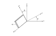
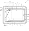
図1は、第1実施形態に係る発振器を示す断面図である。図2は、図1中の発振器を示す平面図である。図3は、ATカットのカット角を示す図である。図4は、図1の発振器の変形例を示す平面図である。なお、各図には、水晶の結晶軸であり、互いに直交するX軸、Y’軸およびZ’軸を示している。また、以下では、X軸に平行な方向を「X軸方向」とも言い、Y’軸に平行な方向を「Y’軸方向」とも言い、Z’軸に平行な方向を「Z’軸方向」とも言う。また、各軸の矢印先端側を「プラス側」とも言い、反対側を「マイナス側」とも言う。また、Y’軸方向からの平面視を単に「平面視」とも言う。
<First Embodiment>
FIG. 1 is a cross-sectional view showing an oscillator according to the first embodiment. FIG. 2 is a plan view showing the oscillator in FIG. FIG. 3 is a diagram showing a cut angle of the AT cut. FIG. 4 is a plan view showing a modified example of the oscillator of FIG. In each figure, the crystal axes of quartz are shown, and the X-axis, Y'axis, and Z'axis that are orthogonal to each other are shown. Further, in the following, the direction parallel to the X axis is also referred to as "X axis direction", the direction parallel to the Y'axis is also referred to as "Y'axis direction", and the direction parallel to the Z'axis is referred to as "Z'axis direction". Also called. Further, the tip side of the arrow of each axis is also referred to as "plus side", and the opposite side is also referred to as "minus side". Further, the plan view from the Y'axis direction is also simply referred to as "plan view".
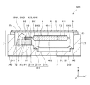
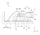
図1に示すように、発振器1は、温度補償型水晶発振器(TCXO)であり、パッケージ2と、パッケージ2に収納されている中間基板3、振動素子4および回路素子5と、を有する。発振器1は、振動デバイス10を適用したものであり、振動デバイス10は、パッケージ2、中間基板3および振動素子4から構成されている。ただし、発振器1としては、温度補償型水晶発振器に限定されない。
As shown in FIG. 1, the
パッケージ2は、上面に開口する凹部211を備えるベース21と、凹部211の開口を塞ぐようにベース21の上面に接合部材23を介して接合されているリッド22と、を有する。パッケージ2の内側には凹部211によって内部空間Sが形成され、内部空間Sに中間基板3、振動素子4および回路素子5が収納されている。例えば、ベース21は、アルミナ等のセラミックスで構成することができ、リッド22は、コバール等の金属材料で構成することができる。ただし、ベース21およびリッド22の構成材料としては、それぞれ、特に限定されない。
The
また、内部空間Sは、気密であり、減圧状態、好ましくは、より真空に近い状態となっている。これにより、振動素子4の振動特性が向上する。ただし、内部空間Sの雰囲気は、特に限定されず、例えば、窒素またはAr等の不活性ガスを封入した雰囲気であってもよく、減圧状態でなく大気圧状態または加圧状態となっていてもよい。 Further, the internal space S is airtight and is in a reduced pressure state, preferably in a state closer to vacuum. As a result, the vibration characteristics of the vibrating element 4 are improved. However, the atmosphere of the internal space S is not particularly limited, and may be, for example, an atmosphere in which an inert gas such as nitrogen or Ar is sealed, and may be in an atmospheric pressure state or a pressurized state instead of a reduced pressure state. Good.
また、凹部211は、ベース21の上面に開口している凹部211aと、凹部211aの底面に開口し、凹部211aよりも開口幅が小さい凹部211bと、凹部211bの底面に開口し、凹部211bよりも開口幅が小さい凹部211cと、を有する。そして、凹部211aの底面に中間基板3が第1接合部材B1を介して接合され、中間基板3の上面に振動素子4が第2接合部材B2を介して接合され、凹部211cの底面に回路素子5が接合されている。
Further, the
このように、振動素子4とベース21との間に中間基板3を介在させることにより、例えば、衝撃やパッケージ2の熱撓み等により生じる応力(以下、単に「パッケージ2からの応力」とも言う。)が振動素子4に伝わり難くなり、振動素子4の振動特性の低下や変動を抑制することができる。
By interposing the
第1、第2接合部材B1、B2は、機械的な接合を目的とし、電気的な接続を目的としていない。そのため、第1、第2接合部材B1、B2は、導電性であっても絶縁性であってもよい。導電性の接合部材としては、例えば、金バンプ、銀バンプ、銅バンプ、はんだバンプ等の各種金属バンプ、ポリイミド系、エポキシ系、シリコーン系、アクリル系の各種接着剤に銀フィラー等の導電性フィラーを分散させた導電性接着剤等を用いることができる。一方、絶縁性の接合部材としては、例えば、ポリイミド系、エポキシ系、シリコーン系、アクリル系の各種樹脂系の接着剤を用いることができる。なお、第1、第2接合部材B1、B2は、同種であってもよいし、異種であってもよい。 The first and second joining members B1 and B2 are intended for mechanical joining and not for electrical connection. Therefore, the first and second joining members B1 and B2 may be conductive or insulating. Examples of the conductive joining member include various metal bumps such as gold bumps, silver bumps, copper bumps, and solder bumps, various polyimide-based, epoxy-based, silicone-based, and acrylic-based adhesives, and conductive fillers such as silver filler. A conductive adhesive or the like in which the above is dispersed can be used. On the other hand, as the insulating joining member, for example, various resin-based adhesives such as polyimide-based, epoxy-based, silicone-based, and acrylic-based can be used. The first and second joining members B1 and B2 may be of the same type or different types.
また、図2に示すように、平面視で、第2接合部材B2は、第1接合部材B1と重なっている。第2接合部材B2を第1接合部材B1に重ねて配置することにより、振動素子4を中間基板3に精度よく接合することができる。具体的には、例えば、中間基板3の上面に配置した第2接合部材B2に所定の力で振動素子4を押し付けることにより、当該振動素子4を中間基板3に接合することができる。第2接合部材B2を第1接合部材B1と重ねて配置することにより、第2接合部材B2が、中間基板3、第1接合部材B1およびベース21の積層体からなる隙間のない構造体によって下方から支持された状態となるため、振動素子4の第2接合部材B2への押し付け力が逃げ難い。そのため、振動素子4を所定の力で第2接合部材B2に押し付けることができ、振動素子4を所望の接合強度でかつ所望の姿勢で中間基板3に接合することができる。したがって、振動素子4を中間基板3に精度よく接合することができる。
Further, as shown in FIG. 2, the second joining member B2 overlaps with the first joining member B1 in a plan view. By arranging the second joining member B2 so as to overlap the first joining member B1, the vibrating element 4 can be accurately joined to the
特に、本実施形態では、平面視で、第2接合部材B2の全域が第1接合部材B1と重なっている。そのため、前述した効果をより顕著に発揮することができる。ただし、これに限定されず、例えば、平面視で、第2接合部材B2の一部だけが、第1接合部材B1と重なっていてもよいし、全部が第1接合部材B1と重なっていなくてもよい。 In particular, in the present embodiment, the entire area of the second joining member B2 overlaps with the first joining member B1 in a plan view. Therefore, the above-mentioned effect can be exhibited more remarkably. However, the present invention is not limited to this, and for example, in a plan view, only a part of the second joining member B2 may overlap with the first joining member B1, and not all of them may overlap with the first joining member B1. May be good.
また、図1に示すように、凹部211aの底面には複数の内部端子241が配置されており、凹部211bの底面には複数の内部端子242が配置されており、ベース21の下面には外部端子243が配置されている。本実施形態では、第1ベース端子に相当する内部端子241Aと、第2ベース端子に相当する内部端子241Bの2つの内部端子241を有する。また、各内部端子241、242および外部端子243は、ベース21内に形成されている図示しない内部配線を介して電気的に接続されている。また、各内部端子241A、241Bは、それぞれ、第1、第2ボンディングワイヤーBW1、BW2を介して振動素子4の第1、第2端子423、424と電気的に接続され、各内部端子242は、第3ボンディングワイヤーBW3を介して回路素子5と電気的に接続されている。
Further, as shown in FIG. 1, a plurality of
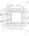
図2に示すように、振動素子4は、ATカットの素子基板41と、素子基板41の表面に配置された電極42と、を有する。素子基板41は、厚みすべり振動モードを有し、三次の周波数温度特性を有している。そのため、優れた温度特性を有する振動素子4が得られる。
As shown in FIG. 2, the vibrating element 4 has an AT-
ここで、ATカットの素子基板41について簡単に説明すると、素子基板41は、互いに直交する結晶軸X、Y、Zを有する。X軸、Y軸、Z軸は、それぞれ、電気軸、機械軸、光学軸と呼ばれる。図3に示すように、素子基板41は、X−Z面をX軸回りに所定の角度θ回転させた平面に沿って切り出された「回転Yカット水晶基板」であり、θ=35°15’回転させた平面に沿って切り出した基板を「ATカット水晶基板」という。なお、以下では、角度θに対応してX軸まわりに回転したY軸およびZ軸をY’軸およびZ’軸とする。すなわち、素子基板41は、Y’軸方向に厚みを有し、X−Z’面方向に広がりを有する。
Here, the AT-
図2に示すように、素子基板41の外形は、Y’軸方向からの平面視で矩形である。特に、本実施形態では、素子基板41は、X軸方向を長辺とし、Z’軸方向を短辺とする長手形である。また、素子基板41は、メサ型をなしており、図1に示すように、厚みすべり振動する振動部411と、振動部411の周囲に位置し、振動部411よりも厚さが薄い支持部412と、を有する。また、振動部411は、支持部412に対してY’軸方向の両側に突出している。
As shown in FIG. 2, the outer shape of the
ただし、素子基板41は、これに限定されず、振動部411と支持部412とが同じ厚さであるフラット型であってもよいし、振動部411が支持部412よりも薄い逆メサ型であってもよい。また、素子基板41の周囲を研削して面取りするベベル加工や、上面および下面を凸曲面とするコンベックス加工が施されていてもよい。また、メサ型の場合には、下面側および上面側の一方にだけ突出している構成であってもよいし、逆メサ型の場合には、下面側および上面側の一方にだけ凹没している構成であってもよい。また、素子基板41は、ATカット水晶基板に限定されず、他のカット角、例えば、Zカット、SCカット、STカット、BTカット等の水晶基板であってもよい。
However, the
また、素子基板41の構成材料は、水晶に限定されず、例えば、ニオブ酸リチウム(LiNbO3)、タンタル酸リチウム(LiTaO3)、チタン酸ジルコン酸鉛(PZT)、四ホウ酸リチウム(Li2B4O7)、ランガサイト(La3Ga5SiO14)、ニオブ酸カリウム(KNbO3)、リン酸ガリウム(GaPO4)、ガリウム砒素(GaAs)、窒化アルミニウム(AlN)、酸化亜鉛(ZnO、Zn2O3)、チタン酸バリウム(BaTiO3)、チタン酸鉛(PbPO3)、ニオブ酸ナトリウムカリウム((K,Na)NbO3)、ビスマスフェライト(BiFeO3)、ニオブ酸ナトリウム(NaNbO3)、チタン酸ビスマス(Bi4Ti3O12)、チタン酸ビスマスナトリウム(Na0.5Bi0.5TiO3)等の各種圧電材料であってもよいし、シリコン等の圧電材料以外の材料であってもよい。
The constituent material of the
図2に示すように、電極42は、振動部411の上面に配置されている第1励振電極421と、振動部411の下面に配置され、振動部411を間に挟んで第1励振電極421と対向する第2励振電極422と、を有する。また、電極42は、支持部412の上面に配置されている第1端子423および第2端子424と、第1励振電極421と第1端子423とを接続する第1引き出し配線425と、第2励振電極422と第2端子424とを接続する第2引き出し配線426と、を有する。
As shown in FIG. 2, the
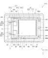
このような振動素子4は、図1および図2に示すように、支持部412のX軸方向マイナス側の端部において第2接合部材B2を介して中間基板3の上面に接合されている。特に、第2接合部材B2は、平面視で、素子基板41のZ’軸方向の中央部と重なっているため、振動素子4を安定した姿勢で中間基板3に接合することができる。なお、第2接合部材B2の構成としては、特に限定されず、例えば、図4に示すように、2つの第2接合部材B2によって振動素子4を中間基板3に接合してもよい。特に、図4に示す構成では、2つの第2接合部材B2が振動素子4のX軸方向マイナス側に位置する両角部に配置されているため、振動素子4の輪郭振動モードと呼ばれる不要振動を効果的に抑制することができる。そのため、振動漏れが減り、その分、振動素子4の振動特性が向上する。
As shown in FIGS. 1 and 2, such a vibrating element 4 is joined to the upper surface of the
また、図2に示すように、第1端子423は、第1ボンディングワイヤーBW1(第1ワイヤー)を介して内部端子241A(第1ベース端子)と電気的に接続されており、第2端子424は、第2ボンディングワイヤーBW2(第2ワイヤー)を介して別の内部端子241B(第2ベース端子)と電気的に接続されている。このように、内部端子241A、241Bと振動素子4との電気的な接続を第1、第2ボンディングワイヤーBW1、BW2を用いて行うことにより、これらの電気的な接続状態が安定し、振動素子4の振動特性が安定する。
Further, as shown in FIG. 2, the
また、平面視で、第1ボンディングワイヤーBW1が第1端子423に接続されている箇所P1は、第2接合部材B2と重なっており、第2ボンディングワイヤーBW2が第2端子424に接続されている箇所P2も、第2接合部材B2と重なっている。これら箇所P1、P2は、第2接合部材B2、中間基板3、第1接合部材B1およびベース21の積層体からなる隙間のない構造体によって下方から支持された状態となっている。
Further, in a plan view, the portion P1 where the first bonding wire BW1 is connected to the
そのため、第1、第2ボンディングワイヤーBW1、BW2を第1、第2端子423、424に接続する際に、キャピラリーを十分な力で第1、第2端子423、424に押し付けることができると共に、キャピラリーから第1、第2端子423、424に超音波を効果的に印加することができる。そのため、第1、第2ボンディングワイヤーBW1、BW2と第1、第2端子423、424との接合強度の低下を抑制することができ、振動素子4の電気的な接続状態がさらに安定する。そのため、振動素子4の振動特性がさらに安定する。
Therefore, when connecting the first and second bonding wires BW1 and BW2 to the first and
ただし、これに限定されず、箇所P1、P2の少なくとも一方は、平面視で、第2接合部材B2と重なっていなくてもよい。 However, the present invention is not limited to this, and at least one of the locations P1 and P2 may not overlap with the second joining member B2 in a plan view.
中間基板3は、ベース21と振動素子4との間に介在している。中間基板3は、パッケージ2からの応力を吸収、緩和し、当該応力を振動素子4に伝わり難くする機能を有する。図1に示すように、中間基板3は、板状であり、その下面が第1接合部材B1を介して凹部211aの底面に接合されている。そして、中間基板3の上面に第2接合部材B2を介して振動素子4が接合されている。
The
このような中間基板3は、素子基板41と同じ材料で構成されている。つまり、本実施形態では、中間基板3は、水晶で構成されている。中間基板3を振動素子4と同じ水晶で構成することにより、中間基板3と振動素子4の熱膨張係数を等しくすることができる。そのため、中間基板3と振動素子4との間には、互いの熱膨張係数差に起因する熱応力が実質的に生じず、振動素子4が応力をより受け難くなる。そのため、振動素子4の振動特性の低下や変動をより効果的に抑制することができる。
Such an
特に、中間基板3は、素子基板41と同じカット角の水晶基板から形成されている。前述したように、素子基板41は、ATカット水晶基板から形成されているため、中間基板3もATカット水晶基板から形成されている。さらに、中間基板3の結晶軸は、素子基板41の結晶軸に沿っている。具体的には、中間基板3の結晶軸のX軸が素子基板41の結晶軸のX軸に沿っており、中間基板3の結晶軸のY軸が素子基板41の結晶軸のY軸に沿っており、中間基板3の結晶軸のZ軸が素子基板41の結晶軸のZ軸に沿っている。水晶は、X軸方向、Y軸方向およびZ軸方向のそれぞれで熱膨張係数が異なるため、中間基板3と素子基板41とを同じカット角とし、互いの結晶軸の向きを揃えることにより、中間基板3と素子基板41との間で前述の熱応力がより生じ難くなる。そのため、振動素子4がさらに応力を受け難くなり、その振動特性の低下や変動をさらに効果的に抑制することができる。
In particular, the
中間基板3の厚さは、特に限定されないが、中間基板3の厚さをT2とし、振動素子4の振動部411の厚さをT3とし、支持部412の厚さをT1としたとき、T2≧T1であり、さらに、T2≧T3である。このような関係とすることにより、中間基板3を十分に厚くすることができ、前述したパッケージ2からの応力の緩和吸収効果をより顕著に発揮することができる。なお、厚さT2の上限としては、特に限定されないが、例えば、過度な厚肉化を抑制する観点から、T2/T3≦3.0であることが好ましく、T2/T3≦2.5であることがより好ましく、T2/T3≦2.0であることがさらに好ましい。なお、中間基板3の厚さT2は、より具体的には、中間基板3の第2接合部材B2と接合している部分の平均厚さのことを言い、支持部412の厚さT1は、より具体的には、支持部412の第2接合部材B2と接合している部分の平均厚さのことを言う。
The thickness of the
ただし、中間基板3としては、これに限定されず、例えば、素子基板41と同じカット角であるが、結晶軸の方向が素子基板41とは異なっていてもよい。また、中間基板3は、素子基板41と異なるカット角の水晶板から形成されていてもよい。また、中間基板3の構成材料は、水晶でなくてもよい。また、中間基板3の構成材料は、素子基板41の構成材料と異なっていてもよい。また、厚さT2は、T2<T1であってもよい。
However, the
回路素子5は、温度センサー51と、発振回路52と、を有する。発振回路52は、振動素子4を発振させ、温度センサー51の検出温度に基づいて温度補償された発振信号を生成する機能を有する。つまり、発振回路52は、振動素子4と電気的に接続され、振動素子4の出力信号を増幅し、増幅した信号を振動素子4にフィードバックすることにより振動素子4を発振させる発振回路部と、温度センサー51から出力される温度情報に基づいて、出力信号の周波数変動が振動素子4の周波数温度特性よりも小さくなるように温度補償する温度補償回路部と、を有する。なお、発振回路52としては、例えば、ピアース発振回路、インバーター型発振回路、コルピッツ発振回路、ハートレー発振回路等の発振回路を用いることができる。 The circuit element 5 includes a temperature sensor 51 and an oscillation circuit 52. The oscillation circuit 52 has a function of oscillating the vibrating element 4 and generating a temperature-compensated oscillation signal based on the temperature detected by the temperature sensor 51. That is, the oscillation circuit 52 is electrically connected to the vibrating element 4, amplifies the output signal of the vibrating element 4, and feeds back the amplified signal to the vibrating element 4 to oscillate the vibrating element 4. It includes a temperature compensation circuit unit that compensates the temperature so that the frequency fluctuation of the output signal becomes smaller than the frequency temperature characteristic of the oscillating element 4 based on the temperature information output from the temperature sensor 51. As the oscillation circuit 52, for example, an oscillation circuit such as a Pierce oscillation circuit, an inverter type oscillation circuit, a Colpitts oscillation circuit, or a Hartley oscillation circuit can be used.
以上、発振器1について説明した。このような発振器1に適用されている振動デバイス10は、前述したように、第1ベース端子および第2ベース端子としての2つの内部端子241A、241Bを含むベース21と、第1接合部材B1と、ベース21に第1接合部材B1を介して接合されている中間基板3と、第2接合部材B2と、素子基板41、素子基板41の第1面である上面に配置されている第1励振電極421、素子基板41の上面と反対の第2面である下面に配置されている第2励振電極422、第1励振電極421と接続されている第1端子423および第2励振電極422と接続されている第2端子424を含み、中間基板3に第2接合部材B2を介して接合されている振動素子4と、を備える。そして、第1端子423と一方の内部端子241Aとが第1ワイヤーとしての第1ボンディングワイヤーBW1により接続され、第2端子424と他方の内部端子241Bとが第2ワイヤーとしての第2ボンディングワイヤーBW2により接続されている。
The
このように、ベース21と振動素子4との間に中間基板3を介在させることにより、中間基板3がパッケージ2からの応力を吸収、緩和し、当該応力が振動素子4に伝わり難くなる。そのため、温度特性のヒステリシスが小さくなり、振動素子4の振動特性が安定する。特に、本実施形態では、振動素子4が1つの第2接合部材B2によって、片持ち支持、特に一点支持されているため、振動素子4に応力がより伝わり難く、振動素子4の振動特性がさらに安定する。このような効果に加えて、ベース21と振動素子4とを第1、第2ボンディングワイヤーBW1、BW2によって電気的に接続することにより、これらの電気的な接続状態が安定し、振動素子の振動特性が安定する。したがって、優れた振動特性を安定して発揮することのできる振動デバイス10となる。
By interposing the
また、前述したように、中間基板3および素子基板41は、それぞれ、水晶により構成されている。このように、中間基板3と素子基板41とを同じ材料から構成することにより、中間基板3と素子基板41の熱膨張係数を等しくすることができる。そのため、中間基板3と素子基板41との間には、互いの熱膨張係数差に起因する熱応力が実質的に生じず、振動素子4が応力をより受け難くなる。そのため、振動素子4の振動特性の低下や変動をより効果的に抑制することができる。
Further, as described above, the
また、前述したように、中間基板3の結晶軸は、素子基板41の結晶軸に沿っている。水晶は、X軸方向、Y軸方向およびZ軸方向のそれぞれで熱膨張係数が異なるため、中間基板3と素子基板41とを同じカット角とし、互いの結晶軸の向きを揃えることにより、中間基板3と素子基板41との間で前述の熱応力がより生じ難くなる。そのため、振動素子4がさらに応力を受け難くなり、その振動特性の低下や変動をさらに効果的に抑制することができる。
Further, as described above, the crystal axis of the
また、前述したように、素子基板41は、ATカット水晶基板により構成されている。ATカット水晶基板は、厚みすべり振動モードを有し、三次の周波数温度特性を有している。そのため、素子基板41をATカット水晶基板とすることにより、優れた温度特性を有する振動素子4となる。
Further, as described above, the
また、前述したように、平面視で、第1ボンディングワイヤーBW1が第1端子423に接続されている箇所P1は、第2接合部材B2と重なっており、平面視で、第2ボンディングワイヤーBW2が第2端子424に接続されている箇所P2は、第2接合部材B2と重なっている。これにより、第1、第2ボンディングワイヤーBW1、BW2を第1、第2端子423、424に接続する際に、キャピラリーを十分な力で第1、第2端子423、424に押し付けることができると共に、キャピラリーから第1、第2端子423、424に超音波を効果的に印加することができる。そのため、第1、第2ボンディングワイヤーBW1、BW2と第1、第2端子423、424との接合強度の低下を抑制することができ、振動素子4の電気的な接続状態がさらに安定する。
Further, as described above, the portion P1 in which the first bonding wire BW1 is connected to the
また、前述したように、平面視で、第2接合部材B2は、第1接合部材B1と重なっている。これにより、第2接合部材B2が第1接合部材B1によって下方から支持され、振動素子4を所定の力で第2接合部材B2に押し付けることができ、振動素子4を所望の接合強度でかつ所望の姿勢で中間基板3に接合することができる。したがって、振動素子4を中間基板3に精度よく接合することができる。
Further, as described above, the second joining member B2 overlaps with the first joining member B1 in a plan view. As a result, the second joining member B2 is supported from below by the first joining member B1, the vibrating element 4 can be pressed against the second joining member B2 with a predetermined force, and the vibrating element 4 can be pressed with a desired joining strength and desired. It can be joined to the
また、前述したように、素子基板41の第2接合部材B2と接合されている部分である支持部412の厚さをT1とし、中間基板3の第2接合部材B2と接合されている部分の厚さをT2としたとき、T2≧T1である。さらに、素子基板41の第1励振電極421と第2励振電極422とに挟まれている部分である振動部411の厚さをT3としたとき、T2≧T3である。このような関係とすることにより、中間基板3を十分に厚くすることができ、パッケージ2からの応力の緩和吸収効果をより顕著に発揮することができる。
Further, as described above, the thickness of the
また、前述したように、発振器1は、振動デバイス10と、振動素子4と電気的に接続され、発振信号を出力する発振回路52と、を備えている。そのため、発振器1は、上述した振動デバイス10の効果を享受でき、高い信頼性を発揮することができる。
Further, as described above, the
<第2実施形態>
図5は、第2実施形態に係る発振器の平面図である。
<Second Embodiment>
FIG. 5 is a plan view of the oscillator according to the second embodiment.
本実施形態に係る発振器1は、振動素子4の構成が異なること以外は、前述した第1実施形態の発振器1と同様である。なお、以下の説明では、第2実施形態の発振器1に関し、前述した第1実施形態との相違点を中心に説明し、同様の事項に関しては、その説明を省略する。また、図5では、前述した実施形態と同様の構成について、同一符号を付している。
The
図5に示す振動素子4が有する素子基板41は、前述した第1実施形態と同様にATカット水晶基板から構成されている。また、素子基板41は、平面視形状が矩形であり、X軸方向に沿う2つの辺41a、41bを有する。そして、本実施形態では、第1端子423および第2端子424は、辺41aに沿って並んで配置されている。また、平面視で、振動部411をX軸方向に延長した領域を領域Q1としたとき、第2接合部材B2は、領域Q1の外側に位置し、領域Q1の外側において、振動素子4と中間基板3とを接合している。また、平面視で、第2接合部材B2は、箇所P1、P2と重なっている。
The
ここで、振動部411ではX軸方向に沿った厚み滑り振動が生じるため、振動素子4を、領域Q1内において第2接合部材B2を介して中間基板3に接合すると、例えば、振動素子4のCI(クリスタルインピーダンス)値が増加し、振動特性に影響を与えるおそれがある。そこで、本実施形態では、第2接合部材B2を領域Q1の外側に配置することにより、このような問題の発生を抑制している。
Here, since the vibrating
以上のように、本実施形態では、素子基板41は、ATカット水晶基板により構成され、水晶の結晶軸であるX軸方向に沿う辺41a、41bを有する。そして、第1端子423および第2端子424は、辺41aに沿って並んで配置されている。第1、第2端子423、424をこのような配置することにより、平面視で、第2接合部材B2を領域Q1の外側に位置させ易くなる。そのため、上述したような振動素子4のCI(クリスタルインピーダンス)値の増加が抑制され、安定した振動特性を発揮することのできる振動素子4となる。
As described above, in the present embodiment, the
以上のような第2実施形態によっても、前述した第1実施形態と同様の効果を発揮することができる。 The second embodiment as described above can also exert the same effect as the first embodiment described above.
<第3実施形態>
図6は、第3実施形態に係る発振器の部分拡大断面図である。
<Third Embodiment>
FIG. 6 is a partially enlarged cross-sectional view of the oscillator according to the third embodiment.
本実施形態に係る発振器1は、中間基板3の構成が異なること以外は、前述した第1実施形態の発振器1と同様である。なお、以下の説明では、第3実施形態の発振器1に関し、前述した第1実施形態との相違点を中心に説明し、同様の事項に関してはその説明を省略する。また、図6では、前述した実施形態と同様の構成について、同一符号を付している。
The
図6に示すように、本実施形態の振動素子4は、前述した第1実施形態と同様にメサ型となっている。すなわち、振動部411の厚さT3が支持部412の厚さT1よりも厚くなっている。また、中間基板3は、平面視で、支持部412のみならず、振動部411とも重なって配置されている。これにより、例えば、前述した第1実施形態と比べて第1接合部材B1の塗布面積が増え、ベース21と中間基板3との接合強度が増す。また、中間基板3は、平面視で振動部411と重なる部分に切り欠きを有する。そのため、中間基板3の上面31は、支持部412と重なり、第2接合部材B2を介して振動素子4が接合されている第1面311と、振動部411と重なり、第1面311よりも下方に位置する第2面312と、を有する。このように、第2面312を第1面311よりも下方にずらすことにより、上面31と振動部411との間に十分な隙間を確保することができ、振動素子4と中間基板3との接触を効果的に抑制することができる。
As shown in FIG. 6, the vibrating element 4 of the present embodiment has a mesa type as in the first embodiment described above. That is, the thickness T3 of the vibrating
以上のように、本実施形態では、素子基板41の第2接合部材B2と接合されている第1部分である支持部412の厚さをT1とし、素子基板41の第1励振電極421と第2励振電極422とに挟まれている第2部分である振動部411の厚さをT3としたとき、T3>T1である。また、中間基板3の振動素子4側の面である上面31は、平面視で、支持部412と重なっている第1面311と、振動部411と重なり、第1面311に対して下側すなわち振動素子4とは反対側に位置する第2面312と、を有する。これにより、中間基板3と振動素子4との接触を抑制しつつ、中間基板3とベース21との接合強度を高めることができる。
As described above, in the present embodiment, the thickness of the
以上のような第3実施形態によっても、前述した第1実施形態と同様の効果を発揮することができる。 The third embodiment as described above can also exert the same effect as the first embodiment described above.
<第4実施形態>
図7は、第4実施形態に係るパーソナルコンピューターを示す斜視図である。
<Fourth Embodiment>
FIG. 7 is a perspective view showing a personal computer according to the fourth embodiment.
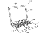
図7に示す電子機器としてのパーソナルコンピューター1100は、キーボード1102を備えた本体部1104と、表示部1108を備えた表示ユニット1106とにより構成され、表示ユニット1106は、本体部1104に対しヒンジ構造部を介して回動可能に支持されている。このようなパーソナルコンピューター1100には、発振器1が内蔵されている。また、パーソナルコンピューター1100は、キーボード1102や表示部1108などの制御に関する演算処理を行う演算処理回路1110を備えている。演算処理回路1110は、発振器1から出力される発振信号に基づいて動作する。
The
このように、電子機器としてのパーソナルコンピューター1100は、発振器1と、発振器1から出力される発振信号に基づいて動作する演算処理回路1110と、を備える。そのため、前述した発振器1の効果を享受でき、高い信頼性を発揮することができる。
As described above, the
<第5実施形態>
図8は、第5実施形態に係る携帯電話機を示す斜視図である。
<Fifth Embodiment>
FIG. 8 is a perspective view showing the mobile phone according to the fifth embodiment.
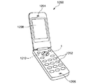
図8に示す電子機器としての携帯電話機1200は、図示しないアンテナ、複数の操作ボタン1202、受話口1204および送話口1206を備え、操作ボタン1202と受話口1204との間には表示部1208が配置されている。このような携帯電話機1200には、発振器1が内蔵されている。また、携帯電話機1200は、操作ボタン1202などの制御に関する演算処理を行う演算処理回路1210を備えている。演算処理回路1210は、発振器1から出力される発振信号に基づいて動作する。
The
このように、電子機器としての携帯電話機1200は、発振器1と、発振器1から出力される発振信号に基づいて動作する演算処理回路1210と、を備える。そのため、前述した発振器1の効果を享受でき、高い信頼性を発揮することができる。
As described above, the
<第6実施形態>
図9は、第6実施形態に係るデジタルスチールカメラを示す斜視図である。
<Sixth Embodiment>
FIG. 9 is a perspective view showing a digital still camera according to a sixth embodiment.
図9に示すデジタルスチールカメラ1300は、ボディ1302を有し、ボディ1302の背面にはCCDによる撮像信号に基づいて表示を行う表示部1310が設けられている。表示部1310は、被写体を電子画像として表示するファインダーとして機能する。また、ボディ1302の正面側(図中裏面側)には、光学レンズやCCDなどを含む受光ユニット1304が設けられている。そして、撮影者が表示部1310に表示された被写体像を確認し、シャッターボタン1306を押すと、その時点におけるCCDの撮像信号が、メモリー1308に転送・格納される。このようなデジタルスチールカメラ1300には、例えば、発振器1が内蔵されている。また、デジタルスチールカメラ1300は、表示部1310や受光ユニット1304などの制御に関する演算処理を行う演算処理回路1312を備えている。演算処理回路1312は、発振器1から出力される発振信号に基づいて動作する。
The
このように、電子機器としてのデジタルスチールカメラ1300は、発振器1と、発振器1から出力される発振信号に基づいて動作する演算処理回路1312と、を備える。そのため、前述した発振器1の効果を享受でき、高い信頼性を発揮することができる。
As described above, the
なお、本適用例の電子機器は、前述したパーソナルコンピューター、携帯電話機およびデジタルスチールカメラの他にも、例えば、スマートフォン、タブレット端末、時計(スマートウォッチを含む)、インクジェット式吐出装置(例えばインクジェットプリンタ)、ラップトップ型パーソナルコンピューター、テレビ、HMD(ヘッドマウントディスプレイ)等のウェアラブル端末、ビデオカメラ、ビデオテープレコーダー、カーナビゲーション装置、ページャ、電子手帳(通信機能付も含む)、電子辞書、電卓、電子ゲーム機器、ワードプロセッサー、ワークステーション、テレビ電話、防犯用テレビモニター、電子双眼鏡、POS端末、医療機器(例えば電子体温計、血圧計、血糖計、心電図計測装置、超音波診断装置、電子内視鏡)、魚群探知機、各種測定機器、移動体端末基地局用機器、計器類(例えば、車両、航空機、船舶の計器類)、フライトシミュレーター、ネットワークサーバー等に適用することができる。 In addition to the personal computers, mobile phones, and digital still cameras described above, the electronic devices of this application example include, for example, smartphones, tablet terminals, watches (including smart watches), and inkjet ejection devices (for example, inkjet printers). , Laptop personal computer, TV, wearable terminals such as HMD (head mount display), video camera, video tape recorder, car navigation device, pager, electronic notebook (including communication function), electronic dictionary, calculator, electronic game Equipment, word processors, workstations, videophones, security TV monitors, electronic binoculars, POS terminals, medical equipment (eg electronic thermometers, blood pressure monitors, blood glucose meters, electrocardiogram measuring devices, ultrasonic diagnostic devices, electronic endoscopes), school of fish It can be applied to detectors, various measuring devices, devices for mobile terminal base stations, instruments (for example, instruments for vehicles, aircraft, ships), flight simulators, network servers, and the like.
<第7実施形態>
図10は、第7実施形態に係る自動車を示す斜視図である。
<7th Embodiment>
FIG. 10 is a perspective view showing an automobile according to the seventh embodiment.
図10に示す自動車1500には、発振器1と、発振器1から出力される発振信号に基づいて動作する演算処理回路1510が内蔵されている。そのような発振器1と演算処理回路1510は、例えば、キーレスエントリー、イモビライザー、カーナビゲーションシステム、カーエアコン、アンチロックブレーキシステム(ABS)、エアバック、タイヤ・プレッシャー・モニタリング・システム(TPMS:Tire Pressure Monitoring System)、エンジンコントロール、ハイブリッド自動車や電気自動車の電池モニター、車体姿勢制御システム等の電子制御ユニット(ECU:electronic control unit)に広く適用できる。
The
このように、移動体としての自動車1500は、発振器1と、発振器1から出力される発振信号に基づいて動作する演算処理回路1510と、を備える。そのため、前述した発振器1の効果を享受でき、高い信頼性を発揮することができる。
As described above, the
なお、移動体としては、自動車1500に限定されず、例えば、飛行機、船舶、AGV(無人搬送車)、二足歩行ロボット、ドローン等の無人飛行機等にも適用することができる。 The moving body is not limited to the 1500 automobile, and can be applied to, for example, an airplane, a ship, an AGV (automated guided vehicle), a bipedal walking robot, an unmanned aerial vehicle such as a drone, and the like.
以上、本適用例の振動デバイス、発振器、電子機器および移動体を図示の実施形態に基づいて説明したが、本適用例は、これに限定されるものではなく、各部の構成は、同様の機能を有する任意の構成のものに置換することができる。また、本適用例に、他の任意の構成物が付加されていてもよい。また、本適用例は、前記各実施形態のうちの、任意の2以上の構成を組み合わせたものであってもよい。 The vibration device, oscillator, electronic device, and moving body of this application example have been described above based on the illustrated embodiment, but this application example is not limited to this, and the configuration of each part has the same function. Can be replaced with any configuration having. Further, any other constituent may be added to this application example. In addition, this application example may be a combination of any two or more configurations of each of the above-described embodiments.
1…発振器、10…振動デバイス、2…パッケージ、21…ベース、211、211a、211b、211c…凹部、22…リッド、23…接合部材、241、241A、241B、242…内部端子、243…外部端子、3…中間基板、31…上面、311…第1面、312…第2面、4…振動素子、41…素子基板、41a、41b…辺、411…振動部、412…支持部、42…電極、421…第1励振電極、422…第2励振電極、423…第1端子、424…第2端子、425…第1引き出し配線、426…第2引き出し配線、5…回路素子、51…温度センサー、52…発振回路、1100…パーソナルコンピューター、1102…キーボード、1104…本体部、1106…表示ユニット、1108…表示部、1110…演算処理回路、1200…携帯電話機、1202…操作ボタン、1204…受話口、1206…送話口、1208…表示部、1210…演算処理回路、1300…デジタルスチールカメラ、1302…ボディ、1304…受光ユニット、1306…シャッターボタン、1308…メモリー、1310…表示部、1312…演算処理回路、1500…自動車、1510…演算処理回路、B1…第1接合部材、B2…第2接合部材、BW1…第1ボンディングワイヤー、BW2…第2ボンディングワイヤー、BW3…第3ボンディングワイヤー、P1、P2…箇所、Q1…領域、S…内部空間、X、Y、Y’、Z、Z’…結晶軸、θ…角度 1 ... Oscillator, 10 ... Vibration device, 2 ... Package, 21 ... Base, 211, 211a, 211b, 211c ... Recess, 22 ... Lid, 23 ... Joining member, 241, 241A, 241B, 242 ... Internal terminal, 243 ... External Terminals, 3 ... Intermediate substrate, 31 ... Top surface, 311 ... First surface, 312 ... Second surface, 4 ... Vibration element, 41 ... Element substrate, 41a, 41b ... Sides, 411 ... Vibration part, 412 ... Support part, 42 ... Electrode, 421 ... 1st oscillator electrode, 422 ... 2nd oscillation electrode, 423 ... 1st terminal, 424 ... 2nd terminal, 425 ... 1st lead-out wiring, 426 ... 2nd lead-out wiring, 5 ... Circuit element, 51 ... Temperature sensor, 52 ... Oscillator circuit, 1100 ... Personal computer, 1102 ... Keyboard, 1104 ... Main unit, 1106 ... Display unit, 1108 ... Display unit, 1110 ... Arithmetic processing circuit, 1200 ... Mobile phone, 1202 ... Operation button, 1204 ... Earpiece, 1206 ... Mouthpiece, 1208 ... Display, 1210 ... Arithmetic circuit, 1300 ... Digital steel camera, 1302 ... Body, 1304 ... Light receiving unit, 1306 ... Shutter button, 1308 ... Memory, 1310 ... Display, 1312 ... Arithmetic processing circuit, 1500 ... Automobile, 1510 ... Arithmetic processing circuit, B1 ... First bonding member, B2 ... Second bonding member, BW1 ... First bonding wire, BW2 ... Second bonding wire, BW3 ... Third bonding wire, P1, P2 ... location, Q1 ... region, S ... internal space, X, Y, Y', Z, Z'... crystal axis, θ ... angle
Claims (13)
第1接合部材と、
前記ベースに前記第1接合部材を介して接合されている中間基板と、
第2接合部材と、
素子基板、前記素子基板の第1面に配置されている第1励振電極、前記素子基板の第1面と反対の第2面に配置されている第2励振電極、前記第1励振電極と接続されている第1端子および前記第2励振電極と接続されている第2端子を含み、前記中間基板に前記第2接合部材を介して接合されている振動素子と、を備え、
前記第1端子と前記第1ベース端子とが第1ワイヤーにより電気的に接続され、
前記第2端子と前記第2ベース端子とが第2ワイヤーにより電気的に接続されていることを特徴とする振動デバイス。 A base including a first base terminal and a second base terminal,
With the first joining member
With the intermediate substrate bonded to the base via the first joining member,
With the second joint member
Connected to the element substrate, the first excitation electrode arranged on the first surface of the element substrate, the second excitation electrode arranged on the second surface opposite to the first surface of the element substrate, and the first excitation electrode. A vibrating element including a first terminal and a second terminal connected to the second excitation electrode, and joined to the intermediate substrate via the second joining member.
The first terminal and the first base terminal are electrically connected by a first wire, and the first terminal is electrically connected.
A vibrating device characterized in that the second terminal and the second base terminal are electrically connected by a second wire.
平面視で、前記第2ワイヤーが前記第2端子に接続されている箇所は、前記第2接合部材と重なっている請求項1ないし4のいずれか1項に記載の振動デバイス。 In a plan view, the portion where the first wire is connected to the first terminal overlaps with the second joining member.
The vibration device according to any one of claims 1 to 4, wherein the portion where the second wire is connected to the second terminal in a plan view is overlapped with the second joining member.
前記中間基板の前記第2接合部材と接合されている部分の厚さをT2としたとき、
T2≧T1である請求項1ないし6のいずれか1項に記載の振動デバイス。 The thickness of the portion of the element substrate that is joined to the second joining member is T1.
When the thickness of the portion of the intermediate substrate joined to the second joining member is T2,
The vibration device according to any one of claims 1 to 6, wherein T2 ≧ T1.
T2≧T3である請求項7に記載の振動デバイス。 When the thickness of the portion of the element substrate sandwiched between the first excitation electrode and the second excitation electrode is T3,
The vibrating device according to claim 7, wherein T2 ≥ T3.
前記第1端子および前記第2端子は、前記辺に沿って並んで配置されている請求項1ないし3のいずれか1項、または請求項5ないし8のいずれか1項に記載の振動デバイス。 The element substrate is composed of an AT-cut quartz substrate, has a side along the X-axis direction, which is the crystal axis of quartz, and has a side.
The vibration device according to any one of claims 1 to 3, or any one of claims 5 to 8, wherein the first terminal and the second terminal are arranged side by side along the side.
T3>T1であり、
前記中間基板の前記振動素子側の面は、平面視で、前記第1部分と重なっている第1面と、前記第2部分と重なり、前記第1面に対して前記振動素子とは反対側に位置する第2面と、を有する請求項1ないし9のいずれか1項に記載の振動デバイス。 The thickness of the first portion of the element substrate that is joined to the second bonding member is T1, and the thickness of the second portion sandwiched between the first excitation electrode and the second excitation electrode of the element substrate is T1. When the value is T3
T3> T1
In plan view, the surface of the intermediate substrate on the vibrating element side overlaps the first surface and the second portion, and is opposite to the vibrating element with respect to the first surface. The vibrating device according to any one of claims 1 to 9, further comprising a second surface located in.
前記振動素子と電気的に接続され、発振信号を出力する発振回路と、を備えていることを特徴とする発振器。 The vibrating device according to any one of claims 1 to 10.
An oscillator characterized by comprising an oscillation circuit that is electrically connected to the vibrating element and outputs an oscillation signal.
前記発振器から出力される発振信号に基づいて動作する演算処理回路と、を備えていることを特徴とする電子機器。 The oscillator according to claim 11 and
An electronic device including an arithmetic processing circuit that operates based on an oscillation signal output from the oscillator.
前記発振器から出力される発振信号に基づいて動作する演算処理回路と、を備えていることを特徴とする移動体。 The oscillator according to claim 11 and
A moving body including an arithmetic processing circuit that operates based on an oscillation signal output from the oscillator.
Priority Applications (1)
| Application Number | Priority Date | Filing Date | Title |
|---|---|---|---|
| JP2019057428A JP7314562B2 (en) | 2019-03-25 | 2019-03-25 | Vibration devices, oscillators, electronic devices and moving objects |
Applications Claiming Priority (1)
| Application Number | Priority Date | Filing Date | Title |
|---|---|---|---|
| JP2019057428A JP7314562B2 (en) | 2019-03-25 | 2019-03-25 | Vibration devices, oscillators, electronic devices and moving objects |
Publications (2)
| Publication Number | Publication Date |
|---|---|
| JP2020161908A true JP2020161908A (en) | 2020-10-01 |
| JP7314562B2 JP7314562B2 (en) | 2023-07-26 |
Family
ID=72639992
Family Applications (1)
| Application Number | Title | Priority Date | Filing Date |
|---|---|---|---|
| JP2019057428A Active JP7314562B2 (en) | 2019-03-25 | 2019-03-25 | Vibration devices, oscillators, electronic devices and moving objects |
Country Status (1)
| Country | Link |
|---|---|
| JP (1) | JP7314562B2 (en) |
Cited By (5)
| Publication number | Priority date | Publication date | Assignee | Title |
|---|---|---|---|---|
| CN113492282A (en) * | 2021-07-19 | 2021-10-12 | 中国第一汽车股份有限公司 | Welding positioning system based on three-axis robot |
| WO2022024880A1 (en) * | 2020-07-29 | 2022-02-03 | 京セラ株式会社 | Piezoelectric device |
| JP2023045977A (en) * | 2021-09-22 | 2023-04-03 | 株式会社大真空 | Crystal vibration device with temperature sensor |
| JP7743655B1 (en) | 2024-04-26 | 2025-09-24 | 日本電波工業株式会社 | Crystal unit with built-in temperature sensor |
| JP2025168236A (en) * | 2024-04-26 | 2025-11-07 | 日本電波工業株式会社 | crystal oscillator |
Citations (5)
| Publication number | Priority date | Publication date | Assignee | Title |
|---|---|---|---|---|
| JPS5081296A (en) * | 1973-11-16 | 1975-07-01 | ||
| JP2011229123A (en) * | 2010-03-30 | 2011-11-10 | Nippon Dempa Kogyo Co Ltd | Crystal device and method of manufacturing crystal device |
| JP2013192052A (en) * | 2012-03-14 | 2013-09-26 | Nippon Dempa Kogyo Co Ltd | Crystal device and method of manufacturing the same |
| JP2014033368A (en) * | 2012-08-03 | 2014-02-20 | Nippon Dempa Kogyo Co Ltd | Electronic component and oscillator |
| JP2017182147A (en) * | 2016-03-28 | 2017-10-05 | アルプス電気株式会社 | Handling device |
-
2019
- 2019-03-25 JP JP2019057428A patent/JP7314562B2/en active Active
Patent Citations (5)
| Publication number | Priority date | Publication date | Assignee | Title |
|---|---|---|---|---|
| JPS5081296A (en) * | 1973-11-16 | 1975-07-01 | ||
| JP2011229123A (en) * | 2010-03-30 | 2011-11-10 | Nippon Dempa Kogyo Co Ltd | Crystal device and method of manufacturing crystal device |
| JP2013192052A (en) * | 2012-03-14 | 2013-09-26 | Nippon Dempa Kogyo Co Ltd | Crystal device and method of manufacturing the same |
| JP2014033368A (en) * | 2012-08-03 | 2014-02-20 | Nippon Dempa Kogyo Co Ltd | Electronic component and oscillator |
| JP2017182147A (en) * | 2016-03-28 | 2017-10-05 | アルプス電気株式会社 | Handling device |
Cited By (12)
| Publication number | Priority date | Publication date | Assignee | Title |
|---|---|---|---|---|
| WO2022024880A1 (en) * | 2020-07-29 | 2022-02-03 | 京セラ株式会社 | Piezoelectric device |
| JP2022025452A (en) * | 2020-07-29 | 2022-02-10 | 京セラ株式会社 | Piezoelectric device |
| JP7523271B2 (en) | 2020-07-29 | 2024-07-26 | 京セラ株式会社 | Piezoelectric Devices |
| US12438478B2 (en) | 2020-07-29 | 2025-10-07 | Kyocera Corporation | Hermetically sealed piezoelectric device with integrated temperature sensor and optimized thermal characteristics |
| CN113492282A (en) * | 2021-07-19 | 2021-10-12 | 中国第一汽车股份有限公司 | Welding positioning system based on three-axis robot |
| CN113492282B (en) * | 2021-07-19 | 2022-10-25 | 中国第一汽车股份有限公司 | Welding positioning system based on three-axis robot |
| JP2023045977A (en) * | 2021-09-22 | 2023-04-03 | 株式会社大真空 | Crystal vibration device with temperature sensor |
| JP7703972B2 (en) | 2021-09-22 | 2025-07-08 | 株式会社大真空 | Crystal device with temperature sensor |
| JP7743655B1 (en) | 2024-04-26 | 2025-09-24 | 日本電波工業株式会社 | Crystal unit with built-in temperature sensor |
| JP2025168235A (en) * | 2024-04-26 | 2025-11-07 | 日本電波工業株式会社 | Crystal unit with built-in temperature sensor |
| JP2025168236A (en) * | 2024-04-26 | 2025-11-07 | 日本電波工業株式会社 | crystal oscillator |
| JP7780679B2 (en) | 2024-04-26 | 2025-12-04 | 日本電波工業株式会社 | crystal oscillator |
Also Published As
| Publication number | Publication date |
|---|---|
| JP7314562B2 (en) | 2023-07-26 |
Similar Documents
| Publication | Publication Date | Title |
|---|---|---|
| JP7314562B2 (en) | Vibration devices, oscillators, electronic devices and moving objects | |
| JP2018006809A (en) | Oscillator, electronic apparatus, and mobile body | |
| US11075613B2 (en) | Vibrator device, electronic apparatus, and vehicle | |
| US11097667B2 (en) | Vibration device, vibration module, electronic apparatus, and vehicle | |
| US10622942B2 (en) | Oscillator, electronic apparatus, and vehicle | |
| JP2023104966A (en) | Vibration devices, electronic equipment and moving objects | |
| US10720886B2 (en) | Oscillator, electronic apparatus, and vehicle | |
| US10797644B2 (en) | Oscillator, electronic apparatus, and vehicle | |
| JP7444233B2 (en) | Method of manufacturing a vibration device | |
| US10103710B2 (en) | Resonator, oscillator, electronic apparatus, and mobile object | |
| US11009351B2 (en) | Vibrator device including reduced mounting stress and frequency variation | |
| US10536112B2 (en) | Oscillator and electronic apparatus | |
| JP2015046666A (en) | Vibration element, oscillator, sensor, electronic apparatus and mobile | |
| JP2019102848A (en) | Vibration device, manufacturing method for vibration device, electronic apparatus, and movable body | |
| US11183986B2 (en) | Resonator element, resonator device, electronic apparatus, and vehicle | |
| US11653571B2 (en) | Resonance device, oscillator, resonance module, electronic device and vehicle | |
| JP2019176224A (en) | Vibrator, oscillator, electronic apparatus, and movable body | |
| JP2019114964A (en) | Vibration device, electronic apparatus, and movable body | |
| JP2020141317A (en) | Vibrating elements, vibrating devices, oscillators, electronics and moving objects |
Legal Events
| Date | Code | Title | Description |
|---|---|---|---|
| A621 | Written request for application examination |
Free format text: JAPANESE INTERMEDIATE CODE: A621 Effective date: 20220114 |
|
| A977 | Report on retrieval |
Free format text: JAPANESE INTERMEDIATE CODE: A971007 Effective date: 20221221 |
|
| A131 | Notification of reasons for refusal |
Free format text: JAPANESE INTERMEDIATE CODE: A131 Effective date: 20230117 |
|
| A521 | Request for written amendment filed |
Free format text: JAPANESE INTERMEDIATE CODE: A523 Effective date: 20230317 |
|
| TRDD | Decision of grant or rejection written | ||
| A01 | Written decision to grant a patent or to grant a registration (utility model) |
Free format text: JAPANESE INTERMEDIATE CODE: A01 Effective date: 20230613 |
|
| A61 | First payment of annual fees (during grant procedure) |
Free format text: JAPANESE INTERMEDIATE CODE: A61 Effective date: 20230626 |
|
| R150 | Certificate of patent or registration of utility model |
Ref document number: 7314562 Country of ref document: JP Free format text: JAPANESE INTERMEDIATE CODE: R150 |