JP2020161663A - Semiconductor laser device - Google Patents
Semiconductor laser device Download PDFInfo
- Publication number
- JP2020161663A JP2020161663A JP2019060074A JP2019060074A JP2020161663A JP 2020161663 A JP2020161663 A JP 2020161663A JP 2019060074 A JP2019060074 A JP 2019060074A JP 2019060074 A JP2019060074 A JP 2019060074A JP 2020161663 A JP2020161663 A JP 2020161663A
- Authority
- JP
- Japan
- Prior art keywords
- semiconductor laser
- fixed base
- laser device
- elements
- inclined surface
- Prior art date
- Legal status (The legal status is an assumption and is not a legal conclusion. Google has not performed a legal analysis and makes no representation as to the accuracy of the status listed.)
- Pending
Links
Images


Landscapes
- Semiconductor Lasers (AREA)
Abstract
【課題】半導体レーザ素子で発生する熱を効率よく放熱することができる半導体レーザ装置を提供する。【解決手段】半導体レーザ装置は、複数の半導体レーザ素子と、前記複数の半導体レーザ素子を配置する固定台と、を備える。ここで、前記固定台の上面は底面に対して傾斜面を有し、前記傾斜面に前記半導体レーザ素子が設けられる。この構成により、半導体レーザ素子で発生する熱を効率よく放熱することができる半導体レーザ装置を提供することができる。【選択図】図1PROBLEM TO BE SOLVED: To provide a semiconductor laser apparatus capable of efficiently dissipating heat generated by a semiconductor laser element. A semiconductor laser device includes a plurality of semiconductor laser elements and a fixed base on which the plurality of semiconductor laser elements are arranged. Here, the upper surface of the fixed base has an inclined surface with respect to the bottom surface, and the semiconductor laser element is provided on the inclined surface. With this configuration, it is possible to provide a semiconductor laser device capable of efficiently dissipating heat generated by the semiconductor laser element. [Selection diagram] Fig. 1
Description
本発明は、半導体レーザ装置に関する。 The present invention relates to a semiconductor laser device.
レーザ加工は、レーザ光を用いるため、従来工法と比較して非接触加工、微細加工を実現することができる。特に、半導体レーザ素子を光源として用いるダイレクトダイオードレーザ方式は、レーザ光を変換しないため高効率である。しかしながら、半導体レーザ素子の出力特性は、発光層の温度に強く依存する。高出力領域では電流供給の増加によって発光層からキャリアである電子・正孔キャリアがオーバーフローし、非発光再結合で消費されることで、発光に寄与しない無効電力が増加することで、発光層温度が上昇する。発光層温度の上昇に伴い、半導体レーザ素子の信頼性低下が生じる。 Since laser processing uses laser light, non-contact processing and fine processing can be realized as compared with the conventional method. In particular, the direct diode laser method using a semiconductor laser element as a light source is highly efficient because it does not convert the laser beam. However, the output characteristics of the semiconductor laser device strongly depend on the temperature of the light emitting layer. In the high output region, the electron / hole carriers, which are carriers, overflow from the light emitting layer due to the increase in current supply, and are consumed by non-light emission recombination, so that the ineffective power that does not contribute to light emission increases, resulting in the light emitting layer temperature. Rise. As the temperature of the light emitting layer rises, the reliability of the semiconductor laser device decreases.
しかしながら、加工用途としてレーザ光を用いるためには、数百ワット〜数キロワットの光出力が必要である。そのため、加工用途としてレーザ光を用いる場合、例えば、発光層の熱分散の観点から半導体レーザ素子には、複数のエミッタを多数並べたアレイ構造が採用される。複数のマルチエミッタ構造の半導体レーザ素子によれば、それぞれのエミッタから出力されるレーザ光を合成することで、大出力のレーザ光を得ることができる。 However, in order to use laser light for processing, an optical output of several hundred watts to several kilowatts is required. Therefore, when laser light is used for processing, for example, from the viewpoint of thermal dispersion of the light emitting layer, an array structure in which a large number of a plurality of emitters are arranged is adopted for the semiconductor laser element. According to the semiconductor laser elements having a plurality of multi-emitter structures, a high-power laser beam can be obtained by synthesizing the laser beams output from the respective emitters.
例えば、特許文献1においては、複数の半導体レーザ素子から出力されるレーザ光を合成する際、階段状の固定台に複数の半導体レーザ素子を配置し、半導体レーザ素子から出力されるレーザ光を集光レンズ用いて出力される構成になっている。
For example, in
しかしながら、特許文献1で開示されている構成では、固定台全体を冷却する必要があるため、筐体サイズが大きくなる。もしくは、固定台底部を冷却する場合、階段の最上段と最下段において冷却面である底部と半導体レーザ素子との距離が異なるため発光層温度に差が生じるため、半導体レーザ装置の信頼性低下が生じる課題があった。
However, in the configuration disclosed in
半導体レーザ装置は、複数の半導体レーザ素子と、前記複数の半導体レーザ素子を配置する固定台と、を備える。ここで、前記固定台の上面は底面に対して傾斜面を有し、前記傾斜面に前記半導体レーザ素子が設けられる。 The semiconductor laser device includes a plurality of semiconductor laser elements and a fixed base on which the plurality of semiconductor laser elements are arranged. Here, the upper surface of the fixed base has an inclined surface with respect to the bottom surface, and the semiconductor laser element is provided on the inclined surface.
本発明の半導体レーザ装置においては、半導体レーザ素子は固定台の底面に対して傾斜した複数の面上に備えられている。これにより、複数の傾斜面における半導体レーザ素子の発光層位置が冷却部である固定台底面から等距離となるため半導体レーザ素子間での発光層の温度差を抑制することができ、信頼性の高い半導体レーザ装置を提供できる。 In the semiconductor laser device of the present invention, the semiconductor laser element is provided on a plurality of surfaces inclined with respect to the bottom surface of the fixed base. As a result, the position of the light emitting layer of the semiconductor laser element on the plurality of inclined surfaces is equal to the bottom surface of the fixed table which is the cooling portion, so that the temperature difference of the light emitting layer between the semiconductor laser elements can be suppressed, and the reliability is high. An expensive semiconductor laser device can be provided.
以下、本開示の実施の形態について、図面を参照しながら説明する。なお、以下に説明する実施の形態は、いずれも本開示の一具体例を示すものである。したがって、以下の実施の形態で示される、数値、形状、材料、構成要素、構成要素の配置位置及び接続形態等は、一例であって本開示を限定する主旨ではない。よって、以下の実施の形態における構成要素のうち、本開示の最上位概念を示す独立請求項に記載されていない構成要素については、任意の構成要素として説明される。 Hereinafter, embodiments of the present disclosure will be described with reference to the drawings. It should be noted that all of the embodiments described below show a specific example of the present disclosure. Therefore, the numerical values, shapes, materials, components, the arrangement positions of the components, the connection form, and the like shown in the following embodiments are examples and are not intended to limit the present disclosure. Therefore, among the components in the following embodiments, the components not described in the independent claims indicating the highest level concept of the present disclosure will be described as arbitrary components.
各図は、模式図であり、必ずしも厳密に図示されたものではない。したがって、各図において縮尺などは必ずしも一致していない。各図において、実質的に同一の構成に対しては同一の符号を付しており、重複する説明は省略又は簡略化する。 Each figure is a schematic view and is not necessarily exactly illustrated. Therefore, the scales and the like do not always match in each figure. In each figure, substantially the same configuration is designated by the same reference numerals, and duplicate description will be omitted or simplified.
また、本明細書及び図面において、X軸、Y軸及びZ軸は、三次元直交座標系の三軸を表している。したがって、X軸及びY軸は、互いに直交し、かつ、いずれもZ軸に直交する軸である。
(実施の形態1)
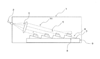
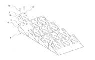
図1は、本実施の形態における半導体レーザ装置1の側面図である。図2は本実施の形態における半導体レーザ装置1の上面図であり。図3は半導体レーザ素子5の分解斜視図である。図4は半導体レーザ装置1の固定台6の斜視図である。
Further, in the present specification and drawings, the X-axis, the Y-axis, and the Z-axis represent the three axes of the three-dimensional Cartesian coordinate system. Therefore, the X-axis and the Y-axis are orthogonal to each other and both are orthogonal to the Z-axis.
(Embodiment 1)
FIG. 1 is a side view of the
半導体レーザ装置1は、図1に示すように、傾斜面7を複数有する固定台6と、固定台6の底部に設けられた冷却機構9と、傾斜面7上に固定された半導体レーザ素子5と、前記半導体レーザ素子5から出射されるレーザ光10をコリメートする図示しない光学素子と、コリメートされたビームを一点に集光する集光レンズ3、導光部2(例えば、1本の光ファイバー、1本のロッドファイバ、部分反射ミラー)を備える。
As shown in FIG. 1, the
半導体レーザ素子5は、固定台上に図示しない絶縁性を有するシート上に配置されている。また、半導体レーザ素子5は、図示しない配線によって直列で接続されている。
The
固定台6は、熱伝導性に優れた金属材料からなり、ワイヤ放電加工や切削加工によって形成する事ができる。固定台6は冷却機構9の上に設けられる。冷却機構9は、金属ブロックを用いてもよいし、内部に水冷機構を組み込まれていてもよい。
The
傾斜面7は、固定台底面8に対して規定される所定の角度を有する。所定の角度は、0度より大きく、90度より小さい。
The
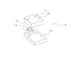
図3に示すように、半導体レーザ素子5は、例えば、熱伝導性に優れた金属材料からなる上面ブロック12と下面ブロック15によって、サブマウント14上に配置された半導体レーザチップ13を挟み込んだ形態である。
As shown in FIG. 3, the
固定穴11は、上面ブロック12、下面ブロック15、固定台6を連通する様に設けられている。この固定穴11に固定具16が挿入される事で、半導体レーザ素子5が固定台6に固定される。
The
サブマウント14は、熱伝導性に優れた材料(例えば、ダイヤモンド、シリコンカーバイト、銅ダイヤモンド、窒化アルミ、銅タングステンなど)とし、サブマウント14表面には電極パターンが形成されている。半導体レーザチップ13はサブマウント14上に半田などにより実装されている。また、傾斜面7は、前列から後列にかけてほぼ同じ傾きを有している。このため、半導体レーザ素子5は、(側面視において)互いにほぼ同じ高さに配置される。この構成により、固定台6の底面を階段状にし、この階段に半導体レーザを配置する場合と比べて、前列に配置される半導体レーザ素子5の発光層と冷却機構9の距離と後列に配置される半導体レーザ素子5の発光層と冷却機構9の距離との差が小さくなる。これにより、半導体レーザ素子5間での放熱ばらつきが低減する。結果、半導体レーザ素子5間での発光層の温度差が低減される。結果、半導体レーザ装置1の信頼性が向上する。
The
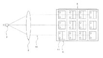
図5は、本実施の形態における半導体レーザ装置の変形例の側面図である。図6は、同変形例の上面図である。図5、6に記載の様に、集光レンズ3と半導体レーザ素子5の間に角度変換素子4(例えばプリズムや透過型の波長分散素子、あるいは反射型の波長分散素子など)を配置することで、レーザ光10を一点に集光することができる。
FIG. 5 is a side view of a modified example of the semiconductor laser device according to the present embodiment. FIG. 6 is a top view of the modified example. As shown in FIGS. 5 and 6, an angle conversion element 4 (for example, a prism, a transmission type wavelength dispersion element, or a reflection type wavelength dispersion element) is arranged between the condensing
前列と後列の半導体レーザ素子5の発振波長を変化させる(例えば前列をGaNを母材とする半導体レーザ、後列をGaAsを母材とする半導体レーザとする)ことで、角度変換素子4との組み合わせにより、複数の発振波長のレーザ光10の高密度化が可能である。
By changing the oscillation wavelengths of the
図7は、本実施の形態における半導体レーザ装置の別の変形例の上面図である。図7に記載の様に、同一列にある半導体レーザ素子5のレーザ光10の出射方向を中央の半導体レーザ素子5に対して傾斜させることで、レーザ光10の高密度化が可能である。
FIG. 7 is a top view of another modification of the semiconductor laser device according to the present embodiment. As shown in FIG. 7, the density of the
本開示に係る半導体レーザ装置は、放熱性に優れるので、プロジェクタ等に用いられる画像表示用光源、レーザ加工装置に用いられる加工用光源又は産業用スポット照明等に用いられる照明用光源等として利用することができ、特に、比較的に高い光出力を必要とする機器の光源として有用である。 Since the semiconductor laser device according to the present disclosure has excellent heat dissipation, it is used as an image display light source used for a projector or the like, a processing light source used for a laser processing device, a lighting light source used for industrial spot lighting, or the like. It can be used, and is particularly useful as a light source for equipment that requires a relatively high light output.
1 半導体レーザ装置
2 導光部
3 集光レンズ
4 角度変換素子
5 半導体レーザ素子
6 固定台
7 傾斜面
8 固定台底面
9 冷却機構
10 レーザ光
11 固定穴
12 上面ブロック
13 半導体レーザチップ
14 サブマウント
15 下面ブロック
16 固定具
1
Claims (4)
前記複数の半導体レーザ素子を配置する固定台と、を備え、
前記固定台の上面は、前記固定台の底面に対して傾斜した傾斜面を有し、前記複数の半導体レーザ素子は、前記傾斜面に設けられる、
半導体レーザ装置。 With multiple semiconductor laser devices
A fixed base on which the plurality of semiconductor laser elements are arranged is provided.
The upper surface of the fixed base has an inclined surface inclined with respect to the bottom surface of the fixed base, and the plurality of semiconductor laser elements are provided on the inclined surface.
Semiconductor laser device.
前記半導体レーザ素子が出射するレーザの出射方向に配置された、レーザの光軸を変換する光学素子と、を更に備える請求項1に記載の半導体レーザ装置。 A beam shaping optical element arranged in front of the semiconductor laser element and
The semiconductor laser device according to claim 1, further comprising an optical element for converting the optical axis of the laser, which is arranged in the emission direction of the laser emitted by the semiconductor laser element.
Priority Applications (1)
| Application Number | Priority Date | Filing Date | Title |
|---|---|---|---|
| JP2019060074A JP2020161663A (en) | 2019-03-27 | 2019-03-27 | Semiconductor laser device |
Applications Claiming Priority (1)
| Application Number | Priority Date | Filing Date | Title |
|---|---|---|---|
| JP2019060074A JP2020161663A (en) | 2019-03-27 | 2019-03-27 | Semiconductor laser device |
Publications (1)
| Publication Number | Publication Date |
|---|---|
| JP2020161663A true JP2020161663A (en) | 2020-10-01 |
Family
ID=72639859
Family Applications (1)
| Application Number | Title | Priority Date | Filing Date |
|---|---|---|---|
| JP2019060074A Pending JP2020161663A (en) | 2019-03-27 | 2019-03-27 | Semiconductor laser device |
Country Status (1)
| Country | Link |
|---|---|
| JP (1) | JP2020161663A (en) |
Cited By (1)
| Publication number | Priority date | Publication date | Assignee | Title |
|---|---|---|---|---|
| CN118281701A (en) * | 2024-05-29 | 2024-07-02 | 深圳活力激光技术有限公司 | Semiconductor laser |
-
2019
- 2019-03-27 JP JP2019060074A patent/JP2020161663A/en active Pending
Cited By (1)
| Publication number | Priority date | Publication date | Assignee | Title |
|---|---|---|---|---|
| CN118281701A (en) * | 2024-05-29 | 2024-07-02 | 深圳活力激光技术有限公司 | Semiconductor laser |
Similar Documents
| Publication | Publication Date | Title |
|---|---|---|
| US8432945B2 (en) | Laser diode combiner modules | |
| US8000360B2 (en) | Laser diode assemblies | |
| US7420996B2 (en) | Modular diode laser assembly | |
| CN113725722B (en) | Projection of patterned and flood illumination | |
| US20090129103A1 (en) | Led lamp with a heat dissipation device | |
| US20080291955A1 (en) | Modular diode laser assembly | |
| US7443895B2 (en) | Modular diode laser assembly | |
| US7586963B2 (en) | Modular diode laser assembly | |
| US20070116070A1 (en) | Modular diode laser assembly | |
| EP2908390B1 (en) | Semiconductor laser light source | |
| JP7656188B2 (en) | Semiconductor laser device | |
| US20220263293A1 (en) | Semiconductor laser and material machining method using a semiconductor laser | |
| JP3202736U (en) | Package structure for laser diode | |
| CN115377790B (en) | Double sided cooling of laser diode | |
| JP2020161663A (en) | Semiconductor laser device | |
| CN215771895U (en) | Laser device | |
| JP7050045B2 (en) | Package, light emitting device, and laser device | |
| US20080089371A1 (en) | Bright light source with two-dimensional array of diode-laser emitters | |
| US4864584A (en) | Laser diode pumped ND:YAG laser and method of making same | |
| JP7431553B2 (en) | semiconductor laser equipment | |
| JP2006013038A (en) | Semiconductor laser array device | |
| WO2020044882A1 (en) | Semiconductor laser device | |
| CN221947593U (en) | Laser modules and laser equipment | |
| RU232175U1 (en) | MULTISPECTRUM LASER MODULE | |
| CN114937914A (en) | a semiconductor laser |
Legal Events
| Date | Code | Title | Description |
|---|---|---|---|
| RD01 | Notification of change of attorney |
Free format text: JAPANESE INTERMEDIATE CODE: A7421 Effective date: 20200611 |