JP2020136282A - High-frequency circuit board manufacturing method and high-frequency circuit board - Google Patents
High-frequency circuit board manufacturing method and high-frequency circuit board Download PDFInfo
- Publication number
- JP2020136282A JP2020136282A JP2019022801A JP2019022801A JP2020136282A JP 2020136282 A JP2020136282 A JP 2020136282A JP 2019022801 A JP2019022801 A JP 2019022801A JP 2019022801 A JP2019022801 A JP 2019022801A JP 2020136282 A JP2020136282 A JP 2020136282A
- Authority
- JP
- Japan
- Prior art keywords
- dielectric layer
- frequency circuit
- layer portion
- circuit board
- cavity
- Prior art date
- Legal status (The legal status is an assumption and is not a legal conclusion. Google has not performed a legal analysis and makes no representation as to the accuracy of the status listed.)
- Granted
Links
Images


Classifications
-
- H—ELECTRICITY
- H05—ELECTRIC TECHNIQUES NOT OTHERWISE PROVIDED FOR
- H05K—PRINTED CIRCUITS; CASINGS OR CONSTRUCTIONAL DETAILS OF ELECTRIC APPARATUS; MANUFACTURE OF ASSEMBLAGES OF ELECTRICAL COMPONENTS
- H05K1/00—Printed circuits
- H05K1/02—Details
- H05K1/0213—Electrical arrangements not otherwise provided for
- H05K1/0237—High frequency adaptations
- H05K1/0243—Printed circuits associated with mounted high frequency components
-
- H—ELECTRICITY
- H01—ELECTRIC ELEMENTS
- H01Q—ANTENNAS, i.e. RADIO AERIALS
- H01Q1/00—Details of, or arrangements associated with, antennas
- H01Q1/27—Adaptation for use in or on movable bodies
- H01Q1/32—Adaptation for use in or on road or rail vehicles
- H01Q1/3208—Adaptation for use in or on road or rail vehicles characterised by the application wherein the antenna is used
- H01Q1/3233—Adaptation for use in or on road or rail vehicles characterised by the application wherein the antenna is used particular used as part of a sensor or in a security system, e.g. for automotive radar, navigation systems
-
- H—ELECTRICITY
- H01—ELECTRIC ELEMENTS
- H01Q—ANTENNAS, i.e. RADIO AERIALS
- H01Q1/00—Details of, or arrangements associated with, antennas
- H01Q1/12—Supports; Mounting means
- H01Q1/22—Supports; Mounting means by structural association with other equipment or articles
- H01Q1/2283—Supports; Mounting means by structural association with other equipment or articles mounted in or on the surface of a semiconductor substrate as a chip-type antenna or integrated with other components into an IC package
-
- H—ELECTRICITY
- H01—ELECTRIC ELEMENTS
- H01Q—ANTENNAS, i.e. RADIO AERIALS
- H01Q1/00—Details of, or arrangements associated with, antennas
- H01Q1/36—Structural form of radiating elements, e.g. cone, spiral, umbrella; Particular materials used therewith
- H01Q1/38—Structural form of radiating elements, e.g. cone, spiral, umbrella; Particular materials used therewith formed by a conductive layer on an insulating support
-
- H—ELECTRICITY
- H05—ELECTRIC TECHNIQUES NOT OTHERWISE PROVIDED FOR
- H05K—PRINTED CIRCUITS; CASINGS OR CONSTRUCTIONAL DETAILS OF ELECTRIC APPARATUS; MANUFACTURE OF ASSEMBLAGES OF ELECTRICAL COMPONENTS
- H05K1/00—Printed circuits
- H05K1/02—Details
- H05K1/0213—Electrical arrangements not otherwise provided for
- H05K1/0237—High frequency adaptations
- H05K1/024—Dielectric details, e.g. changing the dielectric material around a transmission line
-
- H—ELECTRICITY
- H05—ELECTRIC TECHNIQUES NOT OTHERWISE PROVIDED FOR
- H05K—PRINTED CIRCUITS; CASINGS OR CONSTRUCTIONAL DETAILS OF ELECTRIC APPARATUS; MANUFACTURE OF ASSEMBLAGES OF ELECTRICAL COMPONENTS
- H05K1/00—Printed circuits
- H05K1/02—Details
- H05K1/0213—Electrical arrangements not otherwise provided for
- H05K1/0237—High frequency adaptations
- H05K1/0242—Structural details of individual signal conductors, e.g. related to the skin effect
-
- H—ELECTRICITY
- H05—ELECTRIC TECHNIQUES NOT OTHERWISE PROVIDED FOR
- H05K—PRINTED CIRCUITS; CASINGS OR CONSTRUCTIONAL DETAILS OF ELECTRIC APPARATUS; MANUFACTURE OF ASSEMBLAGES OF ELECTRICAL COMPONENTS
- H05K1/00—Printed circuits
- H05K1/02—Details
- H05K1/11—Printed elements for providing electric connections to or between printed circuits
- H05K1/111—Pads for surface mounting, e.g. lay-out
-
- H—ELECTRICITY
- H05—ELECTRIC TECHNIQUES NOT OTHERWISE PROVIDED FOR
- H05K—PRINTED CIRCUITS; CASINGS OR CONSTRUCTIONAL DETAILS OF ELECTRIC APPARATUS; MANUFACTURE OF ASSEMBLAGES OF ELECTRICAL COMPONENTS
- H05K1/00—Printed circuits
- H05K1/16—Printed circuits incorporating printed electric components, e.g. printed resistors, capacitors or inductors
- H05K1/165—Printed circuits incorporating printed electric components, e.g. printed resistors, capacitors or inductors incorporating printed inductors
-
- H—ELECTRICITY
- H05—ELECTRIC TECHNIQUES NOT OTHERWISE PROVIDED FOR
- H05K—PRINTED CIRCUITS; CASINGS OR CONSTRUCTIONAL DETAILS OF ELECTRIC APPARATUS; MANUFACTURE OF ASSEMBLAGES OF ELECTRICAL COMPONENTS
- H05K1/00—Printed circuits
- H05K1/18—Printed circuits structurally associated with non-printed electric components
- H05K1/182—Printed circuits structurally associated with non-printed electric components associated with components mounted in printed circuit boards [PCB], e.g. insert-mounted components [IMC]
- H05K1/185—Printed circuits structurally associated with non-printed electric components associated with components mounted in printed circuit boards [PCB], e.g. insert-mounted components [IMC] associated with components encapsulated in the insulating substrate of the PCBs; associated with components incorporated in internal layers of multilayer circuit boards
- H05K1/186—Printed circuits structurally associated with non-printed electric components associated with components mounted in printed circuit boards [PCB], e.g. insert-mounted components [IMC] associated with components encapsulated in the insulating substrate of the PCBs; associated with components incorporated in internal layers of multilayer circuit boards manufactured by mounting on or connecting to patterned circuits before or during embedding
-
- H—ELECTRICITY
- H05—ELECTRIC TECHNIQUES NOT OTHERWISE PROVIDED FOR
- H05K—PRINTED CIRCUITS; CASINGS OR CONSTRUCTIONAL DETAILS OF ELECTRIC APPARATUS; MANUFACTURE OF ASSEMBLAGES OF ELECTRICAL COMPONENTS
- H05K3/00—Apparatus or processes for manufacturing printed circuits
- H05K3/46—Manufacturing multilayer circuits
- H05K3/4644—Manufacturing multilayer circuits by building the multilayer layer by layer, i.e. build-up multilayer circuits
- H05K3/4652—Adding a circuit layer by laminating a metal foil or a preformed metal foil pattern
-
- H—ELECTRICITY
- H05—ELECTRIC TECHNIQUES NOT OTHERWISE PROVIDED FOR
- H05K—PRINTED CIRCUITS; CASINGS OR CONSTRUCTIONAL DETAILS OF ELECTRIC APPARATUS; MANUFACTURE OF ASSEMBLAGES OF ELECTRICAL COMPONENTS
- H05K3/00—Apparatus or processes for manufacturing printed circuits
- H05K3/46—Manufacturing multilayer circuits
- H05K3/4644—Manufacturing multilayer circuits by building the multilayer layer by layer, i.e. build-up multilayer circuits
- H05K3/4682—Manufacture of core-less build-up multilayer circuits on a temporary carrier or on a metal foil
-
- H—ELECTRICITY
- H05—ELECTRIC TECHNIQUES NOT OTHERWISE PROVIDED FOR
- H05K—PRINTED CIRCUITS; CASINGS OR CONSTRUCTIONAL DETAILS OF ELECTRIC APPARATUS; MANUFACTURE OF ASSEMBLAGES OF ELECTRICAL COMPONENTS
- H05K3/00—Apparatus or processes for manufacturing printed circuits
- H05K3/46—Manufacturing multilayer circuits
- H05K3/4697—Manufacturing multilayer circuits having cavities, e.g. for mounting components
-
- H—ELECTRICITY
- H05—ELECTRIC TECHNIQUES NOT OTHERWISE PROVIDED FOR
- H05K—PRINTED CIRCUITS; CASINGS OR CONSTRUCTIONAL DETAILS OF ELECTRIC APPARATUS; MANUFACTURE OF ASSEMBLAGES OF ELECTRICAL COMPONENTS
- H05K2201/00—Indexing scheme relating to printed circuits covered by H05K1/00
- H05K2201/01—Dielectrics
- H05K2201/0104—Properties and characteristics in general
- H05K2201/0129—Thermoplastic polymer, e.g. auto-adhesive layer; Shaping of thermoplastic polymer
-
- H—ELECTRICITY
- H05—ELECTRIC TECHNIQUES NOT OTHERWISE PROVIDED FOR
- H05K—PRINTED CIRCUITS; CASINGS OR CONSTRUCTIONAL DETAILS OF ELECTRIC APPARATUS; MANUFACTURE OF ASSEMBLAGES OF ELECTRICAL COMPONENTS
- H05K2201/00—Indexing scheme relating to printed circuits covered by H05K1/00
- H05K2201/01—Dielectrics
- H05K2201/0183—Dielectric layers
- H05K2201/0187—Dielectric layers with regions of different dielectrics in the same layer, e.g. in a printed capacitor for locally changing the dielectric properties
-
- H—ELECTRICITY
- H05—ELECTRIC TECHNIQUES NOT OTHERWISE PROVIDED FOR
- H05K—PRINTED CIRCUITS; CASINGS OR CONSTRUCTIONAL DETAILS OF ELECTRIC APPARATUS; MANUFACTURE OF ASSEMBLAGES OF ELECTRICAL COMPONENTS
- H05K2201/00—Indexing scheme relating to printed circuits covered by H05K1/00
- H05K2201/01—Dielectrics
- H05K2201/0183—Dielectric layers
- H05K2201/0195—Dielectric or adhesive layers comprising a plurality of layers, e.g. in a multilayer structure
-
- H—ELECTRICITY
- H05—ELECTRIC TECHNIQUES NOT OTHERWISE PROVIDED FOR
- H05K—PRINTED CIRCUITS; CASINGS OR CONSTRUCTIONAL DETAILS OF ELECTRIC APPARATUS; MANUFACTURE OF ASSEMBLAGES OF ELECTRICAL COMPONENTS
- H05K2201/00—Indexing scheme relating to printed circuits covered by H05K1/00
- H05K2201/10—Details of components or other objects attached to or integrated in a printed circuit board
- H05K2201/10007—Types of components
- H05K2201/10098—Components for radio transmission, e.g. radio frequency identification [RFID] tag, printed or non-printed antennas
-
- H—ELECTRICITY
- H05—ELECTRIC TECHNIQUES NOT OTHERWISE PROVIDED FOR
- H05K—PRINTED CIRCUITS; CASINGS OR CONSTRUCTIONAL DETAILS OF ELECTRIC APPARATUS; MANUFACTURE OF ASSEMBLAGES OF ELECTRICAL COMPONENTS
- H05K2203/00—Indexing scheme relating to apparatus or processes for manufacturing printed circuits covered by H05K3/00
- H05K2203/01—Tools for processing; Objects used during processing
- H05K2203/0147—Carriers and holders
- H05K2203/0152—Temporary metallic carrier, e.g. for transferring material
-
- H—ELECTRICITY
- H05—ELECTRIC TECHNIQUES NOT OTHERWISE PROVIDED FOR
- H05K—PRINTED CIRCUITS; CASINGS OR CONSTRUCTIONAL DETAILS OF ELECTRIC APPARATUS; MANUFACTURE OF ASSEMBLAGES OF ELECTRICAL COMPONENTS
- H05K2203/00—Indexing scheme relating to apparatus or processes for manufacturing printed circuits covered by H05K3/00
- H05K2203/11—Treatments characterised by their effect, e.g. heating, cooling, roughening
- H05K2203/1105—Heating or thermal processing not related to soldering, firing, curing or laminating, e.g. for shaping the substrate or during finish plating
-
- H—ELECTRICITY
- H10—SEMICONDUCTOR DEVICES; ELECTRIC SOLID-STATE DEVICES NOT OTHERWISE PROVIDED FOR
- H10W—GENERIC PACKAGES, INTERCONNECTIONS, CONNECTORS OR OTHER CONSTRUCTIONAL DETAILS OF DEVICES COVERED BY CLASS H10
- H10W90/00—Package configurations
- H10W90/701—Package configurations characterised by the relative positions of pads or connectors relative to package parts
- H10W90/721—Package configurations characterised by the relative positions of pads or connectors relative to package parts of bump connectors
- H10W90/724—Package configurations characterised by the relative positions of pads or connectors relative to package parts of bump connectors between a chip and a stacked insulating package substrate, interposer or RDL
Landscapes
- Engineering & Computer Science (AREA)
- Microelectronics & Electronic Packaging (AREA)
- Manufacturing & Machinery (AREA)
- Computer Security & Cryptography (AREA)
- Radar, Positioning & Navigation (AREA)
- Remote Sensing (AREA)
- Structure Of Printed Boards (AREA)
- Production Of Multi-Layered Print Wiring Board (AREA)
- Parts Printed On Printed Circuit Boards (AREA)
- Radar Systems Or Details Thereof (AREA)
Abstract
【課題】電子部品の熱破損を抑制しつつ高周波特性を向上させた小型の高周波回路基板を提供する。【解決手段】高周波回路基板1の製造方法は、仮基材11の上面にアンテナパターン3を形成する第1工程と、仮基材11の上面に熱可塑性樹脂13及び仮導体12をこの順に重ねた状態で熱プレスし、熱可塑性樹脂13からアンテナパターン3を覆う第1誘電体層部6を成形する第2工程と、仮導体12を除去した後に第1誘電体層6に削り出し加工を施して、電子部品4を収容可能なキャビティ6aを形成する第3工程と、キャビティ6a内において電子部品4をアンテナパターン3に実装する第4工程と、第1誘電体層部6におけるキャビティ6aの開口側に熱硬化性樹脂14及びグランド導体2をこの順に重ねた状態で熱プレスし、熱硬化性樹脂14からキャビティ6a内の電子部品4を埋設した第2誘電体層部7を成形する第5工程と、仮基材11を除去する第6工程と、をこの順に含む。【選択図】図1PROBLEM TO BE SOLVED: To provide a small high-frequency circuit board having improved high-frequency characteristics while suppressing thermal damage of electronic components. SOLUTION: In the method of manufacturing a high frequency circuit board 1, a first step of forming an antenna pattern 3 on an upper surface of a temporary base material 11 and a thermosetting resin 13 and a temporary conductor 12 are laminated on the upper surface of the temporary base material 11 in this order. In the second step of forming the first dielectric layer portion 6 covering the antenna pattern 3 from the thermoplastic resin 13 by hot pressing in the state of being in the state, and after removing the temporary conductor 12, the first dielectric layer 6 is machined. The third step of forming the cavity 6a capable of accommodating the electronic component 4, the fourth step of mounting the electronic component 4 on the antenna pattern 3 in the cavity 6a, and the cavity 6a in the first dielectric layer portion 6 A second dielectric layer portion 7 in which the electronic component 4 in the cavity 6a is embedded is formed from the thermosetting resin 14 by hot-pressing the thermosetting resin 14 and the ground conductor 2 in this order on the opening side. The 5 steps and the 6th step of removing the temporary base material 11 are included in this order. [Selection diagram] Fig. 1
Description
本発明は、高周波回路基板の製造方法、及び高周波回路基板に関する。 The present invention relates to a method for manufacturing a high frequency circuit board and a high frequency circuit board.
例えば自動車に搭載されるミリ波レーダ等のレーダセンサ装置で用いる高周波回路基板として、高周波回路パターンを有する基板本体の表面にIC等の電子部品を実装したものが知られている(特許文献1の図1及び図2参照)。近年、電子機器の小型化に伴って、高周波回路基板の小型化が求められている。この対策として、基板本体の誘電体層に電子部品を埋設することにより、基板本体の表面における電子部品の実装面積を削減することが行われている。このような高周波回路基板を製造する際には、基材上に電子部品を実装した後に、前記基材に対してエポキシ樹脂系の誘電体を低温(220℃)で熱プレスすることによって、電子部品が埋設された誘電体層を成形している。 For example, as a high-frequency circuit board used in a radar sensor device such as a millimeter-wave radar mounted on an automobile, an electronic component such as an IC is mounted on the surface of a substrate body having a high-frequency circuit pattern (Patent Document 1). (See FIGS. 1 and 2). In recent years, with the miniaturization of electronic devices, miniaturization of high-frequency circuit boards has been required. As a countermeasure, the mounting area of the electronic component on the surface of the substrate body is reduced by embedding the electronic component in the dielectric layer of the substrate body. When manufacturing such a high-frequency circuit board, electronic components are mounted on a base material, and then an epoxy resin-based dielectric is hot-pressed on the base material at a low temperature (220 ° C.) to obtain electrons. It forms a dielectric layer in which components are embedded.
上記の高周波回路基板における基板本体の誘電体として、エポキシ樹脂系よりも高周波特性の良いフッ素樹脂などの熱可塑性樹脂を用いることが検討されている。しかし、熱可塑性樹脂を誘電体として用いる場合、電子部品が実装された基材に対して熱可塑性樹脂を熱プレスするときの温度が高温(350℃以上)になり過ぎて、電子部品が熱に耐えることができずに破損するという問題があった。 It has been studied to use a thermoplastic resin such as a fluororesin having better high frequency characteristics than an epoxy resin type as the dielectric material of the substrate body in the above high frequency circuit board. However, when the thermoplastic resin is used as a dielectric, the temperature when the thermoplastic resin is hot-pressed on the base material on which the electronic component is mounted becomes too high (350 ° C. or higher), and the electronic component becomes hot. There was a problem that it could not withstand and was damaged.
本発明は、かかる従来の問題点に鑑み、電子部品の熱破損を抑制しつつ高周波特性を向上させた小型の高周波回路基板を提供することを目的とする。 In view of the conventional problems, an object of the present invention is to provide a small high-frequency circuit board having improved high-frequency characteristics while suppressing thermal damage of electronic components.
(1)本発明は、仮基材の一面に高周波回路パターンを形成する第1工程と、前記仮基材の前記一面に熱可塑性樹脂及び仮導体をこの順に重ねた状態で熱プレスし、前記熱可塑性樹脂から、前記高周波回路パターンを覆う第1誘電体層部を成形する第2工程と、前記仮導体を除去した後に前記第1誘電体層に削り出し加工を施して、電子部品を収容可能なキャビティを形成する第3工程と、前記キャビティ内において前記電子部品を前記高周波回路パターンに実装する第4工程と、前記第1誘電体層部における前記キャビティの開口側に熱硬化性樹脂及びグランド導体をこの順に重ねた状態で熱プレスし、前記熱硬化性樹脂から、前記キャビティ内の前記電子部品を埋設した第2誘電体層部を成形する第5工程と、前記仮基材を除去する第6工程と、をこの順に含む高周波回路基板の製造方法である。 (1) In the present invention, a first step of forming a high-frequency circuit pattern on one surface of a temporary substrate and a thermosetting resin and a temporary conductor are heat-pressed on the one surface of the temporary substrate in this order. The second step of forming the first dielectric layer portion covering the high frequency circuit pattern from the thermoplastic resin, and the first dielectric layer being machined after removing the temporary conductor to accommodate the electronic parts. A third step of forming a possible cavity, a fourth step of mounting the electronic component on the high frequency circuit pattern in the cavity, and a thermosetting resin and a thermosetting resin on the opening side of the cavity in the first dielectric layer portion. A fifth step of forming a second dielectric layer portion in which the electronic component in the cavity is embedded and removing the temporary base material from the thermosetting resin by hot pressing with the ground conductors stacked in this order. This is a method for manufacturing a high-frequency circuit board including the sixth step of the process.
本発明の高周波回路基板の製造方法によれば、高周波回路パターンを形成した仮基材に熱可塑性樹脂を熱プレスして第1誘電体層部を成形した後に、第1誘電体層部に形成したキャビティ内において電子部品を高周波回路パターンに実装する。すなわち、電子部品を高周波回路パターンに実装する前に熱可塑性樹脂を熱プレスするため、熱可塑性樹脂を高温で熱プレスすることに起因して電子部品が熱破損するのを抑制することができる。 According to the method for manufacturing a high-frequency circuit board of the present invention, a thermoplastic resin is hot-pressed on a temporary base material on which a high-frequency circuit pattern is formed to form a first dielectric layer portion, and then the first dielectric layer portion is formed. Electronic components are mounted in a high frequency circuit pattern in the cavity. That is, since the thermoplastic resin is heat-pressed before the electronic component is mounted on the high-frequency circuit pattern, it is possible to prevent the electronic component from being thermally damaged due to the heat-pressing of the thermoplastic resin at a high temperature.
また、電子部品を高周波回路パターンに実装した後、第1誘電体層部におけるキャビティの開口側から熱硬化性樹脂及びグランド導体を熱プレスし、熱硬化性樹脂からキャビティ内の電子部品を埋設した第2誘電体層部を成形する。これにより、グランド導体と高周波回路パターンとの間には、電子部品を埋設した第2誘電体層部と、高周波特性の良い熱可塑性樹脂からなる第1誘電体層部とが介在するため、高周波回路基板を小型化することができ、かつ高周波特性も向上させることができる。 Further, after mounting the electronic component on the high frequency circuit pattern, the thermosetting resin and the ground conductor were hot-pressed from the opening side of the cavity in the first dielectric layer portion, and the electronic component in the cavity was embedded from the thermosetting resin. The second dielectric layer portion is formed. As a result, a second dielectric layer portion in which electronic components are embedded and a first dielectric layer portion made of a thermoplastic resin having good high frequency characteristics are interposed between the ground conductor and the high frequency circuit pattern, so that the frequency is high. The circuit board can be miniaturized and the high frequency characteristics can be improved.
(2)前記第5工程では、前記第1誘電体層部における前記キャビティを除く部分と前記グランド導体との間に、前記第2誘電体層部の一部が成形されるように熱プレスするのが好ましい。
この場合、熱硬化性樹脂からなる第2誘電体層部の一部により、グランド導体を第1誘電体層部側に容易に固定することができる。
(2) In the fifth step, heat press is performed so that a part of the second dielectric layer portion is formed between the portion of the first dielectric layer portion excluding the cavity and the ground conductor. Is preferable.
In this case, the ground conductor can be easily fixed to the first dielectric layer portion side by a part of the second dielectric layer portion made of thermosetting resin.
(3)前記第1工程では、前記高周波回路パターン上の一部に、前記電子部品を接続するためのパッドをさらに設け、前記第2工程では、熱プレスにより前記高周波回路パターン上の他部及び前記パッドを覆う前記第1誘電体層部を成形し、前記第3工程では、前記キャビティの底部において、前記高周波回路パターン上の前記他部が前記第1誘電体層部に覆われたまま前記パッドが露出するまで、前記削り出し加工を施すのが好ましい。
この場合、第1誘電体層部に削り出し加工を施しても、高周波回路パターン上の他部は第1誘電体層部に覆われたままなので、当該他部が第1誘電体層部に覆われない場合に比べて、高周波回路パターン上の第1誘電体層部に覆われる面積を増やすことができる。これにより、高周波特性をさらに向上させることができる。
(3) In the first step, a pad for connecting the electronic component is further provided on a part of the high frequency circuit pattern, and in the second step, the other part on the high frequency circuit pattern and the other part on the high frequency circuit pattern are heat-pressed. The first dielectric layer portion that covers the pad is formed, and in the third step, the other portion on the high frequency circuit pattern is covered with the first dielectric layer portion at the bottom of the cavity. It is preferable to carry out the machining process until the pad is exposed.
In this case, even if the first dielectric layer portion is machined, the other portion on the high-frequency circuit pattern remains covered by the first dielectric layer portion, so that the other portion becomes the first dielectric layer portion. The area covered by the first dielectric layer portion on the high frequency circuit pattern can be increased as compared with the case where it is not covered. Thereby, the high frequency characteristic can be further improved.
(4)他の観点からみた本発明は、グランド導体と、前記グランド導体の一面から離反して配置された高周波回路パターンと、前記高周波回路パターンに実装された電子部品と、前記グランド導体と前記高周波回路パターンとの間に介在する誘電体層と、を備え、前記誘電体層は、前記電子部品を収容したキャビティを有し、前記電子部品と非接触の第1誘電体層部と、少なくとも前記キャビティ内に成形され、前記電子部品を埋設した第2誘電体層部と、を有し、前記第1誘電体層部が熱可塑性樹脂からなり、前記第2誘電体層部が熱硬化性樹脂からなる、高周波回路基板である。 (4) From another point of view, the present invention includes a ground conductor, a high-frequency circuit pattern arranged away from one surface of the ground conductor, electronic components mounted on the high-frequency circuit pattern, the ground conductor and the above. A first dielectric layer portion comprising a dielectric layer interposed between the high frequency circuit pattern, the dielectric layer having a cavity accommodating the electronic component, and at least a non-contact first dielectric layer portion with the electronic component. It has a second dielectric layer portion formed in the cavity and embedded with the electronic component, the first dielectric layer portion is made of a thermoplastic resin, and the second dielectric layer portion is thermally curable. It is a high-frequency circuit board made of resin.
本発明の高周波回路基板によれば、高周波回路パターンに実装された電子部品が、熱可塑性樹脂からなる第1誘電体層部と非接触であるため、熱可塑性樹脂を高温で熱プレスして第1誘電体層部を成形する際に、電子部品が熱破損するのを抑制することができる。
また、グランド導体と高周波回路パターンとの間には、電子部品を埋設した第2誘電体層部と、高周波特性の良い熱可塑性樹脂からなる第1誘電体層部とが介在するため、高周波回路基板を小型化することができ、かつ高周波特性も向上させることができる。
According to the high-frequency circuit board of the present invention, since the electronic component mounted on the high-frequency circuit pattern is not in contact with the first dielectric layer portion made of the thermoplastic resin, the thermoplastic resin is hot-pressed at a high temperature. 1 When molding the dielectric layer portion, it is possible to prevent the electronic component from being thermally damaged.
Further, since the second dielectric layer portion in which electronic components are embedded and the first dielectric layer portion made of a thermoplastic resin having good high frequency characteristics are interposed between the ground conductor and the high frequency circuit pattern, the high frequency circuit The substrate can be miniaturized and the high frequency characteristics can be improved.
(5)前記第2誘電体層部の一部が、前記第1誘電体層部における前記キャビティを除く部分と前記グランド導体との間に介在しているのが好ましい。
この場合、熱硬化性樹脂からなる第2誘電体層部の一部により、グランド導体を第1誘電体層部側に容易に固定することができる。
(5) It is preferable that a part of the second dielectric layer portion is interposed between the portion of the first dielectric layer portion excluding the cavity and the ground conductor.
In this case, the ground conductor can be easily fixed to the first dielectric layer portion side by a part of the second dielectric layer portion made of thermosetting resin.
(6)前記第2誘電体層部の前記一部の厚みが、前記グランド導体と前記高周波回路パターンとの間における前記第1誘電体層部の厚みよりも薄いのが好ましい。
この場合、熱硬化性樹脂(第2誘電体層部の一部)による高周波特性への悪影響を低減することができる。
(6) It is preferable that the thickness of the part of the second dielectric layer portion is thinner than the thickness of the first dielectric layer portion between the ground conductor and the high frequency circuit pattern.
In this case, it is possible to reduce the adverse effect of the thermosetting resin (a part of the second dielectric layer portion) on the high frequency characteristics.
(7)前記熱可塑性樹脂がポリテトラフルオロエチレン(PTFE)樹脂であるのが好ましい。
この場合、フッ素樹脂であるテトラフルオロエチレン・パーフルオロアルキルビニルエーテル共重合体(PFA)樹脂よりも安価で容易に高周波回路基板を製造することができ、液晶ポリマー(LCP)樹脂よりも容易に高周波特性の良い高周波回路基板を製造することができる。
(7) The thermoplastic resin is preferably a polytetrafluoroethylene (PTFE) resin.
In this case, a high-frequency circuit board can be easily manufactured at a lower cost than a tetrafluoroethylene / perfluoroalkyl vinyl ether copolymer (PFA) resin, which is a fluororesin, and has higher frequency characteristics than a liquid crystal polymer (LCP) resin. It is possible to manufacture a good high frequency circuit board.
(8)前記高周波回路パターンがアンテナパターンであるのが好ましい。
この場合、アンテナパターンを備えた高周波回路基板を小型化することができ、かつ高周波特性も向上させることができる。
(8) It is preferable that the high frequency circuit pattern is an antenna pattern.
In this case, the high-frequency circuit board provided with the antenna pattern can be miniaturized, and the high-frequency characteristics can also be improved.
(9)前記高周波回路基板は、前記グランド導体における前記一面と反対側の他面に積層されたガラスエポキシ樹脂層をさらに備えるのが好ましい。
この場合、ガラスエポキシ樹脂層を備えることで、例えばレーダセンサ装置に必要な回路(ベースバンド部回路や電源など)を配置することができるため、小型化することができる。
(9) The high-frequency circuit board preferably further includes a glass epoxy resin layer laminated on the other surface of the ground conductor on the side opposite to the one surface.
In this case, by providing the glass epoxy resin layer, for example, circuits (baseband circuit, power supply, etc.) required for the radar sensor device can be arranged, so that the size can be reduced.
本発明によれば、電子部品の熱破損を抑制しつつ高周波特性を向上させた小型の高周波回路基板を提供することができる。 According to the present invention, it is possible to provide a small high-frequency circuit board having improved high-frequency characteristics while suppressing thermal damage of electronic components.
次に、本発明の好ましい実施形態について添付図面を参照しながら説明する。
[第1実施形態]
<高周波回路基板の構成>
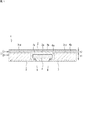
図1は、本発明の第1実施形態に係る高周波回路基板を示す断面模式図である。高周波回路基板1は、例えば自動車に搭載されるミリ波レーダ等のレーダセンサ装置で用いられるものである。本実施形態の高周波回路基板1は、グランド導体2、アンテナパターン(高周波回路パターン)3、電子部品4、及び誘電体層5を備えている。なお、以下の説明では、図1の上側を高周波回路基板1の「上側」とし、図2の下側を高周波回路基板1の「下側」とする(図2〜図11も同様)。
Next, a preferred embodiment of the present invention will be described with reference to the accompanying drawings.
[First Embodiment]
<Structure of high frequency circuit board>
FIG. 1 is a schematic cross-sectional view showing a high-frequency circuit board according to the first embodiment of the present invention. The high-frequency circuit board 1 is used in a radar sensor device such as a millimeter-wave radar mounted on an automobile, for example. The high-frequency circuit board 1 of the present embodiment includes a
グランド導体2は、例えば銅箔等の金属箔からなり、高周波回路基板1の最上層に配置されている。高周波回路パターンであるアンテナパターン3は、例えば銅箔等の金属箔にエッチング加工を施すことによって所望の形状に形成されている。本実施形態では、複数(図例では2個)のアンテナパターン3が、グランド導体2の下面(一面)から離反して高周波回路基板1の最下層に配置されている。なお、アンテナパターン3は1個だけでもよい。また、高周波回路パターンは、アンテナパターンに限定されるものではない。
The
電子部品4は、例えば、IC(パッケージされていないICも含む)、トランジスタ、ダイオード、抵抗、コンデンサ等からなる。本実施形態の電子部品4は、例えばMMIC(モノリシックマイクロ波集積回路)からなる。電子部品4は、各アンテナパターン3を跨ぐように配置された状態で、はんだ8によって各アンテナパターン3にはんだ付けされて実装されている。なお、電子部品4は、はんだ付け以外の方法でアンテナパターン3に実装されていてもよい。
The
誘電体層5は、主としてグランド導体2とアンテナパターン3との間に介在しており、熱可塑性樹脂13(図2B参照)を熱プレスして成形される第1誘電体層部6と、熱硬化性樹脂14(図4B参照)を熱プレスして成形される第2誘電体層部7とを有している。
The dielectric layer 5 is mainly interposed between the
熱可塑性樹脂13としては、ポリテトラフルオロエチレン(PTFE)樹脂,テトラフルオロエチレン・パーフルオロアルキルビニルエーテル共重合体(PFA)樹脂,ポリクロロトリフルオロエチレン(PCTFE)樹脂,テトラフルオロエチレン・ヘキサフルオロプロピレン共重合体(FEP)樹脂,ポリビニリデンフルオライド(PVdF)樹脂,
ポリフッ化ビニル(PVF)樹脂,テトラフルオロエチレン・エチレン共重合体(ETFE)樹脂,クロロトリフルオエチレン・エチレン共重合体(ECTFE)樹脂等のフッ素樹脂、ポリフェニレンエーテル(PPE)樹脂、変性ポリフェニレンエーテル(変形PPE)樹脂、液晶ポリマー(LCP)、及びこれらのポリマーアロイ等が挙げられる。熱硬化性樹脂14としては、エポキシ樹脂等が挙げられる。本実施形態では、熱可塑性樹脂13としてポリテトラフルオロエチレン樹脂が用いられ、熱硬化性樹脂14としてエポキシ樹脂が用いられている。
Examples of the
Fluororesin such as polyvinyl fluoride (PVF) resin, tetrafluoroethylene / ethylene copolymer (ETFE) resin, chlorotrifluoethylene / ethylene copolymer (ECTFE) resin, polyphenylene ether (PPE) resin, modified polyphenylene ether (modified) Examples thereof include PPE) resins, liquid crystal polymers (LCP), and polymer alloys thereof. Examples of the
第1誘電体層部6の下面の大部分は、各アンテナパターン3の上面に密着して固定されている。第1誘電体層部6は、各アンテナパターン3の外側(図1の左右両側)にも成形されており、その成形部分の下面は、各アンテナパターン3の下面と面一とされている。
Most of the lower surface of the first
第1誘電体層部6は、底部に各アンテナパターン3の一部が露出するキャビティ6aを有している。キャビティ6aは、その内部に電子部品4を収容した状態で各アンテナパターン3に電子部品4を実装可能な必要最小限の大きさに形成されている。第1誘電体層部6は、キャビティ6aに電子部品4が収容されることで、電子部品4と非接触とされている。
The first
第2誘電体層部7は、キャビティ6a内に成形されて電子部品を埋設している埋設部7aと、埋設部7aの上側に連続して成形されてグランド導体2の下面2a全体に密着して固定されている密着部7bとを有している。
The second dielectric layer portion 7 is formed in the
埋設部7aの外側面は、キャビティ6aの内側面に密着して固定されている。また、埋設部7aの下面の外側部分は、各アンテナパターン3の上面に密着して固定されている。埋設部7aの下面の内側部分は、両アンテナパターン3の間に成形されており、その成形部分の下面は、各アンテナパターン3の下面と面一とされている。
The outer surface of the buried
密着部7bの埋設部7aよりも外側に延びる外側部7b1の下面は、第1誘電体層部6におけるキャビティ6aを除く部分の上面6bに密着して固定されている。これにより、第2誘電体層部7の一部(外側部7b1)は、第1誘電体層部6の上面6bとグランド導体2の下面2aとの間に介在し、グランド導体2を第1誘電体層部6側に固定している。外側部7b1の積層方向(図1の上下方向)の厚みt2は、グランド導体2とアンテナパターン3との間における第1誘電体層部6の積層方向の厚みt1よりも薄く形成されている。
The lower surface of the outer portion 7b1 extending outward from the buried
<高周波回路基板の製造方法>
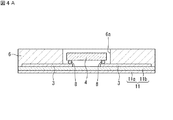
図2〜図5は、第1実施形態の高周波回路基板1の製造方法を示す断面模式図である。以下、図2〜図5を参照しながら、高周波回路基板1の製造方法について説明する。
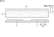
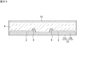
図2Aにおいて、まず、仮基材11の上面(一面)に積層した金属箔にエッチング加工を施して各アンテナパターン3を形成する(第1工程)。仮基材11は、例えば、ベースとなる銅箔11aの上面にニッケル箔11bを積層して構成されている。なお、仮基材11は、本実施形態の構成に限定されるものではない。
<Manufacturing method of high frequency circuit board>
2 to 5 are schematic cross-sectional views showing a method of manufacturing the high frequency circuit board 1 of the first embodiment. Hereinafter, a method for manufacturing the high frequency circuit board 1 will be described with reference to FIGS. 2 to 5.
In FIG. 2A, first, each
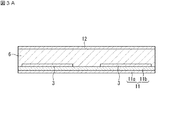
次に、図2Bに示すように、仮基材11の上面に熱可塑性樹脂13及び仮導体12をこの順に重ねた状態で、350℃以上の高温で熱プレスする。これにより、図3Aに示すように、仮基材11と仮導体12との間には、熱可塑性樹脂13から、各アンテナパターン3を覆う第1誘電体層部6が成形される(第2工程)。
Next, as shown in FIG. 2B, the
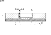
次に、図3Aに示す状態から仮導体12を除去した後、図3Bに示すように、第1誘電体層6に削り出し加工を施して、電子部品4を収容可能なキャビティ6aを形成する(第3工程)。これにより、キャビティ6aの底部には、各アンテナパターン3の一部が露出した状態となる。
Next, after removing the
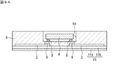
次に、図4Aに示すように、第1誘電体層部6のキャビティ6a内に電子部品4を挿入した状態で、電子部品4をはんだ8によって各アンテナパターン3にはんだ付けする。これにより、電子部品4は、第1誘電体層部6に非接触の状態で、各アンテナパターン3に実装される(第4工程)。
Next, as shown in FIG. 4A, the
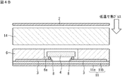
次に、図4Bに示すように、第1誘電体層部6におけるキャビティ6aの開口側に、熱硬化性樹脂14及びグランド導体2をこの順に重ねた状態で、220℃の低温で熱プレスする(第5工程)。その際、第1誘電体層部6の上面6bとグランド導体2の下面2aとの間に熱硬化性樹脂14の一部が残るように熱プレスする。
Next, as shown in FIG. 4B, the
これにより、図5に示すように、熱硬化性樹脂14から、キャビティ6a内の電子部品4を埋設した埋設部7a、及び第1誘電体層部6の上面6bとグランド導体2の下面2aとの間に介在する密着部7bを有する第2誘電体層部7が成形される。なお、第5工程では、1個の熱硬化性樹脂14を用いているが、埋設部7a用と密着部7b用の2個の熱硬化樹脂を用いてもよい。
As a result, as shown in FIG. 5, from the
次に、図5に示す状態から、仮基材11を除去する(第6工程)。これにより、図1に示す高周波回路基板1を得ることができる。
Next, the
<作用効果>
以上、第1実施形態における高周波回路基板1の製造方法によれば、アンテナパターン3を形成した仮基材11に熱可塑性樹脂13を熱プレスして第1誘電体層部6を成形した後に、第1誘電体層部6に形成したキャビティ6a内において電子部品4をアンテナパターン3に実装する。すなわち、電子部品4をアンテナパターン3に実装する前に熱可塑性樹脂13を熱プレスするため、熱可塑性樹脂13を高温で熱プレスすることに起因して電子部品4が熱破損するのを抑制することができる。
<Action effect>
As described above, according to the method for manufacturing the high-frequency circuit board 1 in the first embodiment, after the
また、電子部品4をアンテナパターン3に実装した後、第1誘電体層部6におけるキャビティ6aの開口側から熱硬化性樹脂14及びグランド導体2を熱プレスし、熱硬化性樹脂14から、キャビティ6a内の電子部品4を埋設した第2誘電体層部7を成形する。これにより、グランド導体2とアンテナパターン3との間には、電子部品4を埋設した第2誘電体層部7と、高周波特性の良い熱可塑性樹脂13からなる第1誘電体層部6とが介在するため、高周波回路基板1を小型化することができ、かつ高周波特性も向上させることができる。
Further, after mounting the
また、熱硬化性樹脂14及びグランド導体2を熱プレスする際に、第1誘電体層部6の上面6bとグランド導体2の下面2aとの間に、第2誘電体層部7の一部(外側部7b1)が成形されるように熱プレスするので、熱硬化性樹脂14からなる第2誘電体層部7の一部により、グランド導体2を第1誘電体層部6側に容易に固定することができる。
Further, when the
また、第2誘電体層部7の外側部7b1の厚みt2は、グランド導体2とアンテナパターン3との間における第1誘電体層部6の厚みt1よりも薄いので、熱硬化性樹脂14(第2誘電体層部7の外側部7b1)による高周波特性への悪影響を低減することができる。
Further, since the thickness t2 of the outer portion 7b1 of the second dielectric layer portion 7 is thinner than the thickness t1 of the first
また、熱可塑性樹脂13としてポリテトラフルオロエチレン(PTFE)樹脂を用いているため、フッ素樹脂であるテトラフルオロエチレン・パーフルオロアルキルビニルエーテル共重合体(PFA)樹脂よりも安価で容易に高周波回路基板を製造することができ、液晶ポリマー(LCP)樹脂よりも容易に高周波特性の良い高周波回路基板を製造することができる。
Further, since polytetrafluoroethylene (PTFE) resin is used as the
[第2実施形態]
図6は、本発明の第2実施形態に係る高周波回路基板を示す断面模式図である。本実施形態の高周波回路基板1では、各アンテナパターン3上の一部に、電子部品4を接続するためのパッド9がそれぞれ設けられている。本実施形態の各パッド9は、アンテナパターン3上のキャビティ6aに対応する位置に設けられている。
[Second Embodiment]
FIG. 6 is a schematic cross-sectional view showing a high frequency circuit board according to a second embodiment of the present invention. In the high-frequency circuit board 1 of the present embodiment,
本実施形態のキャビティ6aは、その底部に各パッド9の上面だけが露出するように形成されている。このため、本実施形態では、各アンテナパターン3の全体が、第1誘電体層部6により覆われている。各パッド9の上面には、はんだ8によって電子部品4がはんだ付けされて接続されている。これにより、電子部品4は、パッド9を介して各アンテナパターン3に実装されている。
The
第1誘電体層部6におけるキャビティ6aの下側部分は、両アンテナパターン3の間に成形されており、その成形部分の下面は、各アンテナパターン3の下面と面一とされている。第2誘電体層部7の埋設部7aの下面は、キャビティ6aの底面、及びパッド9の上面に密着して固定されている。
本実施形態の他の構成は、第1実施形態と同様であるため、同一の符号を付し、その説明を省略する。
The lower portion of the
Since the other configurations of the present embodiment are the same as those of the first embodiment, the same reference numerals are given and the description thereof will be omitted.
図7〜図10は、第2実施形態の高周波回路基板1の製造方法を示す断面模式図である。以下、図7〜図10を参照しながら、高周波回路基板1の製造方法について説明する。尚、以下の説明では、各アンテナパターン3上におけるパッド9が設けられる部分を「一部」といい、各アンテナパターン3上におけるパッド9が設けられない部分を「他部」という。
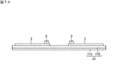
7 to 10 are schematic cross-sectional views showing a method of manufacturing the high frequency circuit board 1 of the second embodiment. Hereinafter, a method for manufacturing the high frequency circuit board 1 will be described with reference to FIGS. 7 to 10. In the following description, the portion on each
図7Aにおいて、まず、仮基材11の上面に積層した金属箔にエッチング加工を施して各アンテナパターン3を形成する。その後、各アンテナパターン3上の一部にパッド9を設ける(第1工程)。
In FIG. 7A, first, the metal foil laminated on the upper surface of the
次に、図7Bに示すように、仮基材11の上面に熱可塑性樹脂13及び仮導体12をこの順に重ねた状態で、350℃以上の高温で熱プレスする。これにより、図8Aに示すように、仮基材11と仮導体12との間には、熱可塑性樹脂13から、各アンテナパターン3上の他部及びパッド9を覆う第1誘電体層部6が成形される(第2工程)。
Next, as shown in FIG. 7B, the
次に、図8Aに示す状態から仮導体12を除去した後、図8Bに示すように、第1誘電体層6に削り出し加工を施して、電子部品4を収容可能なキャビティ6aを形成する(第3工程)。これにより、キャビティ6aの底部には、各アンテナパターン3上の他部が第1誘電体層部6に覆われたまま、各パッド9の上面が露出した状態となる。
Next, after removing the
次に、図9Aに示すように、第1誘電体層部6のキャビティ6a内に電子部品4を挿入した状態で、電子部品4をはんだ8によって各パッド9にはんだ付けする。これにより、電子部品4は、第1誘電体層部6に非接触の状態で、パッド9を介して各アンテナパターン3に実装される(第4工程)。
Next, as shown in FIG. 9A, the
次に、図9Bに示すように、第1誘電体層部6におけるキャビティ6aの開口側に熱硬化性樹脂14及びグランド導体2をこの順に重ねた状態で、220℃の低温で熱プレスする(第5工程)。その際、第1誘電体層部6の上面6bとグランド導体2の下面2aとの間に熱硬化性樹脂14の一部が残るように熱プレスする。
Next, as shown in FIG. 9B, the
これにより、図10に示すように、熱硬化性樹脂14から、キャビティ6a内の電子部品4を埋設した埋設部7a、及び第1誘電体層部6の上面6bとグランド導体2の下面2aとの間に介在する密着部7bを有する第2誘電体層部7が成形される。
次に、図10に示す状態から、仮基材11を除去する(第6工程)。これにより、図6に示す高周波回路基板1を得ることができる。
As a result, as shown in FIG. 10, from the
Next, the
以上、第2実施形態における高周波回路基板1の製造方法によっても、第1実施形態と同様の作用効果を奏する。また、第1誘電体層部6に削り出し加工を施しても、各アンテナパターン3上の他部は第1誘電体層部6に覆われたままなので、各アンテナパターン3上の第1誘電体層部6に覆われる面積を、第1実施形態よりも増やすことができる。これにより、高周波特性をさらに向上させることができる。
As described above, the method of manufacturing the high-frequency circuit board 1 in the second embodiment also has the same effect as that in the first embodiment. Further, even if the first
また、第1誘電体層部6におけるキャビティ6aの下側部分は、両アンテナパターン3の間にも成形されるため、第5工程(図9B参照)において、熱硬化性樹脂14を熱プレスしてキャビティ6a内に第2誘電体層部7を成形する際に、電子部品4の下方に潜り込ませる熱硬化性樹脂14の量を、第1実施形態(図4B参照)よりも減らすことができる。これにより、電子部品4の下方に第2誘電体層部7が成形されない隙間が生じるのを抑制することができる。
Further, since the lower portion of the
[第3実施形態]
図11は、本発明の第3実施形態に係る高周波回路基板を示す断面模式図である。本実施形態の高周波回路基板1は、第1実施形態の変形例であり、グランド導体2の上面(他面)に積層された複数(図例では3層)のガラスエポキシ樹脂層10を備えている。各ガラスエポキシ樹脂層10は、例えば、FR−4からなる基材10a上に、銅箔等の金属箔10bを貼り付けて構成されている。
[Third Embodiment]
FIG. 11 is a schematic cross-sectional view showing a high frequency circuit board according to a third embodiment of the present invention. The high-frequency circuit board 1 of the present embodiment is a modification of the first embodiment, and includes a plurality of (three layers in the example) glass epoxy resin layers 10 laminated on the upper surface (other surface) of the
本実施形態の他の構成は、第1実施形態と同様であるため、同一の符号を付し、その説明を省略する。
なお、ガラスエポキシ樹脂層10は、1層だけ積層されていてもよい。また、ガラスエポキシ樹脂層10は、第2実施形態のグランド導体2の上面に積層されていてもよい。
Since the other configurations of the present embodiment are the same as those of the first embodiment, the same reference numerals are given and the description thereof will be omitted.
In addition, only one glass
本実施形態の高周波回路基板1を製造する際には、第1実施形態と同様に第1〜第6工程(図2〜図5参照)を行った後、グランド導体2の上面に、基材10a及び金属箔10bをこの順に重ねた状態で熱プレスする。その際、熱プレスの温度は、約200℃であり、第1誘電体層部6(熱可塑性樹脂13)の溶融温度(350℃以上)よりも低いので、前記熱プレスにより第1誘電体層部6が溶融することはない。
When manufacturing the high-frequency circuit board 1 of the present embodiment, after performing the first to sixth steps (see FIGS. 2 to 5) in the same manner as in the first embodiment, a base material is placed on the upper surface of the
前記熱プレスの工程を繰り返し行うことで、グランド導体2の上面に、複数のガラスエポキシ樹脂層10が積層された高周波回路基板1を得ることができる。
By repeating the heat pressing process, a high frequency circuit board 1 in which a plurality of glass epoxy resin layers 10 are laminated on the upper surface of the
以上より、第3実施形態における高周波回路基板1の製造方法によっても、第1実施形態と同様の作用効果を奏する。また、高周波回路基板1がガラスエポキシ樹脂層10を備えることで、レーダセンサ装置に必要な回路(ベースバンド部回路や電源など)を配置することができるため、小型化することができる。
From the above, the method of manufacturing the high-frequency circuit board 1 in the third embodiment also has the same effect as that in the first embodiment. Further, since the high-frequency circuit board 1 includes the glass
[その他]
本発明の高周波回路基板は、レーダセンサ装置以外で用いられるものであってもよい。
[Other]
The high-frequency circuit board of the present invention may be used in a device other than the radar sensor device.
今回開示された実施形態はすべての点で例示であって制限的なものではないと考えられるべきである。本発明の範囲は、上記した意味ではなく、特許請求の範囲によって示され、特許請求の範囲と均等の意味、及び範囲内でのすべての変更が含まれることが意図される。 It should be considered that the embodiments disclosed this time are exemplary in all respects and not restrictive. The scope of the present invention is indicated by the scope of claims, not the above-mentioned meaning, and is intended to include the meaning equivalent to the scope of claims and all modifications within the scope.
1 高周波回路基板
2 グランド導体
3 アンテナパターン(高周波回路パターン)
4 電子部品
5 誘電体層
6 第1誘電体層部
6a キャビティ
7 第2誘電体層部
9 パッド
10 ガラスエポキシ樹脂層
11 仮基材
12 仮導体
13 熱可塑性樹脂
14 熱硬化性樹脂
t1 第1誘電体層部の厚み
t2 第2誘電体層部の一部の厚み
1 High
4 Electronic parts 5
Claims (9)
前記仮基材の前記一面に熱可塑性樹脂及び仮導体をこの順に重ねた状態で熱プレスし、前記熱可塑性樹脂から、前記高周波回路パターンを覆う第1誘電体層部を成形する第2工程と、
前記仮導体を除去した後に前記第1誘電体層に削り出し加工を施して、電子部品を収容可能なキャビティを形成する第3工程と、
前記キャビティ内において前記電子部品を前記高周波回路パターンに実装する第4工程と、
前記第1誘電体層部における前記キャビティの開口側に熱硬化性樹脂及びグランド導体をこの順に重ねた状態で熱プレスし、前記熱硬化性樹脂から、前記キャビティ内の前記電子部品を埋設した第2誘電体層部を成形する第5工程と、
前記仮基材を除去する第6工程と、をこの順に含む高周波回路基板の製造方法。 The first step of forming a high-frequency circuit pattern on one surface of the temporary base material,
A second step of forming a first dielectric layer portion covering the high frequency circuit pattern from the thermoplastic resin by heat pressing the thermoplastic resin and the temporary conductor in this order on the one surface of the temporary base material. ,
After removing the temporary conductor, the first dielectric layer is machined to form a cavity capable of accommodating electronic components.
A fourth step of mounting the electronic component in the high frequency circuit pattern in the cavity,
A thermosetting resin and a ground conductor were heat-pressed in this order on the opening side of the cavity in the first dielectric layer portion, and the electronic component in the cavity was embedded in the thermosetting resin. 2 The fifth step of forming the dielectric layer portion and
A method for manufacturing a high-frequency circuit board, comprising the sixth step of removing the temporary base material in this order.
前記第2工程では、熱プレスにより前記高周波回路パターン上の他部及び前記パッドを覆う前記第1誘電体層部を成形し、
前記第3工程では、前記キャビティの底部において、前記高周波回路パターン上の前記他部が前記第1誘電体層部に覆われたまま前記パッドが露出するまで、前記削り出し加工を施す、請求項1又は2に記載の高周波回路基板の製造方法。 In the first step, a pad for connecting the electronic component is further provided on a part of the high frequency circuit pattern.
In the second step, the other portion on the high frequency circuit pattern and the first dielectric layer portion covering the pad are formed by heat pressing.
In the third step, the machining process is performed at the bottom of the cavity until the pad is exposed while the other portion on the high frequency circuit pattern is covered with the first dielectric layer portion. The method for manufacturing a high frequency circuit board according to 1 or 2.
前記グランド導体の一面から離反して配置された高周波回路パターンと、
前記高周波回路パターンに実装された電子部品と、
前記グランド導体と前記高周波回路パターンとの間に介在する誘電体層と、を備え、
前記誘電体層は、
前記電子部品を収容したキャビティを有し、前記電子部品と非接触の第1誘電体層部と、
少なくとも前記キャビティ内に成形され、前記電子部品を埋設した第2誘電体層部と、を有し、
前記第1誘電体層部が熱可塑性樹脂からなり、前記第2誘電体層部が熱硬化性樹脂からなる、高周波回路基板。 With the ground conductor
A high-frequency circuit pattern arranged away from one surface of the ground conductor,
Electronic components mounted on the high-frequency circuit pattern and
A dielectric layer interposed between the ground conductor and the high frequency circuit pattern is provided.
The dielectric layer is
A first dielectric layer portion having a cavity accommodating the electronic component and not in contact with the electronic component,
It has at least a second dielectric layer portion formed in the cavity and embedded with the electronic component.
A high-frequency circuit board in which the first dielectric layer portion is made of a thermoplastic resin and the second dielectric layer portion is made of a thermosetting resin.
Priority Applications (3)
| Application Number | Priority Date | Filing Date | Title |
|---|---|---|---|
| JP2019022801A JP7231428B2 (en) | 2019-02-12 | 2019-02-12 | High-frequency circuit board manufacturing method, and high-frequency circuit board |
| DE102019117079.6A DE102019117079A1 (en) | 2019-02-12 | 2019-06-25 | METHOD OF MANUFACTURING A HIGH FREQUENCY CIRCUIT CIRCUIT BOARD AND HIGH FREQUENCY CIRCUIT CIRCUIT BOARD |
| US16/459,968 US10827604B2 (en) | 2019-02-12 | 2019-07-02 | Method for producing high frequency circuit board, and high frequency circuit board |
Applications Claiming Priority (1)
| Application Number | Priority Date | Filing Date | Title |
|---|---|---|---|
| JP2019022801A JP7231428B2 (en) | 2019-02-12 | 2019-02-12 | High-frequency circuit board manufacturing method, and high-frequency circuit board |
Publications (2)
| Publication Number | Publication Date |
|---|---|
| JP2020136282A true JP2020136282A (en) | 2020-08-31 |
| JP7231428B2 JP7231428B2 (en) | 2023-03-01 |
Family
ID=71738997
Family Applications (1)
| Application Number | Title | Priority Date | Filing Date |
|---|---|---|---|
| JP2019022801A Active JP7231428B2 (en) | 2019-02-12 | 2019-02-12 | High-frequency circuit board manufacturing method, and high-frequency circuit board |
Country Status (3)
| Country | Link |
|---|---|
| US (1) | US10827604B2 (en) |
| JP (1) | JP7231428B2 (en) |
| DE (1) | DE102019117079A1 (en) |
Families Citing this family (4)
| Publication number | Priority date | Publication date | Assignee | Title |
|---|---|---|---|---|
| US11375619B2 (en) * | 2019-09-24 | 2022-06-28 | Hongqisheng Precision Electronics (Qinhuangdao) Co., Ltd. | Method for manufacturing a packaging structure |
| KR20220014685A (en) * | 2020-07-29 | 2022-02-07 | 삼성전기주식회사 | Electronic component package and manufacturing method thereof |
| CN113993304A (en) * | 2021-09-26 | 2022-01-28 | 东莞康源电子有限公司 | Manufacturing method of high-density arbitrary interconnection type packaging carrier plate with buried copper block design |
| CN114340215A (en) * | 2021-12-15 | 2022-04-12 | 昆山沪利微电有限公司 | A 4D vehicle radar PCB board with small signal loss and its manufacturing method |
Citations (3)
| Publication number | Priority date | Publication date | Assignee | Title |
|---|---|---|---|---|
| JP2005223223A (en) * | 2004-02-06 | 2005-08-18 | Tdk Corp | Semiconductor IC-embedded substrate, manufacturing method thereof, and semiconductor IC-embedded module |
| JP2012079994A (en) * | 2010-10-05 | 2012-04-19 | Yamaichi Electronics Co Ltd | Component built-in printed circuit board and its manufacturing method |
| US20150016078A1 (en) * | 2013-07-15 | 2015-01-15 | Hong Kong Applied Science and Technology Research Institute Company Limited | Partitioned Hybrid Substrate for Radio Frequency Applications |
Family Cites Families (11)
| Publication number | Priority date | Publication date | Assignee | Title |
|---|---|---|---|---|
| US6852049B2 (en) * | 2003-01-24 | 2005-02-08 | Borgwarner Inc. | Ratcheting hydraulic chain tensioner with rotational reset and locking means |
| JP3709882B2 (en) * | 2003-07-22 | 2005-10-26 | 松下電器産業株式会社 | Circuit module and manufacturing method thereof |
| EP2136610A4 (en) * | 2008-01-25 | 2011-07-13 | Ibiden Co Ltd | MULTILAYER WIRING BOARD AND METHOD OF MANUFACTURING THE SAME |
| KR100965339B1 (en) * | 2008-06-04 | 2010-06-22 | 삼성전기주식회사 | Electronic component embedded printed circuit board and manufacturing method |
| KR20090130727A (en) * | 2008-06-16 | 2009-12-24 | 삼성전기주식회사 | Electronic component embedded printed circuit board and manufacturing method |
| US20140049928A1 (en) * | 2012-08-17 | 2014-02-20 | Taiyo Yuden Co., Ltd. | Substrate with built-in electronic component |
| US9666553B2 (en) * | 2014-06-16 | 2017-05-30 | Texas Instruments Incorporated | Millimeter wave integrated circuit with ball grid array package including transmit and receive channels |
| US10199337B2 (en) * | 2015-05-11 | 2019-02-05 | Samsung Electro-Mechanics Co., Ltd. | Electronic component package and method of manufacturing the same |
| US10115683B2 (en) * | 2016-04-14 | 2018-10-30 | Nxp Usa, Inc. | Electrostatic discharge protection for antenna using vias |
| JP6712765B2 (en) | 2016-05-31 | 2020-06-24 | パナソニックIpマネジメント株式会社 | High frequency board |
| EP3293814B1 (en) * | 2016-09-13 | 2020-04-29 | Dyconex AG | Circuit substrate and electronic super high frequency component |
-
2019
- 2019-02-12 JP JP2019022801A patent/JP7231428B2/en active Active
- 2019-06-25 DE DE102019117079.6A patent/DE102019117079A1/en active Pending
- 2019-07-02 US US16/459,968 patent/US10827604B2/en active Active
Patent Citations (3)
| Publication number | Priority date | Publication date | Assignee | Title |
|---|---|---|---|---|
| JP2005223223A (en) * | 2004-02-06 | 2005-08-18 | Tdk Corp | Semiconductor IC-embedded substrate, manufacturing method thereof, and semiconductor IC-embedded module |
| JP2012079994A (en) * | 2010-10-05 | 2012-04-19 | Yamaichi Electronics Co Ltd | Component built-in printed circuit board and its manufacturing method |
| US20150016078A1 (en) * | 2013-07-15 | 2015-01-15 | Hong Kong Applied Science and Technology Research Institute Company Limited | Partitioned Hybrid Substrate for Radio Frequency Applications |
Also Published As
| Publication number | Publication date |
|---|---|
| JP7231428B2 (en) | 2023-03-01 |
| US10827604B2 (en) | 2020-11-03 |
| US20200260572A1 (en) | 2020-08-13 |
| DE102019117079A1 (en) | 2020-08-13 |
Similar Documents
| Publication | Publication Date | Title |
|---|---|---|
| US10219390B2 (en) | Fabrication method of packaging substrate having embedded passive component | |
| US8233289B2 (en) | Multilayer wiring substrate and method for manufacturing the same | |
| JP7231428B2 (en) | High-frequency circuit board manufacturing method, and high-frequency circuit board | |
| US7888174B2 (en) | Embedded chip package process | |
| KR100610462B1 (en) | Solid electrolytic capacitor, transmission-line device, method of producing the same, and composite electronic component using the same | |
| WO2003103355A1 (en) | Composite multi-layer substrate and module using the substrate | |
| US9699892B2 (en) | Electric element-embedded multilayer substrate and method for manufacturing the same | |
| US20150055309A1 (en) | Electronic component embedded substrate and method of manufacturing electronic component embedded substrate | |
| KR20150026258A (en) | Rigid Flexible PCB and manufacture Method of It | |
| JP5093104B2 (en) | Interposer with built-in passive components | |
| US10051734B2 (en) | Wiring board and method for manufacturing the same | |
| JP2006324568A (en) | Multilayer module and manufacturing method thereof | |
| TWI864015B (en) | Method for manufacturing circuit board | |
| JP4065125B2 (en) | Component built-in module and manufacturing method thereof | |
| US10366822B2 (en) | Method of manufacturing winged coil structure | |
| US12028976B2 (en) | Board-to-board connection structure and method for manufacturing the same | |
| JP6268776B2 (en) | Multilayer substrate manufacturing method | |
| JP5516801B2 (en) | Component built-in board | |
| JP5481947B2 (en) | Manufacturing method of component-embedded substrate | |
| US20160021755A1 (en) | Chip embedded substrate and method of manufacturing the same | |
| JP2019096659A (en) | Electronic component and manufacturing method of electronic component | |
| JP5585035B2 (en) | Circuit board manufacturing method | |
| KR20110130604A (en) | Integrated printed circuit board containing a plurality of devices and a manufacturing method thereof | |
| KR20000059562A (en) | Flexible Substrates of Multi Metal Layer | |
| CN102668725B (en) | Wiring board and method of manufacturing wiring board |
Legal Events
| Date | Code | Title | Description |
|---|---|---|---|
| A621 | Written request for application examination |
Free format text: JAPANESE INTERMEDIATE CODE: A621 Effective date: 20210930 |
|
| A977 | Report on retrieval |
Free format text: JAPANESE INTERMEDIATE CODE: A971007 Effective date: 20220729 |
|
| A131 | Notification of reasons for refusal |
Free format text: JAPANESE INTERMEDIATE CODE: A131 Effective date: 20220823 |
|
| A521 | Request for written amendment filed |
Free format text: JAPANESE INTERMEDIATE CODE: A523 Effective date: 20221005 |
|
| TRDD | Decision of grant or rejection written | ||
| A01 | Written decision to grant a patent or to grant a registration (utility model) |
Free format text: JAPANESE INTERMEDIATE CODE: A01 Effective date: 20230207 |
|
| A61 | First payment of annual fees (during grant procedure) |
Free format text: JAPANESE INTERMEDIATE CODE: A61 Effective date: 20230216 |
|
| R150 | Certificate of patent or registration of utility model |
Ref document number: 7231428 Country of ref document: JP Free format text: JAPANESE INTERMEDIATE CODE: R150 |
|
| S533 | Written request for registration of change of name |
Free format text: JAPANESE INTERMEDIATE CODE: R313533 |
|
| R350 | Written notification of registration of transfer |
Free format text: JAPANESE INTERMEDIATE CODE: R350 |