JP2020122930A - Measurement device, exposure device and manufacturing method of article - Google Patents
Measurement device, exposure device and manufacturing method of article Download PDFInfo
- Publication number
- JP2020122930A JP2020122930A JP2019015987A JP2019015987A JP2020122930A JP 2020122930 A JP2020122930 A JP 2020122930A JP 2019015987 A JP2019015987 A JP 2019015987A JP 2019015987 A JP2019015987 A JP 2019015987A JP 2020122930 A JP2020122930 A JP 2020122930A
- Authority
- JP
- Japan
- Prior art keywords
- light
- polarizer
- polarized light
- substrate
- illumination
- Prior art date
- Legal status (The legal status is an assumption and is not a legal conclusion. Google has not performed a legal analysis and makes no representation as to the accuracy of the status listed.)
- Pending
Links
Images


Classifications
-
- G—PHYSICS
- G03—PHOTOGRAPHY; CINEMATOGRAPHY; ANALOGOUS TECHNIQUES USING WAVES OTHER THAN OPTICAL WAVES; ELECTROGRAPHY; HOLOGRAPHY
- G03F—PHOTOMECHANICAL PRODUCTION OF TEXTURED OR PATTERNED SURFACES, e.g. FOR PRINTING, FOR PROCESSING OF SEMICONDUCTOR DEVICES; MATERIALS THEREFOR; ORIGINALS THEREFOR; APPARATUS SPECIALLY ADAPTED THEREFOR
- G03F9/00—Registration or positioning of originals, masks, frames, photographic sheets or textured or patterned surfaces, e.g. automatically
- G03F9/70—Registration or positioning of originals, masks, frames, photographic sheets or textured or patterned surfaces, e.g. automatically for microlithography
- G03F9/7065—Production of alignment light, e.g. light source, control of coherence, polarization, pulse length, wavelength
-
- G—PHYSICS
- G03—PHOTOGRAPHY; CINEMATOGRAPHY; ANALOGOUS TECHNIQUES USING WAVES OTHER THAN OPTICAL WAVES; ELECTROGRAPHY; HOLOGRAPHY
- G03F—PHOTOMECHANICAL PRODUCTION OF TEXTURED OR PATTERNED SURFACES, e.g. FOR PRINTING, FOR PROCESSING OF SEMICONDUCTOR DEVICES; MATERIALS THEREFOR; ORIGINALS THEREFOR; APPARATUS SPECIALLY ADAPTED THEREFOR
- G03F9/00—Registration or positioning of originals, masks, frames, photographic sheets or textured or patterned surfaces, e.g. automatically
- G03F9/70—Registration or positioning of originals, masks, frames, photographic sheets or textured or patterned surfaces, e.g. automatically for microlithography
- G03F9/7049—Technique, e.g. interferometric
-
- G—PHYSICS
- G01—MEASURING; TESTING
- G01B—MEASURING LENGTH, THICKNESS OR SIMILAR LINEAR DIMENSIONS; MEASURING ANGLES; MEASURING AREAS; MEASURING IRREGULARITIES OF SURFACES OR CONTOURS
- G01B11/00—Measuring arrangements characterised by the use of optical techniques
-
- G—PHYSICS
- G03—PHOTOGRAPHY; CINEMATOGRAPHY; ANALOGOUS TECHNIQUES USING WAVES OTHER THAN OPTICAL WAVES; ELECTROGRAPHY; HOLOGRAPHY
- G03B—APPARATUS OR ARRANGEMENTS FOR TAKING PHOTOGRAPHS OR FOR PROJECTING OR VIEWING THEM; APPARATUS OR ARRANGEMENTS EMPLOYING ANALOGOUS TECHNIQUES USING WAVES OTHER THAN OPTICAL WAVES; ACCESSORIES THEREFOR
- G03B27/00—Photographic printing apparatus
- G03B27/72—Controlling or varying light intensity, spectral composition, or exposure time in photographic printing apparatus
- G03B27/74—Positioning exposure meters in the apparatus
-
- G—PHYSICS
- G03—PHOTOGRAPHY; CINEMATOGRAPHY; ANALOGOUS TECHNIQUES USING WAVES OTHER THAN OPTICAL WAVES; ELECTROGRAPHY; HOLOGRAPHY
- G03F—PHOTOMECHANICAL PRODUCTION OF TEXTURED OR PATTERNED SURFACES, e.g. FOR PRINTING, FOR PROCESSING OF SEMICONDUCTOR DEVICES; MATERIALS THEREFOR; ORIGINALS THEREFOR; APPARATUS SPECIALLY ADAPTED THEREFOR
- G03F9/00—Registration or positioning of originals, masks, frames, photographic sheets or textured or patterned surfaces, e.g. automatically
- G03F9/70—Registration or positioning of originals, masks, frames, photographic sheets or textured or patterned surfaces, e.g. automatically for microlithography
- G03F9/7003—Alignment type or strategy, e.g. leveling, global alignment
- G03F9/7046—Strategy, e.g. mark, sensor or wavelength selection
-
- G—PHYSICS
- G03—PHOTOGRAPHY; CINEMATOGRAPHY; ANALOGOUS TECHNIQUES USING WAVES OTHER THAN OPTICAL WAVES; ELECTROGRAPHY; HOLOGRAPHY
- G03F—PHOTOMECHANICAL PRODUCTION OF TEXTURED OR PATTERNED SURFACES, e.g. FOR PRINTING, FOR PROCESSING OF SEMICONDUCTOR DEVICES; MATERIALS THEREFOR; ORIGINALS THEREFOR; APPARATUS SPECIALLY ADAPTED THEREFOR
- G03F9/00—Registration or positioning of originals, masks, frames, photographic sheets or textured or patterned surfaces, e.g. automatically
- G03F9/70—Registration or positioning of originals, masks, frames, photographic sheets or textured or patterned surfaces, e.g. automatically for microlithography
- G03F9/7069—Alignment mark illumination, e.g. darkfield, dual focus
-
- G—PHYSICS
- G03—PHOTOGRAPHY; CINEMATOGRAPHY; ANALOGOUS TECHNIQUES USING WAVES OTHER THAN OPTICAL WAVES; ELECTROGRAPHY; HOLOGRAPHY
- G03F—PHOTOMECHANICAL PRODUCTION OF TEXTURED OR PATTERNED SURFACES, e.g. FOR PRINTING, FOR PROCESSING OF SEMICONDUCTOR DEVICES; MATERIALS THEREFOR; ORIGINALS THEREFOR; APPARATUS SPECIALLY ADAPTED THEREFOR
- G03F9/00—Registration or positioning of originals, masks, frames, photographic sheets or textured or patterned surfaces, e.g. automatically
- G03F9/70—Registration or positioning of originals, masks, frames, photographic sheets or textured or patterned surfaces, e.g. automatically for microlithography
- G03F9/7088—Alignment mark detection, e.g. TTR, TTL, off-axis detection, array detector, video detection
-
- G—PHYSICS
- G03—PHOTOGRAPHY; CINEMATOGRAPHY; ANALOGOUS TECHNIQUES USING WAVES OTHER THAN OPTICAL WAVES; ELECTROGRAPHY; HOLOGRAPHY
- G03F—PHOTOMECHANICAL PRODUCTION OF TEXTURED OR PATTERNED SURFACES, e.g. FOR PRINTING, FOR PROCESSING OF SEMICONDUCTOR DEVICES; MATERIALS THEREFOR; ORIGINALS THEREFOR; APPARATUS SPECIALLY ADAPTED THEREFOR
- G03F9/00—Registration or positioning of originals, masks, frames, photographic sheets or textured or patterned surfaces, e.g. automatically
- G03F9/70—Registration or positioning of originals, masks, frames, photographic sheets or textured or patterned surfaces, e.g. automatically for microlithography
- G03F9/7092—Signal processing
Abstract
Description
本発明は、計測装置、露光装置及び物品の製造方法に関する。 The present invention relates to a measuring device, an exposure device, and an article manufacturing method.
半導体デバイスの製造に用いられる露光装置においては、近年、微細化とともに、基板の重ね合わせ精度(オーバーレイ精度)の高精度化が求められている。オーバーレイ精度には、一般的に、解像度の1/5程度が必要とされるため、半導体デバイスの微細化が進むにつれて、益々、オーバーレイ精度の向上が重要となる。 In recent years, exposure apparatuses used for manufacturing semiconductor devices have been required to have higher precision in overlaying (overlay precision) of substrates as well as miniaturization. Since overlay accuracy generally requires about ⅕ of the resolution, it is increasingly important to improve overlay accuracy as semiconductor devices become finer.
オーバーレイ精度の向上のためには、位置計測系を高精度に調整することが必要となる。例えば、位置計測系の計測だまされを低減するために、位置計測系のコマ収差と光軸ずれとを分離して高精度に調整する技術が提案されている(特許文献1参照)。 In order to improve overlay accuracy, it is necessary to adjust the position measurement system with high accuracy. For example, there has been proposed a technique for separating the coma aberration and the optical axis shift of the position measurement system with high accuracy in order to reduce the measurement deception of the position measurement system (see Patent Document 1).
また、オーバーレイ精度の更なる向上のためには、アライメントマークを検出するための光(検出光)の波長の広帯域化が考えられる。特に、近年では、カラーフィルタ工程など、可視光ではコントラストが低く、精度が低いプロセスが増えており、可視光以外の青波長の光や近赤外光などを含む幅広い波長帯の光を使用可能な位置計測系が求められている。 Further, in order to further improve the overlay accuracy, it is conceivable to widen the wavelength band of the light (detection light) for detecting the alignment mark. In particular, in recent years, the number of processes that have low contrast and low accuracy in visible light, such as the color filter process, has increased, and it is possible to use light in a wide wavelength band including blue wavelength light and near infrared light other than visible light. An accurate position measurement system is required.
しかしながら、従来の位置計測系では、検出光の波長を広帯域化した際に、コントラストが低下し、その結果、計測精度やオーバーレイ精度の低下を招いてしまう。これは、照明光学系と結像光学系との合成に用いられる偏光ビームスプリッタなどのS偏光とP偏光とで反射率が異なる部分反射材の特性(膜特性)が完全ではないことに起因する。具体的には、波長帯域が狭ければ、高精度な偏光ビームスプリッタの特性を実現することができるが、波長帯域が広帯域化すると、高精度な偏光ビームスプリッタの特性を実現することができない。これにより、偏光ビームスプリッタでカットしきれなかった偏光成分がフレアとなり、かかるフレアによって位置計測系のコントラストが低下してしまう。 However, in the conventional position measurement system, the contrast is lowered when the wavelength of the detection light is broadened, and as a result, the measurement accuracy and the overlay accuracy are deteriorated. This is because the characteristics (film characteristics) of the partially reflective material, such as a polarization beam splitter used for combining the illumination optical system and the imaging optical system, having different reflectances between S-polarized light and P-polarized light are not perfect. .. Specifically, if the wavelength band is narrow, high-precision polarization beam splitter characteristics can be realized, but if the wavelength band is wide, high-precision polarization beam splitter characteristics cannot be realized. As a result, the polarization component that cannot be completely cut by the polarization beam splitter becomes flare, and the flare reduces the contrast of the position measurement system.
本発明は、このような従来技術の課題に鑑みてなされ、被検物体の位置を計測する計測精度の点で有利な計測装置を提供することを例示的目的とする。 The present invention has been made in view of the above problems of the conventional art, and an exemplary object of the present invention is to provide a measuring device advantageous in terms of measurement accuracy for measuring the position of an object to be inspected.
上記目的を達成するために、本発明の一側面としての計測装置は、被検物体の位置を計測する計測装置であって、前記被検物体を照明光で照明する照明系と、前記被検物体からの検出光を、前記被検物体の像を検出する光電変換素子に結像する結像系と、前記照明系と前記結像系との間に配置された反射型偏光子及びλ/4板とを含み、前記反射型偏光子及び前記λ/4板を介して前記照明光と前記検出光とを分離する分離系と、を有し、前記分離系は、前記反射型偏光子と前記λ/4板との間に配置された少なくとも1つの光学部材を含み、前記照明系及び前記結像系の少なくとも一方は、偏光子を含むことを特徴とする。 In order to achieve the above object, a measuring device according to one aspect of the present invention is a measuring device for measuring a position of an object to be inspected, the illumination system illuminating the object to be inspected with illumination light, and the inspected object. An imaging system that forms the detection light from the object on a photoelectric conversion element that detects an image of the object to be inspected, and a reflective polarizer and λ/ that are arranged between the illumination system and the imaging system. And a separation system that separates the illumination light and the detection light via the reflection type polarizer and the λ/4 plate, the separation system including the reflection type polarizer and the reflection type polarizer. At least one optical member is arranged between the λ/4 plate and at least one of the illumination system and the imaging system includes a polarizer.
本発明の更なる目的又はその他の側面は、以下、添付図面を参照して説明される実施形態によって明らかにされるであろう。 Further objects and other aspects of the present invention will be made clear by the embodiments described below with reference to the accompanying drawings.
本発明によれば、例えば、被検物体の位置を計測する計測精度の点で有利な計測装置を提供することができる。 According to the present invention, for example, it is possible to provide a measuring device which is advantageous in terms of measurement accuracy for measuring the position of the object to be inspected.
以下、添付図面を参照して実施形態を詳しく説明する。なお、以下の実施形態は特許請求の範囲に係る発明を限定するものでない。実施形態には複数の特徴が記載されているが、これらの複数の特徴の全てが発明に必須のものとは限らず、また、複数の特徴は任意に組み合わせられてもよい。更に、添付図面においては、同一もしくは同様の構成に同一の参照番号を付し、重複した説明は省略する。 Hereinafter, embodiments will be described in detail with reference to the accompanying drawings. The following embodiments do not limit the invention according to the claims. Although a plurality of features are described in the embodiment, not all of the plurality of features are essential to the invention, and the plurality of features may be arbitrarily combined. Furthermore, in the accompanying drawings, the same or similar components are designated by the same reference numerals, and a duplicate description will be omitted.
図1は、本発明の一側面としての露光装置100の構成を示す概略図である。露光装置100は、パターンを基板に形成するリソグラフィ装置である。露光装置100は、レチクル1を保持するレチクルステージ2と、基板3を保持する基板ステージ4と、レチクルステージ2に保持されたレチクル1を照明する照明光学系5とを有する。また、露光装置100は、レチクル1のパターン(の像)を基板ステージ4に保持された基板3に投影する投影光学系6と、露光装置100の全体の動作を統括的に制御する制御部17とを有する。
FIG. 1 is a schematic diagram showing a configuration of an
露光装置100は、本実施形態では、レチクル1と基板3とを走査方向に互いに同期走査しながら(即ち、ステップ・アンド・スキャン方式で)、レチクル1のパターンを基板3に転写する走査型露光装置(スキャナー)である。但し、露光装置100は、レチクル1を固定して(即ち、ステップ・アンド・リピート方式で)、レチクル1のパターンを基板3に転写する露光装置(ステッパー)であってもよい。
In the present embodiment, the
以下では、投影光学系6の光軸と一致する方向(光軸方向)をZ軸方向、Z軸方向に垂直な平面内でレチクル1及び基板3の走査方向をY軸方向、Z軸方向及びY軸方向に垂直な方向(非走査方向)をX軸方向とする。また、X軸周り、Y軸周り及びZ軸周りのそれぞれの方向を、θX方向、θY方向及びθZ方向とする。
In the following, the direction (optical axis direction) that coincides with the optical axis of the projection
照明光学系5は、レチクル1、具体的には、レチクル上の所定の照明領域を、均一な照度分布の光(露光光)で照明する。露光光としては、例えば、超高圧水銀ランプのg線やi線、KrFエキシマレーザ、ArFエキシマレーザ、F2レーザなどが用いられる。また、より微細な半導体デバイスを製造するために、数nm〜数百nmの極端紫外光(Extreme Ultra Violet:EUV光)を露光光として用いてもよい。
The illumination
レチクルステージ2は、レチクル1を保持し、投影光学系6の光軸に垂直な平面内、即ち、XY平面内で2次元移動可能に、且つ、θZ方向に回転可能に構成されている。レチクルステージ2は、リニアモータなどの駆動装置(不図示)によって駆動される。
The
レチクルステージ2には、ミラー7が設けられている。また、ミラー7に対応する位置には、レーザ干渉計9が設けられている。レチクルステージ2の2次元方向の位置及び回転角はレーザ干渉計9によってリアルタイムで計測され、かかる計測結果は制御部17に出力される。制御部17は、レーザ干渉計9の計測結果に基づいて駆動装置を制御し、レチクルステージ2に保持されたレチクル1を位置決めする。
A mirror 7 is provided on the
投影光学系6は、複数の光学素子を含み、レチクル1のパターンを所定の投影倍率βで基板3に投影する。投影光学系6は、本実施形態では、例えば、1/4又は1/5の投影倍率βを有する縮小光学系である。
The projection
基板ステージ4は、チャックを介して基板3を保持するZステージと、Zステージを支持するXYステージと、XYステージを支持するベースとを含む。基板ステージ4は、リニアモータなどの駆動装置(不図示)によって駆動される。
The substrate stage 4 includes a Z stage that holds the
基板ステージ4には、ミラー8が設けられている。また、ミラー8に対向する位置には、レーザ干渉計10及び12が設けられている。基板ステージ4のX軸方向、Y軸方向及びθZ方向の位置はレーザ干渉計10によってリアルタイムで計測され、かかる計測結果は制御部17に出力される。同様に、基板ステージ4のZ軸方向の位置、θX方向及びθY方向の位置はレーザ干渉計12によってリアルタイムで計測され、かかる計測結果は制御部17に出力される。制御部17は、レーザ干渉計10及び12の計測結果に基づいて駆動装置を制御し、基板ステージ4に保持された基板3を位置決めする。
A
レチクルアライメント計測系13は、レチクルステージ2の近傍に設けられている。レチクルアライメント計測系13は、レチクルステージ2に保持されたレチクル1に設けられたレチクル基準マーク(不図示)と、投影光学系6を介して基板ステージ4に配置されたステージ基準プレート11に設けられた基準マーク38とを検出する。レチクルアライメント計測系13は、基板3を実際に露光する際に用いられる光源と同一の光源を用いて、レチクル1に設けられたレチクル基準マークと、投影光学系6を介して基準マーク38とを検出する。具体的には、レチクルアライメント計測系13は、レチクル基準マーク及び基準マーク38からの反射光を撮像素子(例えば、CCDカメラなどの光電変換素子)で検出する。かかる撮像素子からの検出信号に基づいて、レチクル1と基板3との位置合わせ(アライメント)が行われる。この際、レチクル1に設けられたレチクル基準マークとステージ基準プレート11に設けられた基準マーク38との位置及びフォーカスを合わせることで、レチクル1と基板3との相対的な位置関係(X、Y、Z)を合わせることができる。
The reticle
レチクルアライメント計測系14は、基板ステージ4に配置されている。レチクルアライメント計測系14は、透過型の計測系であって、基準マーク38が透過型のマークである場合に用いられる。レチクルアライメント計測系14は、基板3を実際に露光する際に用いられる光源と同一の光源を用いて、レチクル1に設けられたレチクル基準マーク及び基準マーク38を検出する。具体的には、レチクルアライメント計測系14は、レチクル基準マーク及び基準マーク38を通過した透過光を光量センサで検出する。この際、基板ステージ4をX軸方向(又はY軸方向)及びZ軸方向に移動させながら、レチクルアライメント計測系14は、透過光の光量を検出する。これにより、レチクル1に設けられたレチクル基準マークとステージ基準プレート11に設けられた基準マーク38との位置及びフォーカスを合わせることができる。
The reticle
このように、レチクルアライメント計測系13、或いは、レチクルアライメント計測系14のどちらの計測系を用いても、レチクル1と基板3との相対的な位置関係(X、Y、Z)を合わせることができる。
As described above, the relative positional relationship (X, Y, Z) between the
ステージ基準プレート11は、基板ステージ4に保持された基板3の表面とほぼ同じ高さになるように、基板ステージ4のコーナーに配置されている。ステージ基準プレート11は、基板ステージ4の1つのコーナーに配置されていてもよいし、基板ステージ4の複数のコーナーに配置されていてもよい。
The
ステージ基準プレート11は、図2に示すように、レチクルアライメント計測系13又は14によって検出される基準マーク38と、基板アライメント計測系16によって検出される基準マーク39とを有する。ステージ基準プレート11は、複数の基準マーク38や複数の基準マーク39を有していてもよい。また、基準マーク38と基準マーク39との位置関係(X軸方向及びY軸方向)は、所定の位置関係に設定されている(即ち、既知である)。なお、基準マーク38と基準マーク39とは、共通のマークであってもよい。
As shown in FIG. 2, the
フォーカス計測系15は、基板3の表面に光を斜入射で投光する投光系と、基板3の表面で反射した光を受光する受光系とを含む。フォーカス計測系15は、基板3のZ軸方向の位置を計測し、かかる計測結果を制御部17に出力する。制御部17は、フォーカス計測系15の計測結果に基づいて基板ステージ4を駆動する駆動装置を制御し、基板ステージ4に保持された基板3のZ軸方向の位置及び傾斜角を調整する。
The
基板アライメント計測系16は、後述するように、照明系ILと、結像系IMとを含む。照明系ILは、基板3に設けられたアライメントマーク19やステージ基準プレート11に設けられた基準マーク39を光(照明光)で照明する。結像系IMは、基板3に設けられたアライメントマーク19やステージ基準プレート11に設けられた基準マーク39からの光(検出光)を、これらの像を検出する光電変換素子に結像する。基板アライメント計測系16は、アライメントマーク19や基準マーク39の位置を計測し、かかる計測結果を制御部17に出力する。制御部17は、基板アライメント計測系16の計測結果に基づいて基板ステージ4を駆動する駆動装置を制御し、基板ステージ4に保持された基板3のX軸方向及びY軸方向の位置を調整する。
The substrate
基板アライメント計測系の構成は、一般的には、オフアクシスアライメント(OA)計測系と、TTL(Through the Lens Alignment)計測系との2つに大別される。OA計測系は、投影光学系を介さずに、基板に設けられたアライメントマークを光学的に検出する。TTL計測系は、投影光学系を介して、露光光の波長とは異なる波長の光(非露光光)を用いて基板に設けられたアライメントマークを検出する。基板アライメント計測系16は、本実施形態では、OA計測系であるが、本発明は、アライメントの検出方式を限定するものではない。例えば、基板アライメント計測系16がTTL計測系である場合には、投影光学系6を介して、基板に設けられたアライメントマークを検出するが、基本的な構成は、OA計測系と同様である。
The configuration of the substrate alignment measurement system is generally roughly classified into an off-axis alignment (OA) measurement system and a TTL (Through the Lens Alignment) measurement system. The OA measurement system optically detects the alignment mark provided on the substrate without using the projection optical system. The TTL measurement system detects an alignment mark provided on the substrate using light having a wavelength different from the wavelength of the exposure light (non-exposure light) via the projection optical system. The substrate
制御部17は、例えば、CPUやメモリなどを含むコンピュータで構成され、記憶部に記憶されたプログラムに従って露光装置100の各部を統括的に制御する。制御部17は、レチクル1のパターンを基板3に転写する、即ち、基板3を露光する露光処理を制御する。露光処理において、制御部17は、例えば、基板アライメント計測系16の計測結果に基づいて、基板ステージ4の位置を制御する。
The
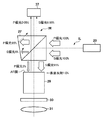
図3を参照して、基板アライメント計測系16について詳細に説明する。図3は、基板アライメント計測系16の具体的な構成を示す概略図である。基板アライメント計測系16は、被検物体である基板3に設けられたアライメントマーク19を検出して基板3の位置を計測する計測装置として機能する。
The substrate
基板アライメント計測系16は、光源20と、第1コンデンサ光学系21と、波長フィルタ板22と、第2コンデンサ光学系23と、開口絞り板24と、第1照明系25と、第2照明系26と、偏光ビームスプリッタ27と、NA絞り28とを含む。また、基板アライメント計測系16は、AFプリズム29と、λ/4板30と、対物レンズ31と、リレーレンズ32と、第1結像系33と、開口絞り34と、第2結像系35と、波長シフト差調整用光学部材36と、光電変換素子37とを含む。
The substrate
本実施形態では、第1コンデンサ光学系21、波長フィルタ板22、第2コンデンサ光学系23、開口絞り板24、第1照明系25及び第2照明系26は、照明系ILを構成する。リレーレンズ32、第1結像系33、開口絞り34、第2結像系35及び波長シフト差調整用光学部材36は、結像系IMを構成する。また、照明系ILと結像系IMとの間に配置された偏光ビームスプリッタ27、NA絞り28、AFプリズム29、λ/4板30及び対物レンズ31は、分離系DSを構成する。分離系DSは、照明系ILと結像系IMとを合成する光学系である。分離系DSは、本実施形態では、照明光と検出光とを分離する機能を有する。
In the present embodiment, the first condenser
光源20は、アライメントマーク19を照明するための光(照明光)として、300nm以上の波長帯域の幅を有する光を射出(出力)する。光源20は、本実施形態では、可視光(例えば、500nm以上700nm以下の波長の光)、青波長の光(例えば、450nm以上550nm以下の波長の光(青波長光))及び赤外光(例えば、700nm以上1500nm以下の波長の光)を射出する。光源20からの光(照明光)は、第1コンデンサ光学系21、波長フィルタ板22及び第2コンデンサ光学系23を通過して、基板アライメント計測系16の瞳面(物体面に対する光学的なフーリエ変換面)に位置する開口絞り板24に到達する。
The
波長フィルタ板22は、光源20と光電変換素子37との間の光路に配置されている。波長フィルタ板22には、光を通過させる波長帯が互いに異なる複数の波長フィルタが配置され、制御部17の制御下において、複数の波長フィルタから1つの波長フィルタが選択されて基板アライメント計測系16の光路に配置される。本実施形態では、波長フィルタ板22には、赤外光を通過させる波長フィルタと、可視光を通過させる波長フィルタと、青波長光を通過させる波長フィルタとが配置されている。波長フィルタ板22において、これらの波長フィルタを切り替えることによって、基板3に設けられたアライメントマーク19を照明する光の波長帯を選択することができる。また、波長フィルタ板22は、予め設けられた複数の波長フィルタの他に、新たな波長フィルタを追加することが可能な構成を有していてもよい。
The
開口絞り板24には、照明σが互いに異なる複数の開口絞りが配置され、制御部17の制御下において、基板アライメント計測系16の光路に配置する開口絞りを切り替えることで、アライメントマーク19を照明する光の照明σを変更することができる。また、開口絞り板24は、予め設けられた複数の開口絞りの他に、新たな開口絞りを追加することが可能な構成を有していてもよい。
A plurality of aperture stops having different illumination σ are arranged on the
開口絞り板24に到達した光は、第1照明系25及び第2照明系26を介して、偏光ビームスプリッタ27に導かれる。偏光ビームスプリッタ27に導かれた光のうち紙面に垂直なS偏光は、偏光ビームスプリッタ27で反射され、NA絞り28、AFプリズム29及びλ/4板30を通過して円偏光に変換される。λ/4板30を通過した光は、対物レンズ31を介して、基板3に設けられたアライメントマーク19を照明する。NA絞り28は、制御部17の制御下において、絞り量を変えることでNAを変更することができる。
The light that has reached the
アライメントマーク19からの反射光、回折光及び散乱光(検出光)は、対物レンズ31及びλ/4板30を通過して紙面に平行なP偏光に変換され、NA絞り28を介して、偏光ビームスプリッタ27を透過する。偏光ビームスプリッタ27を透過した光は、リレーレンズ32、第1結像系33、開口絞り34、第2結像系35及び波長シフト差調整用光学部材36を介して、光電変換素子(例えば、CCDイメージセンサなどの撮像素子)37に到達する。光電変換素子37に到達する光は、光電変換素子上にアライメントマーク19の像を形成し、かかる像を光電変換素子37が検出する。光電変換素子37は、アライメントマーク19からの光を検出するが、かかる光の強度がある一定の閾値を超えるまで、蓄積時間を延ばすことが可能である。光電変換素子37の蓄積時間は、制御部17によって制御される。また、制御部17は、光電変換素子37からの出力信号(光電変換素子上に形成されたアライメントマーク19の像に対応するアライメント信号)に基づいて、基板3の位置を求める。
The reflected light, diffracted light, and scattered light (detection light) from the
また、基板アライメント計測系16は、基板アライメント計測用のフォーカス計測系(AF計測系)40を含む。図4及び図5を参照して、AF計測系40を詳細に説明する。図4及び図5は、AF計測系40がフォーカス計測をしている状態を示している。具体的には、図4は、AF計測系40が基板3にフォーカス計測光(AF光)を照射している状態を示し、図5は、AF計測系40が基板3で反射されたAF光を受光している状態を示している。
The substrate
図4を参照するに、AF光源41から射出されたAF光は、レンズ42を介して、AF計測用パターン43をケーラー照明する。AF光源41は、基板アライメントに用いない波長帯の光をAF光として射出し、かかるAF光は、AFプリズム29で反射される。AFプリズム29は、本実施形態では、ダイクロイックプリズムで構成されている。AF計測用パターン43は、ガラス基板にスリットパターンを描画することで構成されている。AF計測用パターン43のスリットパターンを通過したAF光は、レンズ44を介してミラー45で反射され、レンズ46に到達する。この際、AF光は、レンズ46の中心ではなく、レンズ46の中心から偏心した部分に到達し、レンズ46で屈折することによって、基準ミラー47を通過し、レンズ48に到達する。レンズ48に到達するAF光も同様に、レンズ48の中心ではなく、レンズ48の中心から偏心した部分に到達する。なお、図4では、AF計測用パターン43よりも後段においては、AF光の主光線のみを示しているが、実際には、AF光はNAを有する光線である。
Referring to FIG. 4, the AF light emitted from the AF
レンズ48に到達したAF光は、レンズ48で屈折し、AFプリズム29に到達する。AFプリズム29は、AF光源41からのAF光を反射し、光源20からの光を透過する特性を有するプリズムで構成されている。AFプリズム29で反射されたAF光は、λ/4板30を透過し、対物レンズ31に到達する。この際、AF光は、対物レンズ31の中心ではなく、対物レンズ31の中心から偏心した部分に到達し、対物レンズ31で屈折することによって、図4に示すように、基板3に対して角度θを有して入射(斜入射)する。
The AF light reaching the
図5を参照するに、基板3に入射したAF光は、角度θで反射され、対物レンズ31に到達する。この際、AF光は、対物レンズ31の中心ではなく、対物レンズ31の中心から偏心した部分に到達し、対物レンズ31で屈折することによって、λ/4板30を透過し、AFプリズム29に到達する。なお、図5では、AF光の主光線のみを示しているが、実際には、AF光はNAを有する光線である。
With reference to FIG. 5, the AF light incident on the
AFプリズム29で反射したAF光は、レンズ48に到達する。この際、AF光は、レンズ48の中心ではなく、レンズ48の中心から偏心した部分に到達し、レンズ48で屈折することによって、基準ミラー47を通過し、レンズ46に到達する。この際、AF光は、レンズ46の中心ではなく、レンズ46の中心から偏心した部分に到達し、レンズ46で屈折することによって、レンズ49の中心に到達する。レンズ49に到達したAF光は、レンズ49を通過して、AFセンサ50で受光される。
The AF light reflected by the
本実施形態では、AF計測系40において、基板3に対してAF光を斜入射で照射し、基板3で反射したAF光をAFセンサ50で受光する場合を説明した。この場合、基板3がZ軸方向(フォーカス方向)に移動すると、それに応じて、AFセンサ50で受光するAF光がシフトする(ずれる)ことがわかる。このように、AF計測系40は、基板3を斜入射照明することによって、基板3のフォーカス計測をすることが可能となる。
In the present embodiment, the case where the AF light is obliquely incident on the
基板アライメント計測系16が基板3に設けられたアライメントマーク19を検出する場合、アライメントマーク19の上には、レジスト(透明層)が塗布(形成)されているため、単色光又は狭い波長帯の光では干渉縞が発生してしまう。従って、光電変換素子37からのアライメント信号に干渉縞の信号が加算され、アライメントマーク19を高精度に検出することができなくなる。そこで、一般的には、広帯域の波長の光を射出する光源を光源20として用いて、光電変換素子37からのアライメント信号に干渉縞の信号が加算されることを低減している。
When the substrate
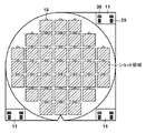
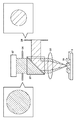
上述したように、基板アライメント計測系16では、レジストに起因する干渉縞を低減するために、広帯域の波長の光を用いているが、近年では、特定の波長の光しか通さないカラーフィルタを扱う工程(カラーフィルタ工程)が増えている。カラーフィルタは、図6に示すように、CCDイメージセンサやCMOSイメージセンサなどのセンサ上に配置される色選択用フィルタである。カラーフィルタを通すことで、センサの画素に色の情報をもたせることができる。具体的には、図6に示すように、カラーフィルタにブロードな波長の光51が入射すると、カラーフィルタを通過することができる光52のみがセンサに到達し、センサの画素に色の情報をもたせることができる。
As described above, the substrate
例えば、RGBカラーフィルタ工程では、図7に示すように、赤波長(R)の光、緑波長(G)の光及び青波長(B)の光のそれぞれを通すカラーフィルタがセンサ上に並列に配置される。RGBカラーフィルタ工程におけるデバイス製造では、各カラーフィルタを介してアライメントを行わなければならないため、青波長から赤波長まで幅広く波長帯を切り替える必要がある。 For example, in the RGB color filter process, as shown in FIG. 7, color filters that pass light of red wavelength (R), light of green wavelength (G), and light of blue wavelength (B) are arranged in parallel on the sensor. Will be placed. In device manufacturing in the RGB color filter process, since alignment must be performed through each color filter, it is necessary to switch a wide wavelength band from a blue wavelength to a red wavelength.
図8は、RGBカラーフィルタの透過率の一例を示す図である。図8では、横軸は波長[nm]を示し、縦軸は透過率[%]を示している。図8を参照するに、Rカラーフィルタは、600nm以上の波長の光に対して高い透過率を有しているが、550nm未満の波長の光を殆ど透過しない。従って、Rカラーフィルタを介してアライメントを行うためには、600nm以上の波長の光を用いる必要がある。また、Gカラーフィルタは、530nmの波長の近傍に透過率のピークを有する。従って、Gカラーフィルタを介してアライメントを行うためには、530nm近傍の波長の光、或いは、850nm以上の波長の光を用いる必要がある。また、Bカラーフィルタは、450nmの波長の近傍に透過率のピークを有する。従って、Bカラーフィルタを介してアライメントを行うためには、450nm近傍の波長の光、或いは、850nm以上の波長の光を用いる必要がある。 FIG. 8 is a diagram showing an example of transmittances of RGB color filters. In FIG. 8, the horizontal axis represents wavelength [nm] and the vertical axis represents transmittance [%]. Referring to FIG. 8, the R color filter has a high transmittance for light having a wavelength of 600 nm or more, but hardly transmits light having a wavelength of less than 550 nm. Therefore, in order to perform the alignment through the R color filter, it is necessary to use light having a wavelength of 600 nm or more. Further, the G color filter has a transmittance peak near the wavelength of 530 nm. Therefore, in order to perform alignment through the G color filter, it is necessary to use light with a wavelength near 530 nm or light with a wavelength of 850 nm or more. In addition, the B color filter has a transmittance peak near the wavelength of 450 nm. Therefore, in order to perform alignment through the B color filter, it is necessary to use light with a wavelength near 450 nm or light with a wavelength of 850 nm or more.
このように、RGBカラーフィルタ工程では、各カラーフィルタを透過する波長の光、或いは、全てのカラーフィルタを透過する850nm以上の波長の光を用いてアライメントを行う必要がある。そこで、全てのカラーフィルタを透過する850nm以上の波長の光、即ち、赤外光だけを用いることが考えられる。但し、実際のプロセスでは、カラーフィルタ以外にも多種多様なレイヤーが重なっているため、干渉条件によっては、赤外光だけではコントラストが得られないことがある。従って、RGBカラーフィルタ工程では、カラーフィルタを透過し、且つ、コントラストを得られる波長の光を選択してアライメントを行うことが重要となる。 As described above, in the RGB color filter process, it is necessary to perform alignment using light having a wavelength that transmits each color filter or light having a wavelength of 850 nm or more that transmits all color filters. Therefore, it is conceivable to use only light having a wavelength of 850 nm or more, that is, infrared light that passes through all the color filters. However, in the actual process, since various layers other than the color filter are overlapped, the contrast may not be obtained only by the infrared light depending on the interference condition. Therefore, in the RGB color filter process, it is important to select light having a wavelength that can pass through the color filter and obtain contrast, and perform alignment.
本発明者が鋭意検討した結果、高精度なアライメントを行うためには、Bカラーフィルタに対しては450nm近傍の波長を用いつつ、Rカラーフィルタ及びGカラーフィルタに対しては800nm近傍の波長の光を用いる必要があることを見出した。従って、RGBカラーフィルタ工程では、300nm以上の広帯域な波長の光を用いることが可能なアライメント計測系、具体的には、可視光以外の青波長の光や赤外光までを含む広帯域な波長の光を用いることが可能なアライメントシステムを実現する必要がある。 As a result of earnest studies by the present inventors, in order to perform highly accurate alignment, a wavelength near 450 nm is used for the B color filter, while a wavelength near 800 nm is used for the R color filter and the G color filter. It was found that it was necessary to use light. Therefore, in the RGB color filter process, an alignment measurement system capable of using light having a wide wavelength of 300 nm or more, specifically, a wide wavelength range including blue light and infrared light other than visible light is used. It is necessary to realize an alignment system that can use light.
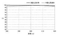
図9は、従来技術で偏光ビームスプリッタ27として用いられる偏光ビームスプリッタの特性の一例を示す図である。図9には、580nm以上620nm以下の波長の光に対する偏光ビームスプリッタのS偏光反射率(S偏光に対する反射率)及びP偏光透過率(P偏光に対する透過率)を示している。また、図9では、横軸は波長[nm]を示し、縦軸は反射率及び透過率[%]を示している。図9を参照するに、580nm以上620nm以下のような波長帯域の幅が狭い、具体的には、40nm程度である場合には、S偏光反射率及びP偏光透過率の双方が98%以上となっている。この場合、偏光ビームスプリッタは、非常に高い精度でS偏光とP偏光とを分離(分岐)することができる。
FIG. 9 is a diagram showing an example of characteristics of a polarization beam splitter used as the
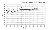
図10は、450nm以上950nm以下の波長の光に対する図9に示す偏光ビームスプリッタの特性の一例、具体的には、S偏光反射率及びP偏光反射率を示す図である。図10では、横軸は波長[nm]を示し、縦軸は反射率及び透過率[%]を示している。図10を参照するに、450nm以上950nm以下のような波長帯域の幅が広い場合には、650nm以上の長波長側でS偏光反射率が急激に低下し、550nm以下の短波長側でP偏光透過率が急激に低下している。これは、580nm以上620nm以下のような狭い波長帯域に対して設計(最適化)された偏光ビームスプリッタであるため、それ以外の波長帯域では、S偏光とP偏光とを分離できないことを示している。 FIG. 10 is a diagram showing an example of characteristics of the polarization beam splitter shown in FIG. 9 with respect to light having a wavelength of 450 nm or more and 950 nm or less, specifically, S polarization reflectance and P polarization reflectance. In FIG. 10, the horizontal axis represents wavelength [nm] and the vertical axis represents reflectance and transmittance [%]. Referring to FIG. 10, when the width of the wavelength band such as 450 nm or more and 950 nm or less is wide, the S-polarized light reflectance sharply decreases on the long wavelength side of 650 nm or more and the P-polarized light on the short wavelength side of 550 nm or less. The transmittance drops sharply. Since this is a polarization beam splitter designed (optimized) for a narrow wavelength band such as 580 nm or more and 620 nm or less, it is shown that S polarization and P polarization cannot be separated in other wavelength bands. There is.
近年では、上述したように、可視光以外の青波長の光や赤外光までを含む広帯域な波長の光をアライメントに用いる必要性が高まっている。しかしながら、図10に示したように、狭い波長帯域に対して最適化された偏光ビームスプリッタを、青波長の光や赤外光に対して用いることはできない。 In recent years, as described above, there is an increasing need to use light having a wide wavelength range including blue light and infrared light other than visible light for alignment. However, as shown in FIG. 10, a polarization beam splitter optimized for a narrow wavelength band cannot be used for blue wavelength light or infrared light.
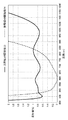
そこで、青波長や赤外波長までを含む広い波長帯域に対して設計(最適化)された偏光ビームスプリッタを用いる必要がある。図11は、450nm以上950nm以下の広い波長帯域に対して設計された偏光ビームスプリッタの特性の一例を示す図である。図11では、横軸は波長[nm]を示し、縦軸は反射率及び透過率[%]を示している。図11を参照するに、図10で見られた650nm以上の長波長側でのS偏光反射率の急激な低下や550nm以下の短波長側でのP偏光透過率の急激な低下がなくなり、広い波長帯域でS偏光が反射し、P偏光が透過していることがわかる。一方、580nm以上620nm以下の波長帯域では98%以上であったS偏光反射率及びP偏光透過率が95%近傍にまで大きく低下している。これは、広い波長帯域に対して偏光ビームスプリッタを設計(膜設計)すると、S偏光反射率及びP偏光透過率を100%に近づけるのが困難になるためである。このように、ブロードな波長特性(膜特性)とS偏光反射率及びP偏光透過率の絶対値とは、トレードオフの関係にある。一般的に、ブロードな波長特性を実現しようとすると膜の層数を増やす必要があり、膜の層数を増やすと膜の吸収が増えたり、多層膜間での干渉による光量ロスが発生したりするため、S偏光反射率やP偏光透過率の絶対値が低下する傾向にある。また、P偏光透過率には、図11に示すように、周期的なうねりのような成分が現れているが、かかる成分も膜の層数を増やしたために起こる現象である。 Therefore, it is necessary to use a polarization beam splitter designed (optimized) for a wide wavelength band including blue wavelengths and infrared wavelengths. FIG. 11 is a diagram showing an example of characteristics of a polarization beam splitter designed for a wide wavelength band of 450 nm or more and 950 nm or less. In FIG. 11, the horizontal axis represents wavelength [nm] and the vertical axis represents reflectance and transmittance [%]. Referring to FIG. 11, the sharp decrease in S-polarized light reflectance on the long wavelength side of 650 nm or more and the sharp decrease of P-polarized light transmittance on the short wavelength side of 550 nm or less seen in FIG. It can be seen that S-polarized light is reflected and P-polarized light is transmitted in the wavelength band. On the other hand, in the wavelength band of 580 nm or more and 620 nm or less, the S-polarized reflectance and the P-polarized transmittance, which were 98% or more, are greatly reduced to around 95%. This is because if the polarization beam splitter is designed (film design) for a wide wavelength band, it becomes difficult to bring the S-polarized reflectance and the P-polarized transmittance close to 100%. Thus, the broad wavelength characteristics (film characteristics) and the absolute values of the S-polarized reflectance and the P-polarized transmittance have a trade-off relationship. Generally, it is necessary to increase the number of layers of the film in order to achieve broad wavelength characteristics, and if the number of layers of the film is increased, absorption of the film increases, and light amount loss due to interference between multilayer films occurs. Therefore, the absolute values of S-polarized reflectance and P-polarized transmittance tend to decrease. Further, as shown in FIG. 11, a component such as a periodic waviness appears in the P-polarized light transmittance, but this component is also a phenomenon caused by increasing the number of layers of the film.
S偏光反射率やP偏光透過率の絶対値が低下したり、周期的なうねりが現れたりする現象は、偏光ビームスプリッタ以外の光学部材でも生じる。図12は、レンズなどの光学部材に用いられる反射防止膜(AR(Anti Reflection)膜)の特性の一例を示す図である。図12では、横軸は波長[nm]を示し、縦軸は反射率[%]を示している。広帯域AR膜特性53は、450nm以上950nm以下の広い波長帯域に対して設計された8層構造のAR膜の特性を示している。また、狭帯域AR膜特性54は、580nm以上620nm以下の狭い波長帯域に対して設計された3層構造のAR膜の特性を示している。 The phenomenon that the absolute values of the S-polarized light reflectance and the P-polarized light transmittance decrease or that the periodic undulation appears appears also in optical members other than the polarization beam splitter. FIG. 12 is a diagram showing an example of characteristics of an antireflection film (AR (Anti Reflection) film) used for an optical member such as a lens. In FIG. 12, the horizontal axis represents wavelength [nm] and the vertical axis represents reflectance [%]. The broadband AR film characteristic 53 indicates the characteristic of an AR film having an 8-layer structure designed for a wide wavelength band of 450 nm or more and 950 nm or less. Further, the narrow band AR film characteristic 54 indicates the characteristic of the three-layer structure AR film designed for a narrow wavelength band of 580 nm or more and 620 nm or less.
図12を参照するに、狭帯域AR膜特性54は、580nm以上620nm以下の波長帯域で反射率が0.2%以下に抑えられている。一方、広帯域AR膜特性53は、450nm以上950nm以下の波長帯域での反射率が0.8%から1.0%程度にしか抑えられていない。これは、偏光ビームスプリッタの特性と同様に、ブロードな波長特性(膜特性)と反射率の絶対値とがトレードオフの関係にあり、両立しないことを示している。これも、AR膜の層数を増やしたことによる膜の吸収や多層膜間での干渉による光量ロスが原因である。また、広帯域AR膜特性53では、狭帯域AR膜特性54と比べて、周期的なうねりも現れている。また、λ/4板30などの位相板も広い波長帯域に対して優れた特性を実現することは困難であるため、偏光ビームスプリッタやAR膜と同様な問題が生じる。
Referring to FIG. 12, in the narrow band AR film characteristic 54, the reflectance is suppressed to 0.2% or less in the wavelength band of 580 nm or more and 620 nm or less. On the other hand, in the broadband AR film characteristic 53, the reflectance in the wavelength band of 450 nm or more and 950 nm or less is suppressed to about 0.8% to 1.0%. This indicates that, like the characteristic of the polarization beam splitter, the broad wavelength characteristic (film characteristic) and the absolute value of the reflectance are in a trade-off relationship and are not compatible with each other. This is also due to the absorption of the film by increasing the number of layers of the AR film and the loss of the light amount due to the interference between the multilayer films. Further, in the broadband AR film characteristic 53, periodic undulation appears as compared with the narrow band AR film characteristic 54. Further, since it is difficult for a phase plate such as the λ/4
このように、アライメントで用いる波長帯域を広げれば広げるほど、偏光ビームスプリッタや位相板などの各種光学部材、及び、AR膜などの膜の設計(製造)の難易度が上がり、それらの特性が低下してしまう。 As described above, the wider the wavelength band used for alignment, the more difficult it is to design (manufacture) various optical members such as a polarization beam splitter and a phase plate, and a film such as an AR film, and their characteristics deteriorate. Resulting in.
図13を参照して、図11に示す特性を有する偏光ビームスプリッタや図12に示す特性を有するAR膜を基板アライメント計測系16に用いた場合に生じる問題について説明する。図13は、基板アライメント計測系16の偏光ビームスプリッタ27の近傍の構成を示す概略図である。
With reference to FIG. 13, a problem that occurs when the polarization beam splitter having the characteristics shown in FIG. 11 or the AR film having the characteristics shown in FIG. 12 is used in the substrate
光源20から射出される光は、図13に示すように、無偏光であり、S偏光とP偏光とを同じ量含んでいる。従って、S偏光100%及びP偏光100%の光が偏光ビームスプリッタ27に導光される。偏光ビームスプリッタ27は、図11に示す特性、即ち、S偏光に対する反射率がP偏光に対する反射率よりも高い反射型偏光子であるため、S偏光を100%反射することはできず、基板側に95%のみ反射される。この際、偏光ビームスプリッタ27は、P偏光も基板側に5%反射してしまう。一方、P偏光95%及びS偏光5%は偏光ビームスプリッタ27を透過するが、偏光ビームスプリッタ27の光源20とは反対側の面には傾斜が設けられているため、かかる面からの反射光が戻ってこないようになっている。
As shown in FIG. 13, the light emitted from the
偏光ビームスプリッタ27で基板側に反射されたS偏光95%及びP偏光5%は、偏光ビームスプリッタ27とλ/4板30との間に配置されたAFプリズム29を透過し、対物レンズ31を介して、基板3を照明する。ここで、図12に示す特性を有するAR膜がAFプリズム29の表面に形成されているとすると、光源20から射出される光の波長帯にもよるが最大で1.0%程度の表面反射がAFプリズム29で発生する。従って、S偏光95%及びP偏光5%の1%がAFプリズム29で反射され、基板3に到達せずに、光電変換素子37に到達する。換言すれば、入射光量をS偏光とP偏光との合計で200%とすると、S偏光0.95%とP偏光0.05%との合計である1.0%が基板3を照明せずに、光電変換素子37に直接到達するフレア光となる。入射光量に対するフレア光量の比(フレア率)は、1.0%/200%=0.5%である。但し、アライメントに暗視野照明を用いる場合、或いは、プロセスウエハの吸収率が高い場合には、信号強度が低いため、アライメント信号がフレア光に埋もれてしまう。
The S-polarized light 95% and the P-polarized light 5% reflected by the
ここで、図14を参照して、暗視野照明の原理について説明する。図14は、開口絞り板24と開口絞り34との関係を中心に基板アライメント計測系16を簡略化して示している。暗視野照明では、基板3に設けられたアライメントマーク19に対して斜入射で光を照射し、アライメントマーク19からの0次回折光を検出せずに、アライメントマーク19からの高次回折光や散乱光などを検出する。アライメントマーク19に対して斜入射で光を照射するために、開口絞り板24に設けられた開口絞りから、輪帯形状で中心部分に遮光部が設けられ、かかる遮光部の周辺部分に光透過部が設けられた開口絞りを選択する。また、開口絞り34には、アライメントマーク19からの0次回折光を検出せずに、高次回折光や散乱光を検出するための開口絞りを用いる。具体的には、開口絞り34として、中心部分に光透過部が設けられ、かかる光透過部の周辺部分に遮光部が設けられた開口絞り、即ち、開口絞り板24で選択した開口絞りの遮光部とは排他的な位置に遮光部が設けられた開口絞りを用いる。
Here, the principle of dark field illumination will be described with reference to FIG. FIG. 14 shows the substrate
暗視野照明では、アライメントマーク19からの0次回折光を検出しないため、アライメントマーク19が設けられていない非マーク部などの段差がない平坦部からは高次回折光や散乱光を検出することができず、平坦部からの信号強度がゼロとなる。換言すれば、暗視野照明では、平坦部からの信号強度がゼロとなるために、アライメントマーク19以外の部分が暗くなる。
In dark-field illumination, the 0th-order diffracted light from the
平坦部からの信号強度がゼロであるのに対して、アライメントマーク19からは、高次回折光や散乱光など弱いながらも信号強度がある。従って、基板アライメント計測系16においてフレア光を小さく抑えることができれば、アライメント信号(マーク信号)のみが得られ、高コントラストを実現することができる。一方、暗視野照明では、アライメント信号に0次回折光が含まれていないため、アライメント信号の強度が低く、アライメント信号を検出可能なレベルまで光量(照明光量)を上げる必要がある。但し、光量を上げると、基板アライメント計測系16で発生するフレア光によってコントラストが低下してしまう。
The signal intensity from the flat portion is zero, whereas the
図15は、基板アライメント計測系16でフレア光が発生しない場合に得られる理想的なアライメント信号の波形を示す図である。図15を参照するに、アライメントマーク19からの信号強度が強く、ベースにはフレア光が乗っていないため、その強度はゼロである。暗視野照明では、アライメント信号の強度は絶対値としては小さいが、光量を上げたり、光電変換素子37の蓄積時間を延ばしたりすることで、ベースにフレア光が乗っていなければ、信号強度としては大きくなる。なお、図15では、アライメント信号の強度を1で規格化している。
FIG. 15 is a view showing a waveform of an ideal alignment signal obtained when the substrate
図16は、基板アライメント計測系16でアライメント信号の強度の半分に相当するフレア光が発生した場合に得られるアライメント信号の波形を示す図である。図16を参照するに、理想的なアライメント信号と比べると、アライメントマーク19からの規格化された信号強度は1で同じであるが、フレア光による信号強度がある(フレア強度が0.5である)ため、ベースの信号強度が上がっている。
FIG. 16 is a diagram showing a waveform of the alignment signal obtained when the substrate
コントラストは、一般的に、アライメント信号の強度からベースの信号強度を差し引いた値で評価される。従って、図15に示すアライメント信号のコントラストは、(アライメント信号の強度1)−(ベースの信号強度0)で1となるが、図16に示すアライメント信号のコントラストは、(アライメント信号の強度1)−(ベースの信号強度0.5)で0.5となる。 Contrast is generally evaluated by the value of the alignment signal strength minus the base signal strength. Therefore, the contrast of the alignment signal shown in FIG. 15 is 1 by (alignment signal intensity 1)−(base signal intensity 0), but the contrast of the alignment signal shown in FIG. 16 is (alignment signal intensity 1). -(Base signal strength 0.5) is 0.5.
コントラストは高ければ高いほど計測に有利であるため、暗視野照明では、一般的に、アライメント信号の強度を1とすると、ベースの信号強度を0.3以下に抑える必要がある。ベースの信号強度が0.3を超えると、計測エラーが発生したり、計測ができたとしても、プロセスばらつきなどで基板内での信号強度にばらつきが生じ、計測精度が低下したりする。 Since the higher the contrast is, the more advantageous the measurement is, in dark field illumination, generally, when the intensity of the alignment signal is 1, it is necessary to suppress the signal intensity of the base to 0.3 or less. When the signal intensity of the base exceeds 0.3, a measurement error occurs, or even if measurement can be performed, the signal intensity within the substrate varies due to process variations and the like, and the measurement accuracy deteriorates.
図13に示すように、入射光量に対するフレア率が0.5%である場合、暗視野照明において、アライメントマーク19からの信号強度が0.55%程度と低ければ、図17に示すように、アライメント信号がフレア強度(フレア光)に埋もれてしまう。暗視野照明では、上述したように、アライメントマーク19からの0次回折光を検出せずに、微弱な高次回折光や散乱光などを検出するため、アライメントマーク19からの信号強度が0.55%程度となることがある。アライメントマーク19からの信号強度0.55%に対してフレア率が0.5%である場合、アライメント信号の強度を1とすると、フレア強度が0.9(≒0.5%/0.55%)近くあることを意味する。図17を参照するに、アライメント信号の強度1に対してフレア強度が0.9もあり、ベースの信号強度が暗視野照明のターゲット(閾値)である0.3を大きく超えている。
As shown in FIG. 13, when the flare ratio with respect to the amount of incident light is 0.5% and the signal intensity from the
このように、入射光量に対するフレア率が高い場合(図13に示す基板アライメント計測系16)では、アライメント信号の強度が低いと、計測精度が低下したり、計測エラーが発生したりする可能性が高くなる。従って、基板アライメント計測系16で発生するフレア光を低減(抑制)することが重要である。
As described above, in the case where the flare rate with respect to the incident light amount is high (the substrate
そこで、本実施形態では、広帯域な波長の光を用いながら、基板アライメント計測系16で発生するフレア光を低減することを実現する技術を提供する。図18は、本実施形態における基板アライメント計測系16の偏光ビームスプリッタ27の近傍の構成を示す概略図である。基板アライメント計測系16は、本実施形態では、図18に示すように、照明系ILに偏光子55を含む。偏光子55は、本実施形態では、S偏光に対する透過率がP偏光に対する透過率よりも高く、具体的には、S偏光のみを100%透過し、P偏光に対する透過率を1%に抑えた透過型偏光子である。偏光子55は、例えば、偏光ビームスプリッタやワイヤーグリッドなどで構成されている。
In view of this, the present embodiment provides a technique for reducing flare light generated in the substrate
光源20から射出される光は、図18に示すように、無偏光であり、S偏光とP偏光とを同じ量含んでいる。従って、S偏光100%及びP偏光100%の光が偏光子55に導光される。偏光子55は、上述したように、S偏光に対する透過率が100%であり、P偏光に対する透過率が1%であるため、S偏光100%及びP偏光1%が偏光子55を透過して、偏光ビームスプリッタ27に到達する。偏光ビームスプリッタ27は、図11に示す特性、即ち、S偏光に対する反射率がP偏光に対する反射率よりも高い反射型偏光子であるため、S偏光を100%反射することはできず、S偏光が基板側に95%のみ反射され、P偏光も基板側に5%反射される。従って、S偏光95%とP偏光0.05%とが偏光ビームスプリッタ27とλ/4板30との間に配置されたAFプリズム29に到達する。
As shown in FIG. 18, the light emitted from the
AFプリズム29は、AR膜が設けられた透過部材である。本実施形態では、AFプリズム29の表面には、図12に示す特性を有するAR膜が形成されているため、上述したように、1.0%程度の表面反射がAFプリズム29で発生する。従って、S偏光の0.95%及びP偏光の0.0005%がAFプリズム29で反射され、基板3に到達せずに、光電変換素子37に到達する。換言すれば、S偏光0.95%とP偏光0.0005%との合計である0.9505%が基板3を照明せずに、光電変換素子37に直接到達するフレア光となる。入射光量に対するフレア率は、本実施形態では、0.47525%である。このように、本実施形態では、入射光量に対するフレア率が図13に示す基板アライメント計測系16におけるフレア率(5%)よりも改善している。従って、偏光子55は、偏光ビームスプリッタ27で反射されるP偏光の影響を低減することに効果がある。
The
図19は、本実施形態における基板アライメント計測系16の偏光ビームスプリッタ27の近傍の別の構成を示す概略図である。基板アライメント計測系16は、本実施形態では、図19に示すように、照明系ILに偏光子55を含むことに加えて、更に、結像系IMに偏光子56を含む。偏光子56は、本実施形態では、P偏光に対する透過率がS偏光に対する透過率よりも高く、具体的には、P偏光のみを100%透過し、S偏光に対する透過率を1%に抑えた透過型偏光子である。偏光子56は、例えば、偏光ビームスプリッタやワイヤーグリッドなどで構成されている。偏光子55と偏光子56とは、透過する偏光軸が光学的に直交している。
FIG. 19 is a schematic diagram showing another configuration in the vicinity of the
光源20から射出される光は、図19に示すように、無偏光であり、S偏光とP偏光とを同じ量含んでいる。従って、S偏光100%及びP偏光100%の光が偏光子55に導光される。偏光子55は、上述したように、S偏光に対する透過率が100%であり、P偏光に対する透過率が1%であるため、S偏光100%及びP偏光1%が偏光子55を透過して、偏光ビームスプリッタ27に到達する。偏光ビームスプリッタ27は、図11に示す特性、即ち、S偏光に対する反射率がP偏光に対する反射率よりも高い反射型偏光子であるため、S偏光を100%反射することはできず、S偏光が基板側に95%のみ反射され、P偏光も基板側に5%反射される。従って、S偏光95%とP偏光0.05%とが偏光ビームスプリッタ27とλ/4板30との間に配置されたAFプリズム29に到達する。
As shown in FIG. 19, the light emitted from the
AFプリズム29は、AR膜が設けられた透過部材である。本実施形態では、AFプリズム29の表面には、図12に示す特性を有するAR膜が形成されているため、上述したように、1.0%程度の表面反射がAFプリズム29で発生する。従って、S偏光の0.95%及びP偏光の0.0005%がAFプリズム29で反射され、基板3に到達せずに、結像系側に反射される。
The
結像系側に反射されたS偏光0.95%及びP偏光0.0005%は、偏光子56に到達する。偏光子56は、上述したように、P偏光に対する透過率が100%であり、S偏光に対する透過率が1%であるため、S偏光0.0095%及びP偏光0.0005%が偏光子56を透過して、光電変換素子37に到達する。従って、S偏光0.0095%とP偏光0.0005%との合計である0.01%が基板3を照明せずに、光電変換素子37に直接到達するフレア光となる。入射光量に対するフレア率は、本実施形態では、0.005%である。このように、本実施形態では、入射光量に対するフレア率が図13に示す基板アライメント計測系16におけるフレア率(5%)の1/100にまで改善している。従って、偏光子56は、偏光ビームスプリッタ27を透過するS偏光の影響を低減することに効果がある。
0.95% of S-polarized light and 0.0005% of P-polarized light reflected to the image forming system side reach the
暗視野照明において、アライメントマーク19からの信号強度が0.55%程度と低い場合、上述したように、フレア率が0.5%である(図13)と、図17に示すように、アライメント信号がフレア強度に埋もれてしまう。但し、図18や図19に示す本実施形態では、このようなアライメント信号がフレア強度に埋もれてしまうことを改善することができる。例えば、図19に示す本実施形態では、アライメントマーク19からの信号強度が0.55%であっても、フレア率が0.005%と低減しているため、図20に示すようなアライメント信号が得られる。図20は、図19に示す基板アライメント計測系16で得られるアライメント信号の波形を示す図である。アライメントマーク19からの信号強度0.55%に対してフレア率が0.05%であることは、アライメント信号の強度を1とすると、フレア強度は0.01(≒0.005%/0.55%)程度であることを意味する。図20を参照するに、アライメント信号の強度1に対してフレア強度が0.01程度であり、ベースの信号強度が暗視野照明のターゲット(閾値)である0.3以下となっている。
In the dark field illumination, when the signal intensity from the
本実施形態では、偏光ビームスプリッタ27とλ/4板30との間に少なくとも1つの光学部材(例えば、AFプリズム29)を有する基板アライメント計測系16において、照明系IL、或いは、照明系IL及び結像系IMが偏光子を含む。これにより、基板アライメント計測系16で得られるアライメント信号のコントラストを大幅に改善することができる。
In the present embodiment, in the substrate
また、本実施形態では、アライメント信号のコントラストが改善すると説明したが、これは、アライメントマーク19からの信号強度がより低いプロセスでもアライメントマーク19が検出可能であることも意味する。例えば、暗視野照明でのベースの信号強度のターゲットである0.3以下を実現するために、図13に示す基板アライメント計測系16では、フレア率が0.5%であるため、アライメント信号の強度が1.6%(≒0.5/(1/0.3))程度必要となる。一方、図19に示す基板アライメント計測系16では、フレア率が0.05%であるため、アライメント信号の強度が0.016%(≒0.005/(1/0.3))程度であっても、アライメントマーク19が検出可能となる。換言すれば、図19に示す基板アライメント計測系16は、図13に示す基板アライメント計測系16と比べて、アライメントマーク19からの信号強度が100倍暗くてもアライメントマーク19を検出することができる。
Further, although it has been described in the present embodiment that the contrast of the alignment signal is improved, this also means that the
なお、図19では、説明を簡単にするために、偏光ビームスプリッタ27の近傍の構成を中心に示したが、基板アライメント計測系16は、実際には、図21に示す構成を有する。図21は、本実施形態における基板アライメント計測系16の具体的な構成を示す概略図である。
Note that, in FIG. 19, the configuration in the vicinity of the
また、これまでの説明では、アライメントマーク19からの信号強度が低い場合の一例として暗視野照明を挙げたが、本実施形態における基板アライメント計測系16は、明視野照明にも採用可能である。
Further, in the above description, dark field illumination is taken as an example in the case where the signal intensity from the
図22を参照して、明視野照明の原理について説明する。図22は、開口絞り板24と開口絞り34との関係を中心に基板アライメント計測系16を簡略化して示している。明視野照明では、暗視野照明で用いた開口絞りとは異なる開口絞りを用いる(即ち、開口絞りを切り換える)。
The principle of bright field illumination will be described with reference to FIG. FIG. 22 shows the substrate
明視野照明では、基板3に設けられたアライメントマーク19に対して垂直入射で光を照射して、アライメントマーク19からの0次回折光も検出するため、暗視野照明と比べて、アライメントマーク19からの光量が高い。一方、アライメントマーク19が設けられていない非マーク部などの段差がない平坦部からの0次回折光も検出してしまうため、平坦部からの光量も高い。従って、明視野照明では、アライメント信号のコントラストが暗視野照明よりも低くなる。
In the bright field illumination, the
図23は、明視野照明において得られるアライメント信号の波形の一例を示す図である。図23を参照するに、明視野照明では、上述したように、平坦部からの0次回折光も検出するため、平坦部からの信号強度(平坦部強度)が高くなっている。図24は、明視野照明において、基板アライメント計測系16でフレア光が発生した場合に得られるアライメント信号の波形を示す図である。図24を参照するに、アライメント信号とは別のフレア強度が平坦部強度(ベース)に追加されるため、アライメント信号の強度が相対的に低減して、コントラストが低下している。明視野照明であっても、プロセスウエハの吸収率が高いと、アライメントマーク19からの光量と平坦部からの光量とがともに低下するため、基板アライメント計測系16で発生するフレア光を低減しなければ、フレア光の影響が相対的に高くなる。これにより、図24に示すように、アライメント信号のコントラストが低下してしまう。従って、暗視野照明や明視野照明に関わらず、基板アライメント計測系16で発生するフレア光を低減することは重要である。
FIG. 23 is a diagram showing an example of a waveform of an alignment signal obtained in bright field illumination. Referring to FIG. 23, in bright-field illumination, as described above, the 0th-order diffracted light from the flat portion is also detected, so the signal intensity from the flat portion (flat portion intensity) is high. FIG. 24 is a diagram showing a waveform of an alignment signal obtained when flare light is generated in the substrate
本実施形態では、主に、図19及び図21に示すように、基板アライメント計測系16の照明系IL及び結像系IMのそれぞれが偏光子を含んでいる場合を例に説明した。但し、図18に示すように、基板アライメント計測系16の照明系ILのみが偏光子を含んでいる場合であっても、基板アライメント計測系16で発生するフレア光を低減することができる。また、基板アライメント計測系16の結像系IMのみが偏光子を含んでいる場合であっても、基板アライメント計測系16で発生するフレア光を低減することができる。このように、基板アライメント計測系16において、照明系IL及び結像系IMの少なくとも一方が偏光子を含んでいればよい。
In this embodiment, as shown in FIGS. 19 and 21, the case where each of the illumination system IL and the imaging system IM of the substrate
また、本実施形態では、偏光ビームスプリッタ27とλ/4板30との間に配置された少なくとも1つの光学部材として、AFプリズム29を例に説明したが、これに限定されるものではない。例えば、図25に示すように、偏光ビームスプリッタ27とλ/4板30との間に配置された少なくとも1つの光学部材は、全反射プリズム57であってもよい。図25は、偏光ビームスプリッタ27とλ/4板30との間に全反射プリズム57が配置された基板アライメント計測系16の偏光ビームスプリッタ27の近傍の構成を示す概略図である。
Further, in the present embodiment, the
全反射プリズム57は、光学系の光軸(光線)を折り曲げるミラー(反射部材)の1種である。全反射プリズム57は、全反射プリズム57の斜辺と空気層との屈折率差で生じる全反射効果によって、光量ロスなく、光の向きを90度回転させる。一般的な表面反射ミラーには、アルミなどの金属膜が形成(コーティング)されているため、かかる表面反射ミラーの反射率は、90%程度となり、光量を10%程度ロスしてしまう。従って、全反射プリズム57は、光量的に、即ち、光量ロスなく光を回転させる上で有利である。但し、全反射プリズム57には、偏光ビームスプリッタ27で反射された光が全反射プリズム57の硝材の表面に設けられたAR膜で反射されることでフレア光となる問題がある。このように、偏光ビームスプリッタ27とλ/4板30との間に全反射プリズム57を配置した場合にも、基板アライメント計測系16ではフレア光が発生する。従って、上述したように、基板アライメント計測系16の照明系IL及び結像系IMの少なくとも一方に偏光子を設けることで、基板アライメント計測系16で発生するフレア光を低減することができる。
The
本実施形態では、偏光ビームスプリッタ27とλ/4板30との間に、1つのAFプリズム29、或いは、1つの全反射プリズム57が配置されている場合を例に説明したが、これに限定されるものではない。例えば、AFプリズム29と全反射プリズム57とを、偏光ビームスプリッタ27とλ/4板30との間に配置してもよい。このように、偏光ビームスプリッタ27とλ/4板30との間には、複数の光学部材が配置されてもよい。
In the present embodiment, the case where one
また、本実施形態では、偏光ビームスプリッタ27をプリズムタイプで図示しているが、偏光ビームスプリッタ27は、平行平板を45度傾けて配置するミラータイプであってもよい。
Further, in the present embodiment, the
また、基板アライメント計測系16において、照明系ILに含まれる偏光子55は、図26に示すように、照明系ILの光軸に対して傾けて配置されているとよい。同様に、結像系IMに含まれる偏光子56は、図26に示すように、結像系IMの光軸に対して傾けて配置されているとよい。図26は、本実施形態における基板アライメント計測系16の偏光ビームスプリッタ27の近傍の構成を示す概略図である。
Further, in the substrate
照明系ILに含まれる偏光子55を光軸に対して傾けて配置することで、偏光子55の表面で反射される光を光軸から斜めに向けることができる。例えば、偏光子55は、P偏光を1%しか透過させないため、99%のP偏光は、偏光子55で反射される。ここで、偏光子55を光軸に対して傾けずに垂直に配置すると、偏光子55で反射された99%のP偏光が光源20に戻り、光源20で反射され、偏光子55に再度到達して透過することになるため、フレア光となってしまう。このようなフレア光は、微少量であり、通常は無視することができるが、より高精度なアライメントを実現するためには、このようなフレア光の影響も低減する必要がある。図26に示すように、偏光子55を光軸に対して傾けて配置することで、偏光子55で反射された99%のP偏光は、光源20に戻らず(即ち、光源20で反射されず)、偏光子55に再度到達することを防止することができる。換言すれば、偏光子55で反射された99%のP偏光からフレア光が発生することを防止することができる。
By arranging the
同様に、結像系IMに含まれる偏光子56を光軸に対して傾けずに垂直に配置すると、偏光子56で反射された99%のS偏光がAFプリズム29の表面で反射され、偏光子56に再度到達して透過することになるため、フレア光となってしまう。図26に示すように、偏光子56を光軸に対して傾けて配置することで、偏光子56で反射された99%のS偏光は、AFプリズム29に戻らず(即ち、AFプリズム29の表面で反射されず)、偏光子56に再度到達することを防止することができる。換言すれば、偏光子56で反射された99%のS偏光からフレア光が発生することを防止することができる。
Similarly, when the
このように、照明系ILに含まれる偏光子55及び結像系IMに含まれる偏光子56のそれぞれを光軸に対して傾けて配置することは、基板アライメント計測系16で発生するフレア光を低減する上で有効である。また、偏光子55及び56のそれぞれを傾ける方向(回転方向)は、透過軸に対して直交する方向を回転軸とし、照明系ILと結像系IMとで直交させるとよい。
As described above, arranging each of the
また、偏光子55及び56は、図21に示すように、基板3と光学的に共役な面(共役面)58からシフトした面(位置)に配置されている。偏光子55及び56は、その性能を考慮すると、基本的には、入射光が角度を有していない面に配置するとよい。偏光子55及び56は、垂直入射光に対して所定の偏光のみを透過する特性を有する光学素子であるが、入射光が角度を有していると、所定外の偏光も透過する懸念がある。
Further, as shown in FIG. 21, the
基板アライメント計測系16の照明系ILでは、第1照明系25と第2照明系26との間や第1コンデンサ光学系21と第2コンデンサ光学系23との間に、光が角度を有していない領域、即ち、共役面58が存在する。但し、偏光子55を共役面58に配置すると、偏光子55の表面に存在するキズやゴミなどが基板3に写り込み、計測だまされとなる可能性がある。従って、偏光子55は、第1照明系25と第2照明系26との間又は第1コンデンサ光学系21と第2コンデンサ光学系23との間であって、共役面58を避けて配置するとよい。本実施形態では、図21に示すように、第1コンデンサ光学系21と第2コンデンサ光学系23との間であって、共役面58からシフトした面に偏光子55を配置している。
In the illumination system IL of the substrate
一方、基板アライメント計測系16の結像系IMでは、第1結像系33と第2結像系35との間や光電変換素子37の入射面に共役面58が存在する。従って、偏光子56は、図21に示すように、光が角度を有しておらず、且つ、共役面58を避けることが可能な第1結像系33と第2結像系35との間に配置するとよい。なお、対物レンズ31とリレーレンズ32との間も光が角度を有しておらず、且つ、共役面58を避けることができるが、偏光ビームスプリッタ27、AFプリズム29、λ/4板30などの複数の光学部材が既に配置されている。そこで、本実施形態では、第1結像系33と第2結像系35との間に偏光子56を配置することで、共役面58から偏光子56をシフトさせて配置している。これにより、偏光子56の像が光電変換素子37(基板3)に写り込むことなく、良好な計測が可能となる。
On the other hand, in the image formation system IM of the substrate
このように、照明系ILに含まれる偏光子55及び結像系IMに含まれる偏光子56のそれぞれを共役面58からシフトさせて配置することは、偏光子55及び56による計測精度の低下を抑制して良好な計測を実現する上で有効である。
As described above, arranging each of the
また、本実施形態では、偏光ビームスプリッタ27を、S偏光に対する反射率がP偏光に対する反射率よりも高い反射型偏光子として説明した。但し、偏光ビームスプリッタ27を、P偏光に対する反射率がS偏光に対する反射率よりも高い反射型偏光子に置換することもできる。この場合、照明系ILに含まれる偏光子55をP偏光に対する透過率がS偏光に対する透過率よりも高い透過型偏光子とし、結像系IMに含まれる偏光子56をS偏光に対する透過率がP偏光に対する透過率よりも高い透過型偏光子とすればよい。
Further, in the present embodiment, the
本実施形態における基板アライメント計測系16によれば、フレア光を低減し、アライメント信号のコントラストを大幅に改善することができるため、計測精度が向上し、基板3の位置を高精度に求めることができる。従って、基板アライメント計測系16を有する露光装置100は、レチクル1と基板3とのアライメントにおいて、高精度なオーバーレイ精度を達成することができる。
According to the substrate
本発明の実施形態における物品の製造方法は、例えば、デバイス(半導体素子、磁気記憶媒体、液晶表示素子など)、カラーフィルタ、光学部品、MEMSなどの物品を製造するのに好適である。かかる製造方法は、上述した実施形態の露光装置100を用いて、感光剤が塗布された基板を露光する工程と、露光された感光剤を現像する工程とを含む。また、現像された感光剤のパターンをマスクとして基板に対してエッチング工程やイオン注入工程などを行い、基板上に回路パターンが形成される。これらの露光、現像、エッチングなどの工程を繰り返して、基板上に複数の層からなる回路パターンを形成する。後工程で、回路パターンが形成された基板に対してダイシング(加工)を行い、チップのマウンティング、ボンディング、検査工程を行う。また、かかる製造方法は、他の周知の工程(酸化、成膜、蒸着、ドーピング、平坦化、レジスト剥離など)を含みうる。本実施形態における物品の製造方法は、従来に比べて、物品の性能、品質、生産性及び生産コストの少なくとも1つにおいて有利である。
The method of manufacturing an article according to the embodiment of the present invention is suitable for manufacturing an article such as a device (semiconductor element, magnetic storage medium, liquid crystal display element, etc.), color filter, optical component, or MEMS. Such a manufacturing method includes a step of exposing the substrate coated with the photosensitive agent and a step of developing the exposed photosensitive agent using the
発明は上記実施形態に制限されるものではなく、発明の精神及び範囲から離脱することなく、様々な変更及び変形が可能である。従って、発明の範囲を公にするために請求項を添付する。 The invention is not limited to the above-described embodiments, and various changes and modifications can be made without departing from the spirit and scope of the invention. Therefore, the following claims are attached to open the scope of the invention.
100:露光装置 27:偏光ビームスプリッタ 29:AFプリズム 30:λ/4板 37:光電変換素子 55、56:偏光子 IL:照明系 IM:結像系 DS:分離系
100: Exposure device 27: Polarization beam splitter 29: AF prism 30: λ/4 plate 37:
Claims (15)
前記被検物体を照明光で照明する照明系と、
前記被検物体からの検出光を、前記被検物体の像を検出する光電変換素子に結像する結像系と、
前記照明系と前記結像系との間に配置された反射型偏光子及びλ/4板とを含み、前記反射型偏光子及び前記λ/4板を介して前記照明光と前記検出光とを分離する分離系と、
を有し、
前記分離系は、前記反射型偏光子と前記λ/4板との間に配置された少なくとも1つの光学部材を含み、
前記照明系及び前記結像系の少なくとも一方は、偏光子を含むことを特徴とする計測装置。 A measuring device for measuring the position of an object to be inspected,
An illumination system that illuminates the test object with illumination light,
An imaging system that forms the detection light from the object to be detected on a photoelectric conversion element that detects an image of the object to be detected,
A reflection type polarizer and a λ/4 plate disposed between the illumination system and the image forming system, and the illumination light and the detection light through the reflection type polarizer and the λ/4 plate. A separation system that separates
Have
The separation system includes at least one optical member arranged between the reflective polarizer and the λ/4 plate,
At least one of the illumination system and the imaging system includes a polarizer.
前記反射型偏光子は、S偏光に対する反射率がP偏光に対する反射率よりも高く、
前記照明系に含まれる前記偏光子は、S偏光に対する透過率がP偏光に対する透過率よりも高く、
前記結像系に含まれる前記偏光子は、P偏光に対する透過率がS偏光に対する透過率よりも高いことを特徴とする請求項2に記載の計測装置。 Each of the illumination system and the imaging system includes a polarizer,
In the reflective polarizer, the reflectance for S-polarized light is higher than the reflectance for P-polarized light,
The polarizer included in the illumination system has a transmittance for S-polarized light higher than that for P-polarized light,
The measuring device according to claim 2, wherein the polarizer included in the imaging system has a transmittance for P-polarized light higher than a transmittance for S-polarized light.
前記結像系に含まれる前記偏光子は、P偏光に対する透過率が100%であり、S偏光に対する透過率が1%であることを特徴とする請求項3に記載の計測装置。 The polarizer included in the illumination system has a transmittance of 100% for S-polarized light and a transmittance of 1% for P-polarized light,
The measuring device according to claim 3, wherein the polarizer included in the imaging system has a transmittance of 100% for P-polarized light and a transmittance of 1% for S-polarized light.
前記反射型偏光子は、P偏光に対する反射率がS偏光に対する反射率よりも高く、
前記照明系に含まれる前記偏光子は、P偏光に対する透過率がS偏光に対する透過率よりも高く、
前記結像系に含まれる前記偏光子は、S偏光に対する透過率がP偏光に対する透過率よりも高いことを特徴とする請求項2に記載の計測装置。 Each of the illumination system and the imaging system includes a polarizer,
In the reflective polarizer, the reflectance for P-polarized light is higher than the reflectance for S-polarized light,
The polarizer included in the illumination system has a transmittance for P-polarized light higher than that for S-polarized light,
The measuring device according to claim 2, wherein the polarizer included in the imaging system has a transmittance for S-polarized light higher than a transmittance for P-polarized light.
前記結像系に含まれる前記偏光子は、前記結像系の光軸に対して傾けて配置されていることを特徴とする請求項1乃至9のうちいずれか1項に記載の計測装置。 The polarizer included in the illumination system is arranged to be inclined with respect to the optical axis of the illumination system,
The measuring device according to any one of claims 1 to 9, wherein the polarizer included in the image forming system is arranged to be inclined with respect to an optical axis of the image forming system.
前記基板を保持するステージと、
前記基板の位置を被検物体の位置として計測する請求項1乃至13のうちいずれか1項に記載の計測装置と、
前記計測装置の計測結果に基づいて、前記ステージの位置を制御する制御部と、
を有することを特徴とする露光装置。 A projection optical system that projects the pattern of the reticle onto the substrate,
A stage for holding the substrate,
The measuring device according to any one of claims 1 to 13, which measures the position of the substrate as the position of the object to be inspected,
A control unit for controlling the position of the stage based on the measurement result of the measuring device;
An exposure apparatus comprising:
露光した前記基板を現像する工程と、
現像された前記基板から物品を製造する工程と、
を有することを特徴とする物品の製造方法。 Exposing a substrate using the exposure apparatus according to claim 14;
Developing the exposed substrate,
Manufacturing an article from the developed substrate,
A method for manufacturing an article, comprising:
Priority Applications (5)
| Application Number | Priority Date | Filing Date | Title |
|---|---|---|---|
| JP2019015987A JP2020122930A (en) | 2019-01-31 | 2019-01-31 | Measurement device, exposure device and manufacturing method of article |
| TW109101290A TW202109215A (en) | 2019-01-31 | 2020-01-15 | Measurement apparatus, exposure apparatus, and method of manufacturing article |
| US16/751,388 US11169452B2 (en) | 2019-01-31 | 2020-01-24 | Measurement apparatus, exposure apparatus, and method of manufacturing article |
| KR1020200009661A KR20200095398A (en) | 2019-01-31 | 2020-01-28 | Measurement apparatus, exposure apparatus, and method of manufacturing article |
| CN202010077600.3A CN111505915A (en) | 2019-01-31 | 2020-01-31 | Measuring apparatus, exposure apparatus, and method of manufacturing article |
Applications Claiming Priority (1)
| Application Number | Priority Date | Filing Date | Title |
|---|---|---|---|
| JP2019015987A JP2020122930A (en) | 2019-01-31 | 2019-01-31 | Measurement device, exposure device and manufacturing method of article |
Publications (2)
| Publication Number | Publication Date |
|---|---|
| JP2020122930A true JP2020122930A (en) | 2020-08-13 |
| JP2020122930A5 JP2020122930A5 (en) | 2022-01-24 |
Family
ID=71836385
Family Applications (1)
| Application Number | Title | Priority Date | Filing Date |
|---|---|---|---|
| JP2019015987A Pending JP2020122930A (en) | 2019-01-31 | 2019-01-31 | Measurement device, exposure device and manufacturing method of article |
Country Status (5)
| Country | Link |
|---|---|
| US (1) | US11169452B2 (en) |
| JP (1) | JP2020122930A (en) |
| KR (1) | KR20200095398A (en) |
| CN (1) | CN111505915A (en) |
| TW (1) | TW202109215A (en) |
Families Citing this family (1)
| Publication number | Priority date | Publication date | Assignee | Title |
|---|---|---|---|---|
| JP7328806B2 (en) * | 2019-06-25 | 2023-08-17 | キヤノン株式会社 | Metrology apparatus, lithographic apparatus, and method of manufacturing an article |
Citations (11)
| Publication number | Priority date | Publication date | Assignee | Title |
|---|---|---|---|---|
| JPS62181431A (en) * | 1987-01-23 | 1987-08-08 | Canon Inc | Automatic aligning apparatus |
| JPH03290916A (en) * | 1990-04-06 | 1991-12-20 | Canon Inc | Mark detector and aligner |
| JPH05341234A (en) * | 1992-06-12 | 1993-12-24 | Chinon Ind Inc | Polarization optical system and liquid crystal projector device |
| JP2004069398A (en) * | 2002-08-02 | 2004-03-04 | Hitachi Electronics Eng Co Ltd | Method and device for detecting alignment, method and equipment for manufacturing device |
| JP2009115515A (en) * | 2007-11-02 | 2009-05-28 | Canon Inc | Position detector, position detection method, exposure apparatus, and method of manufacturing device |
| JP5036429B2 (en) * | 2007-07-09 | 2012-09-26 | キヤノン株式会社 | Position detection apparatus, exposure apparatus, device manufacturing method, and adjustment method |
| JP2013105936A (en) * | 2011-11-15 | 2013-05-30 | Canon Inc | Position detection device and exposure device |
| JP2013187206A (en) * | 2012-03-05 | 2013-09-19 | Canon Inc | Detection device, exposure device, and method for manufacturing device |
| JP2013219086A (en) * | 2012-04-04 | 2013-10-24 | Canon Inc | Detector, lithography device, charged particle beam device, and article manufacturing method |
| JP2014081452A (en) * | 2012-10-16 | 2014-05-08 | Nikon Corp | Exposure apparatus and device manufacturing method |
| JP2019507372A (en) * | 2015-12-30 | 2019-03-14 | コーロン インダストリーズ インク | Wire grid polarizer and optical component including the same |
Family Cites Families (12)
| Publication number | Priority date | Publication date | Assignee | Title |
|---|---|---|---|---|
| JP3350918B2 (en) | 1996-03-26 | 2002-11-25 | 株式会社高岳製作所 | Two-dimensional array confocal optical device |
| JP2002022410A (en) | 2000-07-04 | 2002-01-23 | Canon Inc | Method and apparatus for detecting position |
| US7136159B2 (en) * | 2000-09-12 | 2006-11-14 | Kla-Tencor Technologies Corporation | Excimer laser inspection system |
| US6917421B1 (en) * | 2001-10-12 | 2005-07-12 | Kla-Tencor Technologies Corp. | Systems and methods for multi-dimensional inspection and/or metrology of a specimen |
| JP3878107B2 (en) * | 2002-11-06 | 2007-02-07 | 株式会社日立ハイテクノロジーズ | Defect inspection method and apparatus |
| JP3971363B2 (en) * | 2003-10-07 | 2007-09-05 | 株式会社東芝 | Exposure apparatus and method for measuring Mueller matrix of optical system of exposure apparatus |
| DE102005030543A1 (en) * | 2004-07-08 | 2006-02-02 | Carl Zeiss Smt Ag | Polarizer device for illumination system, has interference device converting light beam with angular distribution to another beam, and decoupling device receiving latter beam and emitting beam with another angular distribution |
| US7446882B2 (en) * | 2005-01-20 | 2008-11-04 | Zygo Corporation | Interferometer for determining characteristics of an object surface |
| JP4723362B2 (en) * | 2005-11-29 | 2011-07-13 | 株式会社日立ハイテクノロジーズ | Optical inspection apparatus and method |
| JP2010133840A (en) | 2008-12-05 | 2010-06-17 | Nokodai Tlo Kk | Shape measuring apparatus and shape measuring method |
| JP6066627B2 (en) * | 2012-08-23 | 2017-01-25 | キヤノン株式会社 | POSITION DETECTING APPARATUS, LITHOGRAPHIC APPARATUS USING SAME, AND DEVICE MANUFACTURING METHOD |
| WO2018210505A1 (en) * | 2017-05-15 | 2018-11-22 | Asml Netherlands B.V. | Metrology sensor, lithographic apparatus and method for manufacturing devices |
-
2019
- 2019-01-31 JP JP2019015987A patent/JP2020122930A/en active Pending
-
2020
- 2020-01-15 TW TW109101290A patent/TW202109215A/en unknown
- 2020-01-24 US US16/751,388 patent/US11169452B2/en active Active
- 2020-01-28 KR KR1020200009661A patent/KR20200095398A/en active Search and Examination
- 2020-01-31 CN CN202010077600.3A patent/CN111505915A/en active Pending
Patent Citations (11)
| Publication number | Priority date | Publication date | Assignee | Title |
|---|---|---|---|---|
| JPS62181431A (en) * | 1987-01-23 | 1987-08-08 | Canon Inc | Automatic aligning apparatus |
| JPH03290916A (en) * | 1990-04-06 | 1991-12-20 | Canon Inc | Mark detector and aligner |
| JPH05341234A (en) * | 1992-06-12 | 1993-12-24 | Chinon Ind Inc | Polarization optical system and liquid crystal projector device |
| JP2004069398A (en) * | 2002-08-02 | 2004-03-04 | Hitachi Electronics Eng Co Ltd | Method and device for detecting alignment, method and equipment for manufacturing device |
| JP5036429B2 (en) * | 2007-07-09 | 2012-09-26 | キヤノン株式会社 | Position detection apparatus, exposure apparatus, device manufacturing method, and adjustment method |
| JP2009115515A (en) * | 2007-11-02 | 2009-05-28 | Canon Inc | Position detector, position detection method, exposure apparatus, and method of manufacturing device |
| JP2013105936A (en) * | 2011-11-15 | 2013-05-30 | Canon Inc | Position detection device and exposure device |
| JP2013187206A (en) * | 2012-03-05 | 2013-09-19 | Canon Inc | Detection device, exposure device, and method for manufacturing device |
| JP2013219086A (en) * | 2012-04-04 | 2013-10-24 | Canon Inc | Detector, lithography device, charged particle beam device, and article manufacturing method |
| JP2014081452A (en) * | 2012-10-16 | 2014-05-08 | Nikon Corp | Exposure apparatus and device manufacturing method |
| JP2019507372A (en) * | 2015-12-30 | 2019-03-14 | コーロン インダストリーズ インク | Wire grid polarizer and optical component including the same |
Also Published As
| Publication number | Publication date |
|---|---|
| TW202109215A (en) | 2021-03-01 |
| US11169452B2 (en) | 2021-11-09 |
| CN111505915A (en) | 2020-08-07 |
| KR20200095398A (en) | 2020-08-10 |
| US20200249589A1 (en) | 2020-08-06 |
Similar Documents
| Publication | Publication Date | Title |
|---|---|---|
| JP6025346B2 (en) | Detection apparatus, exposure apparatus, and device manufacturing method | |
| US9291921B2 (en) | Detection apparatus, exposure apparatus, device fabrication method and filter to reduce a difference between detected intensity values of lights having different wavelength ranges | |
| JP5743958B2 (en) | Measuring method, exposure method and apparatus | |
| US9639000B2 (en) | Position detector, position detection method, exposure apparatus, and method of manufacturing device | |
| TWI729380B (en) | Measurement apparatus, exposure apparatus, and method of manufacturing article | |
| US7573563B2 (en) | Exposure apparatus and device manufacturing method | |
| US10747116B2 (en) | Pattern forming apparatus and article manufacturing method | |
| US11169452B2 (en) | Measurement apparatus, exposure apparatus, and method of manufacturing article | |
| US20090268188A1 (en) | Exposure apparatus and device manufacturing method | |
| JP7446131B2 (en) | Detection device, exposure device, and article manufacturing method | |
| JP7257853B2 (en) | POSITION DETECTION DEVICE, EXPOSURE DEVICE, AND PRODUCT MANUFACTURING METHOD | |
| JP2004279166A (en) | Position detector | |
| US20230341786A1 (en) | Calibration method, detection system, exposure apparatus, article manufacturing method, and non-transitory computer-readable storage medium | |
| JP2009283795A (en) | Alignment detection system, exposure apparatus, and device method for manufacturing | |
| KR20230111579A (en) | Detection apparatus, detection method, exposure apparatus and article manufacturing method | |
| JP6061912B2 (en) | Measuring method, exposure method and apparatus |
Legal Events
| Date | Code | Title | Description |
|---|---|---|---|
| RD01 | Notification of change of attorney |
Free format text: JAPANESE INTERMEDIATE CODE: A7421 Effective date: 20210103 |
|
| A521 | Request for written amendment filed |
Free format text: JAPANESE INTERMEDIATE CODE: A523 Effective date: 20210113 |
|
| A521 | Request for written amendment filed |
Free format text: JAPANESE INTERMEDIATE CODE: A523 Effective date: 20220113 |
|
| A621 | Written request for application examination |
Free format text: JAPANESE INTERMEDIATE CODE: A621 Effective date: 20220113 |
|
| A977 | Report on retrieval |
Free format text: JAPANESE INTERMEDIATE CODE: A971007 Effective date: 20220819 |
|
| A131 | Notification of reasons for refusal |
Free format text: JAPANESE INTERMEDIATE CODE: A131 Effective date: 20220916 |
|
| A521 | Request for written amendment filed |
Free format text: JAPANESE INTERMEDIATE CODE: A523 Effective date: 20221108 |
|
| A02 | Decision of refusal |
Free format text: JAPANESE INTERMEDIATE CODE: A02 Effective date: 20230217 |