JP2020053466A5 - - Google Patents
Download PDFInfo
- Publication number
- JP2020053466A5 JP2020053466A5 JP2018178887A JP2018178887A JP2020053466A5 JP 2020053466 A5 JP2020053466 A5 JP 2020053466A5 JP 2018178887 A JP2018178887 A JP 2018178887A JP 2018178887 A JP2018178887 A JP 2018178887A JP 2020053466 A5 JP2020053466 A5 JP 2020053466A5
- Authority
- JP
- Japan
- Prior art keywords
- gate
- semiconductor layer
- channel region
- main electrode
- voltage
- Prior art date
- Legal status (The legal status is an assumption and is not a legal conclusion. Google has not performed a legal analysis and makes no representation as to the accuracy of the status listed.)
- Granted
Links
- 239000004065 semiconductor Substances 0.000 claims description 106
- 239000012535 impurity Substances 0.000 claims 2
- 230000000903 blocking Effects 0.000 claims 1
- 239000010410 layer Substances 0.000 description 12
- 239000011229 interlayer Substances 0.000 description 8
- 230000001629 suppression Effects 0.000 description 7
- 230000003071 parasitic Effects 0.000 description 6
- 230000015572 biosynthetic process Effects 0.000 description 4
- 238000005755 formation reaction Methods 0.000 description 4
- 238000004088 simulation Methods 0.000 description 4
- 238000001514 detection method Methods 0.000 description 3
- 230000002123 temporal effect Effects 0.000 description 3
- HBMJWWWQQXIZIP-UHFFFAOYSA-N Silicon carbide Chemical compound [Si+]#[C-] HBMJWWWQQXIZIP-UHFFFAOYSA-N 0.000 description 2
- 238000004364 calculation method Methods 0.000 description 2
- 230000000052 comparative effect Effects 0.000 description 2
- 230000000694 effects Effects 0.000 description 2
- 229910010271 silicon carbide Inorganic materials 0.000 description 2
- 238000010586 diagram Methods 0.000 description 1
- 230000004048 modification Effects 0.000 description 1
- 238000006011 modification reaction Methods 0.000 description 1
- 238000010606 normalization Methods 0.000 description 1
- 229910021420 polycrystalline silicon Inorganic materials 0.000 description 1
- 229920005591 polysilicon Polymers 0.000 description 1
- 238000004904 shortening Methods 0.000 description 1
Images


Description
図1は、比較例に係る半導体装置の構造を説明するための断面図である。
図1を参照して、比較例に係る半導体装置200♯は、両面ゲート構造を有するIGBTは、第1及び第2の主面を有するnベース1と、pベース2と、nエミッタ3と、pコレクタ4と、nコレクタ5と、pエミッタ6と、トレンチ7と、第1ゲート絶縁膜8と、第1ゲート電極9と、第1ゲートの層間絶縁膜10と、エミッタ電極11と、コレクタ電極12と、第2ゲート絶縁膜13と、第2ゲート電極14と、第2ゲートの層間絶縁膜15とを備える。
FIG. 1 is a cross-sectional view for explaining the structure of the semiconductor device according to the comparative example.
1, a semiconductor device 200♯ according to the comparative example, the I GB T having a double-sided gate structure, the n-base 1 having first and second major surface, the p base 2, n emitter 3 , The p collector 4, the n collector 5, the p emitter 6, the trench 7, the first gate insulating film 8, the first gate electrode 9, the interlayer insulating film 10 of the first gate, and the emitter electrode 11. , The collector electrode 12, the second gate insulating film 13, the second gate electrode 14, and the interlayer insulating film 15 of the second gate are provided.
nベース1の第2の主面側には、pコレクタ4が配設される。nコレクタ5は、pコレクタ4の第2の主面側の一部領域に選択的に配設される。更に、図1中に、第2ゲート絶縁膜13、第2ゲート電極14、及び、第2ゲートの層間絶縁膜15を形成することによって、第2の主面のコレクタ側においても、エンハンスメント型nチャネルMOSFET構造による、第2ゲート部が形成される。 The p collector 4 is arranged on the second main surface side of the n base 1. The n collector 5 is selectively arranged in a partial region on the second main surface side of the p collector 4 . Further, by forming the second gate insulating film 13, the second gate electrode 14, and the interlayer insulating film 15 of the second gate in FIG. 1, the enhancement type n is also formed on the collector side of the second main surface. A second gate portion is formed by the channel MOSFET structure.
図2を参照して、エミッタ電極11を基準としてコレクタ電極12に印加されるコレクタ電圧Vceの極性、第1ゲート電圧Vg1、及び、第2ゲート電圧Vg2の組み合わせに応じて、IGBTの動作モードは8種類に分類される。 With reference to FIG. 2, the operation mode of the IGBT is determined according to the combination of the polarity of the collector voltage Vce applied to the collector electrode 12 with reference to the emitter electrode 11, the first gate voltage Vg1, and the second gate voltage Vg2. It is classified into 8 types.
特に、第2の動作モードでは、コレクタ電圧Vce(>0)が印加されている下で、第1ゲート電極9に閾値電圧Vtを超える正電圧が印加される(Vg1=「+」)一方で、第2ゲート電極14には、閾値電圧Vtを超える正電圧は印加されない(Vg2=「0」)。このため、pベース2のうちの第1ゲート電極9の近傍領域がn型に反転することで、nチャネル(第1のnチャネル)が形成されるとともに、nエミッタ3から第1のnチャネルを経由してnベース1へ至る電流経路が形成される。当該経路を通じて、エミッタ電極11から電子(負電荷)がnベース1へ注入される。 In particular, in the second operation mode, a positive voltage exceeding the threshold voltage Vt is applied to the first gate electrode 9 while the collector voltage Vce (> 0) is applied (Vg1 = “+”). , A positive voltage exceeding the threshold voltage Vt is not applied to the second gate electrode 14 (Vg2 = "0"). Therefore, by inverting the region near the first gate electrode 9 in the p-base 2 into an n-type, an n-channel (first n-channel) is formed and the n-emitter 3 to the first n-channel are formed. A current path to n-base 1 is formed via. Through this path, electrons (negative charges) are injected from the emitter electrode 11 into the n base 1.
又、両面ゲート構造のIGBTでは、ターンオン及びターンオフ時のスイッチング損失が小さい、即ち、スイッチング時間が短いが、これは、スイッチング動作時の電流の時間的変化率(dI/dt)及び電圧の時間的変化率(dV/dt)が大きいことを意味する。従って、電流経路のインダクタンス(L)と、電流の時間的変化率(dI/dt)との積に依存するサージ電圧(L×dI/dt)が大きくなることが懸念される。サージ電圧の増大は、デバイスの電圧設計や装置の耐電圧設計に影響を及ぼすとともに、過電圧抑制のためのスナバ回路の追加等のコスト上昇要因となる可能性がある。 Further, in the double-sided gate structure IGBT, the switching loss at turn-on and turn-off is small, that is, the switching time is short, which is the temporal change rate (dI / dt) of the current and the temporal time of the voltage during the switching operation. It means that the rate of change (dV / dt) is large. Therefore, an in-da inductance of the current path (L), the temporal rate of change of current (dI / dt) and the surge voltage depends on the product (L × dI / dt) can increase a concern. Increase in the surge voltage, the together and affect the withstand voltage design of the voltage design and equipment of the device, there is a cost increase factor with Do that possibility of additional like of the snubber circuit for the overvoltage suppression.
第1ゲート電極48と電気的に接続されるゲート配線58、及び、第2ゲート電極54と電気的に接続されるゲート配線61によって、第1ゲート電極54からゲートパッド59までの経路、及び、第2ゲート電極54からゲートパッド62までの経路のポリシリコン部分を少なくすることができる。これにより、第1ゲート電極48及び第2ゲート電極54の各々と、ゲートパッド59,62間の電気抵抗を低くすることができるので、半導体装置200内における制御動作の均一化を図ることができる。 The path from the first gate electrode 54 to the gate pad 59 by the gate wiring 58 electrically connected to the first gate electrode 48 and the gate wiring 61 electrically connected to the second gate electrode 54 , and The polysilicon portion of the path from the second gate electrode 54 to the gate pad 62 can be reduced. As a result, the electrical resistance between each of the first gate electrode 48 and the second gate electrode 54 and the gate pads 59 and 62 can be lowered, so that the control operation in the semiconductor device 200 can be made uniform. ..
又、図11(b)及び図11(d)の比較から理解されるように、第1ゲート電極48に正電圧(15(V))を印加して半導体装置200をオン動作させる際に、図11(b)の様に、第2ゲート電極54に負電圧を与えない場合には、低電流ではMOSFET動作をする一方で、コレクタ電圧Vceが上昇するとIGBT動作に移行することで、一時的にコレクタ電圧Vceが大幅に低下する現象(いわゆる、スナップバック現象)が発生することがある。図11(b)のシミュレーション結果でも、常温時(T=25(℃))には、スナップバック現象が顕著に発生している。一方で、図11(d)に示されるように、半導体装置200をオン動作する際に、第2ゲート電極54に負電圧を印加すると(Vg2=−15(V))、スナップバック現象を抑制することが可能であることが理解される。 Further, as can be understood from the comparison of FIGS. 11 (b) and 11 (d), when a positive voltage (15 (V)) is applied to the first gate electrode 48 to turn on the semiconductor device 200, the semiconductor device 200 is turned on. As shown in FIG. 11B, when a negative voltage is not applied to the second gate electrode 54, the MOSFET operates at a low current, but when the collector voltage Vce rises, the operation shifts to the IGBT operation, which is temporary. In addition, a phenomenon in which the collector voltage Vce drops significantly (so-called snapback phenomenon) may occur. Even in the simulation result of FIG. 11B, the snapback phenomenon is remarkably generated at room temperature (T = 25 (° C.)). On the other hand, as shown in FIG. 11D, when a negative voltage is applied to the second gate electrode 54 when the semiconductor device 200 is turned on (Vg2 = -15 (V)), the snapback phenomenon is suppressed. It is understood that it is possible.
上述したスナップバック現象は、特に、複数のIGBTを並列接続して使用する場合に、電流の不均一化を招くことが懸念される。従って、図12に示されるように、第1ゲート電極48に対して正電圧を印加するタイミング、即ち、第1ゲート電圧Vg1を0(V)からα(V)に変化させるタイミングと同時、又は、それよりも早く、第2ゲート電極54に負電圧を印加、即ち、第2ゲート電圧Vg2を0(V)から−β(V)に変化する。 The snapback phenomenon described above may lead to non-uniform current, especially when a plurality of IGBTs are connected and used in parallel. Therefore, as shown in FIG. 12, at the same time as the timing of applying the positive voltage to the first gate electrode 48, that is, the timing of changing the first gate voltage Vg 1 from 0 (V) to α (V). Alternatively, a negative voltage is applied to the second gate electrode 54 earlier than that, that is, the second gate voltage Vg2 is changed from 0 (V) to −β (V).
このように、第1のゲートチャネル領域56でチャネルを形成するための第1ゲート電圧Vg1の発生を停止するのと同時、又は、その直前に、第2のゲートチャネル領域53でチャネルを非形成とするための第2ゲート電圧Vg2の発生を停止することにより、上述した、ターンオフに要するスイッチング時間の短縮により、ターンオフ時のスイッチング損失を抑制することができる。 Thus, simultaneous and to stop the generation of the first gate voltage Vg1 of the order forming form a channel in the first gate channel region 56, or just before, the channel in the second gate channel region 53 non By stopping the generation of the second gate voltage Vg2 for forming, the switching loss at the time of turn-off can be suppressed by shortening the switching time required for turn-off described above.
特性線T1及びT2の比較から、図11(b)及び図11(d)の比較でも説明したように、第2ゲート電極54に負電圧を印加して半導体装置200をオンすることによって、コレクタ電流Icが流れているときのコレクタ電圧Vceであるオン電圧を低減できるとともに、スナップバック現象についても抑制することができる。 From the comparison of the characteristic lines T1 and T2, as described in the comparison of FIGS. 11 (b) and 11 (d), the collector is collected by applying a negative voltage to the second gate electrode 54 to turn on the semiconductor device 200. The on-voltage, which is the collector voltage Vce when the current Ic is flowing, can be reduced, and the snapback phenomenon can also be suppressed.
又、半導体装置200は、図12の動作波形によるターンオン後には、第2ゲート電極54に対する負電圧(−β(V))の印加を停止しても、コレクタ電極51からpコレクタ44及びnベース41からなるJ1接合を経由する導電経路によって、オン状態の維持が可能である。 Further, in the semiconductor device 200, even if the application of the negative voltage (−β (V)) to the second gate electrode 54 is stopped after the turn-on according to the operation waveform of FIG. 12, the collector electrode 51 to the p collector 44 and the n base The on state can be maintained by the conductive path via the J1 junction consisting of 41.
Vg2=−β(V)に制御される期間Tgでは、Vg2=0(V)の期間と比較して、コレクタ電圧Vce(即ち、オン電圧Von)が低くなるので、コレクタ電流Icの通過によって半導体装置200(IGBT)内部で発生する電力損失(導通損失)を抑制することができる。更に、Vg2=−β(V)とする期間Tgを、半導体装置200のオン動作期間の一部とすることで、第2ゲート電圧Vg2を供給する駆動制御回路300(図6)の消費電力を抑制することができる。 In the period T g controlled by Vg2 = −β (V), the collector voltage Vce (that is, the on-voltage Von) is lower than the period of Vg2 = 0 (V), so that the collector current Ic passes through. The power loss (conduction loss) generated inside the semiconductor device 200 (IGBT) can be suppressed. Further, by making the period Tg in which Vg2 = −β (V) is a part of the on-operating period of the semiconductor device 200, the power consumption of the drive control circuit 300 (FIG. 6) for supplying the second gate voltage Vg2 can be reduced. It can be suppressed.
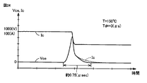
図27には、図22と同様に、第1ゲート電圧Vg1の変化タイミングから3(μs)早く、第2ゲート電圧Vg2が変化する、即ち、遅れ時間Td=−3(μs)であるときのシミュレーション波形が示される。図27では、Toffは約0.45(μs)である。 In FIG. 27, as in FIG. 22 , when the second gate voltage Vg2 changes 3 (μs) earlier than the change timing of the first gate voltage Vg1, that is, when the delay time Td = -3 (μs). The simulation waveform is shown. In FIG. 27 , Toff is about 0.45 (μs).
再び図17を参照して、図17中には、T=25℃の各シミュレーション条件(図18〜図22)でのサージ電圧Vsg、及び、T=150℃の各シミュレーション条件(図23〜図27)でのターンオフ時間Toffがさらに記入されている。 With reference to FIG. 17 again, in FIG. 17, the surge voltage Vsg under each simulation condition of T = 25 ° C. (FIGS. 18 to 22) and each simulation condition of T = 150 ° C. (FIGS. 23 to 22) are shown. The turn-off time Reference in FIG. 27) is further entered.
このようなサージ電圧の抑制効果は、nベース41に過剰に蓄積された電子が、第2のゲートチャネル領域53を通じてコレクタ電極51へ排出される電子量が調節されることによって生じている。従って、第2のゲートチャネル領域53の電気抵抗値の大小、及び、チャネル形成及び非形成の時間長さによって、過剰電子の排出速度を精緻に制御することで、サージ電圧の低減を図ることも可能である。具体的には、第2のゲートチャネル領域53の電気抵抗値の大小は、第2ゲート電圧Vg2の大きさによって制御することができ、チャネル形成及び非形成の時間長さは、第2ゲート電圧Vg2を印加する時間の長さで制御することができる。 Such an effect of suppressing the surge voltage is caused by adjusting the amount of electrons that are excessively accumulated in the n-base 41 and discharged to the collector electrode 51 through the second gate channel region 53. Thus, the magnitude of the electrical resistance of the second gate channel region 53, and, by the time length of the channel formation and non-formation, by precisely controlling the discharge speed of the excess electrons, to reduce the surge voltage Is also possible. Specifically, the magnitude of the electric resistance value of the second gate channel region 53 can be controlled by the magnitude of the second gate voltage Vg2, and the length of time for channel formation and non-formation is the second gate voltage. It can be controlled by the length of time for applying Vg2.
図29を参照して、半導体装置200のターンオフ時には、図28と同様に、第1ゲート電圧Vg1=0(V)、かつ、第2ゲート電圧Vg2=0(V)とした後で、第1ゲート電極48に対して、エミッタ電極50に対して正電圧を再び供給する期間を少なくとも1つ設けること、即ち、第1のゲートチャネル領域56でチャネルを形成するための第1ゲート電圧Vg1、及び、第2のゲートチャネル領域53でチャネルを非形成とするための第2ゲート電圧Vg2の発生を停止した後に、第1のゲートチャネル領域56でチャネルを形成するための第1ゲート電圧Vg1を発生する期間を少なくとも1つ設けることによっても、サージ電圧を軽減することができる。 With reference to FIG. 29, at the time of turn-off of the semiconductor device 200, the first gate voltage Vg1 = 0 (V) and the second gate voltage Vg2 = 0 (V) are set as in FIG. The gate electrode 48 is provided with at least one period during which the positive voltage is supplied again to the emitter electrode 50, that is, the first gate voltage Vg1 for forming a channel in the first gate channel region 56, and , After stopping the generation of the second gate voltage Vg2 for forming the channel in the second gate channel region 53, the first gate voltage Vg1 for forming the channel in the first gate channel region 56 is generated. The surge voltage can also be reduced by providing at least one period for the operation.
図30は、実施の形態1の変形例に係るゲート電圧制御の第3の例を説明するターンオン時の動作波形図である。 Figure 30 is an operating waveform diagram of turn-on explaining the third example of the gate voltage control according to a modification of the first embodiment.
実施の形態2の第1の例に係る半導体装置200aは、第1及び第2の主面を有するnベース81と、pベース82と、nエミッタ83と、pコレクタ84と、pエミッタ85と、第1トレンチ86と、第1ゲート絶縁膜87と、第1ゲート電極88と、第1ゲートの層間絶縁膜89と、エミッタ電極90と、コレクタ電極91と、nコレクタ92と、第2トレンチ100と、第2ゲート電極94と、第2ゲートの層間絶縁膜95と、第2ゲート絶縁膜97と、n型の電荷蓄積層98と、nバッファ99とを備える。 The semiconductor device 200a according to the first example of the second embodiment includes an n-base 81 having first and second main surfaces, a p-base 82, an n emitter 83, a p collector 84, and a p emitter 85. , The first trench 86, the first gate insulating film 87, the first gate electrode 88, the interlayer insulating film 89 of the first gate, the emitter electrode 90, the collector electrode 91, the n collector 92, and the second trench. It includes 100, a second gate electrode 94, an interlayer insulating film 95 of the second gate, a second gate insulating film 97, an n-type charge storage layer 98, and an n buffer 99.
第1トレンチ86は、nエミッタ83の表面からpベース82及びn型の電荷蓄積層98を貫通して、nベース81に達するように形成される。第1トレンチ86の表面には、第1ゲート絶縁膜87が形成される。第1トレンチ86の内部において、第1ゲート電極88は、第1ゲート絶縁膜87の上(第1の主面側)に形成される。半導体装置200と同様に、第1ゲート電極88は、トレンチゲート構造を有している。第1ゲート電極88は「第1の制御電極」の一実施例に対応し、第1ゲート絶縁膜87は「第1ゲート絶縁膜」の一実施例に対応する。 The first trench 86 is formed so as to penetrate the p-base 82 and the n-type charge storage layer 98 from the surface of the n-emitter 83 and reach the n-base 81. A first gate insulating film 87 is formed on the surface of the first trench 86. Inside the first trench 86, the first gate electrode 88 is formed on the first gate insulating film 87 (on the first main surface side). Similar to the semiconductor device 200, the first gate electrode 88 has a trench gate structure. The first gate electrode 88 corresponds to one embodiment of the “first control electrode”, and the first gate insulating film 87 corresponds to one embodiment of the “ first gate insulating film”.
尚、図32の半導体装置200aにおいて、nバッファ99が配置されない構造において、第2の主面側の第2ゲートを、図32と同様にトレンチゲート構造とすることも可能である。この場合には、第2トレンチ100は、nコレクタ92の表面からpコレクタ84を貫通して、nベース81に達するように形成することができる。これにより、上述した、トレンチゲート構造の採用によるターンオフ動作を高速化する効果を享受することが可能である。
In the semiconductor device 200a of FIG. 32 , in a structure in which the n-buffer 99 is not arranged, the second gate on the second main surface side may have a trench gate structure as in FIG. 32 . In this case, the
実施の形態2の第2の例に係る半導体装置200bは、第1及び第2の主面を有するnベース121と、pベース122と、nエミッタ123と、pコレクタ124と、pエミッタ125と、トレンチ126と、第1ゲート絶縁膜127と、第1ゲート電極128と、第1ゲートの層間絶縁膜129と、エミッタ電極130と、コレクタ電極131と、nコレクタ132と、第2ゲート電極134と、p型半導体領域137とを備える。 The semiconductor device 200b according to a second example of the second embodiment, the n-base 121 having first and second major surface, the p base 122, the n emitter 123, a p-type collector 124, a p-emitter 125 , Trench 126, 1st gate insulating film 127, 1st gate electrode 128, 1st gate interlayer insulating film 129, emitter electrode 130, collector electrode 131, n collector 132, and 2nd gate electrode 134. And a p-type semiconductor region 137.
第2ゲート電極134は、第2ゲートの層間絶縁膜135によってコレクタ電極131と絶縁される。nコレクタ132及びnベース121の間には、nコレクタ132及びnベース121と同一導電型(n型)の第2のゲートチャネル領域133が設けられる。p型半導体領域137は、第2ゲート電極134及びnコレクタ132の間に配設されて、第2のゲートチャネル領域133及び第2ゲート電極134を電気的に遮断する。即ち、p型半導体領域137は「第8半導体層」の一実施例に対応しており、図5での第2ゲート絶縁膜57を配設しなくても、第2のゲートチャネル領域133は、p型半導体領域137によって第2ゲート電極134から絶縁される。 The second gate electrode 134 is insulated from the collector electrode 131 by the interlayer insulating film 135 of the second gate. A second gate channel region 133 of the same conductive type (n type) as the n collector 132 and the n base 121 is provided between the n collector 132 and the n base 121. The p-type semiconductor region 137 is disposed between the second gate electrode 134 and the n collector 132 to electrically shut off the second gate channel region 133 and the second gate electrode 134 . That is, the p-type semiconductor region 137 corresponds to one embodiment of the “eighth semiconductor layer”, and the second gate channel region 133 is formed without disposing the second gate insulating film 57 in FIG. It is insulated from the second gate electrode 134 by the p-type semiconductor region 137.
nベース161は「第1の半導体層」の一実施例に対応し、半導体装置200cにおいても、n型が「第1導電型」に対応し、p型が「第2導電型に対応する。pベース162は、nベース161の第1主面に配設されており「第2の半導体層」の一実施例に対応する。nエミッタ163は、pベース162の表面に選択的に配設されており「第3の半導体層」の一実施例に対応する。高濃度のpエミッタ165は、エミッタ電極170との良好なオーミック接触を実現するために、pベース162の表面(第1の主面側)に、選択的に設けられる。pベースピラー166は、pベース162からnベース161中に深く入り込んだp型半導体領域として配設される。 The n-base 161 corresponds to an embodiment of the "first semiconductor layer", and in the semiconductor device 200c, the n-type corresponds to the "first conductive type" and the p-type corresponds to the "second conductive type". The p-base 162 is arranged on the first main surface of the n-base 161 and corresponds to one embodiment of the “second semiconductor layer”. The n-emitter 163 is selectively arranged on the surface of the p-base 162 and corresponds to one embodiment of the “third semiconductor layer”. The high-concentration p-emitter 165 is selectively provided on the surface (first main surface side) of the p-base 162 in order to realize good ohmic contact with the emitter electrode 170 . The p-base pillar 166 is arranged as a p-type semiconductor region deeply penetrated from the p-base 162 to the n-base 161.
第1の主面には、第1ゲート絶縁膜167、第1ゲート電極168、及び、第1ゲートの層間絶縁膜169によって、平面ゲート構造の第1のゲートが設けられるpベース162のうちの、nベース161及びnエミッタ163の間の領域に、第1のゲートチャネル領域176が形成される。第1のゲートチャネル領域176には、実施の形態1と同様に、エミッタ電極170を基準として第1ゲート電極168に印加される第1ゲート電圧Vg1に応じて、電流経路(チャネル)が形成又は非形成とされる。第1ゲート電圧Vg1に対する第1のゲートチャネル領域176の挙動は、実施の形態1での第1のゲートチャネル領域56の挙動と同様であるので、詳細な説明は繰り返さない。第1ゲート電極168は「第1の制御電極」の一実施例に対応し、第1ゲート絶縁膜167は「第1ゲート絶縁膜」の一実施例に対応する。 Of the p-base 162 in which the first gate of the planar gate structure is provided on the first main surface by the first gate insulating film 167, the first gate electrode 168, and the interlayer insulating film 169 of the first gate. , A first gate channel region 176 is formed in the region between the n base 161 and the n emitter 163. Similar to the first embodiment, a current path (channel) is formed in the first gate channel region 176 according to the first gate voltage Vg1 applied to the first gate electrode 168 with reference to the emitter electrode 170. It is considered non-forming. Since the behavior of the first gate channel region 176 with respect to the first gate voltage Vg1 is the same as the behavior of the first gate channel region 56 in the first embodiment, detailed description will not be repeated. The first gate electrode 168 corresponds to one embodiment of the “first control electrode”, and the first gate insulating film 167 corresponds to one embodiment of the “first gate insulating film”.
nベース161の第2の主面には、pコレクタ164が配設される。pコレクタ164は「第4の半導体層」の一実施例に対応する。高濃度のnコレクタ172は、コレクタ電極171との良好なオーミック接触を実現するために、pコレクタ164の表面(第2の主面側)に選択的に配設されており「第5の半導体層」の一実施例に対応する。コレクタ電極171は、pコレクタ164及びnコレクタ172の上(第2の主面側)に配設されて、半導体装置200cの第2の主面上に配置される。即ち、コレクタ電極171は「第2の主電極」の一実施例に対応する。 A p-collector 164 is arranged on the second main surface of the n-base 161. The p-collector 164 corresponds to an embodiment of the "fourth semiconductor layer". The high-concentration n-collector 172 is selectively arranged on the surface (second main surface side) of the p-collector 164 in order to realize good ohmic contact with the collector electrode 171. Corresponds to one embodiment of "layer". The collector electrode 171 is arranged on the p collector 164 and the n collector 172 (on the second main surface side), and is arranged on the second main surface of the semiconductor device 200c. That is, the collector electrode 171 corresponds to one embodiment of the “second main electrode”.
再び図32を参照して、半導体装置200aにおいて、pエミッタ85−pベース82−nベース81(n型の電荷蓄積層98及びnバッファ99を含む)−第2のゲートチャネル領域93(n型)−nコレクタ92の経路によって、pベース82及びnベース81のpn接合(J2接合)による寄生ダイオードが構成される。当該寄生ダイオードは、pエミッタ85がエミッタ電極90と電気的に接続され、nコレクタ92がコレクタ電極91と電気的に接続されているため、IGBTに対して逆並列に接続されて、エミッタ電極90からコレクタ電極91へ流れる逆電流(Ic<0)の経路を確保する、FWDと同様に機能する。 With reference to FIG. 32 again, in the semiconductor device 200a, the p emitter 85-p base 82-n base 81 (including the n-type charge storage layer 98 and the n-buffer 99) -the second gate channel region 93 (n-type). ) -The path of the n-collector 92 constitutes a parasitic diode with a pn junction (J2 junction) of the p-base 82 and n-base 81. Since the p emitter 85 is electrically connected to the emitter electrode 90 and the n collector 92 is electrically connected to the collector electrode 91, the parasitic diode is connected in antiparallel to the IGBT and the emitter electrode 90. It functions in the same manner as the FWD, which secures the path of the reverse current (Ic <0) flowing from the collector electrode 91 to the collector electrode 91 .
更に、逆電流通過時に、ノーマリオンの第2ゲートをオンしたまま(即ち、第2のゲートチャネル領域93はn型のまま)で、第1のゲートチャネル領域96をp型からn型に反転するように、第1ゲート電極88にエミッタ電極90に対して正電圧を印加すると(Vg1>0)、即ち、第1ゲートをオンすると、同一導電型半導体による逆電流の経路を形成することが可能である。具体的には、エミッタ電極90及びコレクタ電極91の間に、上記寄生ダイオードによる電流経路と並列に、nエミッタ83−第1のゲートチャネル領域96(n型に反転)−nベース81(n型の電荷蓄積層98及びnバッファ99を含む)−第2のゲートチャネル領域93(n型)−nコレクタ92の経路によって、逆電流を流すことができる。 Further, when the reverse current is passed, the first gate channel region 96 is inverted from p-type to n-type while the second gate of the normalion remains on (that is, the second gate channel region 93 remains n-type). When a positive voltage is applied to the emitter electrode 90 to the first gate electrode 88 (Vg1> 0), that is, when the first gate is turned on, a reverse current path by the same conductive semiconductor can be formed. It is possible. Specifically, between the emitter electrode 90 and the collector electrode 91 , in parallel with the current path by the parasitic diode, the n emitter 83-first gate channel region 96 (inverted to n type) -n base 81 (n type). (Including the charge storage layer 98 and the n-buffer 99) -second gate channel region 93 (n-type) -n collector 92 allows a reverse current to flow.
一方で、逆電流が大きい場合には、第1ゲートのオンによる電流経路の寄生抵抗によって生じる電圧降下は、pn接合を含む寄生ダイオードで生じる電圧降下よりも大きくなる。従って、逆電流の大きさに応じて、第1ゲートのオンオフを制御することで、逆電流の経路を効率的に確保することが可能となる。 On the other hand, when the reverse current is large, the voltage drop caused by the parasitic resistance of the current path due to the on of the first gate becomes larger than the voltage drop caused by the parasitic diode including the pn junction. Therefore, by controlling the on / off of the first gate according to the magnitude of the reverse current, it is possible to efficiently secure the reverse current path .
従って、電圧検出器250によって、コレクタ電極101及びエミッタ電極90の間の電圧差を測定することで、上記分流比及びIGBT内部の電気抵抗値(設計値)を用いた電流推定演算によって、逆電流Ivの等価的な検出(S110)が可能となる。尚、上述のように、第1ゲートのオンに応じて、寄生ダイオードとは異なる逆電流経路が形成されるので、上記電流推定演算で用いる電気抵抗値は、第1ゲートのオン及びオフに連動して変化させることが好ましい。 Therefore, by measuring the voltage difference between the collector electrode 101 and the emitter electrode 90 with the voltage detector 250, the reverse current is calculated by the current estimation calculation using the above-mentioned diversion ratio and the electric resistance value (design value) inside the IGBT. Equivalent detection of Iv (S 110 ) is possible. As described above, since a reverse current path different from that of the parasitic diode is formed according to the on of the first gate, the electric resistance value used in the current estimation calculation is linked to the on and off of the first gate. It is preferable to change it.
再び、図35を参照して、逆電流Ivの検出(S110)を逆バイアス電圧が小さい領域でも可能にするために、図35に従うゲート電圧制御の開始時には、第1ゲートはオンされていることが好ましい。 Again, with reference to FIG. 35, the first gate is turned on at the start of gate voltage control according to FIG. 35 to allow detection of reverse current Iv (S 110 ) even in the region where the reverse bias voltage is small. Is preferable.
駆動制御回路300は、逆電流Ivが検出されると(S110)、S120により、逆電流Ivを予め定められた電流基準値Irと比較する。逆電流Ivが電流基準値Ir以下であるとき(S120のNO判定時)には、S140により、ノーマリオフの第1ゲートをオンするように、第1ゲート電圧Vg1を制御する。一方で、ノーマリオンの第2ゲートはオンに維持される(例えば、Vg2=0)。これにより、ノーマリオンの第2ゲートを含めて、エミッタ−コレクタ間に、第1のゲートチャネル領域96及び第2のゲートチャネル領域93を経由する逆電流の経路が確保される。 When the reverse current Iv is detected (S110), the drive control circuit 300 compares the reverse current Iv with a predetermined current reference value Ir by S120. By the time the reverse current Iv is equal to or less than the current reference value Ir (determination of NO at S 120), the S140, so as to turn on the first gate of the normally-off controls the first gate voltage Vg1. On the other hand, the second gate of the normalion is kept on (eg, Vg2 = 0). As a result, a reverse current path is secured between the emitter and the collector, including the second gate of the normalization, via the first gate channel region 96 and the second gate channel region 93.
例えば、図37に示されるように、半導体装置200,200a〜200cのエミッタE及びコレクタC間に、ダイオード素子Dexを逆並列に外部接続する構成とすることで、半導体装置200,200a〜200cを高周波数でオンオフする用途に適用することが可能となる。このような外付けのダイオード素子Dexには、例えば、高速な動作が可能なSiC(炭化シリコン)−ショットキーバリアダイオード(SBD)を用いることができる。 For example, as shown in FIG. 37, the semiconductor devices 200, 200a to 200c can be connected by externally connecting the diode element Dex in antiparallel between the emitters E and collectors C of the semiconductor devices 200, 200a to 200c. It can be applied to applications that turn on and off at high frequencies. For such an external diode element Dex, for example, a SiC (silicon carbide ) -Schottky barrier diode (SBD) capable of high-speed operation can be used.
再び図32を参照して、コレクタ側の第2ゲート電極94に電圧が印加されない場合、又は、コレクタ電極91に対して正電圧が印加されて、第2ゲートがオンしている状態である。このとき、pコレクタ84−nベース81(n型の電荷蓄積層98及びnバッファ99を含む)−pベース82−nエミッタ83によって、第1ゲート電極88に印加される第1ゲート電圧Vg1に応じて、pベース82の一部にチャネルが形成される、nチャネルIGBT構造に形成される。更に、当該IGBT構造と並列に、nコレクタ92−第2のゲートチャネル領域93(n型)−nベース81(n型の電荷蓄積層98及びnバッファ99を含む)−pベース82−nエミッタ83によって、第1ゲート電極88の第1ゲート電圧Vg1に応じて、pベース82の一部にチャネルが形成されるnチャネルMOSFET構造が形成される。これらのIGBT構造及びMOSFET構造は、第1ゲート電極88を共通の制御用電極として、コレクタ−エミッタ間に並設されている。 With reference to FIG. 32 again, a voltage is not applied to the second gate electrode 94 on the collector side, or a positive voltage is applied to the collector electrode 91 and the second gate is turned on. At this time, the p collector 84-n base 81 (including the n-type charge storage layer 98 and the n buffer 99) -p base 82-n emitter 83 applies the first gate voltage Vg1 to the first gate electrode 88. Correspondingly, it is formed into an n-channel IGBT structure in which channels are formed in a part of the p-base 82. Further, in parallel with the IGBT structure, n-collector 92-second gate channel region 93 (n-type) -n-base 81 (including n-type charge storage layer 98 and n-buffer 99) -p-base 82-n emitter. by 83, in response to the first gate voltage V g1 of first gate electrode 88, n-channel MOSFET structure in which a channel is formed on a part of the p base 82 is formed. In these IGBT structures and MOSFET structures, the first gate electrode 88 is used as a common control electrode and is arranged side by side between the collector and the emitter.
一方で、IGBTは、コレクタ側のpコレクタ84及びnベース81(nバッファ99)によるpn接合であるJ1接合が順バイアスされるまでは、殆ど電流が流れない一方で、一旦電流が流れ始めると、僅かな電圧の増加に対して、電流が大幅に増加する。即ち、電圧増加量(ΔV)と電流増加量(ΔI)の比で表される微分抵抗(ΔV/ΔI)は、同一定格(同一定格電圧及び同一チップ面積)のMOSFETのオン抵抗Ronよりも、非常に小さい。通常、J1接合の順バイアスのためには、実施の形態3のダイオード動作で説明したのと同様に、0.7(V)程度が必要である。 On the other hand, in the IGBT, almost no current flows until the J1 junction, which is a pn junction by the p collector 84 and the n base 81 (n buffer 99) on the collector side, is forward biased, and once the current starts to flow. , For a slight increase in voltage, the current increases significantly. That is, the differential resistance (ΔV / ΔI) represented by the ratio of the voltage increase amount (ΔV) and the current increase amount (ΔI) is higher than the on-resistance Ron of the MOSFET having the same rating (same rated voltage and same chip area). Very small. Normally, for the forward bias of the J1 junction, about 0.7 (V) is required as described in the diode operation of the third embodiment.
この結果、実施の形態5に係るゲート電圧制御によれば、過電流検出に応じた自己保護のために半導体装置(IGBT)をターンオフする際に、過電流遮断によるdIc/dt及びサージ電圧を低減することによって、IGBTが破壊されることを防止できる。尚、実施の形態5に係るゲート電圧制御は、半導体装置200,200a〜200cに共通に適用することが可能である。 As a result, according to the gate voltage control according to the fifth embodiment, dIc / dt and surge voltage due to overcurrent interruption are reduced when the semiconductor device (IGBT) is turned off for self-protection in response to overcurrent detection. By doing so, it is possible to prevent the IGBT from being destroyed. The gate voltage control according to the fifth embodiment can be commonly applied to the semiconductor devices 200, 200a to 200c.
Claims (23)
前記第1の半導体層の前記第1の主面上に配設された第2導電型の第2の半導体層と、
前記第2の半導体層の表面に選択的に配設された前記第1導電型の第3の半導体層と、
前記第2の半導体層及び前記第3の半導体層上に配設された第1の主面側の第1の主電極と、
前記第2の半導体層のうちの、前記第1の半導体層及び前記第3の半導体層の間の領域に形成される第1のゲートチャネル領域と、
前記第1のゲートチャネル領域と第1ゲート絶縁膜によって絶縁される第1の制御電極と、
前記第1の半導体層の前記第2の主面上に配設された前記第2導電型の第4の半導体層と、
前記第4の半導体層の表面に選択的に配設された前記第1導電型の第5の半導体層と、
前記第4の半導体層及び前記第5の半導体層上に配設された第2の主面側の第2の主電極と、
前記第1の半導体層及び前記第5の半導体層の間に設けられた前記第1導電型の第2のゲートチャネル領域と、
前記第2のゲートチャネル領域と第2ゲート絶縁膜によって絶縁される第2の制御電極とを備える、半導体装置。 A first conductive type first semiconductor layer having first and second main surfaces,
A second conductive type second semiconductor layer disposed on the first main surface of the first semiconductor layer, and
The first conductive type third semiconductor layer selectively arranged on the surface of the second semiconductor layer, and the third semiconductor layer.
The first main electrode on the first main surface side disposed on the second semiconductor layer and the third semiconductor layer,
A first gate channel region formed in a region between the first semiconductor layer and the third semiconductor layer of the second semiconductor layer, and
The first gate channel region and the first control electrode insulated by the first gate insulating film,
The second conductive type fourth semiconductor layer disposed on the second main surface of the first semiconductor layer, and
The first conductive type fifth semiconductor layer selectively disposed on the surface of the fourth semiconductor layer, and the fifth semiconductor layer.
The second main electrode on the second main surface side disposed on the fourth semiconductor layer and the fifth semiconductor layer,
A second gate channel region of the first conductive type provided between the first semiconductor layer and the fifth semiconductor layer, and
A semiconductor device including the second gate channel region and a second control electrode insulated by a second gate insulating film.
前記第1のゲートチャネル領域は、前記第1の制御電極に前記第1の主電極に対して正電圧を印加することで前記第1の半導体層及び前記第3の半導体層の間にチャネルが形成されるノーマリオフ型で構成され、
前記第2のゲートチャネル領域は、前記第2の制御電極に前記第2の主電極に対して負電圧を印加することで前記第1の半導体層及び前記第5の半導体層の間のチャネルが非形成とされるノーマリオン型で構成される、請求項1記載の半導体装置。 The first conductive type is n-type, and the second conductive type is p-type.
In the first gate channel region, a channel is formed between the first semiconductor layer and the third semiconductor layer by applying a positive voltage to the first main electrode to the first control electrode. Consists of a normally-off type formed,
In the second gate channel region, a channel between the first semiconductor layer and the fifth semiconductor layer is formed by applying a negative voltage to the second main electrode to the second control electrode. The semiconductor device according to claim 1, which is composed of a non-formed normalion type.
前記第1ゲート絶縁膜は、前記第1トレンチの表面上に形成され、
前記第1の制御電極は、前記第1トレンチ内において前記第1ゲート絶縁膜の上に形成される、請求項1又は2に記載の半導体装置。 A first trench formed so as to penetrate the third semiconductor layer and the second semiconductor layer on the first main surface side and reach the first semiconductor layer is further provided.
The first gate insulating film is formed on the surface of the first trench.
The semiconductor device according to claim 1 or 2, wherein the first control electrode is formed on the first gate insulating film in the first trench.
前記第6の半導体層は、前記第1の半導体層よりも高い不純物密度で、かつ、前記第2の半導体層よりも薄く形成される、請求項1〜3のいずれか1項に記載の半導体装置。 Further comprising the first conductive type sixth semiconductor layer disposed between the first semiconductor layer and the second semiconductor layer.
The semiconductor according to any one of claims 1 to 3, wherein the sixth semiconductor layer is formed to have a higher impurity density than the first semiconductor layer and thinner than the second semiconductor layer. apparatus.
前記第7の半導体層は、前記第1の半導体層よりも高い不純物密度で、かつ、前記第4の半導体層よりも厚く形成され、
前記第2のゲートチャネル領域は、前記第7の半導体層及び前記第5の半導体層の間に設けられる、請求項1〜4のいずれか1項に記載の半導体装置。 Further comprising the first conductive type seventh semiconductor layer disposed between the first semiconductor layer and the fourth semiconductor layer.
The seventh semiconductor layer is formed to have a higher impurity density than the first semiconductor layer and thicker than the fourth semiconductor layer.
The semiconductor device according to any one of claims 1 to 4, wherein the second gate channel region is provided between the seventh semiconductor layer and the fifth semiconductor layer.
前記第2ゲート絶縁膜は、前記第2トレンチの表面上に形成され、
前記第2の制御電極は、前記第2トレンチ内において前記第2ゲート絶縁膜の上に形成される、請求項1〜4のいずれか1項に記載の半導体装置。 Further comprising a second trench formed on the second main surface side to reach the first semiconductor layer through the fifth semiconductor layer and the second gate channel region.
The second gate insulating film is formed on the surface of the second trench.
The semiconductor device according to any one of claims 1 to 4, wherein the second control electrode is formed on the second gate insulating film in the second trench.
前記第2ゲート絶縁膜は、前記第2トレンチの表面上に形成され、
前記第2の制御電極は、前記第2トレンチ内において前記第2ゲート絶縁膜の上に形成される、請求項5記載の半導体装置。 On the second main surface side, the fifth semiconductor layer and the second gate channel region are penetrated to reach the seventh semiconductor layer, but not to reach the first semiconductor layer. Further equipped with a second trench formed in
The second gate insulating film is formed on the surface of the second trench.
The semiconductor device according to claim 5, wherein the second control electrode is formed on the second gate insulating film in the second trench.
前記第2の制御電極は、前記第2ゲート絶縁膜に代えて前記第8の半導体層によって、前記第2のゲートチャネル領域と絶縁される、請求項1〜5のいずれか1項に記載の半導体装置。 Further comprising the second conductive type eighth semiconductor layer connected between the second control electrode and the second gate channel region.
The second control electrode according to any one of claims 1 to 5, wherein the second control electrode is insulated from the second gate channel region by the eighth semiconductor layer instead of the second gate insulating film. Semiconductor device.
前記第1の主電極及び前記第3の主電極間の電圧差を測定する電圧検出器とをさらに備える、請求項1〜9のいずれか1項に記載の半導体装置。 On the second main surface side, a third main electrode separated from the second main electrode and arranged on the fourth semiconductor layer and the fifth semiconductor layer,
The semiconductor device according to any one of claims 1 to 9, further comprising a voltage detector for measuring a voltage difference between the first main electrode and the third main electrode.
前記駆動制御回路は、前記第2の主電極から前記第1の主電極に電流が流れるのを遮断しているオフ動作期間において、前記電圧検出器によって検出された前記電圧差から前記第1の主電極から前記第2の主電極へ流れている逆電流を測定するとともに、当該逆電流が予め定められた基準値よりも大きい場合には、前記第1のゲートチャネル領域のチャネルを非形成とするように前記第1ゲート電圧を制御する一方で、当該逆電流が前記基準値より小さい場合に、前記第1のゲートチャネル領域のチャネルを形成するように前記第1ゲート電圧を制御する、請求項10記載の半導体装置。 A drive control circuit for controlling the first gate voltage of the first control electrode and the second gate voltage of the second control electrode is further provided.
The drive control circuit is the first from the voltage difference detected by the voltage detector during the off operation period in which the current is blocked from flowing from the second main electrode to the first main electrode. The reverse current flowing from the main electrode to the second main electrode is measured, and when the reverse current is larger than a predetermined reference value, the channel in the first gate channel region is not formed. While controlling the first gate voltage so as to form a channel in the first gate channel region when the reverse current is smaller than the reference value, the first gate voltage is controlled. Item 10. The semiconductor device according to Item 10.
前記駆動制御回路は、前記第2の主電極から前記第1の主電極に電流が流れるのを遮断している状態から、前記第2の主電極から前記第1の主電極に電流が流れる状態へ遷移する第1のスイッチング動作時において、前記第1のゲートチャネル領域にチャネルを形成するための前記第1ゲート電圧を発生するのと同時又はその直前に、前記第2のゲートチャネル領域にチャネルを非形成とするための前記第2ゲート電圧を発生する、請求項1〜10のいずれか1項に記載の半導体装置。 A drive control circuit for controlling the first gate voltage of the first control electrode and the second gate voltage of the second control electrode is further provided.
The drive control circuit is in a state in which a current flows from the second main electrode to the first main electrode from a state in which current flows from the second main electrode to the first main electrode. At the time of the first switching operation of transitioning to, the channel is connected to the second gate channel region at the same time as or immediately before the first gate voltage for forming the channel is generated in the first gate channel region. The semiconductor device according to any one of claims 1 to 10, which generates the second gate voltage for forming the non-forming.
前記駆動制御回路は、前記第2の主電極から前記第1の主電極に電流が流れている状態から、前記第2の主電極から前記第1の主電極に電流が流れるのを遮断する状態へ遷移する第2のスイッチング動作時において、前記第1のゲートチャネル領域にチャネルを形成するための前記第1ゲート電圧の発生を停止するのと同時又はその直前に、前記第2のゲートチャネル領域にチャネルを非形成とするための前記第2ゲート電圧の発生を停止する、請求項1〜10のいずれか1項に記載の半導体装置。 A drive control circuit for controlling the first gate voltage of the first control electrode and the second gate voltage of the second control electrode is further provided.
The drive control circuit is in a state of blocking the flow of current from the second main electrode to the first main electrode from the state in which a current is flowing from the second main electrode to the first main electrode. At the time of the second switching operation of transitioning to, at the same time as or immediately before stopping the generation of the first gate voltage for forming a channel in the first gate channel region, the second gate channel region The semiconductor device according to any one of claims 1 to 10, wherein the generation of the second gate voltage for forming a non-forming channel is stopped.
Priority Applications (4)
| Application Number | Priority Date | Filing Date | Title |
|---|---|---|---|
| JP2018178887A JP7068981B2 (en) | 2018-09-25 | 2018-09-25 | Semiconductor device |
| US16/507,316 US11031491B2 (en) | 2018-09-25 | 2019-07-10 | Semiconductor device |
| DE102019214213.3A DE102019214213A1 (en) | 2018-09-25 | 2019-09-18 | Semiconductor device |
| CN201910886047.5A CN110943125B (en) | 2018-09-25 | 2019-09-19 | Semiconductor device with a semiconductor device having a plurality of semiconductor chips |
Applications Claiming Priority (1)
| Application Number | Priority Date | Filing Date | Title |
|---|---|---|---|
| JP2018178887A JP7068981B2 (en) | 2018-09-25 | 2018-09-25 | Semiconductor device |
Publications (3)
| Publication Number | Publication Date |
|---|---|
| JP2020053466A JP2020053466A (en) | 2020-04-02 |
| JP2020053466A5 true JP2020053466A5 (en) | 2020-11-12 |
| JP7068981B2 JP7068981B2 (en) | 2022-05-17 |
Family
ID=69725625
Family Applications (1)
| Application Number | Title | Priority Date | Filing Date |
|---|---|---|---|
| JP2018178887A Active JP7068981B2 (en) | 2018-09-25 | 2018-09-25 | Semiconductor device |
Country Status (4)
| Country | Link |
|---|---|
| US (1) | US11031491B2 (en) |
| JP (1) | JP7068981B2 (en) |
| CN (1) | CN110943125B (en) |
| DE (1) | DE102019214213A1 (en) |
Cited By (1)
| Publication number | Priority date | Publication date | Assignee | Title |
|---|---|---|---|---|
| JP7330155B2 (en) | 2020-09-16 | 2023-08-21 | 株式会社東芝 | Semiconductor devices and semiconductor circuits |
Families Citing this family (10)
| Publication number | Priority date | Publication date | Assignee | Title |
|---|---|---|---|---|
| JP7068981B2 (en) * | 2018-09-25 | 2022-05-17 | 三菱電機株式会社 | Semiconductor device |
| JP7210342B2 (en) * | 2019-03-18 | 2023-01-23 | 株式会社東芝 | semiconductor equipment |
| JP7352443B2 (en) * | 2019-11-01 | 2023-09-28 | 株式会社東芝 | Control method for semiconductor devices |
| JP7364488B2 (en) * | 2020-02-05 | 2023-10-18 | 株式会社東芝 | semiconductor equipment |
| JP7330154B2 (en) * | 2020-09-16 | 2023-08-21 | 株式会社東芝 | Semiconductor devices and semiconductor circuits |
| JP2022073525A (en) | 2020-11-02 | 2022-05-17 | 株式会社東芝 | Semiconductor device and semiconductor module |
| JP7444027B2 (en) * | 2020-11-06 | 2024-03-06 | 三菱電機株式会社 | semiconductor equipment |
| DE102022119632A1 (en) | 2022-08-04 | 2024-02-15 | Infineon Technologies Ag | Power semiconductor device, method for producing a power semiconductor device and method for operating a power semiconductor device |
| CN116072721B (en) * | 2023-03-17 | 2023-06-30 | 深圳市威兆半导体股份有限公司 | Insulated gate bipolar transistor and carrier concentration control method thereof |
| CN116314309B (en) * | 2023-05-23 | 2023-07-25 | 四川奥库科技有限公司 | Back gate structure of reverse-conduction IGBT device and processing method thereof |
Family Cites Families (16)
| Publication number | Priority date | Publication date | Assignee | Title |
|---|---|---|---|---|
| EP0394859A1 (en) * | 1989-04-28 | 1990-10-31 | Asea Brown Boveri Ag | Bidirectional turn-off semiconductor device |
| JPH03194971A (en) * | 1989-12-22 | 1991-08-26 | Meidensha Corp | Power semiconductor element |
| JP2582724Y2 (en) * | 1991-10-08 | 1998-10-08 | 株式会社明電舎 | Insulated gate type semiconductor device |
| JP4479052B2 (en) | 2000-05-09 | 2010-06-09 | 富士電機システムズ株式会社 | Semiconductor device |
| JP5245157B2 (en) | 2008-06-03 | 2013-07-24 | 独立行政法人産業技術総合研究所 | Semiconductor bidirectional switching device |
| JP5417811B2 (en) | 2008-11-18 | 2014-02-19 | 株式会社デンソー | Semiconductor device |
| JP2010251517A (en) | 2009-04-15 | 2010-11-04 | Tokyo Electric Power Co Inc:The | Power semiconductor element |
| TWI402985B (en) * | 2009-06-02 | 2013-07-21 | Anpec Electronics Corp | Integrated structure of igbt and diode and method of forming the same |
| JP5369300B2 (en) * | 2009-09-16 | 2013-12-18 | 三菱電機株式会社 | Semiconductor device and manufacturing method thereof |
| JP5754543B2 (en) * | 2012-03-16 | 2015-07-29 | 富士電機株式会社 | Semiconductor device |
| JP5605664B2 (en) | 2013-02-25 | 2014-10-15 | 独立行政法人産業技術総合研究所 | Semiconductor bidirectional switching device |
| CN104919595B (en) * | 2013-06-24 | 2019-06-07 | 理想能量有限公司 | System, circuit with bidirectional bipolar transistor, Apparatus and method for |
| WO2015114787A1 (en) | 2014-01-31 | 2015-08-06 | 株式会社日立製作所 | Semiconductor element drive apparatus and power conversion apparatus using same |
| JP6416143B2 (en) * | 2016-03-16 | 2018-10-31 | 株式会社東芝 | Semiconductor device |
| CN107768434A (en) * | 2017-10-20 | 2018-03-06 | 电子科技大学 | A kind of two-way IGBT and its manufacture method |
| JP7068981B2 (en) * | 2018-09-25 | 2022-05-17 | 三菱電機株式会社 | Semiconductor device |
-
2018
- 2018-09-25 JP JP2018178887A patent/JP7068981B2/en active Active
-
2019
- 2019-07-10 US US16/507,316 patent/US11031491B2/en active Active
- 2019-09-18 DE DE102019214213.3A patent/DE102019214213A1/en active Pending
- 2019-09-19 CN CN201910886047.5A patent/CN110943125B/en active Active
Cited By (1)
| Publication number | Priority date | Publication date | Assignee | Title |
|---|---|---|---|---|
| JP7330155B2 (en) | 2020-09-16 | 2023-08-21 | 株式会社東芝 | Semiconductor devices and semiconductor circuits |
Similar Documents
| Publication | Publication Date | Title |
|---|---|---|
| JP2020053466A5 (en) | ||
| JP7068981B2 (en) | Semiconductor device | |
| JP6407455B2 (en) | Semiconductor device | |
| JP7379327B2 (en) | semiconductor device | |
| US9087809B2 (en) | Ultra-fast breakover diode | |
| JP5513112B2 (en) | Avalanche protection for wide band gap devices | |
| JPWO2011111500A1 (en) | Semiconductor device | |
| JPH04291767A (en) | Conductivity modulation mosfet | |
| JPH11345969A (en) | Power semiconductor device | |
| US10304970B2 (en) | Packaged overvoltage protection circuit for triggering thyristors | |
| US20150187678A1 (en) | Power semiconductor device | |
| JP2002532885A (en) | Output semiconductor circuit | |
| US9741835B2 (en) | Semiconductor device and insulated gate bipolar transistor with transistor cells and sensor cell | |
| US9231092B2 (en) | Bi-directional switch with Q1 and Q4 control | |
| US20150187922A1 (en) | Power semiconductor device | |
| KR101994728B1 (en) | Power semiconductor device | |
| US20150187869A1 (en) | Power semiconductor device | |
| EP0862220A1 (en) | Semiconductor switching device and a power converter using the same and a drive method therefor | |
| US20150187919A1 (en) | Power semiconductor device | |
| RU91222U1 (en) | POWERFUL FIELD CONTROLLED FIELD CONTROLLER | |
| Iwamuro et al. | A new concept for high voltage MCCT with no J-FET resistance by using a very thin wafer | |
| Vobecky et al. | Cathode emitter versus carrier lifetime engineering of thyristors for industrial applications | |
| JPS6145865B2 (en) | ||
| Lutz et al. | Thyristors | |
| CN113661576A (en) | Semiconductor device with a plurality of semiconductor chips |