次に、本発明の一実施形態であるプリント配線板が図面を参照しながら説明される。図1には、一実施形態のプリント配線板の一例であるプリント配線板1の断面図が示されている。図1に示されるように、プリント配線板1は、第1面10Fおよび第1面10Fと反対側の第2面10Sを備える下基板10を備えている。下基板10の第1面10Fは、下基板10の積層方向の一方に露出する最上層11の面からなる。また、下基板10の第2面10Sは、下基板10の積層方向の他方に露出する最下層12と最下層12の開口部から露出する中間層13の一部の面からなる。プリント配線板1はさらに、下基板10の第1面10F側に積層される上基板5を備えている。
Next, a printed wiring board according to an embodiment of the present invention will be described with reference to the drawings. FIG. 1 is a cross-sectional view of a printed wiring board 1 which is an example of a printed wiring board according to one embodiment. As shown in FIG. 1, the printed wiring board 1 includes a lower substrate 10 having a first surface 10F and a second surface 10S opposite to the first surface 10F. The first surface 10F of the lower substrate 10 includes the surface of the uppermost layer 11 that is exposed on one side in the stacking direction of the lower substrate 10. The second surface 10S of the lower substrate 10 includes the lowermost layer 12 exposed to the other side in the stacking direction of the lower substrate 10 and a part of the surface of the intermediate layer 13 exposed from the opening of the lowermost layer 12. The printed wiring board 1 further includes an upper substrate 5 laminated on the first surface 10F side of the lower substrate 10.
最上層11は第1面10F側に第1導体層110を有しており、第1導体層110は少なくとも1つの部品実装パッド115を含んでいる。そして、プリント配線板1は、上基板5を貫通して、部品実装パッド115の一面115sを含む下基板10の第1面10Fの一部を露出するキャビティ7を備えている。キャビティ7には、プリント配線板1に実装される、半導体装置などの外部の電子部品(図示せず)が収容される。部品実装パッド115には、このような外部の電子部品の端子が、はんだなどの接合材を介して、または直接、接続される。
The uppermost layer 11 has a first conductive layer 110 on the first surface 10F side, and the first conductive layer 110 includes at least one component mounting pad 115. The printed wiring board 1 includes a cavity 7 that penetrates through the upper substrate 5 and exposes a part of the first surface 10F of the lower substrate 10 including one surface 115s of the component mounting pad 115. The cavity 7 accommodates an external electronic component (not shown) such as a semiconductor device mounted on the printed wiring board 1. Terminals of such external electronic components are connected to the component mounting pads 115 via a bonding material such as solder or directly.
図1に示される例では、下基板10は、第1面10Fを構成する最上層11と、第2面10Sを構成する最下層12、および最上層11と最下層12の間に形成される中間層13と、第2中間層14を有している。最上層11は絶縁層101と第1導体層110、および絶縁層110の第1導体層101と反対側に形成される第2導体層111を有している。最下層12は絶縁層である。中間層13は絶縁層103と、絶縁層103に接して形成される導体層130を有し、第2中間層14は絶縁層104と、絶縁層104に接して形成される導体層140を有している。図1の例では、下基板10には絶縁層および導体層がそれぞれ4層形成されているが、絶縁層および導体層がさらに積層されて4層よりも多く形成されてよい。たとえば、第2中間層14を構成する絶縁層104および導体層140が複数形成されてよい。下基板10がより多くの導体層を含むことにより、プリント配線板1の平面サイズを大きくすることなく、より規模が大きく複雑な電気回路をプリント配線板1内に形成することが可能となる。絶縁層および導体層がさらに追加して形成された例は図2を参照して後述される。
In the example shown in FIG. 1, the lower substrate 10 is formed on the uppermost layer 11 constituting the first surface 10F, the lowermost layer 12 constituting the second surface 10S, and between the uppermost layer 11 and the lowermost layer 12. It has an intermediate layer 13 and a second intermediate layer 14. The uppermost layer 11 has an insulating layer 101 and a first conductive layer 110, and a second conductive layer 111 formed on the insulating layer 110 on the side opposite to the first conductive layer 101. The lowermost layer 12 is an insulating layer. The intermediate layer 13 has an insulating layer 103 and a conductor layer 130 formed in contact with the insulating layer 103, and the second intermediate layer 14 has an insulating layer 104 and a conductor layer 140 formed in contact with the insulating layer 104. are doing. In the example of FIG. 1, the lower substrate 10 has four insulating layers and four conductor layers, respectively. However, the insulating layer and the conductor layers may be further laminated to form more than four layers. For example, a plurality of insulating layers 104 and conductor layers 140 constituting second intermediate layer 14 may be formed. Since the lower substrate 10 includes more conductor layers, a larger and more complicated electric circuit can be formed in the printed wiring board 1 without increasing the planar size of the printed wiring board 1. An example in which an insulating layer and a conductor layer are additionally formed will be described later with reference to FIG.
下基板10の第2面10Sの一部を構成する中間層13が有する導体層130は、下側接続パッド135を含んでいる。下側接続パッド135は、たとえば、プリント配線板1が用いられる電子機器のマザーボードや、積層構造を有する半導体装置のパッケージ基板などとの接続に用いられ得る。
The conductor layer 130 included in the intermediate layer 13 that constitutes a part of the second surface 10S of the lower substrate 10 includes the lower connection pad 135. The lower connection pad 135 can be used, for example, for connection to a motherboard of an electronic device using the printed wiring board 1 or a package substrate of a semiconductor device having a laminated structure.
下基板10に含まれる絶縁層は任意の絶縁性樹脂を用いて形成される。下基板10の最上層11、最下層12、および中間層13は互いに異なる材料を含む絶縁層を有している。最上層11の絶縁層101は第1の材料を含み、最下層12は第2の材料を含み、中間層13の絶縁層103は第3の材料を含んでいる。第2中間層14の絶縁層104は第4の材料を含んでおり、第4の材料は第1の材料と同じであり得る。図1に示される例では、下基板10の絶縁層101および絶縁層104に含まれる第1の材料と第4の材料は、芯材を含有する樹脂であり、第2および第3の材料は芯材を含有しない樹脂である。
The insulating layer included in the lower substrate 10 is formed using an arbitrary insulating resin. The uppermost layer 11, the lowermost layer 12, and the intermediate layer 13 of the lower substrate 10 have insulating layers containing different materials. The insulating layer 101 of the uppermost layer 11 contains the first material, the lowermost layer 12 contains the second material, and the insulating layer 103 of the intermediate layer 13 contains the third material. The insulating layer 104 of the second intermediate layer 14 includes a fourth material, which may be the same as the first material. In the example shown in FIG. 1, the first material and the fourth material included in the insulating layer 101 and the insulating layer 104 of the lower substrate 10 are a resin containing a core material, and the second and third materials are It is a resin that does not contain a core material.
最上層11の絶縁層101に含まれる第1の材料は、たとえばガラス繊維やアラミド繊維などの芯材、および芯材に含浸されたエポキシ樹脂などの絶縁性樹脂が例示される。第2中間層14の絶縁層104に含まれる第4の材料も第1の材料と同様に芯材に含浸された樹脂である。中間層13の絶縁層103に含まれる第3の材料は芯材を含んでいない任意の絶縁性樹脂であり、たとえばエポキシ樹脂である。そして最下層12に含まれる第2の材料は芯材を含んでおらず、たとえば、感光性のポリイミド樹脂やエポキシ樹脂である。第1、第2、第3、および第4の材料はシリカなどの無機フィラーを含み得る。
Examples of the first material included in the insulating layer 101 of the uppermost layer 11 include a core material such as glass fiber and aramid fiber, and an insulating resin such as an epoxy resin impregnated in the core material. The fourth material included in the insulating layer 104 of the second intermediate layer 14 is also a resin impregnated in a core material, like the first material. The third material included in the insulating layer 103 of the intermediate layer 13 is any insulating resin that does not include a core material, for example, an epoxy resin. The second material contained in the lowermost layer 12 does not include a core material, and is, for example, a photosensitive polyimide resin or an epoxy resin. The first, second, third, and fourth materials may include an inorganic filler such as silica.
図1に示される例では、下基板10の第1面10F側に積層される上基板5は、下基板10に対して反対側の最表に形成される上層52と、上層52と下基板10の間に形成される下層53と、下層53と下基板10の間に形成される追加層54とを有している。上層52は絶縁層である。下層53は絶縁層503と、絶縁層503に接して形成される導体層530を有している。追加層54は絶縁層504と、絶縁層504に接して形成される導体層540を有している。絶縁層504は下基板10の絶縁層104と同じく第4の材料を含んでいる。絶縁層503は下基板10の絶縁層103と同じく第3の材料を含んでいる。上層52は、下基板10の最下層12と同じく第2の材料を含んでいる。導体層530は、電子部品や外部の配線板(図示せず)との接続に用いられ得る上側接続パッド535を含んでいる。上側接続パッド535に接続されるこれらの配線板や電子部品は、たとえば、キャビティ7を跨ぐように、導体層530上に配置され得る。
In the example shown in FIG. 1, the upper substrate 5 laminated on the first surface 10F side of the lower substrate 10 includes an upper layer 52 formed on the outermost surface on the opposite side to the lower substrate 10, an upper layer 52 and the lower substrate 10, and an additional layer 54 formed between the lower layer 53 and the lower substrate 10. The upper layer 52 is an insulating layer. The lower layer 53 includes an insulating layer 503 and a conductor layer 530 formed in contact with the insulating layer 503. The additional layer 54 has an insulating layer 504 and a conductor layer 540 formed in contact with the insulating layer 504. The insulating layer 504 contains the fourth material, similarly to the insulating layer 104 of the lower substrate 10. The insulating layer 503 contains the third material, similarly to the insulating layer 103 of the lower substrate 10. The upper layer 52 contains the second material, like the lowermost layer 12 of the lower substrate 10. The conductor layer 530 includes an upper connection pad 535 that can be used for connection to an electronic component or an external wiring board (not shown). These wiring boards and electronic components connected to the upper connection pads 535 can be arranged on the conductor layer 530 so as to straddle the cavity 7, for example.
絶縁層101、第1導体層110、および第2導体層111から構成される最上層11はコア基板100として形成されてよい。すなわち、プリント配線板1の製造過程においては、後述されるように、コア基板100を出発基板として、第2導体層111が形成されている側に第2中間層14、中間層13、最下層12が順次積層され、下基板10が形成される。また、コア基板100の第1導体層110が形成されている側には、追加層54、下層53、上層52が一般的なビルドアップ配線板の製造方法により順次積層されて上基板5が形成される。図1に示される例では、コア基板100を中心にして、第1導体層110側と第2導体層111側で対称な層構造が形成されている。絶縁層101と第1導体層110および第2導体層111からなるコア基板100は両面銅張積層板を加工して形成され得る。
The uppermost layer 11 including the insulating layer 101, the first conductor layer 110, and the second conductor layer 111 may be formed as the core substrate 100. That is, in the manufacturing process of the printed wiring board 1, as described later, the second intermediate layer 14, the intermediate layer 13, and the lowermost layer are provided on the side where the second conductor layer 111 is formed, using the core substrate 100 as a starting substrate. 12 are sequentially laminated to form the lower substrate 10. On the side of the core substrate 100 where the first conductor layer 110 is formed, the additional layer 54, the lower layer 53, and the upper layer 52 are sequentially laminated by a general build-up wiring board manufacturing method to form the upper substrate 5. Is done. In the example shown in FIG. 1, a symmetric layer structure is formed on the first conductor layer 110 side and the second conductor layer 111 side around the core substrate 100. The core substrate 100 including the insulating layer 101, the first conductor layer 110, and the second conductor layer 111 can be formed by processing a double-sided copper-clad laminate.
下基板10の絶縁層103に含まれる第3の材料は、絶縁層101に含まれる第1の材料よりも熱膨張率が高い。たとえば第1の材料の熱膨張率は約5〜7ppm/℃であり、第3の材料の熱膨張率は約20ppm/℃である。プリント配線板1に上層52と最下層12が形成されておらず、キャビティ7が形成されていない状態(図4E参照)を考えると、低温度から高温度への温度変化が生じた場合に、最上層11と第2中間層14および中間層13とで構成される積層体には、絶縁層101と絶縁層103の熱膨張率の違いに起因する、U字に反る(絶縁層101側が凹になり絶縁層103側が凸になる)応力が発生する。一方、最上層11の第2中間層14と反対の側には、最上層11に対して第2中間層14および中間層13と対称になるように、追加層54と下層53が配されており、下層53の絶縁層503は絶縁層103と同じく第3の材料を含んでいる。このため、絶縁層101と絶縁層503の熱膨張率の違いにより、上述の絶縁層101と絶縁層103の間で発生する応力とは反対方向の応力が発生し、全体としての反りは生じにくくなっている。しかし、上層52と最下層12が形成されていない状態の積層体(図4E参照)にキャビティが形成された状態を仮定すると、キャビティが形成された領域においては、絶縁層101と絶縁層103の間で発生する応力が打ち消されずに上述のU字状の反りが生じ得る。
The third material included in the insulating layer 103 of the lower substrate 10 has a higher coefficient of thermal expansion than the first material included in the insulating layer 101. For example, the first material has a coefficient of thermal expansion of about 5-7 ppm / ° C, and the third material has a coefficient of thermal expansion of about 20 ppm / ° C. Considering a state where the upper layer 52 and the lowermost layer 12 are not formed on the printed wiring board 1 and the cavity 7 is not formed (see FIG. 4E), when a temperature change from a low temperature to a high temperature occurs, The laminate composed of the uppermost layer 11, the second intermediate layer 14, and the intermediate layer 13 has a U-shape (the insulating layer 101 side has a warp due to a difference in thermal expansion coefficient between the insulating layer 101 and the insulating layer 103). (The recess becomes concave and the insulating layer 103 becomes convex.) A stress is generated. On the other hand, on the side of the uppermost layer 11 opposite to the second intermediate layer 14, an additional layer 54 and a lower layer 53 are arranged so as to be symmetrical with respect to the uppermost layer 11 with respect to the second intermediate layer 14 and the intermediate layer 13. The insulating layer 503 of the lower layer 53 contains the third material as in the case of the insulating layer 103. For this reason, due to the difference in the coefficient of thermal expansion between the insulating layer 101 and the insulating layer 503, a stress in a direction opposite to the stress generated between the insulating layer 101 and the insulating layer 103 described above is generated, and warpage as a whole hardly occurs. Has become. However, assuming a state in which a cavity is formed in the stacked body in which the upper layer 52 and the lowermost layer 12 are not formed (see FIG. 4E), in the region where the cavity is formed, the insulating layer 101 and the insulating layer 103 are not formed. The above-mentioned U-shaped warpage may occur without canceling out the stress generated between them.
本実施形態では、第3の材料よりも熱膨張率の低い第2の材料を含む最下層12が中間層13の最上層11と反対側に接して形成されている。たとえば、最下層12に含まれる第2の材料の熱膨張率は約10ppm/℃である。プリント配線板1では、熱膨張率が第3の材料よりも低い第2の材料を含む最下層12が、中間層13の最上層11と反対側に配されることにより、キャビティ7が形成されている領域においても下基板10の反りが抑制され得る。反りを効果的に抑制する観点から第2の材料の熱膨張率は第1の材料の熱膨張率よりも高く第1の材料の熱膨張率と第2の材料の熱膨張率との差は、第3の材料の熱膨張率と第2の材料の熱膨張率との差よりも小さいことが好ましい。第1の材料と第2の材料の熱膨張率がより近いことで、生じる反りの程度を小さくし得る。なお、第4の材料としては、熱膨張率が第3の材料よりも低いものが使用され、第1の材料と同じであってもよい。
In the present embodiment, the lowermost layer 12 containing the second material having a lower coefficient of thermal expansion than the third material is formed in contact with the intermediate layer 13 on the side opposite to the uppermost layer 11. For example, the second material contained in the lowermost layer 12 has a coefficient of thermal expansion of about 10 ppm / ° C. In the printed wiring board 1, the cavity 7 is formed by disposing the lowermost layer 12 including the second material having a lower coefficient of thermal expansion than the third material on the side opposite to the uppermost layer 11 of the intermediate layer 13. The warp of the lower substrate 10 can be suppressed even in the region where the lower substrate 10 is located. From the viewpoint of effectively suppressing warpage, the thermal expansion coefficient of the second material is higher than the thermal expansion coefficient of the first material, and the difference between the thermal expansion coefficient of the first material and the thermal expansion coefficient of the second material is Preferably, the difference between the coefficient of thermal expansion of the third material and the coefficient of thermal expansion of the second material is smaller. The closer the first material and the second material have a coefficient of thermal expansion, the smaller the degree of warpage that can occur. As the fourth material, a material having a lower coefficient of thermal expansion than the third material is used, and may be the same as the first material.
図1の例では最下層12はソルダーレジスト層として形成されている。ソルダーレジスト層である最下層12は、たとえば、感光性のポリイミド樹脂やエポキシ樹脂を用いて形成され、下側接続パッド135を露出させる開口135aを有している。プリント配線板1の反りが抑制されると同時に、下側接続パッド135上に供されるはんだなどの接合材の濡れ広がりが抑制される。近接する下側接続パッド135同士のショート不良が抑制されながら、良好な品質で電子機器のマザーボードや、積層構造を有する半導体装置のパッケージ基板などと接続され得る。
In the example of FIG. 1, the lowermost layer 12 is formed as a solder resist layer. The lowermost layer 12, which is a solder resist layer, is formed using, for example, a photosensitive polyimide resin or an epoxy resin, and has an opening 135a for exposing the lower connection pad 135. The warpage of the printed wiring board 1 is suppressed, and at the same time, the spread of a bonding material such as solder provided on the lower connection pad 135 is suppressed. It can be connected to a motherboard of an electronic device, a package substrate of a semiconductor device having a laminated structure, or the like with good quality while suppressing short circuit failure between adjacent lower connection pads 135.
上基板5の上層52もソルダーレジスト層として形成されている。ソルダーレジスト層である上層52は、下基板10のソルダーレジスト層である最下層12と同じく、たとえば、感光性のポリイミド樹脂やエポキシ樹脂を用いて形成されている。上層52は、上側接続パッド535を露出させる開口535aを有している。
The upper layer 52 of the upper substrate 5 is also formed as a solder resist layer. The upper layer 52, which is a solder resist layer, is formed using, for example, a photosensitive polyimide resin or an epoxy resin, similarly to the lowermost layer 12, which is a solder resist layer of the lower substrate 10. The upper layer 52 has an opening 535a exposing the upper connection pad 535.
図示されていないが、部品実装パッド115、下側接続パッド135、ならびに上側接続パッド535の露出面には、保護膜が形成されていてもよい。このような保護膜は、たとえば、Ni/Au、Ni/Pd/Au、またはSnなどの複数または単一の金属めっき膜であってよく、また、OSP膜であってもよい。なお、キャビティ7の開口形状やプリント配線板1内での形成位置、ならびに、部品実装パッド115や上側および下側の各接続パッド535、135の配列パターンは、図1に示される例に限定されない。
Although not shown, a protective film may be formed on the exposed surfaces of the component mounting pad 115, the lower connection pad 135, and the upper connection pad 535. Such a protective film may be, for example, a plurality or a single metal plating film of Ni / Au, Ni / Pd / Au, Sn, or the like, or may be an OSP film. In addition, the opening shape of the cavity 7, the formation position in the printed wiring board 1, and the arrangement pattern of the component mounting pads 115 and the upper and lower connection pads 535, 135 are not limited to the example shown in FIG. .
プリント配線板1に含まれる導体層530、540、140、130、第1導体層110、および第2導体層111は、銅やニッケルなどの、適切な導電性を備えている任意の材料を用いて形成され得る。好ましくは、銅箔、電解銅めっき膜、もしくは無電解銅めっき膜、またはこれらの組み合わせによって形成されている。導体層540、導体層140、第1導体層110、および第2導体層111は3層構造を有しており、それぞれ金属箔層112、金属膜層113、電解めっき膜層114、を有している(図1において、符号112〜114は、第1導体層110だけに付され、第2導体層111、導体層130、140、530、および540に対するこれらの符号は省略されている)。そして、導体層130および導体層530は2層構造を有しており、金属膜層と電解めっき膜層を有している。しかし、各導体層の構成は、図1に例示される層構造に限定される訳ではない。
The conductor layers 530, 540, 140, and 130, the first conductor layer 110, and the second conductor layer 111 included in the printed wiring board 1 are made of any material having appropriate conductivity, such as copper or nickel. Can be formed. Preferably, it is formed of a copper foil, an electrolytic copper plating film, an electroless copper plating film, or a combination thereof. The conductor layer 540, the conductor layer 140, the first conductor layer 110, and the second conductor layer 111 have a three-layer structure, and include a metal foil layer 112, a metal film layer 113, and an electrolytic plating film layer 114, respectively. (In FIG. 1, reference numerals 112 to 114 are assigned only to the first conductor layer 110, and these reference numerals for the second conductor layer 111, the conductor layers 130, 140, 530, and 540 are omitted.) The conductor layer 130 and the conductor layer 530 have a two-layer structure, and have a metal film layer and an electrolytic plating film layer. However, the configuration of each conductor layer is not limited to the layer structure illustrated in FIG.
上基板5には、上基板5を構成している導体層を接続するビア導体が形成されている。図1の例では、絶縁層503を貫通して導体層530と導体層540とを接続するビア導体531と、絶縁層504を貫通して導体層540と第1導体層110とを接続するビア導体541が形成されている。ビア導体531およびビア導体541は、第1導体層110に向って縮径するテーパー形状を有している。なお、便宜上、「縮径」という文言が用いられているが、ビア導体531、541および後述の他の各ビア導体の開口形状は、必ずしも円形に限定されない。「縮径」は、単にビア導体の水平断面における外周上の最長の2点間の距離が小さくなることを意味している。
Via conductors are formed on the upper substrate 5 to connect the conductor layers constituting the upper substrate 5. In the example of FIG. 1, a via conductor 531 penetrating the insulating layer 503 to connect the conductor layer 530 and the conductor layer 540, and a via conductor penetrating the insulating layer 504 to connect the conductor layer 540 to the first conductor layer 110 A conductor 541 is formed. The via conductor 531 and the via conductor 541 have a tapered shape whose diameter decreases toward the first conductor layer 110. Although the term “diameter reduction” is used for convenience, the opening shapes of the via conductors 531 and 541 and other via conductors to be described later are not necessarily limited to circular shapes. “Reduced diameter” simply means that the distance between the two longest points on the outer circumference in the horizontal cross section of the via conductor is reduced.
下基板10内の中間層13には、絶縁層103を貫通して導体層130と導体層140とを接続するビア導体131が形成されている。第2中間層14には、絶縁層104を貫通して導体層140と第2導体層111とを接続するビア導体141が形成されている。ビア導体131、141は、第2導体層111に向って縮径しており、上基板5内のビア導体531、541が縮径する方向と逆方向に縮径するテーパー形状を有している。ビア導体531、541、131、および141は、好ましくは、無電解銅めっき膜と電解銅めっき膜とで形成される。ビア導体531、541、131、および141は、それぞれ、導体層530、540、130、および導体層140を構成している金属膜層および電解めっき膜層と一体的に形成され得る。
In the intermediate layer 13 in the lower substrate 10, a via conductor 131 that penetrates through the insulating layer 103 and connects the conductor layer 130 and the conductor layer 140 is formed. In the second intermediate layer 14, a via conductor 141 that penetrates through the insulating layer 104 and connects the conductor layer 140 and the second conductor layer 111 is formed. The via conductors 131 and 141 have a diameter reduced toward the second conductor layer 111 and have a tapered shape in which the diameter of the via conductors 531 and 541 in the upper substrate 5 is reduced in a direction opposite to the diameter reduced. . Via conductors 531, 541, 131, and 141 are preferably formed of an electroless copper plating film and an electrolytic copper plating film. The via conductors 531, 541, 131, and 141 can be formed integrally with the metal film layer and the electrolytic plating film layer constituting the conductor layers 530, 540, 130, and the conductor layer 140, respectively.
最上層11の絶縁層101にはスルーホール導体116が形成されている。スルーホール導体116は、絶縁層101を貫通して第1導体層110および第2導体層111を互いに接続している。スルーホール導体116は、絶縁層101の厚さ方向の中央部を境に第1導体層110側および第2導体層111側それぞれにおいて、絶縁層101の厚さ方向の中央部に向って縮径するテーパー形状を有している。
In the insulating layer 101 of the uppermost layer 11, a through-hole conductor 116 is formed. The through-hole conductor 116 penetrates the insulating layer 101 and connects the first conductor layer 110 and the second conductor layer 111 to each other. The diameter of the through-hole conductor 116 is reduced toward the center in the thickness direction of the insulating layer 101 on each of the first conductor layer 110 side and the second conductor layer 111 side from the center in the thickness direction of the insulating layer 101. It has a tapered shape.
本実施形態では、プリント配線板1の上基板5および下基板10の層構造は、図1に示されるプリント配線板1の例と異なってもよい。上基板5の下層53および追加層54、ならびに、下基板10の中間層13および第2中間層14は、複数の絶縁層と導体層から構成されてもよい。より複雑な電気回路がプリント配線板1の中に形成され得る。下層53、追加層54、中間層13、第2中間層14が複数の絶縁層と導体層で構成された例は、本実施形態の他の例であるプリント配線板1aとして、図2を参照して次に説明される。
In the present embodiment, the layer structure of the upper substrate 5 and the lower substrate 10 of the printed wiring board 1 may be different from the example of the printed wiring board 1 shown in FIG. The lower layer 53 and the additional layer 54 of the upper substrate 5, and the intermediate layer 13 and the second intermediate layer 14 of the lower substrate 10 may be composed of a plurality of insulating layers and conductor layers. More complicated electric circuits can be formed in the printed wiring board 1. An example in which the lower layer 53, the additional layer 54, the intermediate layer 13, and the second intermediate layer 14 are composed of a plurality of insulating layers and conductor layers is shown in FIG. 2 as a printed wiring board 1a as another example of the present embodiment. And will be explained next.
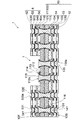
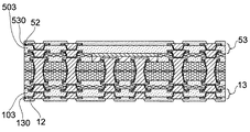
図2には、本実施形態の他の例であるプリント配線板1aの層構造が模式的に示されている。プリント配線板1aでは、上基板5の下層53は、それぞれ複数の絶縁層503と導体層530から構成されており、追加層54はそれぞれ複数の絶縁層504と導体層540から構成されている。また、下基板10の中間層13は、それぞれ複数の絶縁層103と導体層130から構成されており、第2中間層14は複数の絶縁層104と導体層140から構成されている。図2の模式図では、絶縁層と導体層による層構造と、各層を貫通して形成されるビア導体およびスルーホール導体が模式的に示され、プリント配線板1aの他の構成要素である、接続パッド、導体層内の金属箔、金属膜などの構成要素の表示は省略され、またその説明も省略される。
FIG. 2 schematically shows a layer structure of a printed wiring board 1a which is another example of the present embodiment. In the printed wiring board 1a, the lower layer 53 of the upper substrate 5 includes a plurality of insulating layers 503 and a conductor layer 530, and the additional layer 54 includes a plurality of insulating layers 504 and a conductor layer 540, respectively. The intermediate layer 13 of the lower substrate 10 includes a plurality of insulating layers 103 and conductor layers 130, and the second intermediate layer 14 includes a plurality of insulating layers 104 and conductor layers 140. In the schematic diagram of FIG. 2, a layer structure including an insulating layer and a conductor layer, a via conductor and a through-hole conductor formed through each layer are schematically illustrated, and are other components of the printed wiring board 1a. The display of components such as connection pads, metal foils and metal films in the conductor layer is omitted, and the description thereof is also omitted.
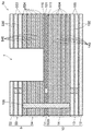
図2に示される例では、プリント配線板1aは上基板5および下基板10を含み、中央部にキャビティ7が形成されている。下基板10では、中間層13を構成する絶縁層103が2層形成され、2層の絶縁層103の各々に接して導体層130が形成されている。そして第2中間層14を構成する絶縁層104は5層形成され、5層の絶縁層104の各々に接して導体層140が形成されている。
In the example shown in FIG. 2, the printed wiring board 1a includes an upper substrate 5 and a lower substrate 10, and a cavity 7 is formed at the center. On the lower substrate 10, two insulating layers 103 constituting the intermediate layer 13 are formed, and a conductor layer 130 is formed in contact with each of the two insulating layers 103. Then, five insulating layers 104 constituting the second intermediate layer 14 are formed, and a conductor layer 140 is formed in contact with each of the five insulating layers 104.
上基板5では、下層53を構成する絶縁層503が2層形成されており、2層の絶縁層503の各々に接して導体層530が形成されている。そして、追加層54を構成する絶縁層504は5層形成され、5層の絶縁層504の各々に接して導体層540が形成されている。なお、図2に示される例では、絶縁層103と絶縁層503は2層形成され、絶縁層104と絶縁層504は5層形成されているが、形成される層数はこれに限定されない。
On the upper substrate 5, two insulating layers 503 constituting the lower layer 53 are formed, and a conductor layer 530 is formed in contact with each of the two insulating layers 503. Then, five insulating layers 504 constituting the additional layer 54 are formed, and a conductor layer 540 is formed in contact with each of the five insulating layers 504. Note that in the example illustrated in FIG. 2, the insulating layer 103 and the insulating layer 503 are formed in two layers, and the insulating layer 104 and the insulating layer 504 are formed in five layers; however, the number of layers formed is not limited to this.
プリント配線板1aでは、各絶縁層に含まれる材料はプリント配線板1と同様である。最上層11(コア基板100)の絶縁層101は第1の材料を含み、絶縁層103は第3の材料を含み、絶縁層104は第4の材料を含み、第4の材料は第1の材料と同じであり得る。絶縁層503は第3の材料を含み、絶縁層504は第4の材料を含む。下基板10の最下層12、および上基板5の上層52は、図1に示されるプリント配線板1と同じく、ソルダーレジスト層として形成されてよい。プリント配線板1と同様に、プリント配線板1aにおいても、第3の材料の熱膨張率は第1の材料および第2の材料の熱膨張率よりも高い。第3の材料よりも熱膨張率の低い第2の材料を含む最下層12が配されることで、下基板10の絶縁層の熱膨張率の違いによる反りが抑制され得る。追加された絶縁層には、必要に応じて適宜、プリント配線板1a内の各導体層を接続するビア導体が形成され得る。なお、プリント配線板1aには図2に模式的に示されるように、追加層54、コア基板100、および第2中間層14を貫通して導体層540と導体層140を接続するスルーホール導体166が形成されてもよい。
In the printed wiring board 1a, the material contained in each insulating layer is the same as that of the printed wiring board 1. The insulating layer 101 of the uppermost layer 11 (core substrate 100) includes a first material, the insulating layer 103 includes a third material, the insulating layer 104 includes a fourth material, and the fourth material includes a first material. It can be the same as the material. The insulating layer 503 includes a third material, and the insulating layer 504 includes a fourth material. The lowermost layer 12 of the lower substrate 10 and the upper layer 52 of the upper substrate 5 may be formed as solder resist layers, similarly to the printed wiring board 1 shown in FIG. Similarly to the printed wiring board 1, also in the printed wiring board 1a, the thermal expansion coefficient of the third material is higher than the thermal expansion coefficients of the first material and the second material. By arranging the lowermost layer 12 including the second material having a lower coefficient of thermal expansion than the third material, warpage due to a difference in the coefficient of thermal expansion of the insulating layer of the lower substrate 10 can be suppressed. Via conductors for connecting the respective conductor layers in the printed wiring board 1a may be formed on the added insulating layer as needed. As shown schematically in FIG. 2, the printed wiring board 1a has a through-hole conductor that connects the conductor layer 540 and the conductor layer 140 through the additional layer 54, the core substrate 100, and the second intermediate layer 14. 166 may be formed.
次に、一実施形態のプリント配線板のさらに他の例が図面を参照して説明される。図3には、他の実施形態のプリント配線板の一例であるプリント配線板1bの断面図が示されている。プリント配線板1bにおける下基板10は、第1面10Fおよび第2面10Sを備えている。下基板10は、絶縁層101、第1導体層110、および第2導体層111から構成される最上層11と、絶縁層103、導体層130から構成される中間層13と、最下層12とで構成されている。プリント配線板1bの下基板10はプリント配線板1、1aの例とは異なり、第2中間層14は設けられていない。また、最上層11はプリント配線板1bのコア基板としては形成されていない。プリント配線板1、1aは、下基板および上基板の形成はコア基板100(図1参照)を出発基板として、その両面に絶縁層および導体層が順次積層されることで形成され得るが、後述されるように、プリント配線板1bは異なる方法により形成される。
Next, still another example of the printed wiring board of one embodiment will be described with reference to the drawings. FIG. 3 is a cross-sectional view of a printed wiring board 1b which is an example of a printed wiring board according to another embodiment. The lower substrate 10 in the printed wiring board 1b has a first surface 10F and a second surface 10S. The lower substrate 10 includes an uppermost layer 11 including an insulating layer 101, a first conductive layer 110, and a second conductive layer 111; an intermediate layer 13 including an insulating layer 103 and a conductive layer 130; It is composed of Unlike the printed wiring boards 1 and 1a, the lower substrate 10 of the printed wiring board 1b is not provided with the second intermediate layer 14. Further, the uppermost layer 11 is not formed as a core substrate of the printed wiring board 1b. The printed wiring boards 1 and 1a can be formed by sequentially laminating an insulating layer and a conductor layer on both sides of a lower substrate and an upper substrate, starting from a core substrate 100 (see FIG. 1). As described above, the printed wiring board 1b is formed by a different method.
下基板10内の各絶縁層(図3の例では絶縁層101、103、および最下層12)は、エポキシ樹脂などの任意の絶縁性樹脂を用いて形成され、プリント配線板1と同様に、絶縁層101は第1の材料を、最下層12は第2の材料を、絶縁層103は第3の材料を含んでいる。第1、第2、および第3の材料の熱膨張率の関係はプリント配線板1と同じく、第3の材料が第1の材料および第2の材料よりも高い。第1の材料と第3の材料の熱膨張率の差に起因する下基板10の反りは、ソルダーレジスト層として形成される最下層12が配されることによって抑制され得る。好ましくは、第2の材料の熱膨張率が第1の材料の熱膨張率よりも高く、第1の材料の熱膨張率と第2の材料の熱膨張率との差が、第3の材料と第2の材料の熱膨張率の差よりも小さい。絶縁層の熱膨張率の差に起因する基板の反りの程度が効果的に抑制され得る。図1に示されるプリント配線板1の例と同様に、絶縁層101は芯材を含んでいる。芯材としては、たとえば、ガラス繊維やアラミド繊維などが例示される。そして、下基板10の絶縁層101以外の絶縁層、すなわち、絶縁層101より第2面10S側に位置する全ての絶縁層(図3の例では絶縁層103および最下層12)は芯材を含まない。
Each insulating layer (the insulating layers 101 and 103 and the lowermost layer 12 in the example of FIG. 3) in the lower substrate 10 is formed using an arbitrary insulating resin such as an epoxy resin. The insulating layer 101 contains the first material, the lowermost layer 12 contains the second material, and the insulating layer 103 contains the third material. The relationship between the coefficients of thermal expansion of the first, second, and third materials is higher in the third material than in the first material and the second material, as in the printed wiring board 1. The warpage of the lower substrate 10 due to the difference in the coefficient of thermal expansion between the first material and the third material can be suppressed by disposing the lowermost layer 12 formed as a solder resist layer. Preferably, the coefficient of thermal expansion of the second material is higher than the coefficient of thermal expansion of the first material, and the difference between the coefficient of thermal expansion of the first material and the coefficient of thermal expansion of the second material is the third material. Is smaller than the difference between the thermal expansion coefficients of the first and second materials. The degree of warpage of the substrate due to the difference in the coefficient of thermal expansion of the insulating layer can be effectively suppressed. As in the example of the printed wiring board 1 shown in FIG. 1, the insulating layer 101 includes a core material. Examples of the core material include glass fiber and aramid fiber. An insulating layer other than the insulating layer 101 of the lower substrate 10, that is, all insulating layers (the insulating layer 103 and the lowermost layer 12 in the example of FIG. 3) located on the second surface 10S side of the insulating layer 101 have a core material. Not included.
図3に示されるプリント配線板1bでは上基板5は、上層52と、上層52と下基板10との間に配される絶縁層503と導体層530からなる下層53とで構成されている。プリント配線板1bの上基板5は、プリント配線板1、1aの例と異なり、追加層54は設けられておらず、また、下層53を構成する絶縁層503は2層設けられている。上層52はプリント配線板1と同様に、第2の材料を含むソルダーレジスト層として設けられている。絶縁層503は第4の材料を含み、たとえば、絶縁層101に含まれる第1の材料と同じ材料で形成され、ガラス繊維などの芯材にエポキシ樹脂などの樹脂材料を含浸してなるプリプレグで形成されてよい。絶縁層503が絶縁層101と同じく芯材を含むことで、キャビティ7の剛性は向上し得る。
In the printed wiring board 1b shown in FIG. 3, the upper substrate 5 includes an upper layer 52, an insulating layer 503 disposed between the upper layer 52 and the lower substrate 10, and a lower layer 53 including a conductor layer 530. The upper substrate 5 of the printed wiring board 1b is different from the examples of the printed wiring boards 1 and 1a in that no additional layer 54 is provided, and two insulating layers 503 constituting the lower layer 53 are provided. The upper layer 52 is provided as a solder resist layer containing the second material, similarly to the printed wiring board 1. The insulating layer 503 includes a fourth material. For example, the insulating layer 503 is formed of the same material as the first material included in the insulating layer 101, and is made of a prepreg obtained by impregnating a core material such as glass fiber with a resin material such as an epoxy resin. May be formed. When the insulating layer 503 includes the core material as in the case of the insulating layer 101, the rigidity of the cavity 7 can be improved.
プリント配線板1bが有する導体層は、図1のプリント配線板1と同様に、銅やニッケルなどの適切な導電性を備えている任意の材料を用いて形成され得る。好ましくは銅箔、電解銅めっき膜、もしくは無電解銅めっき膜、またはこれらの組み合わせで形成されている。第1導体層110は一層で形成され、好ましくは電解めっき膜により形成される。第1導体層110は、絶縁層101内に埋め込まれ、キャビティ7の底面において部品実装パッドの一面115sを下基板10の第1面10F側に、絶縁層101の一面101sより凹んだ位置に露出している。キャビティ7の底面に露出する部品実装パッド115上に供されるはんだなどの接合材の濡れ広がりが抑制される。第2導体層111、および導体層530は3層構造を有し、図1のプリント配線板1と同様に、金属箔層、金属膜層、および電解めっき膜層を有している。導体層130は2層構造を有し、金属膜層、電解めっき膜層を有している。プリント配線板1bでは、プリント配線板1のスルーホール導体116に代えて第1導体層110と第2導体層111を接続し、第1導体層110へ向って縮径するビア導体117が形成されている。絶縁層103には、第2導体層111と導体層130を接続して第2導体層111側に向って縮径するビア導体131が形成されている。そして、上基板5には、2層の絶縁層503を貫通して導体層530と下基板10の第1導体層110とを接続するビア導体536が形成されている。
The conductive layer included in the printed wiring board 1b can be formed using any material having appropriate conductivity, such as copper or nickel, similarly to the printed wiring board 1 in FIG. Preferably, it is formed of a copper foil, an electrolytic copper plating film, an electroless copper plating film, or a combination thereof. The first conductor layer 110 is formed of a single layer, and is preferably formed of an electrolytic plating film. The first conductor layer 110 is embedded in the insulating layer 101 and exposes one surface 115 s of the component mounting pad on the bottom surface of the cavity 7 toward the first surface 10 F of the lower substrate 10 at a position recessed from the one surface 101 s of the insulating layer 101. are doing. Wetting and spreading of a bonding material such as solder provided on the component mounting pad 115 exposed on the bottom surface of the cavity 7 is suppressed. The second conductor layer 111 and the conductor layer 530 have a three-layer structure, and have a metal foil layer, a metal film layer, and an electrolytic plating film layer, similarly to the printed wiring board 1 of FIG. The conductor layer 130 has a two-layer structure, and has a metal film layer and an electrolytic plating film layer. In the printed wiring board 1 b, a via conductor 117 is formed instead of the through-hole conductor 116 of the printed wiring board 1, connecting the first conductor layer 110 and the second conductor layer 111 and reducing the diameter toward the first conductor layer 110. ing. In the insulating layer 103, a via conductor 131 that connects the second conductor layer 111 and the conductor layer 130 and decreases in diameter toward the second conductor layer 111 is formed. The upper substrate 5 has a via conductor 536 that penetrates through the two insulating layers 503 and connects the conductor layer 530 to the first conductor layer 110 of the lower substrate 10.
次に、図1に示されるプリント配線板1を例にして、一実施形態のプリント配線板の製造方法が図4A〜4Hを参照して以下に説明される。まず、図4Aに示される、芯材を含む絶縁層101と、絶縁層101の両面に、たとえば熱圧着などにより積層されている銅箔122からなる銅張積層板99が準備される。絶縁層101は第1の材料を含み、第1の材料はガラス繊維やアラミド繊維などの芯材にエポキシ樹脂などの絶縁性樹脂を含浸させたものである。
Next, taking the printed wiring board 1 shown in FIG. 1 as an example, a method of manufacturing a printed wiring board according to one embodiment will be described below with reference to FIGS. First, as shown in FIG. 4A, a copper-clad laminate 99 made of an insulating layer 101 including a core material and a copper foil 122 laminated on both surfaces of the insulating layer 101 by, for example, thermocompression bonding is prepared. The insulating layer 101 includes a first material, and the first material is obtained by impregnating a core material such as glass fiber or aramid fiber with an insulating resin such as an epoxy resin.
次いで、図4Bに示されるように、絶縁層101のスルーホール導体116の形成箇所に、炭酸ガスレーザーなどの照射によって導通用孔116aが形成される。そしてサブトラクティブ法やセミアディティブ法を用いて所望の導体パターンを有する第1導体層110および第2導体層111が形成される。同時に導通用孔116a内にスルーホール導体116が、第1および第2導体層110、111と一体的に形成される。プリント配線板1の出発基板となるコア基板100が完成する。
Next, as shown in FIG. 4B, a conduction hole 116a is formed in the insulating layer 101 at a position where the through-hole conductor 116 is formed by irradiation with a carbon dioxide gas laser or the like. Then, the first conductor layer 110 and the second conductor layer 111 having a desired conductor pattern are formed by using a subtractive method or a semi-additive method. At the same time, a through-hole conductor 116 is formed integrally with the first and second conductor layers 110 and 111 in the conduction hole 116a. A core substrate 100 serving as a starting substrate of the printed wiring board 1 is completed.
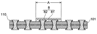
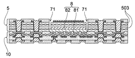
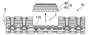
図4Cに示されるように、キャビティ7の開口形状に基づく平面形状を有する剥離膜8が絶縁層101および第1導体層110上に設けられる。剥離膜8は粘着層81と接合層82を有している。剥離膜8は粘着層81側を第1導体層110に向けて設けられる。粘着層81は、第1導体層110と絶縁層101とは強固に接着せず、しかしこれらと密着し得る材料で形成される。粘着層81には、たとえばアクリル樹脂が用いられる。一方、接合層82は剥離膜8上に配される上基板5(図1参照)を構成する絶縁層に対して十分な接着性を発現し得る材料で形成される。接合層82にはたとえばポリイミド樹脂が用いられる。剥離膜8はコア基板100の第1導体層110側のキャビティ7が形成される領域(形成領域A)に形成される。剥離膜8はキャビティ7の形成領域Aの全領域に及ぶように設けられる。また、剥離膜8は、たとえば粘着層81だけの一層で構成されてもよく、粘着層81と接合層82との間に中間層を含む3層構造を有していてもよい。たとえば、中間層の厚さを調節することによって剥離膜8の厚さが所望の厚さに調整されてもよい。
As shown in FIG. 4C, a release film 8 having a planar shape based on the opening shape of the cavity 7 is provided on the insulating layer 101 and the first conductor layer 110. The release film 8 has an adhesive layer 81 and a bonding layer 82. The release film 8 is provided with the adhesive layer 81 side facing the first conductor layer 110. The adhesive layer 81 is formed of a material that does not strongly adhere to the first conductor layer 110 and the insulating layer 101, but can adhere to them. For the adhesive layer 81, for example, an acrylic resin is used. On the other hand, the bonding layer 82 is formed of a material that can exhibit sufficient adhesiveness to the insulating layer constituting the upper substrate 5 (see FIG. 1) disposed on the release film 8. For example, a polyimide resin is used for the bonding layer 82. The release film 8 is formed in a region (formation region A) of the core substrate 100 where the cavity 7 is formed on the first conductor layer 110 side. The release film 8 is provided so as to cover the entire region A where the cavity 7 is formed. Further, the release film 8 may be composed of, for example, only one layer of the adhesive layer 81, or may have a three-layer structure including an intermediate layer between the adhesive layer 81 and the bonding layer 82. For example, the thickness of the release film 8 may be adjusted to a desired thickness by adjusting the thickness of the intermediate layer.
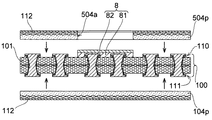
図4Dに示されるように、コア基板100の第2導体層111側に絶縁層104となるプリプレグ104pが積層され、第1導体層110側には絶縁層504となるプリプレグ504pが積層される。このプリプレグが硬化することによって絶縁層104、504が形成される。つぎのステップで形成される導体層140および導体層540の一部を構成する金属箔層112もプリプレグ上に積層される。さらに図4Eに示されるように、絶縁層104に接して導体層140が形成されることで第2中間層14が形成され、絶縁層504に接して導体層540が形成されることで追加層54が形成される。さらに、第2中間層14に接して絶縁層103と導体層130が積層されることで中間層13が形成され、追加層54に接して絶縁層503と導体層530が積層されることで下層53が形成される。一般的なビルドアップ配線板の製造方法が用いられ得る。
As shown in FIG. 4D, a prepreg 104p serving as the insulating layer 104 is stacked on the second conductor layer 111 side of the core substrate 100, and a prepreg 504p serving as the insulating layer 504 is stacked on the first conductor layer 110 side. The insulating layers 104 and 504 are formed by curing the prepreg. The conductor layer 140 and the metal foil layer 112 constituting a part of the conductor layer 540 formed in the next step are also laminated on the prepreg. 4E, the second intermediate layer 14 is formed by forming the conductor layer 140 in contact with the insulating layer 104, and the additional layer is formed by forming the conductor layer 540 in contact with the insulating layer 504. 54 are formed. Further, the intermediate layer 13 is formed by laminating the insulating layer 103 and the conductor layer 130 in contact with the second intermediate layer 14, and the lower layer is formed by laminating the insulating layer 503 and the conductor layer 530 in contact with the additional layer 54. 53 are formed. A general build-up wiring board manufacturing method can be used.
絶縁層101および第2導体層111に接して積層される第4の材料を含む絶縁層104は、たとえばエポキシ樹脂などを含浸させた芯材を有するプリプレグである。絶縁層101および第1導体層110に接して積層される絶縁層504も絶縁層104と同じく第4の材料を含む。絶縁層504は、剥離膜8の平面形状に基づく開口504aを有する。絶縁層504は、開口504aの内部に剥離膜8が収まるように、開口504aと剥離膜8を対向させて積層される。第3の材料を含む絶縁層103は、第2中間層14の導体層140が形成されている側へ、フィルム状のエポキシ樹脂などの熱圧着によって積層される。絶縁層503は、絶縁層103と同様に第3の材料を含んでおり、追加層54の導体層540が形成されている側に積層される。
The insulating layer 104 including the fourth material laminated in contact with the insulating layer 101 and the second conductor layer 111 is, for example, a prepreg having a core material impregnated with an epoxy resin or the like. The insulating layer 504 stacked in contact with the insulating layer 101 and the first conductor layer 110 also includes the fourth material, like the insulating layer 104. The insulating layer 504 has an opening 504 a based on the planar shape of the release film 8. The insulating layer 504 is stacked with the opening 504a and the release film 8 facing each other such that the release film 8 fits inside the opening 504a. The insulating layer 103 containing the third material is laminated on the side of the second intermediate layer 14 where the conductor layer 140 is formed by thermocompression bonding of a film-like epoxy resin or the like. The insulating layer 503 includes the third material similarly to the insulating layer 103, and is stacked on the side of the additional layer 54 where the conductor layer 540 is formed.
次いで、図4Fに示されるように、中間層13の絶縁層103および導体層130に接して、最下層12がソルダーレジスト層として形成される。また、下層53の絶縁層503および導体層530に接してソルダーレジスト層として上層52が形成される。ソルダーレジスト層である最下層12および上層52は、第2の材料を含んでおり、たとえば感光性エポキシ樹脂などの塗布ならびに露光および現像によって形成される。
Next, as shown in FIG. 4F, the lowermost layer 12 is formed as a solder resist layer in contact with insulating layer 103 and conductive layer 130 of intermediate layer 13. Also, the upper layer 52 is formed as a solder resist layer in contact with the insulating layer 503 and the conductor layer 530 of the lower layer 53. The lowermost layer 12 and the upper layer 52, which are solder resist layers, include a second material, and are formed by, for example, applying a photosensitive epoxy resin or the like, and exposing and developing.
図4Gに示されるように、剥離膜8の周縁に沿って、上基板5の上層52および下層53を貫通する溝71が、上基板5の下基板10と反対側の表面側から形成される。溝71は剥離膜8の周囲全周にわたってキャビティ7の形成領域Aを囲むように形成される。図4Gの例では、ソルダーレジスト層である上層52の側からレーザー光Bが照射される。レーザー光Bの種類としては、炭酸ガスレーザー、YAGレーザーなどが例示されるが、レーザー光Bはこれらに限定されない。また、溝71は、ドリル加工などの切削加工によって形成されてもよい。
As shown in FIG. 4G, a groove 71 penetrating the upper layer 52 and the lower layer 53 of the upper substrate 5 is formed along the periphery of the release film 8 from the surface side opposite to the lower substrate 10 of the upper substrate 5. . The groove 71 is formed so as to surround the formation region A of the cavity 7 over the entire periphery of the separation film 8. In the example of FIG. 4G, laser light B is irradiated from the side of the upper layer 52 which is a solder resist layer. Examples of the type of the laser beam B include a carbon dioxide gas laser and a YAG laser, but the laser beam B is not limited thereto. Further, the groove 71 may be formed by cutting such as drilling.
次いで、溝71に囲まれた上基板5の一部が剥離膜8と共に除去される。この結果、図4Hに示されるように、部品実装パッド115を底面に露出するキャビティ7が形成される。剥離膜8の粘着層81は、下基板10と強固に接着せずに単にその粘着性によって付着しているだけである。従って、除去は任意の方法で容易に行われ得る。たとえば、除去される上基板5の表面が治工具などに吸着され、下基板10と反対側に引き上げられることにより除去され得る。以上の工程を経ることによって、図1に示される本実施形態の一例であるプリント配線板1が完成する。
Next, a part of the upper substrate 5 surrounded by the groove 71 is removed together with the release film 8. As a result, as shown in FIG. 4H, a cavity 7 exposing the component mounting pad 115 on the bottom surface is formed. The adhesive layer 81 of the release film 8 does not strongly adhere to the lower substrate 10 but merely adheres by its adhesiveness. Thus, removal can be easily performed in any manner. For example, the surface of the upper substrate 5 to be removed is sucked by a jig or the like, and can be removed by being pulled up to the side opposite to the lower substrate 10. Through the above steps, the printed wiring board 1 as an example of the present embodiment shown in FIG. 1 is completed.
図2に示されるプリント配線板1aが製造される場合には、プリント配線板1の製造方法における、コア基板100の第2導体層111側への第2中間層14の形成工程が繰り返されることで、第2中間層14として複数の絶縁層104と導体層140が形成される。第2中間層14が形成された後、プリント配線板1の製造方法における中間層13の形成工程が繰り返され、第2中間層14のコア基板100と反対の側に複数の絶縁層103および導体層130を有する中間層13が形成される。複数の絶縁層104および絶縁層103には、必要に応じでビア導体が形成される。
When the printed wiring board 1a shown in FIG. 2 is manufactured, the step of forming the second intermediate layer 14 on the second conductor layer 111 side of the core substrate 100 in the method of manufacturing the printed wiring board 1 is repeated. Thus, a plurality of insulating layers 104 and a conductor layer 140 are formed as the second intermediate layer 14. After the second intermediate layer 14 is formed, the step of forming the intermediate layer 13 in the method of manufacturing the printed wiring board 1 is repeated, and a plurality of insulating layers 103 and conductors are formed on the second intermediate layer 14 on the side opposite to the core substrate 100. An intermediate layer 13 having a layer 130 is formed. Via conductors are formed in the plurality of insulating layers 104 and 103 as needed.
コア基板100の第1導体層110側においても、絶縁層504と導体層540の積層が繰り返され、追加層54として複数の絶縁層504と導体層540が形成される。なお、追加層54における複数の絶縁層504のうち、コア基板100に接して形成される絶縁層504のみが、上述のプリント配線板1の製造方法における絶縁層504と同じく開口504aを有し、この開口504aが剥離膜8と対向して積層される。そして、下層53の形成工程が繰り返されることにより、追加層54のコア基板100と反対の側に、複数の絶縁層503と導体層530を有する下層53が形成される。
Also on the first conductor layer 110 side of the core substrate 100, the lamination of the insulation layer 504 and the conductor layer 540 is repeated, and the plurality of insulation layers 504 and the conductor layer 540 are formed as the additional layer 54. Note that, among the plurality of insulating layers 504 in the additional layer 54, only the insulating layer 504 formed in contact with the core substrate 100 has an opening 504a, like the insulating layer 504 in the above-described method for manufacturing the printed wiring board 1, The opening 504a is stacked facing the release film 8. Then, by repeating the process of forming the lower layer 53, the lower layer 53 having the plurality of insulating layers 503 and the conductor layer 530 is formed on the side of the additional layer 54 opposite to the core substrate 100.
プリント配線板1aのように第2中間層14および追加層54が複数の絶縁層および導体層から構成される場合には、コア基板100と追加層54および第2中間層14とは、積層プレスによって一体的に同時に形成されてもよい。たとえば、コア基板100が準備され、コア基板100の第1導体層110側に、たとえば両面に所望のパターンに形成された導体層540を有する絶縁層504がプリプレグを介して必要な数だけ重ねられる。コア基板100の導体層111側には、たとえば両面に所望のパターンに形成された導体層140を有する絶縁層104がプリプレグを介して必要な数だけ重ねられる。そして重ねられた構成を一組として加圧加熱することでプリプレグを硬化させ、コア基板100と第2中間層14および追加層54が一体的に形成された積層体が得られる。積層体の形成の後に、図2に示されるように、追加層54、コア基板100、および第2中間層14を貫通するスルーホール導体166が形成されてもよい。
When the second intermediate layer 14 and the additional layer 54 are composed of a plurality of insulating layers and conductor layers as in the printed wiring board 1a, the core substrate 100 and the additional layer 54 and the second intermediate layer 14 May be integrally formed at the same time. For example, a core substrate 100 is prepared, and a required number of insulating layers 504 having, for example, conductor layers 540 formed in a desired pattern on both surfaces are laminated on the first conductor layer 110 side of the core substrate 100 via a prepreg. . On the conductor layer 111 side of the core substrate 100, for example, a required number of insulating layers 104 each having a conductor layer 140 formed in a desired pattern on both surfaces are stacked via a prepreg. Then, the prepreg is cured by applying pressure and heating to the stacked configuration as a set, and a laminate in which the core substrate 100, the second intermediate layer 14, and the additional layer 54 are integrally formed is obtained. After the formation of the stacked body, as shown in FIG. 2, a through-hole conductor 166 penetrating through the additional layer 54, the core substrate 100, and the second intermediate layer 14 may be formed.
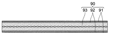
次に、他の実施形態であるプリント配線板1bの製造方法が図5A〜5Hを参照して説明される。まず、図5Aに示されるように、コア材93およびその表面に金属箔91を有するベース板90が用意される。コア材93には、たとえばガラスエポキシ基板が用いられる。金属箔91は一面に接着されたキャリア金属箔92を備えており、キャリア金属箔92とコア材93とが熱圧着などにより接合されている。
Next, a method for manufacturing a printed wiring board 1b according to another embodiment will be described with reference to FIGS. First, as shown in FIG. 5A, a base material 90 having a core material 93 and a metal foil 91 on its surface is prepared. As the core material 93, for example, a glass epoxy substrate is used. The metal foil 91 has a carrier metal foil 92 adhered to one surface, and the carrier metal foil 92 and the core material 93 are joined by thermocompression bonding or the like.
図5Bに示されるように、ベース板90上に第1導体層110が形成される。たとえば、図示されないめっきレジストが金属箔91上に形成され、めっきレジストの開口部に、金属箔91をシード層とする電解めっきにより電解銅めっき膜が形成される。その後、めっきレジストが除去され、所望の導体パターンを含む第1導体層110が形成される。第1導体層110は、無電解めっきなどで形成されてもよい。
As shown in FIG. 5B, the first conductor layer 110 is formed on the base plate 90. For example, a plating resist (not shown) is formed on metal foil 91, and an electrolytic copper plating film is formed in the opening of the plating resist by electrolytic plating using metal foil 91 as a seed layer. Thereafter, the plating resist is removed, and a first conductor layer 110 including a desired conductor pattern is formed. The first conductor layer 110 may be formed by electroless plating or the like.
次いで、図5Cに示されるように、ベース板90上および第1導体層110上に絶縁層および導体層が積層され、下基板10が形成される。まず、ガラス繊維やアラミド繊維などの芯材、および芯材に含浸されたエポキシ樹脂などの絶縁性樹脂などによって構成されるプリプレグが、第1導体層110およびベース板90の露出部分上に積層され、その硬化物として第1の材料を含む絶縁層101が形成される。つぎのステップで形成される第2導体層111の一部を構成する金属箔もプリプレグ上に積層される。なお、図5Cではベース板90の両側(上側と下側)に下基板10が形成されている状態が示されているが、符号はベース板90の下側の各要素にのみに付され、これをもとに説明される。
Next, as shown in FIG. 5C, the insulating layer and the conductor layer are laminated on the base plate 90 and the first conductor layer 110, and the lower substrate 10 is formed. First, a prepreg composed of a core material such as glass fiber or aramid fiber, and an insulating resin such as an epoxy resin impregnated in the core material is laminated on the exposed portions of the first conductor layer 110 and the base plate 90. Then, an insulating layer 101 containing the first material is formed as a cured product thereof. The metal foil constituting a part of the second conductor layer 111 formed in the next step is also laminated on the prepreg. Although FIG. 5C shows a state in which the lower substrate 10 is formed on both sides (upper and lower sides) of the base plate 90, reference numerals are given only to the respective elements on the lower side of the base plate 90. It is explained based on this.
その後、ビア導体117の形成場所に対応する位置の絶縁層101に、たとえばCO2レーザー光の照射によって導通用孔が形成される。そして、導通用孔内および絶縁層101の上に積層された金属箔の表面上に、無電解銅めっきなどによって金属膜が形成される。さらに、この金属膜をシード層として用いて、パターンめっき法を用いて銅などからなる電解めっき膜が形成される。その後、パターンめっきに用いられたレジストが除去され、その除去により露出する金属膜(および金属箔)が除去される。その結果、所望の導体パターンを含む第2導体層111が形成される。また、導通用孔内にビア導体117が形成される。下基板10の最上層11が完成する。
After that, a conduction hole is formed in the insulating layer 101 at a position corresponding to the formation location of the via conductor 117 by, for example, irradiation of a CO 2 laser beam. Then, a metal film is formed by electroless copper plating or the like on the surface of the metal foil laminated on the conduction hole and on the insulating layer 101. Further, using this metal film as a seed layer, an electrolytic plating film made of copper or the like is formed by a pattern plating method. Thereafter, the resist used for pattern plating is removed, and the metal film (and metal foil) exposed by the removal is removed. As a result, a second conductor layer 111 including a desired conductor pattern is formed. Also, a via conductor 117 is formed in the conduction hole. The uppermost layer 11 of the lower substrate 10 is completed.
中間層13は、最上層11の絶縁層101および第2導体層111へ、第3の材料を含む絶縁層103となるフィルム状のエポキシ樹脂などの熱圧着と導体層130の積層によって形成される。次いで、ソルダーレジスト層として第2の材料を含む最下層12が、導体層130および絶縁層103の表面上への感光性のエポキシ樹脂やポリイミド樹脂からなる樹脂層の形成によって形成される。そして、フォトリソグラフィ技術により、下側接続パッド135を露出させる開口135aが形成される。その結果、下基板10がベース板90上に形成される。
The intermediate layer 13 is formed on the insulating layer 101 and the second conductive layer 111 of the uppermost layer 11 by thermocompression bonding of a film-like epoxy resin or the like that becomes the insulating layer 103 containing the third material and lamination of the conductive layer 130. . Next, the lowermost layer 12 containing the second material as a solder resist layer is formed by forming a resin layer made of a photosensitive epoxy resin or a polyimide resin on the surfaces of the conductor layer 130 and the insulating layer 103. Then, an opening 135a exposing the lower connection pad 135 is formed by photolithography. As a result, the lower substrate 10 is formed on the base plate 90.
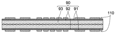
その後、ベース板90が除去され、図5Dに示されるように、第1導体層110および絶縁層101が露出する側(下基板10の第1面10F側)のキャビティ7の形成領域Aに、粘着層81と接合層82を有する剥離膜8が設けられる。ベース板90の除去により露出する第1導体層110の一面110sは、エッチングされることによって絶縁層101の露出面101sよりも凹んでいる。
After that, the base plate 90 is removed, and as shown in FIG. 5D, the first conductor layer 110 and the insulating layer 101 are exposed to the exposed region (the first surface 10F side of the lower substrate 10) in the formation region A of the cavity 7; A release film 8 having an adhesive layer 81 and a bonding layer 82 is provided. One surface 110s of the first conductor layer 110 exposed by removing the base plate 90 is recessed from the exposed surface 101s of the insulating layer 101 by being etched.
続いて、図5Eに示されるように、ガラス繊維やアラミド繊維などの芯材、および、芯材に含浸されたエポキシ樹脂などの絶縁性樹脂によって主に構成され、剥離膜8の平面形状に基づく開口を有するプリプレグ503p1が用意される。プリプレグ503p1は下基板10の第1面10Fに接して積層される。さらに、下基板10の平面形状と略同じ形状のプリプレグ503p2が用意される。プリプレグ503p2はプリプレグ503p1と同様の樹脂材料で構成され同様の芯材を含む。プリプレグ503p2の表面上には、銅などからなる金属箔層112が積層される。そして、プリプレグ503p2の金属箔層112側とは反対側がプリプレグ503p1と対向するように、プリプレグ503p2が、プリプレグ503p1上に積層される。プリプレグ503p1、503p2の硬化物として図3に示される上基板5の下層53を構成する2層の絶縁層503が形成される。
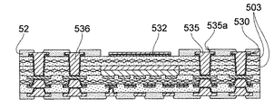
Subsequently, as shown in FIG. 5E, it is mainly formed of a core material such as glass fiber or aramid fiber, and an insulating resin such as an epoxy resin impregnated in the core material, and is based on the planar shape of the release film 8. A prepreg 503p1 having an opening is prepared. The prepreg 503p1 is stacked in contact with the first surface 10F of the lower substrate 10. Further, a prepreg 503p2 having substantially the same shape as the planar shape of the lower substrate 10 is prepared. The prepreg 503p2 is made of the same resin material as the prepreg 503p1, and includes the same core material. The metal foil layer 112 made of copper or the like is laminated on the surface of the prepreg 503p2. The prepreg 503p2 is laminated on the prepreg 503p1 such that the side of the prepreg 503p2 opposite to the metal foil layer 112 side faces the prepreg 503p1. Two insulating layers 503 constituting the lower layer 53 of the upper substrate 5 shown in FIG. 3 are formed as cured products of the prepregs 503p1 and 503p2.
次いで、図5Fに示されるように、絶縁層503上に導体層530が形成されると共に、ビア導体536が形成される。導体層530およびビア導体536は、上述の第2導体層111およびビア導体117と同様の方法で形成される。なお、図5Fに示されている例では、導体層530は、キャビティ7(図5H参照)の形成領域内に導体パターン532を含んでいる。製造途中のプリント配線板における反りの抑制に有利な場合がある。次いで、ソルダーレジスト層として第2の材料を含む上層52が形成される。導体層530および絶縁層503の表面上への感光性のエポキシ樹脂やポリイミド樹脂層の形成によって、上層52が形成される。そして、フォトリソグラフィ技術を用いて、上側接続パッド535を露出する開口535aが形成される。
Next, as shown in FIG. 5F, a conductor layer 530 is formed on the insulating layer 503, and a via conductor 536 is formed. Conductive layer 530 and via conductor 536 are formed in the same manner as second conductive layer 111 and via conductor 117 described above. In the example shown in FIG. 5F, the conductor layer 530 includes the conductor pattern 532 in the region where the cavity 7 (see FIG. 5H) is formed. In some cases, it is advantageous to suppress warpage in a printed wiring board during manufacturing. Next, an upper layer 52 containing a second material is formed as a solder resist layer. The upper layer 52 is formed by forming a photosensitive epoxy resin or polyimide resin layer on the surfaces of the conductor layer 530 and the insulating layer 503. Then, an opening 535a exposing the upper connection pad 535 is formed by using a photolithography technique.
次に、図5Gに示されるように、剥離膜8の周縁に沿って絶縁層503を貫通する溝71が上基板5の下基板10とは反対側の表面側から形成される。次いで、溝71に囲まれた上基板5の一部が剥離膜8と共に除去される。この結果、図5Hに示されるように、部品実装パッド115を底面に露出するキャビティ7が形成される。溝71の形成、および溝71に囲まれた上基板5の一部の除去は、プリント配線板1の製造方法における溝71の形成および上基板5の一部の除去と同様の方法で行われ得る。溝71の形成はドリル加工などの切削加工によって形成されてもよい。キャビティ7を有するプリント配線板1bが完成する。
Next, as shown in FIG. 5G, a groove 71 penetrating the insulating layer 503 along the periphery of the peeling film 8 is formed from the surface side of the upper substrate 5 opposite to the lower substrate 10. Next, a part of the upper substrate 5 surrounded by the groove 71 is removed together with the release film 8. As a result, as shown in FIG. 5H, the cavity 7 exposing the component mounting pad 115 on the bottom surface is formed. The formation of the groove 71 and the removal of a part of the upper substrate 5 surrounded by the groove 71 are performed in the same manner as the formation of the groove 71 and the removal of a part of the upper substrate 5 in the method of manufacturing the printed wiring board 1. obtain. The groove 71 may be formed by cutting such as drilling. The printed wiring board 1b having the cavity 7 is completed.
実施形態のプリント配線板は、各図面に例示される構造や、本明細書において例示された構造や材料を備えるものに限定されない。また、プリント配線板の製造方法は、各図面を参照して説明された方法に限定されず、その条件や順序などは適宜変更されてよい。現に製造されるプリント配線板の構造に応じて、一部の工程が省略されてもよく、別の工程が追加されてもよい。
The printed wiring board according to the embodiment is not limited to the structure illustrated in each drawing or the one including the structure or material illustrated in this specification. Further, the method of manufacturing the printed wiring board is not limited to the method described with reference to each drawing, and the conditions and order may be appropriately changed. Some steps may be omitted or another step may be added depending on the structure of the printed wiring board actually manufactured.