JP2019528663A - Wireless power transfer control - Google Patents
Wireless power transfer control Download PDFInfo
- Publication number
- JP2019528663A JP2019528663A JP2019506474A JP2019506474A JP2019528663A JP 2019528663 A JP2019528663 A JP 2019528663A JP 2019506474 A JP2019506474 A JP 2019506474A JP 2019506474 A JP2019506474 A JP 2019506474A JP 2019528663 A JP2019528663 A JP 2019528663A
- Authority
- JP
- Japan
- Prior art keywords
- harmonic
- wireless power
- diode
- wireless
- signal
- Prior art date
- Legal status (The legal status is an assumption and is not a legal conclusion. Google has not performed a legal analysis and makes no representation as to the accuracy of the status listed.)
- Pending
Links
- 238000012546 transfer Methods 0.000 title claims abstract description 34
- 238000000034 method Methods 0.000 claims abstract description 23
- 239000003990 capacitor Substances 0.000 claims description 48
- 239000007943 implant Substances 0.000 claims description 8
- 238000001514 detection method Methods 0.000 claims description 4
- 238000001914 filtration Methods 0.000 claims description 2
- 230000010355 oscillation Effects 0.000 claims 2
- 238000010586 diagram Methods 0.000 description 18
- 230000005540 biological transmission Effects 0.000 description 16
- 238000010168 coupling process Methods 0.000 description 10
- 230000006870 function Effects 0.000 description 10
- 238000012545 processing Methods 0.000 description 10
- 230000008878 coupling Effects 0.000 description 9
- 238000005859 coupling reaction Methods 0.000 description 9
- 230000009471 action Effects 0.000 description 8
- 238000004891 communication Methods 0.000 description 7
- 238000013461 design Methods 0.000 description 6
- 230000005672 electromagnetic field Effects 0.000 description 5
- 230000001939 inductive effect Effects 0.000 description 4
- 230000011664 signaling Effects 0.000 description 4
- 230000008901 benefit Effects 0.000 description 2
- NOESYZHRGYRDHS-UHFFFAOYSA-N insulin Chemical compound N1C(=O)C(NC(=O)C(CCC(N)=O)NC(=O)C(CCC(O)=O)NC(=O)C(C(C)C)NC(=O)C(NC(=O)CN)C(C)CC)CSSCC(C(NC(CO)C(=O)NC(CC(C)C)C(=O)NC(CC=2C=CC(O)=CC=2)C(=O)NC(CCC(N)=O)C(=O)NC(CC(C)C)C(=O)NC(CCC(O)=O)C(=O)NC(CC(N)=O)C(=O)NC(CC=2C=CC(O)=CC=2)C(=O)NC(CSSCC(NC(=O)C(C(C)C)NC(=O)C(CC(C)C)NC(=O)C(CC=2C=CC(O)=CC=2)NC(=O)C(CC(C)C)NC(=O)C(C)NC(=O)C(CCC(O)=O)NC(=O)C(C(C)C)NC(=O)C(CC(C)C)NC(=O)C(CC=2NC=NC=2)NC(=O)C(CO)NC(=O)CNC2=O)C(=O)NCC(=O)NC(CCC(O)=O)C(=O)NC(CCCNC(N)=N)C(=O)NCC(=O)NC(CC=3C=CC=CC=3)C(=O)NC(CC=3C=CC=CC=3)C(=O)NC(CC=3C=CC(O)=CC=3)C(=O)NC(C(C)O)C(=O)N3C(CCC3)C(=O)NC(CCCCN)C(=O)NC(C)C(O)=O)C(=O)NC(CC(N)=O)C(O)=O)=O)NC(=O)C(C(C)CC)NC(=O)C(CO)NC(=O)C(C(C)O)NC(=O)C1CSSCC2NC(=O)C(CC(C)C)NC(=O)C(NC(=O)C(CCC(N)=O)NC(=O)C(CC(N)=O)NC(=O)C(NC(=O)C(N)CC=1C=CC=CC=1)C(C)C)CC1=CN=CN1 NOESYZHRGYRDHS-UHFFFAOYSA-N 0.000 description 2
- 238000012986 modification Methods 0.000 description 2
- 230000004048 modification Effects 0.000 description 2
- 230000002093 peripheral effect Effects 0.000 description 2
- 102000004877 Insulin Human genes 0.000 description 1
- 108090001061 Insulin Proteins 0.000 description 1
- 238000003491 array Methods 0.000 description 1
- 230000009286 beneficial effect Effects 0.000 description 1
- 230000001413 cellular effect Effects 0.000 description 1
- 230000008859 change Effects 0.000 description 1
- 238000006243 chemical reaction Methods 0.000 description 1
- 239000004020 conductor Substances 0.000 description 1
- 230000000694 effects Effects 0.000 description 1
- 238000005516 engineering process Methods 0.000 description 1
- 230000008713 feedback mechanism Effects 0.000 description 1
- 229940125396 insulin Drugs 0.000 description 1
- 239000000463 material Substances 0.000 description 1
- 230000004007 neuromodulation Effects 0.000 description 1
- 230000003071 parasitic effect Effects 0.000 description 1
- 230000001902 propagating effect Effects 0.000 description 1
- 230000004044 response Effects 0.000 description 1
- 238000001356 surgical procedure Methods 0.000 description 1
- 239000003826 tablet Substances 0.000 description 1
- 229910000859 α-Fe Inorganic materials 0.000 description 1
Images


Classifications
-
- H—ELECTRICITY
- H02—GENERATION; CONVERSION OR DISTRIBUTION OF ELECTRIC POWER
- H02J—CIRCUIT ARRANGEMENTS OR SYSTEMS FOR SUPPLYING OR DISTRIBUTING ELECTRIC POWER; SYSTEMS FOR STORING ELECTRIC ENERGY
- H02J50/00—Circuit arrangements or systems for wireless supply or distribution of electric power
- H02J50/10—Circuit arrangements or systems for wireless supply or distribution of electric power using inductive coupling
- H02J50/12—Circuit arrangements or systems for wireless supply or distribution of electric power using inductive coupling of the resonant type
-
- H—ELECTRICITY
- H02—GENERATION; CONVERSION OR DISTRIBUTION OF ELECTRIC POWER
- H02J—CIRCUIT ARRANGEMENTS OR SYSTEMS FOR SUPPLYING OR DISTRIBUTING ELECTRIC POWER; SYSTEMS FOR STORING ELECTRIC ENERGY
- H02J50/00—Circuit arrangements or systems for wireless supply or distribution of electric power
- H02J50/80—Circuit arrangements or systems for wireless supply or distribution of electric power involving the exchange of data, concerning supply or distribution of electric power, between transmitting devices and receiving devices
-
- H—ELECTRICITY
- H02—GENERATION; CONVERSION OR DISTRIBUTION OF ELECTRIC POWER
- H02J—CIRCUIT ARRANGEMENTS OR SYSTEMS FOR SUPPLYING OR DISTRIBUTING ELECTRIC POWER; SYSTEMS FOR STORING ELECTRIC ENERGY
- H02J50/00—Circuit arrangements or systems for wireless supply or distribution of electric power
- H02J50/90—Circuit arrangements or systems for wireless supply or distribution of electric power involving detection or optimisation of position, e.g. alignment
-
- H—ELECTRICITY
- H02—GENERATION; CONVERSION OR DISTRIBUTION OF ELECTRIC POWER
- H02J—CIRCUIT ARRANGEMENTS OR SYSTEMS FOR SUPPLYING OR DISTRIBUTING ELECTRIC POWER; SYSTEMS FOR STORING ELECTRIC ENERGY
- H02J7/00—Circuit arrangements for charging or depolarising batteries or for supplying loads from batteries
- H02J7/00032—Circuit arrangements for charging or depolarising batteries or for supplying loads from batteries characterised by data exchange
- H02J7/00034—Charger exchanging data with an electronic device, i.e. telephone, whose internal battery is under charge
-
- H04B5/26—
-
- H04B5/79—
Abstract
本開示のいくつかの態様は、ワイヤレス電力伝達の電力レベルを制御するための方法および装置に関する。いくつかの態様は、ワイヤレス電力受信機を提供する。ワイヤレス電力受信機は、アンテナと整流器とを含む。整流器は、第1のダイオードと第2のダイオードとを含む。ワイヤレス電力受信機は、第1のダイオードに並列な抵抗器をさらに含む。抵抗器の第1の端子は、第1のダイオードの第1の端子に結合される。抵抗器の第2の端子は、第1のダイオードの第2の端子に結合される。Some aspects of the disclosure relate to a method and apparatus for controlling the power level of wireless power transfer. Some aspects provide a wireless power receiver. The wireless power receiver includes an antenna and a rectifier. The rectifier includes a first diode and a second diode. The wireless power receiver further includes a resistor in parallel with the first diode. The first terminal of the resistor is coupled to the first terminal of the first diode. The second terminal of the resistor is coupled to the second terminal of the first diode.
Description
優先権主張
本特許出願は、その内容全体が参照によって明白に本明細書に組み込まれている、2016年8月19日に出願した米国特許出願第15/241,394号の利益および優先権を主張するものである。
This patent application claims the benefit and priority of US patent application Ser. No. 15 / 241,394, filed Aug. 19, 2016, the entire contents of which are expressly incorporated herein by reference. Is.
本開示は、一般に、ワイヤレス電力伝達に関し、より詳細には、ワイヤレス電力伝達の電力レベルを制御することに関する。 The present disclosure relates generally to wireless power transfer, and more particularly to controlling the power level of wireless power transfer.
充電式バッテリーによって電力供給される電子デバイスの数および種類がますます増えている。そのようなデバイスは、モバイルフォン、ポータブル音楽プレーヤ、ラップトップコンピュータ、タブレットコンピュータ、コンピュータ周辺デバイス、通信デバイス(たとえば、Bluetooth(登録商標)デバイス)、デジタルカメラ、補聴器、医療用インプラントなどを含む。バッテリー技術は向上したが、バッテリー電源式電子デバイスは、より多くの電力量をますます必要とし、それを消費する。したがって、これらのデバイスは、常に再充電する必要がある。充電式デバイスは、多くの場合に、電源に物理的に接続されるケーブルまたは他の同様のコネクタを必要とする有線接続によって充電される。ケーブルおよび同様のコネクタは、時には不便なことまたは扱いにくいことがあり、他の欠点を有することがある。ワイヤレス電力伝達システムは、たとえば、ユーザが物理的な電気接続なしに電子デバイスを充電することおよび/または電子デバイスに電力供給することを可能にする場合があり、したがって、電子デバイスの動作に必要な構成要素の数を減らし、電子デバイスの使用を簡略化する。 An increasing number and types of electronic devices are powered by rechargeable batteries. Such devices include mobile phones, portable music players, laptop computers, tablet computers, computer peripheral devices, communication devices (eg, Bluetooth® devices), digital cameras, hearing aids, medical implants, and the like. While battery technology has improved, battery powered electronic devices increasingly require and consume more power. Therefore, these devices always need to be recharged. Rechargeable devices are often charged by a wired connection that requires a cable or other similar connector that is physically connected to a power source. Cables and similar connectors can sometimes be inconvenient or cumbersome and have other drawbacks. A wireless power transfer system may, for example, allow a user to charge and / or power an electronic device without a physical electrical connection and is therefore necessary for the operation of the electronic device Reduce the number of components and simplify the use of electronic devices.
たとえば、医療用インプラント(たとえば、ペースメーカ、ニューロモデュレーションデバイス、インシュリンポンプなど)など、いくつかのバッテリー電源式デバイスは、バッテリーの交換が常に実現可能であるとは限らないエリア内(たとえば、人体など、体内)に位置され/配置される場合がある。たとえば、医療用インプラントのバッテリーを交換するために、手術を行う必要がある場合があり、これは危険である。したがって、そのようなデバイスをワイヤレスで充電することはより安全であり得る。 For example, some battery-powered devices, such as medical implants (e.g. pacemakers, neuromodulation devices, insulin pumps, etc.), are in areas where battery replacement is not always feasible (e.g., the human body) May be located / placed in the body). For example, surgery may need to be performed to replace the battery of a medical implant, which is dangerous. Thus, charging such a device wirelessly may be safer.
さらに、いくつかの電子デバイスは、バッテリー電源式でない場合があるが、そのようなデバイスに電力供給するためにワイヤレス電力伝達を利用することは依然として有益であり得る。具体的には、ワイヤレス電力の使用は、不便で審美的に不快であり得る、コード/ケーブルを電子デバイスに取り付ける必要を除去し得る。 Further, although some electronic devices may not be battery powered, it may still be beneficial to utilize wireless power transfer to power such devices. In particular, the use of wireless power can eliminate the need to attach a cord / cable to an electronic device, which can be inconvenient and aesthetically unpleasant.
異なる電子デバイスは、異なる形状、サイズ、および電力要件を有し得る。広範囲のデバイスの工業デザインおよびサポートに関して、ワイヤレス電力送信機および/またはワイヤレス電力受信機を構成する構成要素(たとえば、磁気コイル、充電プレートなど)が様々なサイズおよび形状を有するという点において融通性に富んでいる。 Different electronic devices may have different shapes, sizes, and power requirements. With regard to industrial design and support for a wide range of devices, it is flexible in that the components (e.g., magnetic coils, charging plates, etc.) that make up a wireless power transmitter and / or wireless power receiver have various sizes and shapes Rich.
本開示のいくつかの態様は、ワイヤレス電力受信機を提供する。ワイヤレス電力受信機は、アンテナと整流器とを含む。整流器は、第1のダイオードと第2のダイオードとを含む。ワイヤレス電力受信機は、第1のダイオードに並列な抵抗器をさらに含む。抵抗器の第1の端子は、第1のダイオードの第1の端子に結合される。トランジスタの第2の端子は、第1のダイオードの第2の端子に結合される。 Some aspects of the present disclosure provide a wireless power receiver. The wireless power receiver includes an antenna and a rectifier. The rectifier includes a first diode and a second diode. The wireless power receiver further includes a resistor in parallel with the first diode. The first terminal of the resistor is coupled to the first terminal of the first diode. The second terminal of the transistor is coupled to the second terminal of the first diode.
本開示のいくつかの態様は、ワイヤレス電力伝達のためのワイヤレス場を生成し、生成されたワイヤレス場に基づいて信号を受信するように構成された、1つまたは複数のアンテナを含む、ワイヤレス電力送信機を提供する。ワイヤレス電力送信機は、信号の第2高調波を選択するように構成された第1のフィルタをさらに含む。ワイヤレス電力送信機は、信号の第3高調波を選択するように構成された第2のフィルタをさらに含む。ワイヤレス電力受信機は、第1のフィルタに結合された第1の検出器をさらに含む。ワイヤレス電力送信機は、第2のフィルタに結合された第2の検出器をさらに含む。 Some aspects of this disclosure generate wireless fields for wireless power transfer and include wireless power including one or more antennas configured to receive signals based on the generated wireless fields. Provide a transmitter. The wireless power transmitter further includes a first filter configured to select a second harmonic of the signal. The wireless power transmitter further includes a second filter configured to select a third harmonic of the signal. The wireless power receiver further includes a first detector coupled to the first filter. The wireless power transmitter further includes a second detector coupled to the second filter.
本開示のいくつかの態様は、ワイヤレス電力受信機を提供する。ワイヤレス電力受信機は、アンテナと整流器とを含む。整流器は、第1のダイオードと第2のダイオードとを含む。ワイヤレス電力受信機は、アンテナに並列に結合されたキャパシタをさらに含む。キャパシタの構成は、ワイヤレス電力受信機において高調波を選択的に生成するように構成される。 Some aspects of the present disclosure provide a wireless power receiver. The wireless power receiver includes an antenna and a rectifier. The rectifier includes a first diode and a second diode. The wireless power receiver further includes a capacitor coupled in parallel with the antenna. The capacitor configuration is configured to selectively generate harmonics at the wireless power receiver.
本開示のいくつかの態様は、ワイヤレス電力送信機を制御するための方法を提供する。この方法は、ある電力レベルでのワイヤレス電力伝達のためのワイヤレス場を生成するステップを含む。この方法は、生成されたワイヤレス場の第2高調波および第3高調波のレベルを検出するステップをさらに含む。この方法は、第2高調波のレベルが第1のしきい値を超えることを検出することに基づいて、ワイヤレス場の電力レベルを増分的に増大させるステップをさらに含む。この方法は、第2高調波のレベルが第1のしきい値を超え、第3高調波のレベルが第2のしきい値を超えることを検出することに基づいて、ワイヤレス場の電力レベルを保持するステップをさらに含む。 Certain aspects of the present disclosure provide a method for controlling a wireless power transmitter. The method includes generating a wireless field for wireless power transfer at a power level. The method further includes detecting a level of the second and third harmonics of the generated wireless field. The method further includes incrementally increasing the power level of the wireless field based on detecting that the level of the second harmonic exceeds the first threshold. This method determines the power level of the wireless field based on detecting that the second harmonic level exceeds the first threshold and the third harmonic level exceeds the second threshold. The step of holding is further included.
本開示のいくつかの態様は、ワイヤレス電力受信機を提供する。このワイヤレス電力受信機は、キャパシタに電気的に結合されたコイルを含むアンテナを含む。アンテナは、アンテナ内の交流信号を誘導するワイヤレス場からの電力を誘導的に結合するように構成される。このワイヤレス電力受信機は、交流信号に基づいて負荷に印加するための直流信号を生成するように構成されたアクティブ整流器をさらに含む。アクティブ整流器の整流は、異なる電力レベルで高調波を選択的に変調するように制御される。 Some aspects of the present disclosure provide a wireless power receiver. The wireless power receiver includes an antenna that includes a coil electrically coupled to a capacitor. The antenna is configured to inductively couple power from a wireless field that induces alternating signals within the antenna. The wireless power receiver further includes an active rectifier configured to generate a direct current signal for application to a load based on the alternating current signal. The rectification of the active rectifier is controlled to selectively modulate the harmonics at different power levels.
以下の詳細な説明および添付図面は、本開示の性質および利点のより十分な理解を提供する。 The following detailed description and the accompanying drawings provide a better understanding of the nature and advantages of the present disclosure.
以下の議論および特に図面に関して、示される詳細が、例示的な議論のための例を表し、本開示の原理および概念的態様の説明を提供するために提示されることが強調される。この点に関して、本開示の基本的な理解のために必要であるものを超える実施態様の詳細を示すための試みはなされていない。以下の議論は、図面に関連して、本開示による実施形態がどのようにして実践される場合があるのかを当業者に明白にする。 With respect to the following discussion and particularly with respect to the drawings, it is emphasized that the details shown are presented to represent examples for exemplary discussion and to provide an explanation of the principles and conceptual aspects of the present disclosure. In this regard, no attempt has been made to show implementation details beyond what is necessary for a basic understanding of the present disclosure. The following discussion, in conjunction with the drawings, will make it clear to those skilled in the art how embodiments according to the present disclosure may be practiced.
以下の図の間で共通である図面要素は、同じ参照番号を使用して識別され得る。 Drawing elements that are common between the following figures may be identified using the same reference numerals.
ワイヤレス電力伝達は、電場、磁場、電磁場などに関連付けられた任意の形態のエネルギーを、物理的な電気導体を使用することなく、送信機から受信機に伝達することを指す場合がある(たとえば、電力は、自由空間を通して伝達され得る)。電力伝達を実現するために、ワイヤレス場(たとえば、磁場または電磁場)内に出力された電力は、「電力受信素子」によって受信され、捕捉され、または結合される場合がある。 Wireless power transfer may refer to transferring any form of energy associated with an electric, magnetic, electromagnetic field, etc. from a transmitter to a receiver without using physical electrical conductors (e.g., Power can be transmitted through free space). To achieve power transfer, power output in a wireless field (eg, a magnetic or electromagnetic field) may be received, captured, or combined by a “power receiving element”.
図1は、例示的な態様によるワイヤレス電力伝達システム100の機能ブロック図である。エネルギー伝達を実行するためのワイヤレス場(たとえば、磁場または電磁場)105を生成するために、入力電力102が電源(この図には示さず)から送信機104に供給され得る。受信機108は、ワイヤレス場105に結合し、出力電力110に結合されたデバイス(この図には示さず)による貯蔵または消費のための出力電力110を生成することができる。送信機104および受信機108は、距離112だけ離されてもよい。送信機104は、エネルギーを受信機108に送信/結合するための電力送信素子114を含み得る。受信機108は、送信機104から送信されたエネルギーを受信または捕捉/結合するための電力受信素子118を含み得る。
FIG. 1 is a functional block diagram of a wireless
例示的な態様では、送信機104および受信機108は、相互共振関係に従って構成され得る。受信機108の共振周波数と送信機104の共振周波数が実質的に同じであるか、または非常に近いとき、送信機104と受信機108との間の伝送損失が低減される。したがって、ワイヤレス電力伝達は、より長い距離にわたって行われてもよい。したがって、共振誘導結合技法は、効率の改善と、様々な距離にわたる、様々な誘導電力送信素子構成および誘導受信素子構成による電力伝達とを可能にする場合がある。
In an exemplary aspect,
いくつかの態様では、ワイヤレス場105は、送信機104の「近距離場」に対応し得る。近距離場は、電力送信素子114から電力を最小限に抑えて放射する電力送信素子114内の電流および電荷から生じる強い反応場がある領域に対応し得る。近距離場は、電力送信素子114の約1波長(または波長の数分の一)内にある領域に対応し得る。逆に、遠距離場は、電力送信素子114の約1波長よりも大きな領域に対応し得る。
In some aspects, the
いくつかの態様では、効率的なエネルギー伝達は、電磁波内のエネルギーの大部分を遠距離場に伝搬するのではなく、ワイヤレス場105内のエネルギーの大部分を電力受信素子118に結合することによって行われ得る。
In some aspects, efficient energy transfer is achieved by coupling most of the energy in the
いくつかの実装形態では、送信機104は、電力送信素子114の共振周波数に対応する周波数を有する時変磁場(または電磁場)を出力し得る。受信機108がワイヤレス場105内にあるとき、時変磁場(または電磁場)は、電力受信素子118内の電流を誘導し得る。上記で説明したように、電力受信素子118が電力送信素子114の周波数で共振するように共振回路として構成される場合、エネルギーが効率的に伝達される場合がある。電力受信素子118において誘導された交流(AC)信号は、負荷を充電するか、または負荷に電力供給するために提供される場合がある直流(DC)信号を生成するように整流され得る。
In some implementations, the
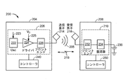
図2は、別の例示的な態様によるワイヤレス電力伝達システム200の機能ブロック図である。システム200は、送信機204と受信機208とを含み得る。送信機204(本明細書では、電力伝達ユニット、PTUとも呼ばれる)は、発振器222と、ドライバ回路224と、フロントエンド回路226とを含み得る送信回路206を含み得る。発振器222は、周波数制御信号223に応答して調整され得る所望の周波数(たとえば、基本周波数)において(発振信号としても知られている)発振器信号を生成するように構成され得る。発振器222は、ドライバ回路224に発振器信号を提供してもよい。ドライバ回路224は、入力電圧信号(VD)225に基づいて、たとえば、電力送信素子214の共振周波において電力送信素子214を駆動するように構成されてもよい。ドライバ回路224は、発振器222から方形波を受信し、駆動信号出力として正弦波を出力するように構成されたスイッチング増幅器であってよい。
FIG. 2 is a functional block diagram of a wireless
フロントエンド回路226は、高調波または他の不要な周波数をフィルタ除去するように構成されたフィルタ回路を含み得る。フロントエンド回路226は、送信機204のインピーダンスを電力送信素子214のインピーダンスに整合させるように構成された整合回路を含み得る。以下でより詳細に説明するように、フロントエンド回路226は、電力送信素子214を有する共振回路を生み出すための同調回路を含み得る。電力送信素子214を駆動した結果として、電力送信素子214は、バッテリー236を充電するかまたは場合によっては負荷に電力供給するのに十分なレベルで電力をワイヤレスに出力するためのワイヤレス場205を生成することができる。
送信機204は、送信回路206に動作可能に結合され、送信回路206の1つもしくは複数の態様を制御するかまたは電力の伝達の管理に関連する他の動作を遂行するように構成されたコントローラ240をさらに含み得る。コントローラ240は、マイクロコントローラまたはプロセッサであってもよい。コントローラ240は、特定用途向け集積回路(ASIC)として実装されてもよい。コントローラ240は、直接または間接的に、送信回路206の各構成要素に動作可能に接続されてもよい。コントローラ240は、送信回路206の構成要素の各々から情報を受信し、受信された情報に基づいて算出を実行するようにさらに構成され得る。コントローラ240は、その構成要素の動作を調整し得る構成要素の各々のための制御信号(たとえば、信号223)を生成するように構成され得る。したがって、コントローラ240は、それによって実行された演算の結果に基づいて、電力伝達を調整または管理するように構成されてよい。送信機204は、たとえば、コントローラ240にワイヤレス電力伝達の管理に関する機能などの特定の機能を実行させるための命令などのデータを記憶するように構成されたメモリ(図示せず)をさらに含み得る。
A
受信機208(本明細書では、電力受信ユニット、PRUとも呼ばれる)は、フロントエンド回路232と、整流器回路234とを含み得る受信回路210を含み得る。フロントエンド回路232は、受信回路210のインピーダンスを電力受信素子218のインピーダンスに整合させるように構成された整合回路を含み得る。以下で説明するように、フロントエンド回路232は、電力受信素子218を有する共振回路を生み出すための同調回路をさらに含み得る。整流器回路234は、図2に示すように、バッテリー236を充電するために、AC電力入力からDC電力出力を生成することができる。受信機208および送信機204は、追加として、別個の通信チャネル219(たとえば、Bluetooth(登録商標)、Zigbee、セルラーなど)上で通信し得る。受信機208および送信機204は、代替的に、ワイヤレス場205の特性を使用する帯域内シグナリングを介して通信し得る。
The receiver 208 (also referred to herein as a power receiving unit, PRU) may include a receiving
受信機208は、送信機204によって送信され、受信機208によって受信される電力量がバッテリー236を充電するのに適切であるかどうかを判定するように構成され得る。いくつかの態様では、送信機204は、エネルギー伝達を行うための直接場結合係数(k)を有する主に非放射性の場を生成するように構成され得る。受信機208は、ワイヤレス場205に直接結合してもよく、出力回路または受信回路210に結合されたバッテリー(または負荷)236によって蓄積または消費される出力電力を生成することができる。
The
受信機208は、ワイヤレス電力受信機208の1つまたは複数の態様を管理するための、上記で説明した送信コントローラ240と同様に構成されたコントローラ250をさらに含み得る。受信機208は、たとえば、ワイヤレス電力伝達の管理に関する機能などの特定の機能をコントローラ250に実行させるための命令などのデータを記憶するように構成されたメモリ(図示せず)をさらに含み得る。
The
上記で説明したように、送信機204および受信機208は、ある距離だけ離されてもよく、送信機204と受信機208との間の伝送損失を最小限に抑えるように相互共振関係に従って構成されてもよい。
As explained above,
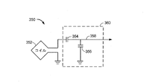
図3は、例示的な態様による、図2の送信回路206または受信回路210の一部分の概略図である。図3に示すように、送信回路または受信回路350は、電力送信素子または電力受信素子352と、同調回路360とを含み得る。電力送信素子または電力受信素子352はまた、アンテナもしくは「ループ」アンテナと呼ばれるか、またはそれらとして構成され得る。「アンテナ」という用語は、一般に、別のアンテナへの結合のためのエネルギーをワイヤレスに出力または受信することができる構成要素を指す。電力送信素子または電力受信素子352はまた、本明細書では「磁気」アンテナ、または誘導コイル、共振器、もしくは共振器の一部と呼ばれるか、またはそれらとして構成され得る。電力送信素子または電力受信素子352はまた、電力をワイヤレスに出力または受信するように構成されるタイプのコイルまたは共振器と呼ばれる場合がある。本明細書で使用する電力送信素子または電力受信素子352は、電力をワイヤレスに出力および/または受信するように構成されるタイプの「電力伝達構成要素」の例である。電力送信素子または受信素子352は、空芯、またはフェライトコアなどの物理コア(この図には示さず)を含み得る。
FIG. 3 is a schematic diagram of a portion of the transmit
電力送信素子または電力受信素子352が同調回路360を有する共振回路または共振器として構成されるとき、電力送信素子または電力受信素子352の共振周波数は、インダクタンスおよびキャパシタンスに基づき得る。インダクタンスは、単に、電力送信素子または電力受信素子352を形成するコイルおよび/または他のインダクタによって生み出されるインダクタンスであってもよい。キャパシタンス(たとえば、キャパシタ)は、所望の共振周波数で共振構造を生み出すように同調回路360によって提供されてもよい。非限定的な例として、同調回路360は、共振回路を生み出すように送信および/または受信回路350に追加され得る、キャパシタ354およびキャパシタ356を備えてもよい。
When the power transmitting element or
同調回路360は、電力送信素子または電力受信素子352を有する共振回路を形成するための他の構成要素を含み得る。別の非限定的な例として、同調回路360は、回路350の2つの端子間に並列に配置されたキャパシタ(図示せず)を含んでもよい。さらに他の設計が可能である。いくつかの態様では、フロントエンド回路226内の同調回路は、フロントエンド回路232内の同調回路と同じ設計(たとえば、360)を有し得る。他の態様では、フロントエンド回路226は、フロントエンド回路232とは異なる同調回路設計を使用してよい。
Tuning circuit 360 may include other components for forming a resonant circuit having a power transmitting element or a
電力送信素子に関しては、電力送信素子または電力受信素子352の共振周波数にほぼ対応する周波数を有する信号358は、電力送信素子または電力受信素子352への入力であってもよい。電力受信素子に関しては、電力送信素子または電力受信素子352の共振周波数にほぼ対応する周波数を有する信号358は、電力送信素子または電力受信素子352からの出力であってもよい。本明細書で開示する態様は、一般に共振ワイヤレス電力伝達を対象とする場合があるが、当業者は、本明細書で開示する態様がワイヤレス電力伝達のための非共振実装形態において使用され得ることを諒解されよう。
With respect to the power transmitting element, a
いくつかの態様では、電力(たとえば、エネルギー)がワイヤレス電力送信機(たとえば、送信機204)からワイヤレス電力受信機(たとえば、受信機208)を備えたデバイス(たとえば、医療用インプラント)によってワイヤレスに受信されるとき、正確な電力量が送信機204から受信機208に伝達されることを確実にするための電力制御の方法が存在し得る。たとえば、受信機208を備えたデバイスは、特定の電圧(たとえば、4.2V)で動作/充電するように構成され得る。しかしながら、送信機204による固定強度のワイヤレス場205の生成は、受信機208において所望の電圧を生成しない場合がある。たとえば、所与の強度のワイヤレス場205で送信機204と受信機208との間で伝達される電力量は、送信機204と受信機208との間の距離(および/または、それらの間の材料など、他の要因)に基づいて異なり得る。したがって、デバイスに対して受信機208によって生成される電力(たとえば、電圧)は、送信機204からの同じ強度のワイヤレス場205に対する1つまたは複数の要因に基づいて変化し得る。たとえば、医療用インプラントデバイスは、人物の中に、異なる組織タイプおよび厚みを有する皮膚の下の様々な距離/位置に埋め込むことができる。したがって、本明細書で論じるいくつかの態様は、ワイヤレス電力受信機を備えたデバイスが正確な電力供給を受けることを確実にするために、ワイヤレス電力送信機からワイヤレス電力受信機に伝達される電力を制御するためのシステムおよび方法に関する。
In some aspects, power (e.g., energy) is wirelessly transmitted from a wireless power transmitter (e.g., transmitter 204) to a device (e.g., medical implant) with a wireless power receiver (e.g., receiver 208). There can be a method of power control to ensure that the correct amount of power is transmitted from the
いくつかの態様では、ワイヤレスに電気供給されているデバイスにおける電力(たとえば、電圧)が所望の電力(たとえば、所望の電圧)であることを確実にするために、ワイヤレス場205の強度を調整するための閉ループ電力制御方式を採用することができる。たとえば、いくつかの態様では、ワイヤレス受信機208は、整流器234における電圧など、受信機208において受信される電力の電力レベルをアクティブに判定するように構成され得る。たとえば、コントローラ250は、整流器234における電圧を監視するように構成され得る。整流器234における電圧が所望の電圧レベルの範囲を超えるかまたはそれを下回るかに応じて、(たとえば、コントローラ250によって制御される)ワイヤレス受信機208は、ワイヤレス場205の強度が増大されるべきかまたは低減されるべきかを示すフィードバック情報(たとえば、制御信号)を(たとえば、通信チャネル219またはワイヤレス場205を使用してバンド内シグナリングを介して)をワイヤレス送信機204に送信することができる。整流器234における電圧が所望の電圧レベルの範囲内でない場合、何の制御信号も送られなくてよい。ワイヤレス送信機204は、制御信号を受信し、それに応じて、(たとえば、コントローラ240からの制御により)ワイヤレス場205の強度を調整することができる。
In some aspects, the strength of the
いくつかの態様では、受信機208における電力レベルは、非常に低い場合があり、したがって、フィードバック情報を送信するためのより高い電力技術(たとえば、通信チャネル219またはバンド内シグナリングを介したより高い電力通信)は実現可能でない場合がある。具体的には、受信機208を備えたデバイスは、フィードバック情報を送信機204にアクティブに送信することができない場合があり、したがって、送信機204は、充電されているデバイスにおける電圧に関する情報を有さず、デバイスが最新技法を使用して正確な電圧で動作していることを確実にするために、ワイヤレス場205の強度を調整できない場合がある。たとえば、デバイスにおけるバッテリーが完全に充電されている場合、電力がデバイスにおけるワイヤレス受信機208によってワイヤレス電力送信機204から最初に受信されるときと、デバイスがブートアップして、(たとえば、無線を介して)通信チャネル219または(たとえば、電力を必要とする、コントローラ250による制御により)バンド内シグナリングを使用することが可能なときとの間に、フィードバック情報を送信機204に送信するための時間の遅延(たとえば、10秒)が存在し得る。場合によっては、デバイスは、フィードバック情報を送信するための手段(たとえば、無線)を有さない場合がある。
In some aspects, the power level at
したがって、本開示のいくつかの態様は、ワイヤレス電力送信機の電力レベルを制御するためのワイヤレス電力伝達のためのフィードバック機構に関する。具体的には、論じたように、受信機208は、AC電力入力からDC電力出力を生成するための整流器234を含む。本開示のいくつかの態様は、受信機208における電圧レベルに関するフィードバック情報を提供するように設計された整流器に関する。具体的には、いくつかの態様は、整流の間に高調波を生成し、そのような高調波を使用して送信機204と通信するように構成された受信機208に関する。たとえば、受信機208は、受信機208において十分な電力が存在することを示す特定の高調波、または何らかの他の情報(たとえば、受信機208の他のステータス情報)さえ生成することができる。いくつかの態様では、送信機204は、(たとえば、送信素子214など、アンテナを介して)そのような高調波を検出することができる。いくつかの態様では、高調波の検出は、ワイヤレス電力を受信するように構成され、かつワイヤレス電力を受信することが可能なデバイス(たとえば、受信機208)が存在し、ワイヤレス電力を吸収していることを送信機204に示すことができる。いくつかの態様では、高調波の検出は、論じたように他の情報を示すことができる。
Accordingly, certain aspects of the present disclosure relate to a feedback mechanism for wireless power transfer for controlling the power level of a wireless power transmitter. Specifically, as discussed,
図4は、本開示のいくつかの態様による整流器を含む受信回路400の一部分の概略図である。受信回路400は、受信機208の一部に対応し得る。示すように、受信回路400は、受信アンテナ(たとえば、インダクタ、コイル、受信素子352など)402を含む。さらに、受信回路400は、結合キャパシタ(CC)404と分路共振キャパシタ(CS)406(たとえば、300pF)とを含む。CC404は、大きな値(たとえば、260pF)のキャパシタであってよく、AC電力を整流器420に結合するように構成されてよい。キャパシタ404および406は、所望の共振周波数で共振構造を生み出すために提供され得る。
FIG. 4 is a schematic diagram of a portion of a
受信回路400は、伝達された電力をフィルタリング/平滑化するように構成され得るフィルタキャパシタ(Cf)408(たとえば、.01μF)をさらに含む。さらに、受信回路400によって電力供給された負荷(たとえば、バッテリー、インプラントデバイスなど)の等価抵抗RL(たとえば、1kΩ)が示されている。いくつかの態様では、受信回路400は、電圧クランプとして働くように構成されたオプションのダイオード410(たとえば、ツェナーダイオー)を含む。さらに、キャパシタおよびアンテナの寄生抵抗RP(たとえば、1Ω)が示されている。
Receive
整流器420は、直列に結合された第1のダイオード422と第2のダイオード424とを含む。さらに、整流器420は、第2のダイオード424に並列に結合された抵抗器(RS)426(たとえば、100kΩなど、高い値の抵抗器)を含み、RS426の第1の端子は、第2のダイオード424の第1の端子に結合され、RS426の第2の端子は、第2のダイオード424の第2の端子に結合される。いくつかの態様では、第1のダイオード422および第2のダイオード424は、電圧ダブラ整流器またはその部分として働くように構成される。
整流器420の特性は、受信回路400における電圧レベル(たとえば、受信回路400に接続された負荷における電圧)に関するフィードバック情報として使用され得る。たとえば、ワイヤレス電力送信機(たとえば、送信機204)からアンテナ402によって受信された電力が上昇すると、第1のダイオード422および第2のダイオード424の非線形特性は、第1のダイオード422および第2のダイオード424に、電圧レベルと共に変化する高調波を生成させる。第1のしきい値(たとえば、.5V)を下回る、アンテナ402によって受信される電力レベルにおいて、第1のダイオード422も第2のダイオード424もRS426として導通せず、第1のダイオード422と第2のダイオード424との間のノードにおける電圧を低く維持しない。したがって、受信回路400の負荷における電圧は実質的に存在しない。
The characteristics of the
ワイヤレス電力送信機(たとえば、送信機204)からアンテナ402によって受信される電力が、第1のしきい値を超えるが、第2のしきい値を下回って(たとえば、RL上の電圧を.5Vを越えて)上昇すると、第2のダイオード424は導通し始める。具体的には、第2のダイオード424に並列なRS426は、第2のダイオード424に第1のダイオード422よりも低い電力レベルで導通させる。第2のダイオード424が導通すると、(たとえば、特定の基本周波数で受信された)受信された電力信号の第2高調波が第2のダイオード424によって生成され、アンテナ402を介して放射し戻される。第2高調波のそのような生成は、第2のダイオード424の特性に基づき、アクティブな回路によって別個に生成されないことに留意されたい。本明細書でさらに論じるように、アンテナ402から放射し戻されたそのような第2高調波は、ワイヤレス電力送信機(たとえば、送信機204)によって検出可能であり得る。第2のダイオード424のみが導通する電力レベルにおいて、受信回路400の負荷における電圧レベルは所望の電圧レベルを下回る場合がある。
The power received by the
さらに、ワイヤレス電力送信機(たとえば、送信機204)からアンテナ402によって受信された電力が第2のしきい値を超えて上昇すると、第2のダイオード424に加えて、第1のダイオード422が導通し始める。具体的には、第1のダイオード422と第2のダイオード424との間のノードにおける電圧は第1のダイオード422および第2のダイオード424のクランピングアクション(clamping action)によって設定されるため、これらの高い電力レベルにおいて回路上のRS426の影響は最小になる。第1のダイオード422および第2のダイオード424は、受信された電力信号の第3高調波を生成する。第3高調波は、アンテナ402を介して放射し戻される。第3高調波のそのような生成は、第1のダイオード422および第2のダイオード424の特性に基づき、アクティブな回路によって別個に生成されないことに留意されたい。本明細書でさらに論じるように、そのような第3高調波は、ワイヤレス電力送信機(たとえば、送信機204)によって検出可能であり得る。第1のダイオード422および第2のダイオード424が導通する電力レベルにおいて、受信回路400の負荷における電圧レベルは所望の電圧レベルであるか、またはそれに近い場合がある。
In addition, in addition to the
ワイヤレス電力送信機、たとえば、送信機204は、アンテナ402から放射された(たとえば、反射された)第2高調波および第3高調波を検出し、それらの信号に基づいて、ワイヤレス電力送信機によって放出された充電場の電力を制御するように構成され得る。いくつかの態様では、ワイヤレス電力送信機は、第2高調波および第3高調波の各々またはその比率のレベルを利用して、充電場の電力を制御することができる。
A wireless power transmitter, e.g.,
いくつかの態様では、送信機204は、受信機208に送信するために、クリーンな(最小の2次高調波または3次高調波の)ワイヤレス場205を生成するように構成され得る。たとえば、フロンドエンド回路226は、ワイヤレス場205を生成するために利用される信号から2次高調波および3次高調波をフィルタ除去するように構成されたフィルタ回路を含み得る。そのような第2高調波および第3高調波をフィルタ除去することは、送信機204からのそのような第2高調波および第3高調波が受信機208によって生成される第2高調波および第3高調波と間違えられることを防ぐのに役立ち得る。ワイヤレス場205の電力レベルが増大し、第1のダイオード422および/または第2のダイオード424が導通し始めると、送信機204は、受信機208から放射された高調波を受信することができる。送信機204は、放射された高調波を受信するためのワイヤレス場205を生成するために使用されるのと同じ電力送信素子214を利用することができるか、または異なる素子(たとえば、アンテナ、コイルなど)を使用することができる。放射された高調波は、ワイヤレス場205など、他の信号を含み得る、受信機208によって生成されたワイヤレス場の部分として受信され得る。本明細書で論じるように、送信機204は、受信された高調波に基づいて、ワイヤレス電力送信機204によって放出されたワイヤレス場205の電力を制御することができる。
In some aspects, the
図5は、本開示のいくつかの態様による送信回路500の一部分のブロック図である。送信回路500は、送信機204の一部に対応し得る。送信回路500は、受信機208から放射された高調波を受信するために利用され得る。示すように、送信回路500は、アンテナ(たとえば、電力送信素子214、別個のアンテナ、コイルなど)502を含む。アンテナ502から受信された信号は、増幅器503によって増幅され、分割されて、それぞれ、第2高調波および第3高調波に関して選択する2つの別個のフィルタ(たとえば、帯域フィルタ)を通過し得る。具体的には、受信された信号は、示すように、第1のフィルタ504を通過し得、第1のフィルタ504は、第2高調波に対応する、信号内の周波数を通すためのバンドパスフィルタを備え得る。加えて、受信された信号は、示すように、第2のフィルタ506を通過し得、第2のフィルタ506は、第3高調波に対応する、信号内の周波数を通すためのバンドパスフィルタを備え得る。
FIG. 5 is a block diagram of a portion of a transmit
第1のフィルタ504および第2のフィルタ506の各々の出力は、次いで、受信された第2高調波および第3高調波の相対強度を検出するために、1つまたは複数の信号プロセッサ(たとえば、信号検出器)508に送られ得る。いくつかの態様では、別個の信号プロセッサ508を使用して、第2高調波および第3高調波の各々を検出することができる。いくつかの態様では、単一の信号プロセッサ508は、第2高調波と第3高調波の両方を検出するように構成され得る。ワイヤレス場205の電力を調整するために(たとえば、1つまたは複数のしきい値、絶対インジケータ、強度に比例する電圧出力などに対する)強度の指示が信号プロセッサ508からコントローラ240(または、別のプロセッサ)に送られ得る。いくつかの態様では、信号プロセッサ508およびコントローラ240は、単一のチップ上で実装されてよいか、または別個のチップ上で実装されてもよい。
The outputs of each of the
コントローラ240は、受信機208から受信された第2高調波および第3高調波の強度の指示に基づいて、ワイヤレス場205の電力を制御することができる。具体的には、コントローラ240は、いくつかの態様では、受信された第2高調波の強度が第1のしきい値を超え、受信された第3高調波の強度が第2のしきい値を超えるまで、デバイスに最初に電力供給するとき(たとえば、送信機204と受信機208との間の最初の結合時に)ワイヤレス場205の電力を増分的に増大させるように構成され得る。コントローラ240は、次いで、ワイヤレス場205の強度を保持するか、または受信機208が完全に電力供給されるまで、知られている量だけワイヤレス場205の強度を増大させることができる。
The
図6は、本開示のいくつかの態様による、ワイヤレス電力伝達のための例示的な動作600のフローチャートである。
FIG. 6 is a flowchart of an
605において、送信機204は、電力を受信機208に伝達するための初期電力レベル(たとえば、最低電力レベル)でワイヤレス場205を生成することができる。いくつかの態様では、ワイヤレス場205を生成する前に、送信機204は、生成されることになるワイヤレス場205の高調波における高周波レベル(たとえば、第2高調波および第3高調波)を測定することができる。いくつかの態様では、ワイヤレス電力受信機の検出、ワイヤレス場205の電力レベルの調整などに関する第2高調波および第3高調波のしきい値は、測定された高調波レベルに基づいて調整され得る(たとえば、測定された高調波レベルをベースラインとして使用し、特定のしきい値だけ増大を求める)。610において、送信機204は、受信機208から放射された高調波を含み得る、受信された信号を測定することができる。いくつかの態様では、送信機204は、受信機208から放射された高調波を測定しながら、ワイヤレス場205を生成し続けることができる。いくつかの態様では、送信機204は、受信機208から放射された高調波を測定しながら、(たとえば、ドライバ224の電源を切断することによって)ワイヤレス場205の生成を一時的に中断し、次いで、ワイヤレス場205の生成に戻ることができる。615において、送信機204は、受信された信号内の2次高調波が第1のしきい値を超えるかどうかを判定する。2次高調波が第1のしきい値を越えない場合、620において、送信機204は、ワイヤレス場205の電力レベルを上へと増分し、615に戻る。
At 605, the
2次高調波が第1のしきい値を超える場合、625において、送信機204は、受信された信号に関する3次高調波が第2のしきい値を超えるかどうかを判定する。3次高調波が第2のしきい値を越えない場合、630において、送信機204は、ワイヤレス場205の電力レベルを上へと増分し、625に戻る。
If the second harmonic exceeds the first threshold, at 625, the
3次高調波が第2のしきい値を超える場合、動作600は終了し得る。送信機204は、ワイヤレス場205の強度を保持するか、またはワイヤレス場205の強度を知られている量だけ増大させることができる。具体的には、3次高調波が第2のしきい値を超えると、受信機208のダイオードは導通しており、受信機208を備えたデバイスが起動するために十分な電力が受信機208において受信される。送信機204および受信機208のさらなる制御は、フィードバックのための他の手段および技法によって達成され得る。
If the third harmonic exceeds the second threshold,
いくつかの態様では、図4に関して論じた受信回路400は、受動回路を使用して高調波を生成し、高調波を生成するために能動回路(たとえば、スイッチ)を必要としないように構成され得る。したがって、受信回路400は、論じたように、高調波を生成するようにそのような能動回路を制御するために、追加の電力を必要としなくてよく、非常に低い電力レベルで作動することができる。
In some aspects, the receive
いくつかの他の態様では、受信機(たとえば、受信機208)における受信回路は、送信機204と通信するために受信機208において高調波を選択的に生成するために同じ能動回路を有するように設計され得る。送信機204は、受信機208によって生成される高調波を(たとえば、送信回路500を利用して)検出し、受信された高調波が通信された情報を示すものと解釈することができる。具体的には、一部の能動回路を利用することによって、高調波がいつどのように生成されるかが受信機208によってアクティブに制御され、したがって、ほとんどすべての情報がそのような高調波によって示され得る。たとえば、いくつかの態様では、高調波が単に存在するか否かは、単一の情報ビットを示し得る(たとえば、受信機208が十分な電力を有するか否か、受信機が208正常に機能しているか否か、など)。いくつかの態様では、高調波は、追加の情報(たとえば、異なる変調または変動に対応する情報ビット)を示すために修正(たとえば変調または変更)され得る。たとえば、いくつかの態様では、高調波は、能動ダイオード整流経路、または整流経路内の構成要素(たとえば、スイッチ、抵抗器など)を通して整流するための他の修正を調整することによって修正され得る。たとえば、直列抵抗、負荷、トポロジー変更、共振器の再同調などを(たとえば、スイッチを選択的に開閉することによって)切り替えることは、すべて生み出された高調波を修正するために実行され得る。いくつかの態様では、高調波は、受信機208の能動整流器の1つまたは複数のスイッチを(たとえば、スイッチを選択的に開閉することによって)切り替えることによって高調波を変調することにより修正され得る。高調波は、受信機208における電力レベルを送信機204にシグナリングするためにアクティブ整流器によって生成されたDC電流の電力レベルに基づいて変調され得る。本明細書で説明する技法は、いくつかの態様では、情報を通信するための他のアクティブな回路技法よりも依然として低電力でありながら、受信機208と送信機204との間で情報を通信するために、高調波を選択的に生成および/または修正するために低電力消費技法を利用することができる。
In some other aspects, the receiving circuit at the receiver (eg, receiver 208) may have the same active circuit to selectively generate harmonics at the
いくつかの態様では、送信機204は、ワイヤレス場205を生成するときに奇数の高調波をやはり生成することができるため、受信機208によって生成される高調波は、受信機208から高調波を受信するための送信機204における低信号対雑音比を回避するために奇数の高調波とは対照的に偶数の高調波(たとえば、2次、4次など)であってよい。したがって、いくつかの態様では、受信機208は、そのような偶数の高調波を生成するために、非線形構成要素(たとえば、逆バイアスされたダイオード接合(たとえば、ダイオードまたはFET)など、電圧に応じたキャパシタンスを備えたキャパシタ)を利用することができる。
In some aspects, the
図7は、本開示のいくつかの態様による、高調波を選択的に生成するように構成された受信回路700の一部分の概略図である。受信回路700は、受信機208の一部に対応し得る。具体的には、受信回路700は、示すように、図4の受信回路400とほとんど同じ構成要素を有し得る。しかしながら、受信回路700は、抵抗器726を第2のダイオード724に並列に(スイッチ728を選択的に開閉することによって)選択的に結合するように構成されたスイッチ(たとえば、トランジスタ)728をさらに含み得る。したがって、受信回路700は、抵抗器726が第2のダイオード724に並列に結合されているか否かに基づいて高調波(たとえば、第2高調波および第3高調波)を選択的に生成するように構成され得る。たとえば、いくつかの態様では、抵抗器726が第2のダイオード724に並列に結合されているとき、高調波が生成され得、抵抗器726が第2のダイオード724に並列に結合されていないとき、高調波は生成され得ない。スイッチ728は、コントローラ250などのコントローラによって制御され得る。
FIG. 7 is a schematic diagram of a portion of a receive
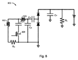
図8は、本開示のいくつかの態様による、高調波を選択的に生成するように構成された受信回路800の別の部分の概略図である。受信回路800は、受信機208の一部に対応し得る。具体的には、受信回路800は、示すように、図4の受信回路400とほとんど同じ構成要素を有し得る。しかしながら、受信回路800は、受信回路400の抵抗器426を含まなくてよい。さらに、受信回路800は、受信アンテナ802に並列に選択的に結合されたキャパシタ824を追加で含み得る。具体的には、スイッチ(たとえば、トランジスタ)828は、キャパシタ824に直列に結合され、キャパシタ824を受信アンテナ802に並列に(たとえば、スイッチ828を選択的に開閉することによって)選択的に結合するように構成され得る。さらに、受信回路800は、アンテナ802に直列に結合されたインダクタ826を追加で含んでよく、キャパシタ824の結合点は、受信アンテナ802とインダクタ826との間である。キャパシタ824およびインダクタ826は、受信回路800からの高調波を阻止することまたは通すことができる電磁干渉(EMI)フィルタとして働くように構成され得る。具体的には、キャパシタ824をアンテナ802に並列に選択的に結合することまたは分離することは、EMIフィルタとしての効果を断つかまたは修正することができ、したがって、高調波を阻止することまたは通すことができる。たとえば、キャパシタ824がアンテナ802に並列に結合されている場合、インダクタ826およびキャパシタ824は、高調波が生成されることを阻止し得る。しかしながら、キャパシタ824がアンテナ802に並列に結合されていない場合、受信回路800は高調波を生成することができる。スイッチ828は、コントローラ250などのコントローラによって制御され得る。
FIG. 8 is a schematic diagram of another portion of a
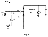
図9は、本開示のいくつかの態様による、高調波を選択的に生成するように構成された受信回路900の別の部分の概略図である。受信回路900は、受信機208の一部に対応し得る。具体的には、受信回路900は、示すように、図4の受信回路400とほとんど同じ構成要素を有し得る。しかしながら、受信回路900は、受信回路400の抵抗器426を含まなくてよい。さらに、受信回路900は、受信アンテナ902に並列に結合されたキャパシタ924を追加で含み得る。いくつかの態様では、スイッチ(たとえば、トランジスタ)928は、キャパシタ924に直列に結合され、キャパシタ924を受信アンテナ902に並列に(たとえば、スイッチ928を選択的に開閉することによって)選択的に結合するように構成され得る。キャパシタ924は、非線形キャパシタンスを有し得る(たとえば、キャパシタ924は、トランスキャップ(transcap)可変キャパシタ、バラクタ/ダイオード、FETなどのうちの1つであってよい)。したがって、キャパシタ924がアンテナ902に並列に結合されている場合、受信回路900は偶数の高調波を生成することができる。しかしながら、キャパシタ924がアンテナ902に並列に結合されていない場合、受信回路900は高調波を生成することができない。スイッチ928は、コントローラ250などのコントローラによって制御され得る。別の態様では、受信回路900がスイッチ928を含む代わりに、キャパシタ924のキャパシタンスは、高調波を選択的に生成するために調整され得る(たとえば、キャパシタ924は可変キャパシタを含み得る)。キャパシタ924のキャパシタンスは、コントローラ250などのコントローラによって制御され得る。
FIG. 9 is a schematic diagram of another portion of a
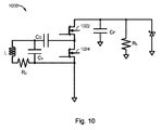
図10は、本開示のいくつかの態様による、高調波を選択的に生成するように構成された受信回路1000の別の部分の概略図である。受信回路1000は、受信機208の一部に対応し得る。具体的には、受信回路1000は、示すように、図4の受信回路400とほとんど同じ構成要素を有し得る。しかしながら、受信回路1000は、受信回路400の抵抗器426を含まなくてよい。さらに、受信回路1000は、能動整流器を形成する第1のダイオード422および第2のダイオード424を含まなくてよく、代わりに、トランジスタ1022および1024を使用して示すように、アクティブ整流器を含む。いくつかの態様では、トランジスタ1022および1024の切替えタイミング(開閉)は、送信機204から受信された電力の大部分を依然として整流しながら、高調波を変調するように修正され得る。いくつかの他の態様では、トランジスタ1022および1024は、整流を選択的に有効化および無効化するために選択的に有効化および無効化され得る。整流が有効化されるとき、高調波が生成され得る。整流が無効化されるとき、高調波は生成され得ない。トランジスタ1022および1024は、コントローラ250などのコントローラによって制御され得る。
FIG. 10 is a schematic diagram of another portion of a
送信機204は、回路700〜1000のいずれかによって生成されたそのような高調波を受信し、受信された高調波に基づいてアクションを実行する(たとえば、ワイヤレス場205の強度を調整する)ように構成され得る。たとえば、上記で論じたように、受信機208のコントローラ250は、送信機204がアクションを実行するために利用することができる情報を送信機204に通信するために高調波を選択的に生成するように構成され得る。
The
上記で説明した方法の様々な動作は、対応する機能を実行できる任意の好適な手段によって実行され得る。この手段は、限定はしないが、回路、特定用途向け集積回路(ASIC)、またはプロセッサを含む、様々なハードウェアおよび/またはソフトウェア構成要素および/またはモジュールを含んでもよい。一般に、図に示す動作がある場合、それらの動作は、同様の番号を付された対応する同等のミーンズプラスファンクション構成要素を有し得る。 The various operations of the methods described above may be performed by any suitable means that can perform the corresponding function. This means may include various hardware and / or software components and / or modules, including but not limited to circuits, application specific integrated circuits (ASICs), or processors. In general, where there are operations shown in the figures, those operations may have corresponding equivalent means-plus-function components numbered similarly.
本明細書で使用する「判定すること」という用語は、幅広い様々なアクションを包含する。たとえば、「判定すること」は、算出すること、計算すること、処理すること、導出すること、調査すること、ルックアップすること(たとえば、テーブル、データベースまたは別のデータ構造においてルックアップすること)、確認することなどを含んでもよい。また、「判定する」は、受信する(たとえば、情報を受信する)、アクセスする(たとえば、メモリ内のデータにアクセスする)などを含み得る。また、「判定する」は、解決する、選択する、選出する、確立するなどを含み得る。 As used herein, the term “determining” encompasses a wide variety of actions. For example, “determining” is calculating, calculating, processing, deriving, examining, looking up (eg, looking up in a table, database or another data structure) , And so on. Also, “determining” can include receiving (eg, receiving information), accessing (eg, accessing data in a memory) and the like. Also, “determining” can include resolving, selecting, selecting, establishing, and the like.
本明細書で使用するとき、項目の列挙「のうちの少なくとも1つ」を指す句は、単一のメンバーを含むそれらの項目の任意の組合せを指す。一例として、「a、b、またはcのうちの少なくとも1つ」は、a、b、c、a-b、a-c、b-c、およびa-b-c、ならびに複数の同じ要素を有する任意の組合せ(たとえば、a-a、a-a-a、a-a-b、a-a-c、a-b-b、a-c-c、b-b、b-b-b、b-b-c、c-c、およびc-c-c、またはa、b、およびcの任意の他の順序)をカバーするものとする。 As used herein, a phrase referring to “at least one of” a list of items refers to any combination of those items including a single member. By way of example, “at least one of a, b, or c” includes a, b, c, ab, ac, bc, and abc, and any combination having a plurality of the same elements (eg, aa, aaa , Aab, aac, abb, acc, bb, bbb, bbc, cc, and ccc, or any other order of a, b, and c).
本開示に関して説明した様々な例示的な論理ブロック、モジュール、および回路は、汎用プロセッサ、デジタル信号プロセッサ(DSP)、ASIC、フィールドプログラマブルゲートアレイ(FPGA)もしくは他のプログラマブル論理デバイス(PLD)、個別ゲートもしくはトランジスタ論理、個別ハードウェア構成要素、または、本明細書に記載の機能を実行するように設計されたそれらの任意の組合せを用いて実装または実行されてもよい。汎用プロセッサは、マイクロプロセッサであってよいが、代替として、プロセッサは、任意の市販のプロセッサ、コントローラ、マイクロコントローラ、または状態機械であってもよい。プロセッサはまた、コンピューティングデバイスの組合せ、たとえば、DSPおよびマイクロプロセッサの組合せ、複数のマイクロプロセッサ、DSPコアと連携する1つもしくは複数のマイクロプロセッサ、または任意の他のそのような構成として実装されてもよい。 The various exemplary logic blocks, modules, and circuits described in connection with this disclosure are general purpose processors, digital signal processors (DSPs), ASICs, field programmable gate arrays (FPGAs) or other programmable logic devices (PLDs), individual gates. Or it may be implemented or implemented using transistor logic, discrete hardware components, or any combination thereof designed to perform the functions described herein. A general purpose processor may be a microprocessor, but in the alternative, the processor may be any commercially available processor, controller, microcontroller or state machine. The processor may also be implemented as a combination of computing devices, eg, a DSP and microprocessor combination, multiple microprocessors, one or more microprocessors in conjunction with a DSP core, or any other such configuration. Also good.
本明細書で開示される方法は、説明された方法を実現するための1つまたは複数のステップまたはアクションを含む。方法ステップおよび/またはアクションは、特許請求の範囲から逸脱することなく互いに入れ替えられ得る。言い換えれば、ステップまたはアクションの特定の順序が指定されない限り、特定のステップおよび/またはアクションの順序および/または使用は、特許請求の範囲から逸脱することなく修正され得る。 The methods disclosed herein include one or more steps or actions for achieving the described method. The method steps and / or actions may be interchanged with one another without departing from the scope of the claims. In other words, unless a specific order of steps or actions is specified, the order and / or use of specific steps and / or actions may be modified without departing from the scope of the claims.
説明した機能は、ハードウェア、ソフトウェア、ファームウェア、またはそれらの任意の組合せで実装されてもよい。ハードウェアとして実装される場合、例示的なハードウェア構成は、ワイヤレスノード内の処理システムを備え得る。処理システムは、バスアーキテクチャを用いて実装され得る。バスは、処理システムの特定の用途および全体的な設計制約に応じて、任意の数の相互接続バスおよびブリッジを含んでもよい。バスは、プロセッサ、機械可読媒体、およびバスインターフェースを含む様々な回路を互いにリンクする場合がある。バスインターフェースは、とりわけ、バスを介してネットワークアダプタを処理システムに接続するために使用され得る。ネットワークアダプタは、物理(PHY)層の信号処理機能を実装するために使用され得る。ユーザ端末の場合、ユーザインターフェース(たとえば、キーパッド、ディスプレイ、マウス、ジョイスティックなど)をバスに接続することもできる。バスは、タイミングソース、周辺機器、電圧調整器、電力管理回路などの様々な他の回路をリンクさせる場合もあり、これは当技術分野ではよく知られているので、これ以上説明しない。 The functions described may be implemented in hardware, software, firmware, or any combination thereof. When implemented as hardware, an exemplary hardware configuration may comprise a processing system within a wireless node. The processing system can be implemented using a bus architecture. The bus may include any number of interconnect buses and bridges depending on the particular application of the processing system and the overall design constraints. A bus may link various circuits including a processor, a machine-readable medium, and a bus interface together. The bus interface can be used, among other things, to connect the network adapter to the processing system via the bus. Network adapters can be used to implement physical (PHY) layer signal processing functions. In the case of a user terminal, a user interface (eg, keypad, display, mouse, joystick, etc.) can also be connected to the bus. The bus may link various other circuits such as timing sources, peripherals, voltage regulators, power management circuits, etc., which are well known in the art and will not be described further.
処理システムは、すべてが外部バスアーキテクチャを介して他のサポート回路と互いにリンクされる、プロセッサ機能を提供する1つまたは複数のマイクロプロセッサと、機械可読媒体の少なくとも一部を提供する外部メモリとを有する汎用処理システムとして構成され得る。代替的に、処理システムは、プロセッサを有するASICと、バスインターフェースと、ユーザインターフェース(アクセス端末の場合)と、サポート回路と、単一のチップに統合された機械可読媒体の少なくとも一部分とを用いて、あるいは1つまたは複数のFPGA、PLD、コントローラ、状態機械、ゲート論理、個別ハードウェア構成要素、もしくは任意の他の適切な回路、または本開示全体にわたって説明した様々な機能を実行することができる回路の任意の組合せを用いて実装されてもよい。当業者は、特定の用途とシステム全体に課せられた全体的な設計制約とに応じて処理システムに関して説明した機能を最も適切に実装するにはどうすべきかを認識するであろう。 The processing system includes one or more microprocessors that provide processor functionality, all linked together with other support circuitry via an external bus architecture, and external memory that provides at least a portion of the machine-readable medium. It can be configured as a general-purpose processing system. Alternatively, the processing system uses an ASIC having a processor, a bus interface, a user interface (in the case of an access terminal), support circuitry, and at least a portion of a machine-readable medium integrated on a single chip. Or may perform one or more FPGAs, PLDs, controllers, state machines, gate logic, discrete hardware components, or any other suitable circuitry, or various functions described throughout this disclosure It may be implemented using any combination of circuits. Those skilled in the art will recognize how to best implement the functions described with respect to the processing system depending on the particular application and the overall design constraints imposed on the overall system.
特許請求の範囲が上記で示した厳密な構成および構成要素に限定されないことを理解されたい。特許請求の範囲の範囲から逸脱することなく、上記で説明した方法および装置の構成、動作、および詳細において、様々な修正、変更、および変形が加えられてもよい。 It is to be understood that the claims are not limited to the precise configuration and components illustrated above. Various modifications, changes and variations may be made in the arrangement, operation and details of the methods and apparatus described above without departing from the scope of the claims.
100 ワイヤレス電力伝達システム
102 入力電力
104 送信機
105 ワイヤレス場
108 受信機
110 出力電力
112 距離
114 電力送信素子
118 電力受信素子
200 ワイヤレス電力伝達システム、システム
204 送信機
205 ワイヤレス場
206 送信回路
208 受信機、ワイヤレス電力受信機、ワイヤレス受信機
210 受信回路
214 電力送信素子、送信素子
218 電力受信素子
219 通信チャネル
222 発振器
224 ドライバ回路
223 周波数制御信号、信号
225 入力電圧信号(VD)
226 フロントエンド回路
232 フロントエンド回路
234 整流器回路、整流器
236 バッテリー
240 コントローラ、送信コントローラ
250 コントローラ
350 送信回路または受信回路、回路
352 電力送信素子または電力受信素子
354 キャパシタ
356 キャパシタ
358 信号
360 同調回路
400 受信回路
402 受信アンテナ、アンテナ
404 結合キャパシタ(CC)、キャパシタ
406 分路共振キャパシタ(CS)、キャパシタ
408 フィルタキャパシタ(Cf)
410 ダイオード
420 整流器
422 第1のダイオード
424 第2のダイオード
426 抵抗器(RS)
500 送信回路
502 アンテナ
503 増幅器
504 第1のフィルタ
506 第2のフィルタ
508 信号プロセッサ
600 動作
700 受信回路、回路
724 第2のダイオード
726 抵抗器
728 スイッチ
800 受信回路、回路
802 受信アンテナ、アンテナ
824 キャパシタ
826 インダクタ
828 スイッチ
900 受信回路、回路
902 受信アンテナ、アンテナ
924 キャパシタ
928 スイッチ
1000 受信回路、回路
1022 トランジスタ
1024 トランジスタ
100 wireless power transfer system
102 Input power
104 transmitter
105 Wireless field
108 Receiver
110 Output power
112 distance
114 Power transmission element
118 Power receiving element
200 wireless power transfer system, system
204 Transmitter
205 Wireless field
206 Transmitter circuit
208 receiver, wireless power receiver, wireless receiver
210 Receiver circuit
214 Power transmitter, transmitter
218 Power receiving element
219 communication channel
222 Oscillator
224 Driver circuit
223 Frequency control signal, signal
225 Input voltage signal (VD)
226 Front-end circuit
232 Front-end circuit
234 Rectifier circuit, rectifier
236 battery
240 controller, transmitter controller
250 controller
350 Transmitter circuit or receiver circuit, circuit
352 Power transmitting element or power receiving element
354 capacitors
356 capacitors
358 signals
360 tuning circuit
400 Receiver circuit
402 Receive antenna, antenna
404 coupling capacitors (C C ), capacitors
406 Shunt resonant capacitor (C S ), capacitor
408 Filter capacitor (C f )
410 diode
420 Rectifier
422 1st diode
424 second diode
426 Resistor (RS)
500 Transmitter circuit
502 antenna
503 amplifier
504 1st filter
506 Second filter
508 signal processor
600 operation
700 Receiver circuit, circuit
724 second diode
726 resistors
728 switch
800 Receiver circuit, circuit
802 Receive antenna, antenna
824 capacitor
826 inductor
828 switch
900 Receiver circuit, circuit
902 Receive antenna, antenna
924 Capacitor
928 switch
1000 Receiver circuit, circuit
1022 transistors
1024 transistors
Claims (30)
アンテナと、
第1のダイオードと第2のダイオードとを含む整流器と、
前記第1のダイオードに並列な抵抗器であって、前記抵抗器の第1の端子が前記第1のダイオードの第1の端子に結合され、前記抵抗器の第2の端子が前記第1のダイオードの第2の端子に結合された、抵抗器と
を含む、ワイヤレス電力受信機。 A wireless power receiver with an antenna,
A rectifier including a first diode and a second diode;
A resistor in parallel with the first diode, wherein a first terminal of the resistor is coupled to a first terminal of the first diode, and a second terminal of the resistor is the first terminal; A wireless power receiver including a resistor coupled to the second terminal of the diode.
ワイヤレス電力伝達のためのワイヤレス場を生成し、前記生成されたワイヤレス場に基づいて信号を受信するように構成された、1つまたは複数のアンテナと、
前記信号の第2高調波を選択するように構成された第1のフィルタと、
前記信号の第3高調波を選択するように構成された第2のフィルタと、
前記第1のフィルタに結合された第1の検出器と、
前記第2のフィルタに結合された第2の検出器と
を含む、ワイヤレス電力送信機。 A wireless power transmitter,
One or more antennas configured to generate a wireless field for wireless power transfer and receive a signal based on the generated wireless field;
A first filter configured to select a second harmonic of the signal;
A second filter configured to select a third harmonic of the signal;
A first detector coupled to the first filter;
A wireless power transmitter comprising: a second detector coupled to the second filter.
初期電力レベルである電力レベルで前記1つまたは複数のアンテナを駆動するように前記ドライバを制御し、
前記信号の前記第2高調波および前記第3高調波を検出するように前記第1の検出器および前記第2の検出器を制御し、
前記第2高調波が第1のしきい値を超えることを前記第1の検出器が検出することに基づいて、前記電力レベルを増分するように前記ドライバを制御し、
前記第2高調波が前記第1のしきい値を超えることを前記第1の検出器が検出すること、および前記第3高調波が第2のしきい値を超えることを前記第2の検出器が検出することに基づいて、前記電力レベルを保持するように前記ドライバを制御する
ように構成される、請求項13に記載のワイヤレス電力送信機。 A driver configured to drive the one or more antennas to generate the wireless field; and a controller, the controller comprising:
Controlling the driver to drive the one or more antennas at a power level that is an initial power level;
Controlling the first detector and the second detector to detect the second harmonic and the third harmonic of the signal;
Controlling the driver to increment the power level based on the first detector detecting that the second harmonic exceeds a first threshold;
The first detector detects that the second harmonic exceeds the first threshold, and the second detection that the third harmonic exceeds a second threshold. 14. The wireless power transmitter of claim 13, wherein the wireless power transmitter is configured to control the driver to maintain the power level based on what the detector detects.
ある電力レベルでのワイヤレス電力伝達のためのワイヤレス場を生成するステップと、
前記生成されたワイヤレス場の第2高調波および第3高調波のレベルを検出するステップと、
前記第2高調波の前記レベルが第1のしきい値を超えることを検出することに基づいて、前記ワイヤレス場の前記電力レベルを増分的に増大させるステップと、
前記第2高調波の前記レベルが前記第1のしきい値を超え、前記第3高調波の前記レベルが第2のしきい値を超えることを検出することに基づいて、前記ワイヤレス場の前記電力レベルを保持するステップと
を含む、方法。 A method for controlling a wireless power transmitter, comprising:
Generating a wireless field for wireless power transfer at a power level;
Detecting the level of second and third harmonics of the generated wireless field;
Incrementally increasing the power level of the wireless field based on detecting that the level of the second harmonic exceeds a first threshold;
Based on detecting that the level of the second harmonic exceeds the first threshold and the level of the third harmonic exceeds a second threshold, the wireless field Maintaining a power level.
キャパシタに電気的に結合されたコイルを含むアンテナであって、前記アンテナ内の交流信号を誘導するワイヤレス場からの電力を誘導的に結合するように構成されたアンテナと、
前記交流信号に基づいて負荷に印加するための直流信号を生成するように構成されたアクティブ整流器であって、前記アクティブ整流器の整流が、異なる電力レベルで高調波を選択的に変調するように制御される、アクティブ整流器と
を含む、ワイヤレス電力受信機。 A wireless power receiver,
An antenna including a coil electrically coupled to a capacitor, the antenna configured to inductively couple power from a wireless field that induces an alternating signal in the antenna;
An active rectifier configured to generate a DC signal for application to a load based on the AC signal, wherein the rectification of the active rectifier is controlled to selectively modulate harmonics at different power levels A wireless power receiver including an active rectifier.
Applications Claiming Priority (3)
| Application Number | Priority Date | Filing Date | Title |
|---|---|---|---|
| US15/241,394 US10333352B2 (en) | 2016-08-19 | 2016-08-19 | Wireless power transfer control |
| US15/241,394 | 2016-08-19 | ||
| PCT/US2017/046977 WO2018035135A1 (en) | 2016-08-19 | 2017-08-15 | Wirless power transfer control |
Publications (2)
| Publication Number | Publication Date |
|---|---|
| JP2019528663A true JP2019528663A (en) | 2019-10-10 |
| JP2019528663A5 JP2019528663A5 (en) | 2020-09-10 |
Family
ID=59714133
Family Applications (1)
| Application Number | Title | Priority Date | Filing Date |
|---|---|---|---|
| JP2019506474A Pending JP2019528663A (en) | 2016-08-19 | 2017-08-15 | Wireless power transfer control |
Country Status (7)
| Country | Link |
|---|---|
| US (1) | US10333352B2 (en) |
| EP (1) | EP3501081B1 (en) |
| JP (1) | JP2019528663A (en) |
| KR (1) | KR20190035753A (en) |
| CN (1) | CN109804525B (en) |
| BR (1) | BR112019002774A2 (en) |
| WO (1) | WO2018035135A1 (en) |
Families Citing this family (13)
| Publication number | Priority date | Publication date | Assignee | Title |
|---|---|---|---|---|
| DE102015102633A1 (en) * | 2015-02-24 | 2016-08-25 | Brose Fahrzeugteile Gmbh & Co. Kg, Hallstadt | Drive arrangement for a closure element of a motor vehicle |
| US20180062434A1 (en) | 2016-08-26 | 2018-03-01 | Nucurrent, Inc. | Wireless Connector Receiver Module Circuit |
| ES2667121B2 (en) * | 2017-12-27 | 2018-11-05 | Universidad Politécnica de Madrid | INDUCTIVE TRANSMISSION / DATA RECEPTION SYSTEM BY BLOCKING THE HARMONIC GENERATION OF A PHERROMAGNETIC CORE |
| KR102569722B1 (en) | 2018-07-09 | 2023-08-23 | 삼성전자주식회사 | Electronic apparatus |
| JP7356102B2 (en) | 2019-08-16 | 2023-10-04 | ニチコン株式会社 | Wireless power supply device |
| KR20230130769A (en) * | 2018-11-02 | 2023-09-12 | 니치콘 가부시키가이샤 | Wireless electrical power supply device |
| CN113056858A (en) * | 2018-11-02 | 2021-06-29 | 尼吉康株式会社 | Wireless power supply device |
| JP7356104B2 (en) | 2018-11-02 | 2023-10-04 | ニチコン株式会社 | Two-way wireless power supply device |
| KR20220000743A (en) | 2020-06-26 | 2022-01-04 | 한화시스템 주식회사 | Rectifier having schottky diode |
| CN111865355B (en) * | 2020-07-29 | 2021-09-03 | 西北工业大学 | Wireless power and information transmission system based on second harmonic |
| KR20220033248A (en) | 2020-09-09 | 2022-03-16 | 삼성전자주식회사 | Apparatus and method for relaying power wirelessly |
| CN112350456A (en) * | 2020-09-25 | 2021-02-09 | 广州市网优优信息技术开发有限公司 | Intelligent wireless charging circuit and system |
| KR20230045979A (en) * | 2021-09-29 | 2023-04-05 | 삼성전자주식회사 | Wireless power transmitter comprising downsized inverter reducing harmonics |
Citations (4)
| Publication number | Priority date | Publication date | Assignee | Title |
|---|---|---|---|---|
| JPH10215530A (en) * | 1997-01-28 | 1998-08-11 | Matsushita Electric Works Ltd | Non-contact power transmission device |
| JP2006163609A (en) * | 2004-12-03 | 2006-06-22 | Nissan Motor Co Ltd | Luminous sign system and radio power delivery device |
| JP2010522534A (en) * | 2007-03-22 | 2010-07-01 | パワーマット リミテッド | Signal transfer system |
| US20150349538A1 (en) * | 2014-05-30 | 2015-12-03 | Infineon Technologies Austria Ag | Active rectifier for efficient wireless power transfer |
Family Cites Families (11)
| Publication number | Priority date | Publication date | Assignee | Title |
|---|---|---|---|---|
| NL9001877A (en) | 1990-08-27 | 1992-03-16 | Hollandse Signaalapparaten Bv | TEMPERATURE MEASUREMENT SYSTEM. |
| US6442434B1 (en) * | 1999-10-19 | 2002-08-27 | Abiomed, Inc. | Methods and apparatus for providing a sufficiently stable power to a load in an energy transfer system |
| WO2010012035A1 (en) | 2008-07-31 | 2010-02-04 | Newcastle Innovation Limited | A harmonics-based wireless transmission device and associated method |
| US8432070B2 (en) * | 2008-08-25 | 2013-04-30 | Qualcomm Incorporated | Passive receivers for wireless power transmission |
| US8947041B2 (en) * | 2008-09-02 | 2015-02-03 | Qualcomm Incorporated | Bidirectional wireless power transmission |
| US8686684B2 (en) * | 2009-03-27 | 2014-04-01 | Microsoft Corporation | Magnetic inductive charging with low far fields |
| US20120155344A1 (en) | 2010-12-16 | 2012-06-21 | Qualcomm Incorporated | Out-of-band communication on harmonics of the primary carrier in a wireless power system |
| KR101818773B1 (en) * | 2011-10-24 | 2018-02-22 | 삼성전자주식회사 | Power conversion device for resonance wireless power transfer system |
| KR20140101028A (en) | 2013-02-07 | 2014-08-19 | 한국전자통신연구원 | Apparatus for wireless power transmission using frequency multiplier and method thereof |
| US10110075B2 (en) | 2013-11-14 | 2018-10-23 | Powermat Technologies Ltd. | System and method for selecting power transmitters across a wireless power coupling |
| US9522270B2 (en) | 2014-07-10 | 2016-12-20 | Micron Devices, LLC | Circuit for an implantable device |
-
2016
- 2016-08-19 US US15/241,394 patent/US10333352B2/en active Active
-
2017
- 2017-08-15 CN CN201780049817.XA patent/CN109804525B/en active Active
- 2017-08-15 BR BR112019002774-2A patent/BR112019002774A2/en not_active IP Right Cessation
- 2017-08-15 WO PCT/US2017/046977 patent/WO2018035135A1/en unknown
- 2017-08-15 KR KR1020197004617A patent/KR20190035753A/en not_active Application Discontinuation
- 2017-08-15 EP EP17758353.1A patent/EP3501081B1/en active Active
- 2017-08-15 JP JP2019506474A patent/JP2019528663A/en active Pending
Patent Citations (4)
| Publication number | Priority date | Publication date | Assignee | Title |
|---|---|---|---|---|
| JPH10215530A (en) * | 1997-01-28 | 1998-08-11 | Matsushita Electric Works Ltd | Non-contact power transmission device |
| JP2006163609A (en) * | 2004-12-03 | 2006-06-22 | Nissan Motor Co Ltd | Luminous sign system and radio power delivery device |
| JP2010522534A (en) * | 2007-03-22 | 2010-07-01 | パワーマット リミテッド | Signal transfer system |
| US20150349538A1 (en) * | 2014-05-30 | 2015-12-03 | Infineon Technologies Austria Ag | Active rectifier for efficient wireless power transfer |
Also Published As
| Publication number | Publication date |
|---|---|
| US20180054090A1 (en) | 2018-02-22 |
| BR112019002774A2 (en) | 2019-05-14 |
| CN109804525B (en) | 2023-05-16 |
| WO2018035135A9 (en) | 2018-06-14 |
| CN109804525A (en) | 2019-05-24 |
| WO2018035135A1 (en) | 2018-02-22 |
| KR20190035753A (en) | 2019-04-03 |
| US10333352B2 (en) | 2019-06-25 |
| EP3501081B1 (en) | 2020-09-23 |
| EP3501081A1 (en) | 2019-06-26 |
Similar Documents
| Publication | Publication Date | Title |
|---|---|---|
| EP3501081B1 (en) | Wirless power transfer control | |
| US11133696B2 (en) | Wireless power system | |
| JP5855713B2 (en) | Bidirectional wireless power transfer | |
| US9425863B2 (en) | Apparatus and method for wirelessly receiving power, and apparatus and method for wirelessly transmitting power | |
| US10541552B2 (en) | Near field communication (NFC) coexistence | |
| EP3479457B1 (en) | Apparatus and method for wireless power charging of subsequent receiver | |
| KR20140109402A (en) | Wireless power receiver system | |
| US10291075B2 (en) | Over voltage protection detection | |
| US20180131218A1 (en) | Wirless power transfer for a wireless power receiver with a dead battery | |
| US11756719B2 (en) | Wireless power system | |
| WO2018071170A1 (en) | Hybrid rectification for wireless power | |
| Chang et al. | Cognitive wireless charger: Sensing-based real-time frequency control for near-field wireless charging | |
| US20180109145A1 (en) | Power dissipation control for a wireless power receiver | |
| US11171518B2 (en) | Wireless power system with reconfigurable rectifier circuitry | |
| GB2585267A (en) | Wireless power system with reconfigurable rectifier circuitry | |
| US11967836B2 (en) | Harmonic current monitoring in a wireless power system | |
| US20230072541A1 (en) | Harmonic Current Monitoring in a Wireless Power System | |
| BR112015006963B1 (en) | SYSTEMS AND METHODS TO DETECT WIRELESS CARGO TRANSMISSION CHARACTERISTICS |
Legal Events
| Date | Code | Title | Description |
|---|---|---|---|
| A521 | Request for written amendment filed |
Free format text: JAPANESE INTERMEDIATE CODE: A523 Effective date: 20200727 |
|
| A621 | Written request for application examination |
Free format text: JAPANESE INTERMEDIATE CODE: A621 Effective date: 20200727 |
|
| A977 | Report on retrieval |
Free format text: JAPANESE INTERMEDIATE CODE: A971007 Effective date: 20210524 |
|
| A131 | Notification of reasons for refusal |
Free format text: JAPANESE INTERMEDIATE CODE: A131 Effective date: 20210614 |
|
| A02 | Decision of refusal |
Free format text: JAPANESE INTERMEDIATE CODE: A02 Effective date: 20220131 |