EP3501081B1 - Wirless power transfer control - Google Patents
Wirless power transfer control Download PDFInfo
- Publication number
- EP3501081B1 EP3501081B1 EP17758353.1A EP17758353A EP3501081B1 EP 3501081 B1 EP3501081 B1 EP 3501081B1 EP 17758353 A EP17758353 A EP 17758353A EP 3501081 B1 EP3501081 B1 EP 3501081B1
- Authority
- EP
- European Patent Office
- Prior art keywords
- harmonics
- diode
- power
- wireless
- signal
- Prior art date
- Legal status (The legal status is an assumption and is not a legal conclusion. Google has not performed a legal analysis and makes no representation as to the accuracy of the status listed.)
- Active
Links
- 238000012546 transfer Methods 0.000 title claims description 30
- 239000003990 capacitor Substances 0.000 claims description 37
- 238000000034 method Methods 0.000 claims description 22
- 239000007943 implant Substances 0.000 claims description 8
- 230000001965 increasing effect Effects 0.000 claims description 5
- 238000001914 filtration Methods 0.000 claims description 2
- 238000010586 diagram Methods 0.000 description 18
- 238000010168 coupling process Methods 0.000 description 11
- 230000008878 coupling Effects 0.000 description 10
- 238000005859 coupling reaction Methods 0.000 description 10
- 238000012545 processing Methods 0.000 description 10
- 230000009471 action Effects 0.000 description 8
- 230000006870 function Effects 0.000 description 7
- 238000004891 communication Methods 0.000 description 6
- 238000013461 design Methods 0.000 description 6
- 230000011664 signaling Effects 0.000 description 4
- 238000001514 detection method Methods 0.000 description 3
- 230000008901 benefit Effects 0.000 description 2
- 230000005540 biological transmission Effects 0.000 description 2
- 230000008859 change Effects 0.000 description 2
- 230000005672 electromagnetic field Effects 0.000 description 2
- 230000001976 improved effect Effects 0.000 description 2
- 230000001939 inductive effect Effects 0.000 description 2
- NOESYZHRGYRDHS-UHFFFAOYSA-N insulin Chemical compound N1C(=O)C(NC(=O)C(CCC(N)=O)NC(=O)C(CCC(O)=O)NC(=O)C(C(C)C)NC(=O)C(NC(=O)CN)C(C)CC)CSSCC(C(NC(CO)C(=O)NC(CC(C)C)C(=O)NC(CC=2C=CC(O)=CC=2)C(=O)NC(CCC(N)=O)C(=O)NC(CC(C)C)C(=O)NC(CCC(O)=O)C(=O)NC(CC(N)=O)C(=O)NC(CC=2C=CC(O)=CC=2)C(=O)NC(CSSCC(NC(=O)C(C(C)C)NC(=O)C(CC(C)C)NC(=O)C(CC=2C=CC(O)=CC=2)NC(=O)C(CC(C)C)NC(=O)C(C)NC(=O)C(CCC(O)=O)NC(=O)C(C(C)C)NC(=O)C(CC(C)C)NC(=O)C(CC=2NC=NC=2)NC(=O)C(CO)NC(=O)CNC2=O)C(=O)NCC(=O)NC(CCC(O)=O)C(=O)NC(CCCNC(N)=N)C(=O)NCC(=O)NC(CC=3C=CC=CC=3)C(=O)NC(CC=3C=CC=CC=3)C(=O)NC(CC=3C=CC(O)=CC=3)C(=O)NC(C(C)O)C(=O)N3C(CCC3)C(=O)NC(CCCCN)C(=O)NC(C)C(O)=O)C(=O)NC(CC(N)=O)C(O)=O)=O)NC(=O)C(C(C)CC)NC(=O)C(CO)NC(=O)C(C(C)O)NC(=O)C1CSSCC2NC(=O)C(CC(C)C)NC(=O)C(NC(=O)C(CCC(N)=O)NC(=O)C(CC(N)=O)NC(=O)C(NC(=O)C(N)CC=1C=CC=CC=1)C(C)C)CC1=CN=CN1 NOESYZHRGYRDHS-UHFFFAOYSA-N 0.000 description 2
- 230000002093 peripheral effect Effects 0.000 description 2
- 230000008093 supporting effect Effects 0.000 description 2
- 102000004877 Insulin Human genes 0.000 description 1
- 108090001061 Insulin Proteins 0.000 description 1
- 230000009286 beneficial effect Effects 0.000 description 1
- 230000001413 cellular effect Effects 0.000 description 1
- 239000004020 conductor Substances 0.000 description 1
- 230000003247 decreasing effect Effects 0.000 description 1
- 230000000694 effects Effects 0.000 description 1
- 230000005684 electric field Effects 0.000 description 1
- 238000005516 engineering process Methods 0.000 description 1
- 230000008713 feedback mechanism Effects 0.000 description 1
- 230000006698 induction Effects 0.000 description 1
- 229940125396 insulin Drugs 0.000 description 1
- 239000000463 material Substances 0.000 description 1
- 230000004048 modification Effects 0.000 description 1
- 238000012986 modification Methods 0.000 description 1
- 230000004007 neuromodulation Effects 0.000 description 1
- 230000009022 nonlinear effect Effects 0.000 description 1
- 230000003071 parasitic effect Effects 0.000 description 1
- 230000001902 propagating effect Effects 0.000 description 1
- 238000004549 pulsed laser deposition Methods 0.000 description 1
- 230000004044 response Effects 0.000 description 1
- 238000001356 surgical procedure Methods 0.000 description 1
- 239000003826 tablet Substances 0.000 description 1
- 229910000859 α-Fe Inorganic materials 0.000 description 1
Images


Classifications
-
- H—ELECTRICITY
- H02—GENERATION; CONVERSION OR DISTRIBUTION OF ELECTRIC POWER
- H02J—CIRCUIT ARRANGEMENTS OR SYSTEMS FOR SUPPLYING OR DISTRIBUTING ELECTRIC POWER; SYSTEMS FOR STORING ELECTRIC ENERGY
- H02J50/00—Circuit arrangements or systems for wireless supply or distribution of electric power
- H02J50/10—Circuit arrangements or systems for wireless supply or distribution of electric power using inductive coupling
- H02J50/12—Circuit arrangements or systems for wireless supply or distribution of electric power using inductive coupling of the resonant type
-
- H—ELECTRICITY
- H02—GENERATION; CONVERSION OR DISTRIBUTION OF ELECTRIC POWER
- H02J—CIRCUIT ARRANGEMENTS OR SYSTEMS FOR SUPPLYING OR DISTRIBUTING ELECTRIC POWER; SYSTEMS FOR STORING ELECTRIC ENERGY
- H02J50/00—Circuit arrangements or systems for wireless supply or distribution of electric power
- H02J50/80—Circuit arrangements or systems for wireless supply or distribution of electric power involving the exchange of data, concerning supply or distribution of electric power, between transmitting devices and receiving devices
-
- H—ELECTRICITY
- H02—GENERATION; CONVERSION OR DISTRIBUTION OF ELECTRIC POWER
- H02J—CIRCUIT ARRANGEMENTS OR SYSTEMS FOR SUPPLYING OR DISTRIBUTING ELECTRIC POWER; SYSTEMS FOR STORING ELECTRIC ENERGY
- H02J50/00—Circuit arrangements or systems for wireless supply or distribution of electric power
- H02J50/90—Circuit arrangements or systems for wireless supply or distribution of electric power involving detection or optimisation of position, e.g. alignment
-
- H—ELECTRICITY
- H02—GENERATION; CONVERSION OR DISTRIBUTION OF ELECTRIC POWER
- H02J—CIRCUIT ARRANGEMENTS OR SYSTEMS FOR SUPPLYING OR DISTRIBUTING ELECTRIC POWER; SYSTEMS FOR STORING ELECTRIC ENERGY
- H02J7/00—Circuit arrangements for charging or depolarising batteries or for supplying loads from batteries
- H02J7/00032—Circuit arrangements for charging or depolarising batteries or for supplying loads from batteries characterised by data exchange
- H02J7/00034—Charger exchanging data with an electronic device, i.e. telephone, whose internal battery is under charge
-
- H04B5/26—
-
- H04B5/79—
Definitions
- the present disclosure relates to a wireless power receiver, a wireless power transmitter and a method for controlling a wireless power transmitter.
- An increasing number and variety of electronic devices are powered via rechargeable batteries. Such devices include mobile phones, portable music players, laptop computers, tablet computers, computer peripheral devices, communication devices (e.g., Bluetooth devices), digital cameras, hearing aids, medical implants, and the like. While battery technology has improved, battery-powered electronic devices increasingly require and consume greater amounts of power. As such, these devices constantly require recharging. Rechargeable devices are often charged via wired connections that require cables or other similar connectors that are physically connected to a power supply. Cables and similar connectors may sometimes be inconvenient or cumbersome and have other drawbacks. Wireless power transfer systems, for example, may allow users to charge and/or power electronic devices without physical, electrical connections, thus reducing the number of components required for operation of the electronic devices and simplifying the use of the electronic device.
- some battery powered devices such as medical implants (e.g., pacemakers, neuromodulation devices, insulin pumps, etc.) may be located/positioned in areas where replacing the battery is not always feasible (e.g., in a body, such as, a human body).
- medical implants e.g., pacemakers, neuromodulation devices, insulin pumps, etc.
- a body such as, a human body.
- surgery may need to be performed, which is risky. Accordingly, it may be safer to charge such devices wirelessly.
- some electronic devices may not be battery powered, but it still may be beneficial to utilize wireless power transfer to power such devices.
- the use of wireless power may eliminate the need for cords/cables to be attached to the electronic devices, which may be inconvenient and aesthetically displeasing.
- Different electronic devices may have different shapes, sizes, and power requirements. There is flexibility in having different sizes and shapes in the components (e.g., magnetic coil, charging plate, etc.) that make up a wireless power transmitter and/or a wireless power receiver in terms of industrial design and support for a wide range of devices.
- WO2015/071902 describes a system and method for selecting power transmitters across a wireless power coupling.
- US2015/349538 describes an active rectifier for efficient wireless power transfer.
- a wireless power receiver is provided as defined by the features of independent claim 1.
- a wireless power transmitter is provided as defined by the features of independent claim 8.
- a method for controlling a wireless power transmitter includes generating a wireless field for wireless power transfer at a power level.
- the method further includes detecting levels of second harmonics and third harmonics of the generated wireless field.
- the method further includes incrementally increasing the power level of the wireless field based on detecting levels of second harmonics above a first threshold.
- the method further includes holding the power level of the wireless field based on detecting levels of second harmonics above the first threshold and levels of third harmonics above a second threshold.
- Wireless power transfer may refer to transferring any form of energy associated with electric fields, magnetic fields, electromagnetic fields, or otherwise from a transmitter to a receiver without the use of physical electrical conductors (e.g., power may be transferred through free space).
- the power output into a wireless field e.g., a magnetic field or an electromagnetic field
- a wireless field e.g., a magnetic field or an electromagnetic field
- FIG. 1 is a functional block diagram of a wireless power transfer system 100, in accordance with an illustrative aspect.
- Input power 102 may be provided to a transmitter 104 from a power source (not shown in this figure) to generate a wireless (e.g., magnetic or electromagnetic) field 105 for performing energy transfer.
- a receiver 108 may couple to the wireless field 105 and generate output power 110 for storing or consumption by a device (not shown in this figure) coupled to the output power 110.
- the transmitter 104 and the receiver 108 may be separated by a distance 112.
- the transmitter 104 may include a power transmitting element 114 for transmitting/coupling energy to the receiver 108.
- the receiver 108 may include a power receiving element 118 for receiving or capturing/coupling energy transmitted from the transmitter 104.
- the transmitter 104 and the receiver 108 may be configured according to a mutual resonant relationship.
- the resonant frequency of the receiver 108 and the resonant frequency of the transmitter 104 are substantially the same or very close, transmission losses between the transmitter 104 and the receiver 108 are reduced.
- wireless power transfer may be provided over larger distances.
- Resonant inductive coupling techniques may thus allow for improved efficiency and power transfer over various distances and with a variety of inductive power transmitting and receiving element configurations.
- the wireless field 105 may correspond to the "near field" of the transmitter 104.
- the near-field may correspond to a region in which there are strong reactive fields resulting from the currents and charges in the power transmitting element 114 that minimally radiate power away from the power transmitting element 114.
- the near-field may correspond to a region that is within about one wavelength (or a fraction thereof) of the power transmitting element 114.
- the far field may correspond to a region that is greater than about one wavelength of the power transmitting element 114.
- efficient energy transfer may occur by coupling a large portion of the energy in the wireless field 105 to the power receiving element 118 rather than propagating most of the energy in an electromagnetic wave to the far field.
- the transmitter 104 may output a time varying magnetic (or electromagnetic) field with a frequency corresponding to the resonant frequency of the power transmitting element 114.
- the time varying magnetic (or electromagnetic) field may induce a current in the power receiving element 118.
- the power receiving element 118 is configured as a resonant circuit to resonate at the frequency of the power transmitting element 114, energy may be efficiently transferred.
- An alternating current (AC) signal induced in the power receiving element 118 may be rectified to produce a direct current (DC) signal that may be provided to charge or to power a load.
- AC alternating current
- DC direct current
- FIG. 2 is a functional block diagram of a wireless power transfer system 200, in accordance with another illustrative aspect.
- the system 200 may include a transmitter 204 and a receiver 208.
- the transmitter 204 (also referred to herein as power transfer unit, PTU) may include transmit circuitry 206 that may include an oscillator 222, a driver circuit 224, and a front-end circuit 226.
- the oscillator 222 may be configured to generate an oscillator signal (also known as an oscillating signal) at a desired frequency (e.g., fundamental frequency) that may adjust in response to a frequency control signal 223.
- the oscillator 222 may provide the oscillator signal to the driver circuit 224.
- the driver circuit 224 may be configured to drive the power transmitting element 214 at, for example, a resonant frequency of the power transmitting element 214 based on an input voltage signal (VD) 225.
- the driver circuit 224 may be a switching amplifier configured to receive a square wave from the oscillator 222 and output as a driving signal output a sine wave.
- the front-end circuit 226 may include a filter circuit configured to filter out harmonics or other unwanted frequencies.
- the front-end circuit 226 may include a matching circuit configured to match the impedance of the transmitter 204 to the impedance of the power transmitting element 214.
- the front-end circuit 226 may include a tuning circuit to create a resonant circuit with the power transmitting element 214. As a result of driving the power transmitting element 214, the power transmitting element 214 may generate a wireless field 205 to wirelessly output power at a level sufficient for charging a battery 236, or otherwise powering a load.
- the transmitter 204 may further include a controller 240 operably coupled to the transmit circuitry 206 and configured to control one or more aspects of the transmit circuitry 206, or accomplish other operations relevant to managing the transfer of power.
- the controller 240 may be a micro-controller or a processor.
- the controller 240 may be implemented as an application-specific integrated circuit (ASIC).
- ASIC application-specific integrated circuit
- the controller 240 may be operably connected, directly or indirectly, to each component of the transmit circuitry 206.
- the controller 240 may be further configured to receive information from each of the components of the transmit circuitry 206 and perform calculations based on the received information.
- the controller 240 may be configured to generate control signals (e.g., signal 223) for each of the components that may adjust the operation of that component.
- the controller 240 may be configured to adjust or manage the power transfer based on a result of the operations performed by it.
- the transmitter 204 may further include a memory (not shown) configured to store data, for example, such as instructions for causing the controller 240 to perform particular functions, such as those related to management of wireless power transfer.
- the receiver 208 may include receive circuitry 210 that may include a front-end circuit 232 and a rectifier circuit 234.
- the front-end circuit 232 may include matching circuitry configured to match the impedance of the receive circuitry 210 to the impedance of the power receiving element 218.
- the front-end circuit 232 may further include a tuning circuit to create a resonant circuit with the power receiving element 218.
- the rectifier circuit 234 may generate a DC power output from an AC power input to charge the battery 236, as shown in FIG. 2 .
- the receiver 208 and the transmitter 204 may additionally communicate on a separate communication channel 219 (e.g., Bluetooth, Zigbee, cellular, etc.).
- the receiver 208 and the transmitter 204 may alternatively communicate via in-band signaling using characteristics of the wireless field 205.
- the receiver 208 may be configured to determine whether an amount of power transmitted by the transmitter 204 and received by the receiver 208 is appropriate for charging the battery 236.
- the transmitter 204 may be configured to generate a predominantly non-radiative field with a direct field coupling coefficient (k) for providing energy transfer.
- Receiver 208 may directly couple to the wireless field 205 and may generate an output power for storing or consumption by a battery (or load) 236 coupled to the output or receive circuitry 210.
- the receiver 208 may further include a controller 250 configured similarly to the transmit controller 240 as described above for managing one or more aspects of the wireless power receiver 208.
- the receiver 208 may further include a memory (not shown) configured to store data, for example, such as instructions for causing the controller 250 to perform particular functions, such as those related to management of wireless power transfer.
- transmitter 204 and receiver 208 may be separated by a distance and may be configured according to a mutual resonant relationship to minimize transmission losses between the transmitter 204 and the receiver 208.
- FIG. 3 is a schematic diagram of a portion of the transmit circuitry 206 or the receive circuitry 210 of FIG. 2 , in accordance with illustrative aspects.
- transmit or receive circuitry 350 may include a power transmitting or receiving element 352 and a tuning circuit 360.
- the power transmitting or receiving element 352 may also be referred to or be configured as an antenna or a "loop" antenna.
- the term “antenna” generally refers to a component that may wirelessly output or receive energy for coupling to another antenna.
- the power transmitting or receiving element 352 may also be referred to herein or be configured as a "magnetic" antenna, or an induction coil, a resonator, or a portion of a resonator.
- the power transmitting or receiving element 352 may also be referred to as a coil or resonator of a type that is configured to wirelessly output or receive power.
- the power transmitting or receiving element 352 is an example of a "power transfer component" of a type that is configured to wirelessly output and/or receive power.
- the power transmitting or receiving element 352 may include an air core or a physical core such as a ferrite core (not shown in this figure).
- the resonant frequency of the power transmitting or receiving element 352 may be based on the inductance and capacitance.
- Inductance may be simply the inductance created by a coil and/or other inductor forming the power transmitting or receiving element 352.
- Capacitance e.g., a capacitor
- the tuning circuit 360 may comprise a capacitor 354 and a capacitor 356, which may be added to the transmit and/or receive circuitry 350 to create a resonant circuit.
- the tuning circuit 360 may include other components to form a resonant circuit with the power transmitting or receiving element 352.
- the tuning circuit 360 may include a capacitor (not shown) placed in parallel between the two terminals of the circuitry 350. Still other designs are possible.
- the tuning circuit in the front-end circuit 226 may have the same design (e.g., 360) as the tuning circuit in front-end circuit 232. In other aspects, the front-end circuit 226 may use a tuning circuit design different than in the front-end circuit 232.
- the signal 358 For power transmitting elements, the signal 358, with a frequency that substantially corresponds to the resonant frequency of the power transmitting or receiving element 352, may be an input to the power transmitting or receiving element 352.
- the signal 358 For power receiving elements, the signal 358, with a frequency that substantially corresponds to the resonant frequency of the power transmitting or receiving element 352, may be an output from the power transmitting or receiving element 352.
- a device e.g., medical implant
- a wireless power receiver e.g., receiver 208
- a wireless power transmitter e.g., transmitter 204
- the device with the receiver 208 may be configured to operate/charge at a particular voltage (e.g., 4.2 V).
- generating a fixed strength wireless field 205 by the transmitter 204 may not produce the desired voltage at the receiver 208.
- the amount of power transferred between the transmitter 204 and the receiver 208 at any given strength of the wireless field 205 may differ based on the distance between (and/or other factors such as materials between, etc.) the transmitter 204 and the receiver 208. Accordingly, the power (e.g., voltage) generated by the receiver 208 for the device may be variable based on one or more factors for the same strength of wireless field 205 from the transmitter 204.
- a medical implant device may be implanted in a person at various distances/positions under the skin and with varying tissue types and thicknesses. Accordingly, certain aspects discussed herein relate to systems and methods for controlling the power transferred from a wireless power transmitter to a wireless power receiver to ensure that the device with the wireless power receiver receives the correct power supply.
- a closed-loop power control scheme may be employed to adjust the strength of the wireless field 205 to ensure that the power (e.g., voltage) at the device being wirelessly powered is the desired power (e.g., desired voltage).
- the wireless receiver 208 may be configured to actively determine a power level of the power received at the receiver 208, such as, a voltage at the rectifier 234.
- the controller 250 may be configured to monitor the voltage at the rectifier 234.
- the wireless receiver 208 may transmit feedback information (e.g., as a control signal) (e.g., via communication channel 219 or in-band signaling using the wireless field 205) to the wireless transmitter 204 indicating whether a strength of the wireless field 205 should be increased or decreased. No control signal may be sent if the voltage at the rectifier 234 is within the range of the desired voltage level.
- the wireless transmitter 204 may receive the control signal and adjust the strength of the wireless field 205 (e.g., by control from the controller 240), accordingly.
- the power levels at the receiver 208 may be very low, and therefore higher power techniques for transmitting feedback information (e.g., higher power communication via communication channel 219 or in-band signaling) may not be feasible.
- the device with the receiver 208 may not be able to actively transmit feedback information to the transmitter 204, so the transmitter 204 does not have information about the voltage at the device being charged and cannot adjust the strength of the wireless field 205 to ensure the device is operating at the correct voltage using current techniques.
- a delay in time e.g. 10 s
- the wireless receiver 208 at the device boots up and is able to use the communication channel 219 (e.g., via a radio) or in-band signaling (e.g., as controlled by the controller 250, which requires power)
- the device may not have means (e.g., a radio) to transmit the feedback information.
- receiver 208 includes a rectifier 234 to generate a DC power output from an AC power input.
- a rectifier designed to provide feedback information about the voltage level at the receiver 208.
- certain aspects are directed to a receiver 208 configured to generate harmonics during rectification and use such harmonics to communicate with the transmitter 204.
- the receiver 208 may generate certain harmonics that indicate there is enough power at the receiver 208, or even any other information (e.g., other status information of the receiver 208).
- the transmitter 204 may detect such harmonics (e.g., via an antenna, such as, transmitting element 214).
- the detection of harmonics may indicate to the transmitter 204 that a device (e.g., receiver 208) configured and able to receive wireless power is present and absorbing wireless power.
- the detection of harmonics may indicate other information as discussed.
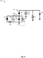
- FIG. 4 is a schematic diagram of a portion of receive circuitry 400 including a rectifier according to certain aspects of this disclosure.
- the receive circuitry 400 may correspond to a portion of the receiver 208.
- the receive circuitry 400 includes a receive antenna (e.g., inductor, coil, receiving element 352, etc.) 402.
- the receive circuitry 400 includes a coupling capacitor (C C ) 404, and a shunt resonant capacitor (C S ) 406 (e.g., 300 pF).
- C C 404 may be a large-value (e.g., 260 pF) capacitor and configured to couple AC power to the rectifier 420.
- the capacitors 404 and 406 may be provided to create a resonant structure at a desired resonant frequency.
- the receive circuitry 400 further includes a filter capacitor (C f ) 408 (e.g., .01 ⁇ F), which may be configured to filter/smooth the power transferred. Further, the equivalent resistance R L (e.g., 1 k ⁇ ) of the load (e.g., battery, implant device, etc.) powered by the receive circuitry 400 is shown. In certain aspects, the receive circuitry 400 includes an optional diode 410 (e.g., Zener diode) that is configured to act as a voltage clamp. Further, the parasitic resistance R P (e.g., 1 ⁇ ) of the capacitors and antenna is shown.
- a filter capacitor (C f ) 408 e.g., .01 ⁇ F
- R L e.g., 1 k ⁇
- the receive circuitry 400 includes an optional diode 410 (e.g., Zener diode) that is configured to act as a voltage clamp.
- the parasitic resistance R P e.g., 1 ⁇ )
- the rectifier 420 comprises a first diode 422 and a second diode 424 coupled in series. Further, the rectifier 420 includes a resistor (R S ) 426 (e.g., a high value resistor, such as, 100 k ⁇ ) coupled in parallel to the second diode 424, with a first terminal of the R S 426 being coupled to a first terminal of the second diode 424, and a second terminal of the R S 426 being coupled to a second terminal of the second diode 424.
- the first diode 422 and second diode 424 are configured to act as or part of a voltage doubler rectifier.
- Properties of rectifier 420 may be used as feedback information about the voltage level at the receive circuitry 400 (e.g., the voltage at the load connected to the receive circuitry 400). For example, as the power received by the antenna 402 from a wireless power transmitter (e.g., transmitter 204) rises, the nonlinear properties of the first diode 422 and the second diode 424 cause the first diode 422 and the second diode 424 to generate harmonics that change with voltage level.
- a wireless power transmitter e.g., transmitter 204
- a first threshold e.g., .5 V
- neither the first diode 422 nor the second diode 424 conducts as the R S 426 keeps the voltage at a node between the first diode 422 and the second diode 424 low. Accordingly, there is substantially no voltage at the load of the receive circuitry 400.
- the second diode 424 begins to conduct.
- the R S 426 in parallel with the second diode 424 causes the second diode 424 to conduct at power levels lower than the first diode 422.
- second harmonics of the received power signal e.g., received at a particular fundamental frequency
- second harmonics are based on the properties of the second diode 424 and not separately generated by active circuitry. Such second harmonics radiated back from the antenna 402 may be detectable by the wireless power transmitter (e.g., transmitter 204) as discussed further herein. At power levels where only the second diode 424 conducts, the voltage level at the load of the receive circuitry 400 may be below the desired voltage level.
- the first diode 422 begins to conduct in addition to the second diode 424.
- the influence of the R S 426 on the circuit becomes minimal as the voltage at the node between the first diode and the second diode 424 is set by the clamping action of the first diode 422 and the second diode 424.
- the first diode 422 and second diode 424 generate third harmonics of the received power signal. The third harmonics are radiated back through the antenna 402.
- third harmonics are based on the properties of the first diode 422 and the second diode 424 and not separately generated by active circuitry. Such third harmonics may be detectable by the wireless power transmitter (e.g., transmitter 204) as discussed further herein.
- the wireless power transmitter e.g., transmitter 204
- the voltage level at the load of the receive circuitry 400 may be at or near the desired voltage level.
- a wireless power transmitter e.g., transmitter 204
- the wireless power transmitter may utilize the level of each of or a ratio of the second and third harmonics to control the power of the charging field.
- the transmitter 204 may be configured to generate a clean (minimal second or third order harmonics) wireless field 205 to transmit to the receiver 208.
- the front-end circuit 226 may include a filter circuit configured to filter out second and third order harmonics from the signal utilized to generate the wireless field 205. Filtering out such second and third harmonics may help to prevent such second and third harmonics from the transmitter 204 being mistaken for second and third harmonics generated by the receiver 208.
- the transmitter 204 may receive the radiated harmonics from the receiver 208.
- the transmitter 204 may utilize the same power transmitting element 214 as used to generate the wireless field 205 to receive the radiated harmonics, or may use a different element (e.g., antenna, coil, etc.).
- the radiated harmonics may be received as part of a wireless field generated by the receiver 208, which may contain other signals, such as the wireless field 205.
- the transmitter 204 may control the power of the wireless field 205 emitted by the wireless power transmitter 204 based on the received harmonics as discussed herein.
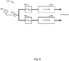
- FIG. 5 is a block diagram of a portion of transmit circuitry 500 according to certain aspects of this disclosure.
- the transmit circuitry 500 may correspond to a portion of the transmitter 204.
- the transmit circuitry 500 may be utilized to receive the radiated harmonics from the receiver 208.
- the transmitter circuitry 500 includes an antenna (e.g., power transmitting element 214, a separate antenna, coil, etc.) 502.
- the received signal from the antenna 502 may amplified by amplifier 503 and split and passed through two separate filters (e.g., band filters) that select for the second and third harmonics, respectively.
- the received signal may be passed through a first filter 504, as shown, which may comprise a band pass filter to pass frequencies in the signal corresponding to the second harmonics.
- the received signal may be passed through a second filter 506, as shown, which may comprise a band pass filter to pass frequencies in the signal corresponding to the third harmonics.
- each of the first filter 504 and the second filter 506 may then be sent to one or more signal processors (e.g., signal detectors) 508 to detect the relative strength of the second harmonics and third harmonics received.
- signal processors e.g., signal detectors
- separate signal processors 508 may be used to detect each of the second harmonics and third harmonics.
- a single signal processor 508 may be configured to detect both the second harmonics and third harmonics.
- Indications of the strength e.g., relative to one or more thresholds, absolute indicators, voltage output proportional to strength, etc.
- the signal processor 508 and the controller 240 may be implemented on a single chip or separate chips.
- the controller 240 may control the power of the wireless field 205 based on the indications of the strength of the second and third harmonics received from the receiver 208.
- the controller 240 in certain aspects, may be configured to incrementally increase the power of the wireless field 205 when initially powering a device (e.g., upon initial coupling between the transmitter 204 and receiver 208) until the strength of the received second harmonics is above a first threshold, and the strength of the received third harmonics is above a second threshold.
- the controller 240 may then hold the strength of the wireless field 205, or increase the strength of the wireless field 205 by a known quantity, until the receiver 208 is fully powered.
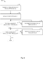
- FIG. 6 is a flowchart of example operations 600 for wireless power transfer, in accordance with certain aspects of the present disclosure.
- the transmitter 204 may generate a wireless field 205 at an initial power level (e.g., lowest power level) to transfer power to the receiver 208.
- the transmitter 204 may measure harmonic levels (e.g., second and third harmonics) at harmonics of the wireless field 205 to be generated.
- harmonic levels e.g., second and third harmonics
- the transmitter 204 may measure a received signal, which may include radiated harmonics from the receiver 208.
- the transmitter 204 may keep generating the wireless field 205 while measuring the radiated harmonics from the receiver 208. In certain aspects, the transmitter 204 may stop generating the wireless field 205 (e.g., by powering down the driver 224) temporarily while measuring the radiated harmonics from the receiver 208, and then return to generating the wireless field 205. At 615 the transmitter 204 determines if the second order harmonics in the received signal are above a first threshold. If the second order harmonics are not above the first threshold, at 620, the transmitter 204 increments the power level up of the wireless field 205 and returns to 615.
- the transmitter 204 determines if the third order harmonics on the received signal are above a second threshold. If the third order harmonics are not above the second threshold, at 630, the transmitter 204 increments the power level up of the wireless field 205 and returns to 625.
- the operations 600 may end.
- the transmitter 204 may hold the strength of the wireless field 205, or increase the strength of the wireless field 205 by a known quantity.
- the diodes of the receiver 208 are conducting and sufficient power is being received at the receiver 208 for the device with the receiver 208 to power up. Further control of the transmitter 204 and the receiver 208 may be achieved by other means and techniques for feedback.
- the receive circuitry 400 discussed with respect to FIG. 4 may be configured to generate harmonics using passive circuitry and not require any active circuitry (e.g., switches) to generate harmonics. Accordingly, the receive circuitry 400, as discussed, may not require additional power to control such active circuitry to generate harmonics and can work at very low power levels.
- receive circuitry at a receiver may be designed to have some active circuitry to selectively generate harmonics at the receiver 208 to communicate with the transmitter 204.
- the transmitter 204 may detect (e.g., utilizing the transmit circuitry 500) the harmonics generated by the receiver 208 and interpret the harmonics received as indicative of information communicated.
- the simple presence or not of harmonics can be indicative of a single bit of information (e.g., the receiver 208 has sufficient power or not, the receiver 208 is functioning normally or not, etc.).
- the harmonics may be modified (e.g., modulated or varied) to indicate additional information (e.g., bits of information corresponding to different modulation or variance).
- the harmonics may be modified by adjusting a passive diode rectification path, or other modification to rectification through components (e.g., switches, resistors, etc.) in the rectification path. For example, switching (e.g., by selectively opening and closing a switch) series resistance, load, topology changes, re-tuning of the resonator, etc. may all be performed to modify the harmonics created.
- the harmonics may be modified by modulating the harmonics by switching (e.g., by selectively opening and closing a switch) one or more switches of the active rectifier of the receiver 208.
- the harmonics may be modulated based on the power level of DC current produced by the active rectifier to signal to the transmitter 204 the power level at the receiver 208.
- the techniques described herein may utilize low power consumption techniques to selectively generate and/or modify the harmonics, so as to communicate information between the receiver 208 and the transmitter 204, while still being lower power than other active circuit techniques for communicating information.
- the harmonics generated by the receiver 208 may be even harmonics (e.g., 2 nd order, 4 th order, etc.) as opposed to odd harmonics to avoid a low signal to noise ratio at the transmitter 204 for receiving the harmonics from the receiver 208, as the transmitter 204 may also generate odd harmonics when generating the wireless field 205.
- the receiver 208 may utilize nonlinear components (e.g., a capacitor with capacitance as a function of voltage, such as a reverse biased diode junction (e.g., diode or FET)) to generate such even harmonics.
- FIG. 7 is a schematic diagram of a portion of receive circuitry 700 configured to selectively generate harmonics according to certain aspects of this disclosure.
- the receive circuitry 700 may correspond to a portion of the receiver 208.
- the receive circuitry 700 may have mostly the same components as the receive circuitry 400 of FIG. 4 , as shown.
- the receive circuitry 700 may further include a switch (e.g., transistor) 728 configured to selectively couple (by selectively opening and closing the switch 728) the resistor 726 in parallel with the second diode 724.
- the receive circuitry 700 may be configured to selectively generate harmonics (e.g., second and third harmonics) based on whether or not the resistor 726 is coupled in parallel with the second diode 724 or not.
- harmonics e.g., second and third harmonics
- harmonics may be generated when the resistor 726 is coupled in parallel with the second diode 724, and harmonics may not be generated when the resistor 726 is not coupled in parallel with the second diode 724.
- the switch 728 may be controlled by a controller, such as the controller 250.
- FIG. 8 is a schematic diagram of another portion of receive circuitry 800 configured to selectively generate harmonics according to certain aspects of this disclosure.
- the receive circuitry 800 may correspond to a portion of the receiver 208.
- the receive circuitry 800 may have mostly the same components as the receive circuitry 400 of FIG. 4 , as shown. However, the receive circuitry 800 may not include the resistor 426 of receive circuitry 400.
- the receive circuitry 800 may additionally include a capacitor 824 selectively coupled in parallel with the receive antenna 802.
- a switch (e.g., transistor) 828 may be coupled in series with the capacitor 824 and configured to selectively couple (by selectively opening and closing the switch 828) the capacitor 824 in parallel with the receive antenna 802.
- the receive circuitry 800 may additionally include an inductor 826 coupled in series with the antenna 802, wherein a coupling point of the capacitor 824 is between the receive antenna 802 and the inductor 826.
- the capacitor 824 and inductor 826 may be configured to act electromagnetic interference (EMI) filters that may block or pass harmonics from the receive circuitry 800.
- EMI electromagnetic interference
- selectively coupling or decoupling the capacitor 824 in parallel with the antenna 802 may disconnect or modify the effect as an EMI filter, and therefore block or pass harmonics.
- the inductor 826 and capacitor 824 may block harmonics from being generated.
- the receive circuitry 800 may generate harmonics.
- the switch 828 may be controlled by a controller, such as the controller 250.
- FIG. 9 is a schematic diagram of another portion of receive circuitry 900 configured to selectively generate harmonics according to certain aspects of this disclosure.
- the receive circuitry 900 may correspond to a portion of the receiver 208.
- the receive circuitry 900 may have mostly the same components as the receive circuitry 400 of FIG. 4 , as shown. However, the receive circuitry 900 may not include the resistor 426 of receive circuitry 400.
- the receive circuitry 900 may additionally include a capacitor 924 coupled in parallel with the receive antenna 902.
- a switch (e.g., transistor) 928 may be coupled in series with the capacitor 924 and configured to selectively couple (by selectively opening and closing the switch 928) the capacitor 924 in parallel with the receive antenna 902.
- the capacitor 924 may have a nonlinear capacitance (e.g., the capacitor 924 may be one of a transcap variable capacitor, varactor/diode, FET, etc.). Accordingly, if the capacitor 924 is coupled in parallel with the antenna 902, the receive circuitry 900 may generate even harmonics. However, if the capacitor 924 is not coupled in parallel with the antenna 902, the receive circuitry 900 may not generate harmonics.
- the switch 928 may be controlled by a controller, such as the controller 250.
- the capacitance of the capacitor 924 may be adjusted (e.g., the capacitor 924 may comprise a variable capacitor) to selectively generate harmonics.
- the capacitance of the capacitor 924 may be controlled by a controller, such as the controller 250.
- FIG. 10 is a schematic diagram of another portion of receive circuitry 1000 configured to selectively generate harmonics according to certain aspects of this disclosure.
- the receive circuitry 1000 may correspond to a portion of the receiver 208.
- the receive circuitry 1000 may have mostly the same components as the receive circuitry 400 of FIG. 4 , as shown.
- the receive circuitry 1000 may not include the resistor 426 of receive circuitry 400.
- the receive circuitry 1000 may not include the first diode 422 and second diode 424, which form a passive rectifier, but instead include an active rectifier, such as shown using transistors 1022 and 1024.
- the switch timing (opening and closing) of the transistors 1022 and 1024 can be modified to modulate harmonics, while still rectifying most of the received power from the transmitter 204.
- the transistors 1022 and 1024 may be selectively enabled and disabled to selectively enable and disable rectification. When rectification is enabled, harmonics may be generated. When rectification is disabled, harmonics may not be generated.
- the transistors 1022 and 1024 may be controlled by a controller, such as the controller 250.
- a transmitter 204 may be configured to receive such harmonics generated by any of the circuitry 700-1000 and perform an action (e.g., adjust a strength of the wireless field 205) based on the received harmonics.
- an action e.g., adjust a strength of the wireless field 205
- the controller 250 of the receiver 208 may be configured to selectively generate the harmonics to communicate to the transmitter 204 information that the transmitter 204 may utilize to perform an action.
- the various operations of methods described above may be performed by any suitable means capable of performing the corresponding functions.
- the means may include various hardware and/or software component(s) and/or module(s), including, but not limited to a circuit, an application-specific integrated circuit (ASIC), or processor.
- ASIC application-specific integrated circuit
- determining encompasses a wide variety of actions. For example, “determining” may include calculating, computing, processing, deriving, investigating, looking up (e.g., looking up in a table, a database, or another data structure), ascertaining, and the like. Also, “determining” may include receiving (e.g., receiving information), accessing (e.g., accessing data in a memory), and the like. Also, “determining” may include resolving, selecting, choosing, establishing, and the like.
- a phrase referring to "at least one of' a list of items refers to any combination of those items, including single members.
- "at least one of: a, b, or c" is intended to cover: a, b, c, a-b, a-c, b-c, and a-b-c, as well as any combination with multiples of the same element (e.g., a-a, a-a-a, a-a-b, a-a-c, a-b-b, a-c-c, b-b, b-b-b, b-b-c, c-c, and c-c-c or any other ordering of a, b, and c ) .
- DSP digital signal processor
- ASIC application specific integrated circuit
- FPGA field programmable gate array
- PLD programmable logic device
- a general-purpose processor may be a microprocessor, but in the alternative, the processor may be any commercially available processor, controller, microcontroller, or state machine.
- a processor may also be implemented as a combination of computing devices, e.g., a combination of a DSP and a microprocessor, a plurality of microprocessors, one or more microprocessors in conjunction with a DSP core, or any other such configuration.
- the methods disclosed herein comprise one or more steps or actions for achieving the described method.
- the method steps and/or actions may be interchanged with one another. In other words, unless a specific order of steps or actions is specified, the order and/or use of specific steps and/or actions may be modified.
- an example hardware configuration may comprise a processing system in a wireless node.
- the processing system may be implemented with a bus architecture.
- the bus may include any number of interconnecting buses and bridges depending on the specific application of the processing system and the overall design constraints.
- the bus may link together various circuits including a processor, machine-readable media, and a bus interface.
- the bus interface may be used to connect a network adapter, among other things, to the processing system via the bus.
- the network adapter may be used to implement the signal processing functions of the physical (PHY) layer.
- a user interface e.g., keypad, display, mouse, joystick, etc.
- the bus may also link various other circuits such as timing sources, peripherals, voltage regulators, power management circuits, and the like, which are well known in the art, and therefore, will not be described any further.
- the processing system may be configured as a general-purpose processing system with one or more microprocessors providing the processor functionality and external memory providing at least a portion of the machine-readable media, all linked together with other supporting circuitry through an external bus architecture.
- the processing system may be implemented with an ASIC with the processor, the bus interface, the user interface in the case of an access terminal), supporting circuitry, and at least a portion of the machine-readable media integrated into a single chip, or with one or more FPGAs, PLDs, controllers, state machines, gated logic, discrete hardware components, or any other suitable circuitry, or any combination of circuits that can perform the various functionality described throughout this disclosure.
Description
- The present Application for Patent claims benefit of and priority to
U.S. Patent Application No. 15/241,394, filed August 19, 2016 - The present disclosure relates to a wireless power receiver, a wireless power transmitter and a method for controlling a wireless power transmitter.
- An increasing number and variety of electronic devices are powered via rechargeable batteries. Such devices include mobile phones, portable music players, laptop computers, tablet computers, computer peripheral devices, communication devices (e.g., Bluetooth devices), digital cameras, hearing aids, medical implants, and the like. While battery technology has improved, battery-powered electronic devices increasingly require and consume greater amounts of power. As such, these devices constantly require recharging. Rechargeable devices are often charged via wired connections that require cables or other similar connectors that are physically connected to a power supply. Cables and similar connectors may sometimes be inconvenient or cumbersome and have other drawbacks. Wireless power transfer systems, for example, may allow users to charge and/or power electronic devices without physical, electrical connections, thus reducing the number of components required for operation of the electronic devices and simplifying the use of the electronic device.
- For example, some battery powered devices, such as medical implants (e.g., pacemakers, neuromodulation devices, insulin pumps, etc.) may be located/positioned in areas where replacing the battery is not always feasible (e.g., in a body, such as, a human body). For example, to change a battery for a medical implant, surgery may need to be performed, which is risky. Accordingly, it may be safer to charge such devices wirelessly.
- Further, some electronic devices may not be battery powered, but it still may be beneficial to utilize wireless power transfer to power such devices. In particular, the use of wireless power may eliminate the need for cords/cables to be attached to the electronic devices, which may be inconvenient and aesthetically displeasing.
- Different electronic devices may have different shapes, sizes, and power requirements. There is flexibility in having different sizes and shapes in the components (e.g., magnetic coil, charging plate, etc.) that make up a wireless power transmitter and/or a wireless power receiver in terms of industrial design and support for a wide range of devices.
WO2015/071902 describes a system and method for selecting power transmitters across a wireless power coupling.
US2015/349538 describes an active rectifier for efficient wireless power transfer. - According to a first aspect of the present disclosure, a wireless power receiver is provided as defined by the features of independent claim 1.
- According to a second aspect of the present disclosure, a wireless power transmitter is provided as defined by the features of independent claim 8.
- According to a third aspect of the present disclosure, there is provided a method for controlling a wireless power transmitter. The method includes generating a wireless field for wireless power transfer at a power level. The method further includes detecting levels of second harmonics and third harmonics of the generated wireless field. The method further includes incrementally increasing the power level of the wireless field based on detecting levels of second harmonics above a first threshold. The method further includes holding the power level of the wireless field based on detecting levels of second harmonics above the first threshold and levels of third harmonics above a second threshold.
- The following detailed description and accompanying drawings provide a better understanding of the nature and advantages of the present disclosure.
- With respect to the discussion to follow and in particular to the drawings, it is stressed that the particulars shown represent examples for purposes of illustrative discussion, and are presented in the cause of providing a description of principles and conceptual aspects of the present disclosure. In this regard, no attempt is made to show implementation details beyond what is needed for a fundamental understanding of the present disclosure. The discussion to follow, in conjunction with the drawings, makes apparent to those of skill in the art how embodiments in accordance with the present disclosure may be practiced. In the accompanying drawings:
-
FIG. 1 is a functional block diagram of a wireless power transfer system in accordance with an illustrative aspect. -
FIG. 2 is a functional block diagram of a wireless power transfer system in accordance with an illustrative aspect. -
FIG. 3 is a schematic diagram of a portion of transmit circuitry or receive circuitry ofFIG. 2 including a power transmitting or receiving element in accordance with an illustrative aspect. -
FIG. 4 is a schematic diagram of a portion of receive circuitry including a rectifier according to certain aspects of this disclosure. -
FIG. 5 is a block diagram of a portion of transmit circuitry according to certain aspects of this disclosure. -
FIG. 6 is a flowchart of example operations for wireless power transfer, in accordance with certain aspects of the present disclosure. -
FIG. 7 is a schematic diagram of a portion of receive circuitry configured to selectively generate harmonics according to certain aspects of this disclosure. -
FIG. 8 is a schematic diagram of a portion of receive circuitry configured to selectively generate harmonics according to certain aspects of this disclosure. -
FIG. 9 is a schematic diagram of a portion of receive circuitry configured to selectively generate harmonics according to certain aspects of this disclosure. -
FIG. 10 is a schematic diagram of a portion of receive circuitry configured to selectively generate harmonics according to certain aspects of this disclosure. - Drawing elements that are common among the following figures may be identified using the same reference numerals.
- Wireless power transfer may refer to transferring any form of energy associated with electric fields, magnetic fields, electromagnetic fields, or otherwise from a transmitter to a receiver without the use of physical electrical conductors (e.g., power may be transferred through free space). The power output into a wireless field (e.g., a magnetic field or an electromagnetic field) may be received, captured by, or coupled by a "power receiving element" to achieve power transfer.
-
FIG. 1 is a functional block diagram of a wirelesspower transfer system 100, in accordance with an illustrative aspect.Input power 102 may be provided to atransmitter 104 from a power source (not shown in this figure) to generate a wireless (e.g., magnetic or electromagnetic)field 105 for performing energy transfer. Areceiver 108 may couple to thewireless field 105 and generateoutput power 110 for storing or consumption by a device (not shown in this figure) coupled to theoutput power 110. Thetransmitter 104 and thereceiver 108 may be separated by adistance 112. Thetransmitter 104 may include a power transmittingelement 114 for transmitting/coupling energy to thereceiver 108. Thereceiver 108 may include a power receivingelement 118 for receiving or capturing/coupling energy transmitted from thetransmitter 104. - In one illustrative aspect, the
transmitter 104 and thereceiver 108 may be configured according to a mutual resonant relationship. When the resonant frequency of thereceiver 108 and the resonant frequency of thetransmitter 104 are substantially the same or very close, transmission losses between thetransmitter 104 and thereceiver 108 are reduced. As such, wireless power transfer may be provided over larger distances. Resonant inductive coupling techniques may thus allow for improved efficiency and power transfer over various distances and with a variety of inductive power transmitting and receiving element configurations. - In certain aspects, the
wireless field 105 may correspond to the "near field" of thetransmitter 104. The near-field may correspond to a region in which there are strong reactive fields resulting from the currents and charges in the power transmittingelement 114 that minimally radiate power away from the power transmittingelement 114. The near-field may correspond to a region that is within about one wavelength (or a fraction thereof) of the power transmittingelement 114. Conversely, the far field may correspond to a region that is greater than about one wavelength of the power transmittingelement 114. - In certain aspects, efficient energy transfer may occur by coupling a large portion of the energy in the
wireless field 105 to the power receivingelement 118 rather than propagating most of the energy in an electromagnetic wave to the far field. - In certain implementations, the
transmitter 104 may output a time varying magnetic (or electromagnetic) field with a frequency corresponding to the resonant frequency of the power transmittingelement 114. When thereceiver 108 is within thewireless field 105, the time varying magnetic (or electromagnetic) field may induce a current in thepower receiving element 118. As described above, if thepower receiving element 118 is configured as a resonant circuit to resonate at the frequency of thepower transmitting element 114, energy may be efficiently transferred. An alternating current (AC) signal induced in thepower receiving element 118 may be rectified to produce a direct current (DC) signal that may be provided to charge or to power a load. -
FIG. 2 is a functional block diagram of a wirelesspower transfer system 200, in accordance with another illustrative aspect. Thesystem 200 may include atransmitter 204 and areceiver 208. The transmitter 204 (also referred to herein as power transfer unit, PTU) may include transmitcircuitry 206 that may include anoscillator 222, adriver circuit 224, and a front-end circuit 226. Theoscillator 222 may be configured to generate an oscillator signal (also known as an oscillating signal) at a desired frequency (e.g., fundamental frequency) that may adjust in response to afrequency control signal 223. Theoscillator 222 may provide the oscillator signal to thedriver circuit 224. Thedriver circuit 224 may be configured to drive thepower transmitting element 214 at, for example, a resonant frequency of thepower transmitting element 214 based on an input voltage signal (VD) 225. Thedriver circuit 224 may be a switching amplifier configured to receive a square wave from theoscillator 222 and output as a driving signal output a sine wave. - The front-
end circuit 226 may include a filter circuit configured to filter out harmonics or other unwanted frequencies. The front-end circuit 226 may include a matching circuit configured to match the impedance of thetransmitter 204 to the impedance of thepower transmitting element 214. As will be explained in more detail below, the front-end circuit 226 may include a tuning circuit to create a resonant circuit with thepower transmitting element 214. As a result of driving thepower transmitting element 214, thepower transmitting element 214 may generate awireless field 205 to wirelessly output power at a level sufficient for charging abattery 236, or otherwise powering a load. - The
transmitter 204 may further include acontroller 240 operably coupled to the transmitcircuitry 206 and configured to control one or more aspects of the transmitcircuitry 206, or accomplish other operations relevant to managing the transfer of power. Thecontroller 240 may be a micro-controller or a processor. Thecontroller 240 may be implemented as an application-specific integrated circuit (ASIC). Thecontroller 240 may be operably connected, directly or indirectly, to each component of the transmitcircuitry 206. Thecontroller 240 may be further configured to receive information from each of the components of the transmitcircuitry 206 and perform calculations based on the received information. Thecontroller 240 may be configured to generate control signals (e.g., signal 223) for each of the components that may adjust the operation of that component. As such, thecontroller 240 may be configured to adjust or manage the power transfer based on a result of the operations performed by it. Thetransmitter 204 may further include a memory (not shown) configured to store data, for example, such as instructions for causing thecontroller 240 to perform particular functions, such as those related to management of wireless power transfer. - The receiver 208 (also referred to herein as power receiving unit, PRU) may include receive
circuitry 210 that may include a front-end circuit 232 and arectifier circuit 234. The front-end circuit 232 may include matching circuitry configured to match the impedance of the receivecircuitry 210 to the impedance of thepower receiving element 218. As will be explained below, the front-end circuit 232 may further include a tuning circuit to create a resonant circuit with thepower receiving element 218. Therectifier circuit 234 may generate a DC power output from an AC power input to charge thebattery 236, as shown inFIG. 2 . Thereceiver 208 and thetransmitter 204 may additionally communicate on a separate communication channel 219 (e.g., Bluetooth, Zigbee, cellular, etc.). Thereceiver 208 and thetransmitter 204 may alternatively communicate via in-band signaling using characteristics of thewireless field 205. - The
receiver 208 may be configured to determine whether an amount of power transmitted by thetransmitter 204 and received by thereceiver 208 is appropriate for charging thebattery 236. In certain aspects, thetransmitter 204 may be configured to generate a predominantly non-radiative field with a direct field coupling coefficient (k) for providing energy transfer.Receiver 208 may directly couple to thewireless field 205 and may generate an output power for storing or consumption by a battery (or load) 236 coupled to the output or receivecircuitry 210. - The
receiver 208 may further include acontroller 250 configured similarly to the transmitcontroller 240 as described above for managing one or more aspects of thewireless power receiver 208. Thereceiver 208 may further include a memory (not shown) configured to store data, for example, such as instructions for causing thecontroller 250 to perform particular functions, such as those related to management of wireless power transfer. - As discussed above,
transmitter 204 andreceiver 208 may be separated by a distance and may be configured according to a mutual resonant relationship to minimize transmission losses between thetransmitter 204 and thereceiver 208. -
FIG. 3 is a schematic diagram of a portion of the transmitcircuitry 206 or the receivecircuitry 210 ofFIG. 2 , in accordance with illustrative aspects. As illustrated inFIG. 3 , transmit or receivecircuitry 350 may include a power transmitting or receivingelement 352 and atuning circuit 360. The power transmitting or receivingelement 352 may also be referred to or be configured as an antenna or a "loop" antenna. The term "antenna" generally refers to a component that may wirelessly output or receive energy for coupling to another antenna. The power transmitting or receivingelement 352 may also be referred to herein or be configured as a "magnetic" antenna, or an induction coil, a resonator, or a portion of a resonator. The power transmitting or receivingelement 352 may also be referred to as a coil or resonator of a type that is configured to wirelessly output or receive power. As used herein, the power transmitting or receivingelement 352 is an example of a "power transfer component" of a type that is configured to wirelessly output and/or receive power. The power transmitting or receivingelement 352 may include an air core or a physical core such as a ferrite core (not shown in this figure). - When the power transmitting or receiving
element 352 is configured as a resonant circuit or resonator withtuning circuit 360, the resonant frequency of the power transmitting or receivingelement 352 may be based on the inductance and capacitance. Inductance may be simply the inductance created by a coil and/or other inductor forming the power transmitting or receivingelement 352. Capacitance (e.g., a capacitor) may be provided by thetuning circuit 360 to create a resonant structure at a desired resonant frequency. As a non limiting example, thetuning circuit 360 may comprise acapacitor 354 and acapacitor 356, which may be added to the transmit and/or receivecircuitry 350 to create a resonant circuit. - The
tuning circuit 360 may include other components to form a resonant circuit with the power transmitting or receivingelement 352. As another non limiting example, thetuning circuit 360 may include a capacitor (not shown) placed in parallel between the two terminals of thecircuitry 350. Still other designs are possible. In some aspects, the tuning circuit in the front-end circuit 226 may have the same design (e.g., 360) as the tuning circuit in front-end circuit 232. In other aspects, the front-end circuit 226 may use a tuning circuit design different than in the front-end circuit 232. - For power transmitting elements, the
signal 358, with a frequency that substantially corresponds to the resonant frequency of the power transmitting or receivingelement 352, may be an input to the power transmitting or receivingelement 352. For power receiving elements, thesignal 358, with a frequency that substantially corresponds to the resonant frequency of the power transmitting or receivingelement 352, may be an output from the power transmitting or receivingelement 352. Although aspects disclosed herein may be generally directed to resonant wireless power transfer, persons of ordinary skill will appreciate that aspects disclosed herein may be used in non-resonant implementations for wireless power transfer. - In some aspects, when power (e.g., energy) is wirelessly received by a device (e.g., medical implant) with a wireless power receiver (e.g., receiver 208) from a wireless power transmitter (e.g., transmitter 204), there may be a method of power control to ensure that the correct amount of power is transferred from the
transmitter 204 to thereceiver 208. For example, the device with thereceiver 208 may be configured to operate/charge at a particular voltage (e.g., 4.2 V). However, generating a fixedstrength wireless field 205 by thetransmitter 204 may not produce the desired voltage at thereceiver 208. For example, the amount of power transferred between thetransmitter 204 and thereceiver 208 at any given strength of thewireless field 205 may differ based on the distance between (and/or other factors such as materials between, etc.) thetransmitter 204 and thereceiver 208. Accordingly, the power (e.g., voltage) generated by thereceiver 208 for the device may be variable based on one or more factors for the same strength ofwireless field 205 from thetransmitter 204. For example, a medical implant device may be implanted in a person at various distances/positions under the skin and with varying tissue types and thicknesses. Accordingly, certain aspects discussed herein relate to systems and methods for controlling the power transferred from a wireless power transmitter to a wireless power receiver to ensure that the device with the wireless power receiver receives the correct power supply. - In some aspects, a closed-loop power control scheme may be employed to adjust the strength of the
wireless field 205 to ensure that the power (e.g., voltage) at the device being wirelessly powered is the desired power (e.g., desired voltage). For example, in some aspects, thewireless receiver 208 may be configured to actively determine a power level of the power received at thereceiver 208, such as, a voltage at therectifier 234. For example, thecontroller 250 may be configured to monitor the voltage at therectifier 234. Depending on whether the voltage at therectifier 234 is above or below a range of the desired voltage level, the wireless receiver 208 (e.g., as controlled by the controller 250) may transmit feedback information (e.g., as a control signal) (e.g., viacommunication channel 219 or in-band signaling using the wireless field 205) to thewireless transmitter 204 indicating whether a strength of thewireless field 205 should be increased or decreased. No control signal may be sent if the voltage at therectifier 234 is within the range of the desired voltage level. Thewireless transmitter 204 may receive the control signal and adjust the strength of the wireless field 205 (e.g., by control from the controller 240), accordingly. - In some aspects, the power levels at the
receiver 208 may be very low, and therefore higher power techniques for transmitting feedback information (e.g., higher power communication viacommunication channel 219 or in-band signaling) may not be feasible. In particular, the device with thereceiver 208 may not be able to actively transmit feedback information to thetransmitter 204, so thetransmitter 204 does not have information about the voltage at the device being charged and cannot adjust the strength of thewireless field 205 to ensure the device is operating at the correct voltage using current techniques. For example, if a battery at the device is fully discharged, there may be a delay in time (e.g., 10 s) between when power is initially received by thewireless receiver 208 at the device from thewireless power transmitter 204 and when the device boots up and is able to use the communication channel 219 (e.g., via a radio) or in-band signaling (e.g., as controlled by thecontroller 250, which requires power), to transmit the feedback information to thetransmitter 204. In some cases, the device may not have means (e.g., a radio) to transmit the feedback information. - Accordingly, certain aspects of the present disclosure are directed to feedback mechanisms for wireless power transfer in order to control a power level of the wireless power transmitter. In particular, as discussed,
receiver 208 includes arectifier 234 to generate a DC power output from an AC power input. Certain aspects of the present disclosure are directed to a rectifier designed to provide feedback information about the voltage level at thereceiver 208. In particular, certain aspects are directed to areceiver 208 configured to generate harmonics during rectification and use such harmonics to communicate with thetransmitter 204. For example, thereceiver 208 may generate certain harmonics that indicate there is enough power at thereceiver 208, or even any other information (e.g., other status information of the receiver 208). In certain aspects, thetransmitter 204 may detect such harmonics (e.g., via an antenna, such as, transmitting element 214). In certain aspects, the detection of harmonics may indicate to thetransmitter 204 that a device (e.g., receiver 208) configured and able to receive wireless power is present and absorbing wireless power. In certain aspects, the detection of harmonics may indicate other information as discussed. -
FIG. 4 is a schematic diagram of a portion of receivecircuitry 400 including a rectifier according to certain aspects of this disclosure. The receivecircuitry 400 may correspond to a portion of thereceiver 208. As shown the receivecircuitry 400 includes a receive antenna (e.g., inductor, coil, receivingelement 352, etc.) 402. Further, the receivecircuitry 400 includes a coupling capacitor (CC) 404, and a shunt resonant capacitor (CS) 406 (e.g., 300 pF).C C 404 may be a large-value (e.g., 260 pF) capacitor and configured to couple AC power to therectifier 420. Thecapacitors - The receive
circuitry 400 further includes a filter capacitor (Cf) 408 (e.g., .01 µF), which may be configured to filter/smooth the power transferred. Further, the equivalent resistance RL (e.g., 1 kΩ) of the load (e.g., battery, implant device, etc.) powered by the receivecircuitry 400 is shown. In certain aspects, the receivecircuitry 400 includes an optional diode 410 (e.g., Zener diode) that is configured to act as a voltage clamp. Further, the parasitic resistance RP (e.g., 1 Ω) of the capacitors and antenna is shown. - The
rectifier 420 comprises afirst diode 422 and asecond diode 424 coupled in series. Further, therectifier 420 includes a resistor (RS) 426 (e.g., a high value resistor, such as, 100 kΩ) coupled in parallel to thesecond diode 424, with a first terminal of theR S 426 being coupled to a first terminal of thesecond diode 424, and a second terminal of theR S 426 being coupled to a second terminal of thesecond diode 424. In certain aspects, thefirst diode 422 andsecond diode 424 are configured to act as or part of a voltage doubler rectifier. - Properties of
rectifier 420, may be used as feedback information about the voltage level at the receive circuitry 400 (e.g., the voltage at the load connected to the receive circuitry 400). For example, as the power received by theantenna 402 from a wireless power transmitter (e.g., transmitter 204) rises, the nonlinear properties of thefirst diode 422 and thesecond diode 424 cause thefirst diode 422 and thesecond diode 424 to generate harmonics that change with voltage level. At power levels received by theantenna 402 below a first threshold (e.g., .5 V) neither thefirst diode 422 nor thesecond diode 424 conducts as theR S 426 keeps the voltage at a node between thefirst diode 422 and thesecond diode 424 low. Accordingly, there is substantially no voltage at the load of the receivecircuitry 400. - As the power received by the
antenna 402 from a wireless power transmitter (e.g., transmitter 204) rises above the first threshold, but below a second threshold (e.g., .5 V above the voltage on RL), thesecond diode 424 begins to conduct. In particular, theR S 426 in parallel with thesecond diode 424 causes thesecond diode 424 to conduct at power levels lower than thefirst diode 422. As thesecond diode 424 conducts, second harmonics of the received power signal (e.g., received at a particular fundamental frequency) are generated by thesecond diode 424 and radiated back through theantenna 402. It should be noted that such generation of second harmonics is based on the properties of thesecond diode 424 and not separately generated by active circuitry. Such second harmonics radiated back from theantenna 402 may be detectable by the wireless power transmitter (e.g., transmitter 204) as discussed further herein. At power levels where only thesecond diode 424 conducts, the voltage level at the load of the receivecircuitry 400 may be below the desired voltage level. - Further, as the power received by the
antenna 402 from a wireless power transmitter (e.g., transmitter 204) rises above the second threshold, thefirst diode 422 begins to conduct in addition to thesecond diode 424. In particular, at these higher power levels, the influence of theR S 426 on the circuit becomes minimal as the voltage at the node between the first diode and thesecond diode 424 is set by the clamping action of thefirst diode 422 and thesecond diode 424. Thefirst diode 422 andsecond diode 424 generate third harmonics of the received power signal. The third harmonics are radiated back through theantenna 402. It should be noted that such generation of third harmonics is based on the properties of thefirst diode 422 and thesecond diode 424 and not separately generated by active circuitry. Such third harmonics may be detectable by the wireless power transmitter (e.g., transmitter 204) as discussed further herein. At power levels where thefirst diode 422 and thesecond diode 424 conduct, the voltage level at the load of the receivecircuitry 400 may be at or near the desired voltage level. - A wireless power transmitter, e.g.,
transmitter 204, may be configured to detect the second and third harmonics radiated (e.g., reflected) from theantenna 402, and based on those signals control the power of the charging field emitted by the wireless power transmitter. In certain aspects, the wireless power transmitter may utilize the level of each of or a ratio of the second and third harmonics to control the power of the charging field. - In certain aspects, the
transmitter 204 may be configured to generate a clean (minimal second or third order harmonics)wireless field 205 to transmit to thereceiver 208. For example, the front-end circuit 226 may include a filter circuit configured to filter out second and third order harmonics from the signal utilized to generate thewireless field 205. Filtering out such second and third harmonics may help to prevent such second and third harmonics from thetransmitter 204 being mistaken for second and third harmonics generated by thereceiver 208. As the power level of thewireless field 205 increases, and thefirst diode 422 and/or thesecond diode 424 begin conducting, thetransmitter 204 may receive the radiated harmonics from thereceiver 208. Thetransmitter 204 may utilize the samepower transmitting element 214 as used to generate thewireless field 205 to receive the radiated harmonics, or may use a different element (e.g., antenna, coil, etc.). The radiated harmonics may be received as part of a wireless field generated by thereceiver 208, which may contain other signals, such as thewireless field 205. Thetransmitter 204 may control the power of thewireless field 205 emitted by thewireless power transmitter 204 based on the received harmonics as discussed herein. -
FIG. 5 is a block diagram of a portion of transmitcircuitry 500 according to certain aspects of this disclosure. The transmitcircuitry 500 may correspond to a portion of thetransmitter 204. The transmitcircuitry 500 may be utilized to receive the radiated harmonics from thereceiver 208. As shown thetransmitter circuitry 500 includes an antenna (e.g.,power transmitting element 214, a separate antenna, coil, etc.) 502. The received signal from theantenna 502 may amplified byamplifier 503 and split and passed through two separate filters (e.g., band filters) that select for the second and third harmonics, respectively. In particular, the received signal may be passed through afirst filter 504, as shown, which may comprise a band pass filter to pass frequencies in the signal corresponding to the second harmonics. In addition, the received signal may be passed through asecond filter 506, as shown, which may comprise a band pass filter to pass frequencies in the signal corresponding to the third harmonics. - The output of each of the
first filter 504 and thesecond filter 506 may then be sent to one or more signal processors (e.g., signal detectors) 508 to detect the relative strength of the second harmonics and third harmonics received. In certain aspects,separate signal processors 508 may be used to detect each of the second harmonics and third harmonics. In certain aspects, asingle signal processor 508 may be configured to detect both the second harmonics and third harmonics. Indications of the strength (e.g., relative to one or more thresholds, absolute indicators, voltage output proportional to strength, etc.) may be sent from thesignal processor 508 to the controller 240 (or another processor) to adjust the power of thewireless field 205. In certain aspects, thesignal processor 508 and thecontroller 240 may be implemented on a single chip or separate chips. - The
controller 240 may control the power of thewireless field 205 based on the indications of the strength of the second and third harmonics received from thereceiver 208. In particular, thecontroller 240, in certain aspects, may be configured to incrementally increase the power of thewireless field 205 when initially powering a device (e.g., upon initial coupling between thetransmitter 204 and receiver 208) until the strength of the received second harmonics is above a first threshold, and the strength of the received third harmonics is above a second threshold. Thecontroller 240 may then hold the strength of thewireless field 205, or increase the strength of thewireless field 205 by a known quantity, until thereceiver 208 is fully powered. -
FIG. 6 is a flowchart ofexample operations 600 for wireless power transfer, in accordance with certain aspects of the present disclosure. - At 605, the
transmitter 204 may generate awireless field 205 at an initial power level (e.g., lowest power level) to transfer power to thereceiver 208. In certain aspects, before generating thewireless field 205, thetransmitter 204 may measure harmonic levels (e.g., second and third harmonics) at harmonics of thewireless field 205 to be generated. In some aspects, thresholds for the second harmonics and third harmonics for detection of a wireless power receiver, adjustment of the power level of thewireless field 205, etc., may be adjusted based on the measured harmonic levels (e.g., use the measured harmonics levels as a baseline and look for an increase by a certain threshold). At 610, thetransmitter 204 may measure a received signal, which may include radiated harmonics from thereceiver 208. In certain aspects, thetransmitter 204 may keep generating thewireless field 205 while measuring the radiated harmonics from thereceiver 208. In certain aspects, thetransmitter 204 may stop generating the wireless field 205 (e.g., by powering down the driver 224) temporarily while measuring the radiated harmonics from thereceiver 208, and then return to generating thewireless field 205. At 615 thetransmitter 204 determines if the second order harmonics in the received signal are above a first threshold. If the second order harmonics are not above the first threshold, at 620, thetransmitter 204 increments the power level up of thewireless field 205 and returns to 615. - If the second order harmonics are above the first threshold, at 625, the
transmitter 204 determines if the third order harmonics on the received signal are above a second threshold. If the third order harmonics are not above the second threshold, at 630, thetransmitter 204 increments the power level up of thewireless field 205 and returns to 625. - If the third order harmonics are above the second threshold, the
operations 600 may end. Thetransmitter 204 may hold the strength of thewireless field 205, or increase the strength of thewireless field 205 by a known quantity. In particular, once the third order harmonics are above the second threshold, the diodes of thereceiver 208 are conducting and sufficient power is being received at thereceiver 208 for the device with thereceiver 208 to power up. Further control of thetransmitter 204 and thereceiver 208 may be achieved by other means and techniques for feedback. - In some aspects, the receive
circuitry 400 discussed with respect toFIG. 4 may be configured to generate harmonics using passive circuitry and not require any active circuitry (e.g., switches) to generate harmonics. Accordingly, the receivecircuitry 400, as discussed, may not require additional power to control such active circuitry to generate harmonics and can work at very low power levels. - In some other aspects, receive circuitry at a receiver (e.g., receiver 208) may be designed to have some active circuitry to selectively generate harmonics at the
receiver 208 to communicate with thetransmitter 204. Thetransmitter 204 may detect (e.g., utilizing the transmit circuitry 500) the harmonics generated by thereceiver 208 and interpret the harmonics received as indicative of information communicated. In particular, by utilizing some active circuitry, when and how the harmonics are generated can be actively controlled by thereceiver 208, so almost any information can be indicated by such harmonics. For example, in some aspects, the simple presence or not of harmonics can be indicative of a single bit of information (e.g., thereceiver 208 has sufficient power or not, thereceiver 208 is functioning normally or not, etc.). Further. In some aspects, the harmonics may be modified (e.g., modulated or varied) to indicate additional information (e.g., bits of information corresponding to different modulation or variance). For example, in some aspects the harmonics may be modified by adjusting a passive diode rectification path, or other modification to rectification through components (e.g., switches, resistors, etc.) in the rectification path. For example, switching (e.g., by selectively opening and closing a switch) series resistance, load, topology changes, re-tuning of the resonator, etc. may all be performed to modify the harmonics created. In some aspects, the harmonics may be modified by modulating the harmonics by switching (e.g., by selectively opening and closing a switch) one or more switches of the active rectifier of thereceiver 208. The harmonics may be modulated based on the power level of DC current produced by the active rectifier to signal to thetransmitter 204 the power level at thereceiver 208. The techniques described herein, in some aspects, may utilize low power consumption techniques to selectively generate and/or modify the harmonics, so as to communicate information between thereceiver 208 and thetransmitter 204, while still being lower power than other active circuit techniques for communicating information. - In some aspects, the harmonics generated by the
receiver 208 may be even harmonics (e.g., 2nd order, 4th order, etc.) as opposed to odd harmonics to avoid a low signal to noise ratio at thetransmitter 204 for receiving the harmonics from thereceiver 208, as thetransmitter 204 may also generate odd harmonics when generating thewireless field 205. Accordingly, in certain aspects, thereceiver 208 may utilize nonlinear components (e.g., a capacitor with capacitance as a function of voltage, such as a reverse biased diode junction (e.g., diode or FET)) to generate such even harmonics. -
FIG. 7 is a schematic diagram of a portion of receivecircuitry 700 configured to selectively generate harmonics according to certain aspects of this disclosure. The receivecircuitry 700 may correspond to a portion of thereceiver 208. In particular, the receivecircuitry 700 may have mostly the same components as the receivecircuitry 400 ofFIG. 4 , as shown. However, the receivecircuitry 700 may further include a switch (e.g., transistor) 728 configured to selectively couple (by selectively opening and closing the switch 728) theresistor 726 in parallel with thesecond diode 724. Accordingly, the receivecircuitry 700 may be configured to selectively generate harmonics (e.g., second and third harmonics) based on whether or not theresistor 726 is coupled in parallel with thesecond diode 724 or not. For example, in some aspects, harmonics may be generated when theresistor 726 is coupled in parallel with thesecond diode 724, and harmonics may not be generated when theresistor 726 is not coupled in parallel with thesecond diode 724. Theswitch 728 may be controlled by a controller, such as thecontroller 250. -
FIG. 8 is a schematic diagram of another portion of receivecircuitry 800 configured to selectively generate harmonics according to certain aspects of this disclosure. The receivecircuitry 800 may correspond to a portion of thereceiver 208. In particular, the receivecircuitry 800 may have mostly the same components as the receivecircuitry 400 ofFIG. 4 , as shown. However, the receivecircuitry 800 may not include theresistor 426 of receivecircuitry 400. Further, the receivecircuitry 800 may additionally include a capacitor 824 selectively coupled in parallel with the receiveantenna 802. In particular, a switch (e.g., transistor) 828 may be coupled in series with the capacitor 824 and configured to selectively couple (by selectively opening and closing the switch 828) the capacitor 824 in parallel with the receiveantenna 802. Further, the receivecircuitry 800 may additionally include aninductor 826 coupled in series with theantenna 802, wherein a coupling point of the capacitor 824 is between the receiveantenna 802 and theinductor 826. The capacitor 824 andinductor 826 may be configured to act electromagnetic interference (EMI) filters that may block or pass harmonics from the receivecircuitry 800. In particular, selectively coupling or decoupling the capacitor 824 in parallel with theantenna 802 may disconnect or modify the effect as an EMI filter, and therefore block or pass harmonics. For example, if the capacitor 824 is coupled in parallel with theantenna 802, theinductor 826 and capacitor 824 may block harmonics from being generated. However, if the capacitor 824 is not coupled in parallel with theantenna 802, the receivecircuitry 800 may generate harmonics. Theswitch 828 may be controlled by a controller, such as thecontroller 250. -
FIG. 9 is a schematic diagram of another portion of receivecircuitry 900 configured to selectively generate harmonics according to certain aspects of this disclosure. The receivecircuitry 900 may correspond to a portion of thereceiver 208. In particular, the receivecircuitry 900 may have mostly the same components as the receivecircuitry 400 ofFIG. 4 , as shown. However, the receivecircuitry 900 may not include theresistor 426 of receivecircuitry 400. Further, the receivecircuitry 900 may additionally include acapacitor 924 coupled in parallel with the receiveantenna 902. In some aspects, a switch (e.g., transistor) 928 may be coupled in series with thecapacitor 924 and configured to selectively couple (by selectively opening and closing the switch 928) thecapacitor 924 in parallel with the receiveantenna 902. Thecapacitor 924 may have a nonlinear capacitance (e.g., thecapacitor 924 may be one of a transcap variable capacitor, varactor/diode, FET, etc.). Accordingly, if thecapacitor 924 is coupled in parallel with theantenna 902, the receivecircuitry 900 may generate even harmonics. However, if thecapacitor 924 is not coupled in parallel with theantenna 902, the receivecircuitry 900 may not generate harmonics. Theswitch 928 may be controlled by a controller, such as thecontroller 250. In another aspect, instead of the receivecircuitry 900 including aswitch 928, the capacitance of thecapacitor 924 may be adjusted (e.g., thecapacitor 924 may comprise a variable capacitor) to selectively generate harmonics. The capacitance of thecapacitor 924 may be controlled by a controller, such as thecontroller 250. -
FIG. 10 is a schematic diagram of another portion of receivecircuitry 1000 configured to selectively generate harmonics according to certain aspects of this disclosure. The receivecircuitry 1000 may correspond to a portion of thereceiver 208. In particular, the receivecircuitry 1000 may have mostly the same components as the receivecircuitry 400 ofFIG. 4 , as shown. However, the receivecircuitry 1000 may not include theresistor 426 of receivecircuitry 400. Further, the receivecircuitry 1000 may not include thefirst diode 422 andsecond diode 424, which form a passive rectifier, but instead include an active rectifier, such as shown usingtransistors transistors transmitter 204. In some other aspects, thetransistors transistors controller 250. - A
transmitter 204 may be configured to receive such harmonics generated by any of the circuitry 700-1000 and perform an action (e.g., adjust a strength of the wireless field 205) based on the received harmonics. For example, as discussed above thecontroller 250 of thereceiver 208 may be configured to selectively generate the harmonics to communicate to thetransmitter 204 information that thetransmitter 204 may utilize to perform an action. - The various operations of methods described above may be performed by any suitable means capable of performing the corresponding functions. The means may include various hardware and/or software component(s) and/or module(s), including, but not limited to a circuit, an application-specific integrated circuit (ASIC), or processor. Generally, where there are operations illustrated in figures, those operations may have corresponding counterpart means-plus-function components with similar numbering.
- As used herein, the term "determining" encompasses a wide variety of actions. For example, "determining" may include calculating, computing, processing, deriving, investigating, looking up (e.g., looking up in a table, a database, or another data structure), ascertaining, and the like. Also, "determining" may include receiving (e.g., receiving information), accessing (e.g., accessing data in a memory), and the like. Also, "determining" may include resolving, selecting, choosing, establishing, and the like.
- As used herein, a phrase referring to "at least one of' a list of items refers to any combination of those items, including single members. As an example, "at least one of: a, b, or c" is intended to cover: a, b, c, a-b, a-c, b-c, and a-b-c, as well as any combination with multiples of the same element (e.g., a-a, a-a-a, a-a-b, a-a-c, a-b-b, a-c-c, b-b, b-b-b, b-b-c, c-c, and c-c-c or any other ordering of a, b, and c).
- The various illustrative logical blocks, modules and circuits described in connection with the present disclosure may be implemented or performed with a general purpose processor, a digital signal processor (DSP), an ASIC, a field programmable gate array (FPGA) or other programmable logic device (PLD), discrete gate or transistor logic, discrete hardware components, or any combination thereof designed to perform the functions described herein. A general-purpose processor may be a microprocessor, but in the alternative, the processor may be any commercially available processor, controller, microcontroller, or state machine. A processor may also be implemented as a combination of computing devices, e.g., a combination of a DSP and a microprocessor, a plurality of microprocessors, one or more microprocessors in conjunction with a DSP core, or any other such configuration.
- The methods disclosed herein comprise one or more steps or actions for achieving the described method. The method steps and/or actions may be interchanged with one another. In other words, unless a specific order of steps or actions is specified, the order and/or use of specific steps and/or actions may be modified.
- The functions described may be implemented in hardware, software, firmware, or any combination thereof. If implemented in hardware, an example hardware configuration may comprise a processing system in a wireless node. The processing system may be implemented with a bus architecture. The bus may include any number of interconnecting buses and bridges depending on the specific application of the processing system and the overall design constraints. The bus may link together various circuits including a processor, machine-readable media, and a bus interface. The bus interface may be used to connect a network adapter, among other things, to the processing system via the bus. The network adapter may be used to implement the signal processing functions of the physical (PHY) layer. In the case of a user terminal, a user interface (e.g., keypad, display, mouse, joystick, etc.) may also be connected to the bus. The bus may also link various other circuits such as timing sources, peripherals, voltage regulators, power management circuits, and the like, which are well known in the art, and therefore, will not be described any further.
- The processing system may be configured as a general-purpose processing system with one or more microprocessors providing the processor functionality and external memory providing at least a portion of the machine-readable media, all linked together with other supporting circuitry through an external bus architecture. Alternatively, the processing system may be implemented with an ASIC with the processor, the bus interface, the user interface in the case of an access terminal), supporting circuitry, and at least a portion of the machine-readable media integrated into a single chip, or with one or more FPGAs, PLDs, controllers, state machines, gated logic, discrete hardware components, or any other suitable circuitry, or any combination of circuits that can perform the various functionality described throughout this disclosure. Those skilled in the art will recognize how best to implement the described functionality for the processing system depending on the particular application and the overall design constraints imposed on the overall system.
- It is to be understood that the claims are not limited to the precise configuration and components illustrated above.
Claims (15)
- A wireless power receiver (208) comprising:an antenna (218);a rectifier (234) comprising a first diode (424) and a second diode (412); anda resistor (426) in parallel with the first diode, wherein a first terminal of the resistor is coupled to a first terminal of the first diode, and wherein a second terminal of the resistor is coupled to a second terminal of the first diode, characterized in that the first diode is configured to generate second harmonics when the first diode is conducting and the second diode is not conducting, and wherein the first diode and second diode are configured to generate third harmonics when the first diode and the second diode are conducting.
- The wireless power receiver of claim 1, wherein generation of the second harmonics is indicative of a first level of power received via the antenna, and wherein generation of the third harmonics is indicative of a second level of power received via the antenna, wherein the second level of power is greater than the first level of power.
- The wireless power receiver of claim 1, wherein the wireless power receiver comprises a medical implant, or wherein the antenna is coupled in parallel with the first diode, or wherein the antenna comprises a coil electrically coupled to a capacitor.
- The wireless power receiver of claim 1, further comprising a switch coupled in series to the resistor, the switch being coupled between the second terminal of the resistor and the second terminal of the first diode.
- The wireless power receiver of claim 4, wherein the rectifier is configured to selectively generate harmonics based on selective opening and closing of the switch.
- The wireless power receiver of claim 1, wherein the antenna is configured to inductively couple power from a wireless field, or wherein the wireless field is configured to induce an alternating current signal in the antenna, and wherein the rectifier is configured to produce a direct current signal to apply to a load based on the alternating current signal, or wherein the first diode is configured to generate second harmonics when the first diode is conducting and the second diode is not conducting, and wherein the first diode and second diode are configured to generate third harmonics when the first diode and the second diode are conducting, and wherein a power level of the wireless field is based on the generation of the second harmonics and the third harmonics.
- The wireless power receiver of claim 6, wherein a level of power of the alternating current signal induced in the antenna is based on a position of the wireless power receiver in a body, wherein the wireless power receiver comprises an implant.
- A wireless power transmitter comprising:one or more antennas (502) configured to generate a wireless field for wireless power transfer and receive a signal based on the generated wireless field;a first filter (504) configured to select second harmonics of the signal;a second filter (506) configured to select third harmonics of the signal;a first detector (508) coupled to the first filter; and a second detector (508) coupled to the second filter, characterized by a controller coupled to the first detector and the second detector, wherein the controller is configured to increase a power level of the wireless field based on the first detector detecting the second harmonics of the signal, wherein the controller is configured to stop increasing the power level of the wireless field based on the second detector detecting the third harmonics of the signal.
- The wireless power transmitter of claim 8, wherein the first detector is configured to detect strength of the second harmonics of the signal, and wherein the second detector is configured to detect strength of the third harmonics of the signal.
- The wireless power transmitter of claim 9, wherein the controller is configured to adjust a power level of the wireless field based on the strength of the second harmonics of the signal and the strength of the third harmonics of the signal.
- The wireless power transmitter of claim 8, wherein the controller is configured to determine a wireless power receiver configured to generate the second harmonics and the third harmonics of the signal is present based on the first detector detecting the second harmonics of the signal,
or wherein the transmitter further comprises a filter circuit coupled to at least one of the one or more antennas, wherein the filter circuit is configured to filter out frequencies corresponding to the second harmonics of the signal and the third harmonics in a driving signal output from a driver driving the one or more antennas,
or wherein the transmitter further comprises a driver configured to drive the one or more antennas to generate the wireless field; and wherein the controller is configured to:control the driver to drive the one or more antennas at a power level, the power level being an initial power level;control the first detector and the second detector to detect the second harmonics and the third harmonics of the signal;control the driver to increment the power level based on the first detector detecting the second harmonics are above a first threshold; andcontrol the driver to hold the power level based on the first detector detecting the second harmonics are above the first threshold, and the second detector detecting the third harmonics are above a second threshold. - The wireless power transmitter of claim 11, wherein the controller is further configured to power down the driver, and while the driver is powered down, control the first detector and the second detector to detect the second harmonics and the third harmonics of the signal.
- The wireless power transmitter of claim 8, wherein at least one of the one or more antennas comprises a coil electrically coupled to a capacitor, or further comprising an oscillator configured to generate an oscillating signal; and a driver circuit to drive the at least one of the one or more antennas based on the oscillating signal at a frequency substantially corresponding to a resonant frequency of a resonant circuit comprising the coil electrically coupled to the capacitor.
- A method for controlling a wireless power transmitter, the method comprising:generating a wireless field for wireless power transfer at a power level;detecting levels of second harmonics and third harmonics of the generated wireless field;characterized byincrementally increasing the power level of the wireless field based on detecting levels of second harmonics above a first threshold; andholding the power level of the wireless field based on detecting levels of second harmonics above the first threshold and levels of third harmonics above a second threshold.
- The method of claim 14, further comprising filtering out frequencies corresponding to the second harmonics and the third harmonics from a driving signal driving one or more antennas configured to generate the wireless field.
Applications Claiming Priority (2)
| Application Number | Priority Date | Filing Date | Title |
|---|---|---|---|
| US15/241,394 US10333352B2 (en) | 2016-08-19 | 2016-08-19 | Wireless power transfer control |
| PCT/US2017/046977 WO2018035135A1 (en) | 2016-08-19 | 2017-08-15 | Wirless power transfer control |
Publications (2)
| Publication Number | Publication Date |
|---|---|
| EP3501081A1 EP3501081A1 (en) | 2019-06-26 |
| EP3501081B1 true EP3501081B1 (en) | 2020-09-23 |
Family
ID=59714133
Family Applications (1)
| Application Number | Title | Priority Date | Filing Date |
|---|---|---|---|
| EP17758353.1A Active EP3501081B1 (en) | 2016-08-19 | 2017-08-15 | Wirless power transfer control |
Country Status (7)
| Country | Link |
|---|---|
| US (1) | US10333352B2 (en) |
| EP (1) | EP3501081B1 (en) |
| JP (1) | JP2019528663A (en) |
| KR (1) | KR20190035753A (en) |
| CN (1) | CN109804525B (en) |
| BR (1) | BR112019002774A2 (en) |
| WO (1) | WO2018035135A1 (en) |
Families Citing this family (13)
| Publication number | Priority date | Publication date | Assignee | Title |
|---|---|---|---|---|
| DE102015102633A1 (en) * | 2015-02-24 | 2016-08-25 | Brose Fahrzeugteile Gmbh & Co. Kg, Hallstadt | Drive arrangement for a closure element of a motor vehicle |
| US20180062434A1 (en) | 2016-08-26 | 2018-03-01 | Nucurrent, Inc. | Wireless Connector Receiver Module Circuit |
| ES2667121B2 (en) * | 2017-12-27 | 2018-11-05 | Universidad Politécnica de Madrid | INDUCTIVE TRANSMISSION / DATA RECEPTION SYSTEM BY BLOCKING THE HARMONIC GENERATION OF A PHERROMAGNETIC CORE |
| KR102569722B1 (en) | 2018-07-09 | 2023-08-23 | 삼성전자주식회사 | Electronic apparatus |
| JP7356102B2 (en) | 2019-08-16 | 2023-10-04 | ニチコン株式会社 | Wireless power supply device |
| KR20230130769A (en) * | 2018-11-02 | 2023-09-12 | 니치콘 가부시키가이샤 | Wireless electrical power supply device |
| CN113056858A (en) * | 2018-11-02 | 2021-06-29 | 尼吉康株式会社 | Wireless power supply device |
| JP7356104B2 (en) | 2018-11-02 | 2023-10-04 | ニチコン株式会社 | Two-way wireless power supply device |
| KR20220000743A (en) | 2020-06-26 | 2022-01-04 | 한화시스템 주식회사 | Rectifier having schottky diode |
| CN111865355B (en) * | 2020-07-29 | 2021-09-03 | 西北工业大学 | Wireless power and information transmission system based on second harmonic |
| KR20220033248A (en) | 2020-09-09 | 2022-03-16 | 삼성전자주식회사 | Apparatus and method for relaying power wirelessly |
| CN112350456A (en) * | 2020-09-25 | 2021-02-09 | 广州市网优优信息技术开发有限公司 | Intelligent wireless charging circuit and system |
| KR20230045979A (en) * | 2021-09-29 | 2023-04-05 | 삼성전자주식회사 | Wireless power transmitter comprising downsized inverter reducing harmonics |
Family Cites Families (15)
| Publication number | Priority date | Publication date | Assignee | Title |
|---|---|---|---|---|
| NL9001877A (en) | 1990-08-27 | 1992-03-16 | Hollandse Signaalapparaten Bv | TEMPERATURE MEASUREMENT SYSTEM. |
| JPH10215530A (en) * | 1997-01-28 | 1998-08-11 | Matsushita Electric Works Ltd | Non-contact power transmission device |
| US6442434B1 (en) * | 1999-10-19 | 2002-08-27 | Abiomed, Inc. | Methods and apparatus for providing a sufficiently stable power to a load in an energy transfer system |
| JP2006163609A (en) * | 2004-12-03 | 2006-06-22 | Nissan Motor Co Ltd | Luminous sign system and radio power delivery device |
| PT2154763T (en) * | 2007-03-22 | 2021-11-02 | Powermat Tech Ltd | Efficiency monitor for inductive power transmission |
| WO2010012035A1 (en) | 2008-07-31 | 2010-02-04 | Newcastle Innovation Limited | A harmonics-based wireless transmission device and associated method |
| US8432070B2 (en) * | 2008-08-25 | 2013-04-30 | Qualcomm Incorporated | Passive receivers for wireless power transmission |
| US8947041B2 (en) * | 2008-09-02 | 2015-02-03 | Qualcomm Incorporated | Bidirectional wireless power transmission |
| US8686684B2 (en) * | 2009-03-27 | 2014-04-01 | Microsoft Corporation | Magnetic inductive charging with low far fields |
| US20120155344A1 (en) | 2010-12-16 | 2012-06-21 | Qualcomm Incorporated | Out-of-band communication on harmonics of the primary carrier in a wireless power system |
| KR101818773B1 (en) * | 2011-10-24 | 2018-02-22 | 삼성전자주식회사 | Power conversion device for resonance wireless power transfer system |
| KR20140101028A (en) | 2013-02-07 | 2014-08-19 | 한국전자통신연구원 | Apparatus for wireless power transmission using frequency multiplier and method thereof |
| US10110075B2 (en) | 2013-11-14 | 2018-10-23 | Powermat Technologies Ltd. | System and method for selecting power transmitters across a wireless power coupling |
| US9923382B2 (en) * | 2014-05-30 | 2018-03-20 | Infineon Technologies Austria Ag | Active rectifier for efficient wireless power transfer |
| US9522270B2 (en) | 2014-07-10 | 2016-12-20 | Micron Devices, LLC | Circuit for an implantable device |
-
2016
- 2016-08-19 US US15/241,394 patent/US10333352B2/en active Active
-
2017
- 2017-08-15 CN CN201780049817.XA patent/CN109804525B/en active Active
- 2017-08-15 BR BR112019002774-2A patent/BR112019002774A2/en not_active IP Right Cessation
- 2017-08-15 WO PCT/US2017/046977 patent/WO2018035135A1/en unknown
- 2017-08-15 KR KR1020197004617A patent/KR20190035753A/en not_active Application Discontinuation
- 2017-08-15 EP EP17758353.1A patent/EP3501081B1/en active Active
- 2017-08-15 JP JP2019506474A patent/JP2019528663A/en active Pending
Non-Patent Citations (1)
| Title |
|---|
| None * |
Also Published As
| Publication number | Publication date |
|---|---|
| US20180054090A1 (en) | 2018-02-22 |
| BR112019002774A2 (en) | 2019-05-14 |
| CN109804525B (en) | 2023-05-16 |
| WO2018035135A9 (en) | 2018-06-14 |
| CN109804525A (en) | 2019-05-24 |
| WO2018035135A1 (en) | 2018-02-22 |
| KR20190035753A (en) | 2019-04-03 |
| US10333352B2 (en) | 2019-06-25 |
| JP2019528663A (en) | 2019-10-10 |
| EP3501081A1 (en) | 2019-06-26 |
Similar Documents
| Publication | Publication Date | Title |
|---|---|---|
| EP3501081B1 (en) | Wirless power transfer control | |
| US10541552B2 (en) | Near field communication (NFC) coexistence | |
| JP5855713B2 (en) | Bidirectional wireless power transfer | |
| EP3393002A1 (en) | Flexible bridge amplifier for wireless power | |
| JP5863261B2 (en) | Power receiving apparatus and wireless power transmitting / receiving system | |
| USRE49564E1 (en) | Method and apparatus for wireless power transmission with harmonic noise cancellation | |
| US10361581B2 (en) | Battery charger power control | |
| EP3479457B1 (en) | Apparatus and method for wireless power charging of subsequent receiver | |
| KR20140109402A (en) | Wireless power receiver system | |
| US10291075B2 (en) | Over voltage protection detection | |
| WO2017172223A1 (en) | Impedance matching multiple coils in an electronic device | |
| US20180131218A1 (en) | Wirless power transfer for a wireless power receiver with a dead battery | |
| WO2018099215A1 (en) | System, device and method for optimizing wireless charging by means of load modulation | |
| WO2009103293A1 (en) | Improving the power efficiency of the load-shift keying technique | |
| WO2018071170A1 (en) | Hybrid rectification for wireless power | |
| US20160359467A1 (en) | Dynamic adjustment of power for wireless power transfer | |
| US20180219524A1 (en) | Dynamic impedance management | |
| US20180109145A1 (en) | Power dissipation control for a wireless power receiver | |
| US10923959B2 (en) | Wireless power system with reconfigurable rectifier circuitry | |
| CN105024458B (en) | The device of contactless electrical energy transmission is carried out to human body implantation type equipment | |
| US11967836B2 (en) | Harmonic current monitoring in a wireless power system | |
| US20230072541A1 (en) | Harmonic Current Monitoring in a Wireless Power System | |
| US10411493B2 (en) | Phase and magnitude control for wireless power transmitters | |
| KR20150117005A (en) | Flexible wireless power collection apparatus |
Legal Events
| Date | Code | Title | Description |
|---|---|---|---|
| STAA | Information on the status of an ep patent application or granted ep patent |
Free format text: STATUS: UNKNOWN |
|
| STAA | Information on the status of an ep patent application or granted ep patent |
Free format text: STATUS: THE INTERNATIONAL PUBLICATION HAS BEEN MADE |
|
| PUAI | Public reference made under article 153(3) epc to a published international application that has entered the european phase |
Free format text: ORIGINAL CODE: 0009012 |
|
| STAA | Information on the status of an ep patent application or granted ep patent |
Free format text: STATUS: REQUEST FOR EXAMINATION WAS MADE |
|
| 17P | Request for examination filed |
Effective date: 20190122 |
|
| AK | Designated contracting states |
Kind code of ref document: A1 Designated state(s): AL AT BE BG CH CY CZ DE DK EE ES FI FR GB GR HR HU IE IS IT LI LT LU LV MC MK MT NL NO PL PT RO RS SE SI SK SM TR |
|
| AX | Request for extension of the european patent |
Extension state: BA ME |
|
| DAV | Request for validation of the european patent (deleted) | ||
| DAX | Request for extension of the european patent (deleted) | ||
| GRAP | Despatch of communication of intention to grant a patent |
Free format text: ORIGINAL CODE: EPIDOSNIGR1 |
|
| STAA | Information on the status of an ep patent application or granted ep patent |
Free format text: STATUS: GRANT OF PATENT IS INTENDED |
|
| INTG | Intention to grant announced |
Effective date: 20200309 |
|
| GRAS | Grant fee paid |
Free format text: ORIGINAL CODE: EPIDOSNIGR3 |
|
| GRAA | (expected) grant |
Free format text: ORIGINAL CODE: 0009210 |
|
| STAA | Information on the status of an ep patent application or granted ep patent |
Free format text: STATUS: THE PATENT HAS BEEN GRANTED |
|
| AK | Designated contracting states |
Kind code of ref document: B1 Designated state(s): AL AT BE BG CH CY CZ DE DK EE ES FI FR GB GR HR HU IE IS IT LI LT LU LV MC MK MT NL NO PL PT RO RS SE SI SK SM TR |
|
| REG | Reference to a national code |
Ref country code: GB Ref legal event code: FG4D |
|
| REG | Reference to a national code |
Ref country code: CH Ref legal event code: EP |
|
| REG | Reference to a national code |
Ref country code: IE Ref legal event code: FG4D |
|
| REG | Reference to a national code |
Ref country code: DE Ref legal event code: R096 Ref document number: 602017024216 Country of ref document: DE Ref country code: AT Ref legal event code: REF Ref document number: 1317371 Country of ref document: AT Kind code of ref document: T Effective date: 20201015 |
|
| PG25 | Lapsed in a contracting state [announced via postgrant information from national office to epo] |
Ref country code: BG Free format text: LAPSE BECAUSE OF FAILURE TO SUBMIT A TRANSLATION OF THE DESCRIPTION OR TO PAY THE FEE WITHIN THE PRESCRIBED TIME-LIMIT Effective date: 20201223 Ref country code: HR Free format text: LAPSE BECAUSE OF FAILURE TO SUBMIT A TRANSLATION OF THE DESCRIPTION OR TO PAY THE FEE WITHIN THE PRESCRIBED TIME-LIMIT Effective date: 20200923 Ref country code: SE Free format text: LAPSE BECAUSE OF FAILURE TO SUBMIT A TRANSLATION OF THE DESCRIPTION OR TO PAY THE FEE WITHIN THE PRESCRIBED TIME-LIMIT Effective date: 20200923 Ref country code: FI Free format text: LAPSE BECAUSE OF FAILURE TO SUBMIT A TRANSLATION OF THE DESCRIPTION OR TO PAY THE FEE WITHIN THE PRESCRIBED TIME-LIMIT Effective date: 20200923 Ref country code: GR Free format text: LAPSE BECAUSE OF FAILURE TO SUBMIT A TRANSLATION OF THE DESCRIPTION OR TO PAY THE FEE WITHIN THE PRESCRIBED TIME-LIMIT Effective date: 20201224 Ref country code: NO Free format text: LAPSE BECAUSE OF FAILURE TO SUBMIT A TRANSLATION OF THE DESCRIPTION OR TO PAY THE FEE WITHIN THE PRESCRIBED TIME-LIMIT Effective date: 20201223 |
|
| REG | Reference to a national code |
Ref country code: AT Ref legal event code: MK05 Ref document number: 1317371 Country of ref document: AT Kind code of ref document: T Effective date: 20200923 |
|
| PG25 | Lapsed in a contracting state [announced via postgrant information from national office to epo] |
Ref country code: RS Free format text: LAPSE BECAUSE OF FAILURE TO SUBMIT A TRANSLATION OF THE DESCRIPTION OR TO PAY THE FEE WITHIN THE PRESCRIBED TIME-LIMIT Effective date: 20200923 Ref country code: LV Free format text: LAPSE BECAUSE OF FAILURE TO SUBMIT A TRANSLATION OF THE DESCRIPTION OR TO PAY THE FEE WITHIN THE PRESCRIBED TIME-LIMIT Effective date: 20200923 |
|
| REG | Reference to a national code |
Ref country code: NL Ref legal event code: MP Effective date: 20200923 |
|
| REG | Reference to a national code |
Ref country code: LT Ref legal event code: MG4D |
|
| PG25 | Lapsed in a contracting state [announced via postgrant information from national office to epo] |
Ref country code: LT Free format text: LAPSE BECAUSE OF FAILURE TO SUBMIT A TRANSLATION OF THE DESCRIPTION OR TO PAY THE FEE WITHIN THE PRESCRIBED TIME-LIMIT Effective date: 20200923 Ref country code: CZ Free format text: LAPSE BECAUSE OF FAILURE TO SUBMIT A TRANSLATION OF THE DESCRIPTION OR TO PAY THE FEE WITHIN THE PRESCRIBED TIME-LIMIT Effective date: 20200923 Ref country code: PT Free format text: LAPSE BECAUSE OF FAILURE TO SUBMIT A TRANSLATION OF THE DESCRIPTION OR TO PAY THE FEE WITHIN THE PRESCRIBED TIME-LIMIT Effective date: 20210125 Ref country code: RO Free format text: LAPSE BECAUSE OF FAILURE TO SUBMIT A TRANSLATION OF THE DESCRIPTION OR TO PAY THE FEE WITHIN THE PRESCRIBED TIME-LIMIT Effective date: 20200923 Ref country code: EE Free format text: LAPSE BECAUSE OF FAILURE TO SUBMIT A TRANSLATION OF THE DESCRIPTION OR TO PAY THE FEE WITHIN THE PRESCRIBED TIME-LIMIT Effective date: 20200923 Ref country code: SM Free format text: LAPSE BECAUSE OF FAILURE TO SUBMIT A TRANSLATION OF THE DESCRIPTION OR TO PAY THE FEE WITHIN THE PRESCRIBED TIME-LIMIT Effective date: 20200923 |
|
| PG25 | Lapsed in a contracting state [announced via postgrant information from national office to epo] |
Ref country code: IS Free format text: LAPSE BECAUSE OF FAILURE TO SUBMIT A TRANSLATION OF THE DESCRIPTION OR TO PAY THE FEE WITHIN THE PRESCRIBED TIME-LIMIT Effective date: 20210123 Ref country code: PL Free format text: LAPSE BECAUSE OF FAILURE TO SUBMIT A TRANSLATION OF THE DESCRIPTION OR TO PAY THE FEE WITHIN THE PRESCRIBED TIME-LIMIT Effective date: 20200923 Ref country code: AL Free format text: LAPSE BECAUSE OF FAILURE TO SUBMIT A TRANSLATION OF THE DESCRIPTION OR TO PAY THE FEE WITHIN THE PRESCRIBED TIME-LIMIT Effective date: 20200923 Ref country code: AT Free format text: LAPSE BECAUSE OF FAILURE TO SUBMIT A TRANSLATION OF THE DESCRIPTION OR TO PAY THE FEE WITHIN THE PRESCRIBED TIME-LIMIT Effective date: 20200923 Ref country code: ES Free format text: LAPSE BECAUSE OF FAILURE TO SUBMIT A TRANSLATION OF THE DESCRIPTION OR TO PAY THE FEE WITHIN THE PRESCRIBED TIME-LIMIT Effective date: 20200923 |
|
| REG | Reference to a national code |
Ref country code: DE Ref legal event code: R097 Ref document number: 602017024216 Country of ref document: DE |
|
| PG25 | Lapsed in a contracting state [announced via postgrant information from national office to epo] |
Ref country code: SK Free format text: LAPSE BECAUSE OF FAILURE TO SUBMIT A TRANSLATION OF THE DESCRIPTION OR TO PAY THE FEE WITHIN THE PRESCRIBED TIME-LIMIT Effective date: 20200923 |
|
| PLBE | No opposition filed within time limit |
Free format text: ORIGINAL CODE: 0009261 |
|
| STAA | Information on the status of an ep patent application or granted ep patent |
Free format text: STATUS: NO OPPOSITION FILED WITHIN TIME LIMIT |
|
| PG25 | Lapsed in a contracting state [announced via postgrant information from national office to epo] |
Ref country code: SI Free format text: LAPSE BECAUSE OF FAILURE TO SUBMIT A TRANSLATION OF THE DESCRIPTION OR TO PAY THE FEE WITHIN THE PRESCRIBED TIME-LIMIT Effective date: 20200923 Ref country code: DK Free format text: LAPSE BECAUSE OF FAILURE TO SUBMIT A TRANSLATION OF THE DESCRIPTION OR TO PAY THE FEE WITHIN THE PRESCRIBED TIME-LIMIT Effective date: 20200923 |
|
| 26N | No opposition filed |
Effective date: 20210624 |
|
| PG25 | Lapsed in a contracting state [announced via postgrant information from national office to epo] |
Ref country code: IT Free format text: LAPSE BECAUSE OF FAILURE TO SUBMIT A TRANSLATION OF THE DESCRIPTION OR TO PAY THE FEE WITHIN THE PRESCRIBED TIME-LIMIT Effective date: 20200923 |
|
| REG | Reference to a national code |
Ref country code: CH Ref legal event code: PL |
|
| PG25 | Lapsed in a contracting state [announced via postgrant information from national office to epo] |
Ref country code: MC Free format text: LAPSE BECAUSE OF FAILURE TO SUBMIT A TRANSLATION OF THE DESCRIPTION OR TO PAY THE FEE WITHIN THE PRESCRIBED TIME-LIMIT Effective date: 20200923 |
|
| REG | Reference to a national code |
Ref country code: BE Ref legal event code: MM Effective date: 20210831 |
|
| PG25 | Lapsed in a contracting state [announced via postgrant information from national office to epo] |
Ref country code: LI Free format text: LAPSE BECAUSE OF NON-PAYMENT OF DUE FEES Effective date: 20210831 Ref country code: CH Free format text: LAPSE BECAUSE OF NON-PAYMENT OF DUE FEES Effective date: 20210831 |
|
| PG25 | Lapsed in a contracting state [announced via postgrant information from national office to epo] |
Ref country code: LU Free format text: LAPSE BECAUSE OF NON-PAYMENT OF DUE FEES Effective date: 20210815 |
|
| PG25 | Lapsed in a contracting state [announced via postgrant information from national office to epo] |
Ref country code: IE Free format text: LAPSE BECAUSE OF NON-PAYMENT OF DUE FEES Effective date: 20210815 Ref country code: FR Free format text: LAPSE BECAUSE OF NON-PAYMENT OF DUE FEES Effective date: 20210831 Ref country code: BE Free format text: LAPSE BECAUSE OF NON-PAYMENT OF DUE FEES Effective date: 20210831 |
|
| PG25 | Lapsed in a contracting state [announced via postgrant information from national office to epo] |
Ref country code: NL Free format text: LAPSE BECAUSE OF NON-PAYMENT OF DUE FEES Effective date: 20200923 Ref country code: CY Free format text: LAPSE BECAUSE OF FAILURE TO SUBMIT A TRANSLATION OF THE DESCRIPTION OR TO PAY THE FEE WITHIN THE PRESCRIBED TIME-LIMIT Effective date: 20200923 |
|
| PG25 | Lapsed in a contracting state [announced via postgrant information from national office to epo] |
Ref country code: HU Free format text: LAPSE BECAUSE OF FAILURE TO SUBMIT A TRANSLATION OF THE DESCRIPTION OR TO PAY THE FEE WITHIN THE PRESCRIBED TIME-LIMIT; INVALID AB INITIO Effective date: 20170815 |
|
| PGFP | Annual fee paid to national office [announced via postgrant information from national office to epo] |
Ref country code: GB Payment date: 20230712 Year of fee payment: 7 |
|
| PGFP | Annual fee paid to national office [announced via postgrant information from national office to epo] |
Ref country code: DE Payment date: 20230711 Year of fee payment: 7 |