JP2019115100A - Power supply voltage stabilizing method, semiconductor device and power supply system - Google Patents
Power supply voltage stabilizing method, semiconductor device and power supply system Download PDFInfo
- Publication number
- JP2019115100A JP2019115100A JP2017244907A JP2017244907A JP2019115100A JP 2019115100 A JP2019115100 A JP 2019115100A JP 2017244907 A JP2017244907 A JP 2017244907A JP 2017244907 A JP2017244907 A JP 2017244907A JP 2019115100 A JP2019115100 A JP 2019115100A
- Authority
- JP
- Japan
- Prior art keywords
- parameter
- power supply
- voltage
- current
- feedback controller
- Prior art date
- Legal status (The legal status is an assumption and is not a legal conclusion. Google has not performed a legal analysis and makes no representation as to the accuracy of the status listed.)
- Pending
Links
Images


Classifications
-
- H—ELECTRICITY
- H02—GENERATION; CONVERSION OR DISTRIBUTION OF ELECTRIC POWER
- H02M—APPARATUS FOR CONVERSION BETWEEN AC AND AC, BETWEEN AC AND DC, OR BETWEEN DC AND DC, AND FOR USE WITH MAINS OR SIMILAR POWER SUPPLY SYSTEMS; CONVERSION OF DC OR AC INPUT POWER INTO SURGE OUTPUT POWER; CONTROL OR REGULATION THEREOF
- H02M3/00—Conversion of dc power input into dc power output
- H02M3/02—Conversion of dc power input into dc power output without intermediate conversion into ac
- H02M3/04—Conversion of dc power input into dc power output without intermediate conversion into ac by static converters
- H02M3/10—Conversion of dc power input into dc power output without intermediate conversion into ac by static converters using discharge tubes with control electrode or semiconductor devices with control electrode
- H02M3/145—Conversion of dc power input into dc power output without intermediate conversion into ac by static converters using discharge tubes with control electrode or semiconductor devices with control electrode using devices of a triode or transistor type requiring continuous application of a control signal
- H02M3/155—Conversion of dc power input into dc power output without intermediate conversion into ac by static converters using discharge tubes with control electrode or semiconductor devices with control electrode using devices of a triode or transistor type requiring continuous application of a control signal using semiconductor devices only
- H02M3/156—Conversion of dc power input into dc power output without intermediate conversion into ac by static converters using discharge tubes with control electrode or semiconductor devices with control electrode using devices of a triode or transistor type requiring continuous application of a control signal using semiconductor devices only with automatic control of output voltage or current, e.g. switching regulators
- H02M3/158—Conversion of dc power input into dc power output without intermediate conversion into ac by static converters using discharge tubes with control electrode or semiconductor devices with control electrode using devices of a triode or transistor type requiring continuous application of a control signal using semiconductor devices only with automatic control of output voltage or current, e.g. switching regulators including plural semiconductor devices as final control devices for a single load
- H02M3/1588—Conversion of dc power input into dc power output without intermediate conversion into ac by static converters using discharge tubes with control electrode or semiconductor devices with control electrode using devices of a triode or transistor type requiring continuous application of a control signal using semiconductor devices only with automatic control of output voltage or current, e.g. switching regulators including plural semiconductor devices as final control devices for a single load comprising at least one synchronous rectifier element
-
- G—PHYSICS
- G01—MEASURING; TESTING
- G01R—MEASURING ELECTRIC VARIABLES; MEASURING MAGNETIC VARIABLES
- G01R19/00—Arrangements for measuring currents or voltages or for indicating presence or sign thereof
- G01R19/0092—Arrangements for measuring currents or voltages or for indicating presence or sign thereof measuring current only
-
- H—ELECTRICITY
- H01—ELECTRIC ELEMENTS
- H01M—PROCESSES OR MEANS, e.g. BATTERIES, FOR THE DIRECT CONVERSION OF CHEMICAL ENERGY INTO ELECTRICAL ENERGY
- H01M10/00—Secondary cells; Manufacture thereof
- H01M10/42—Methods or arrangements for servicing or maintenance of secondary cells or secondary half-cells
- H01M10/48—Accumulators combined with arrangements for measuring, testing or indicating the condition of cells, e.g. the level or density of the electrolyte
-
- H—ELECTRICITY
- H02—GENERATION; CONVERSION OR DISTRIBUTION OF ELECTRIC POWER
- H02J—CIRCUIT ARRANGEMENTS OR SYSTEMS FOR SUPPLYING OR DISTRIBUTING ELECTRIC POWER; SYSTEMS FOR STORING ELECTRIC ENERGY
- H02J7/00—Circuit arrangements for charging or depolarising batteries or for supplying loads from batteries
-
- H—ELECTRICITY
- H02—GENERATION; CONVERSION OR DISTRIBUTION OF ELECTRIC POWER
- H02M—APPARATUS FOR CONVERSION BETWEEN AC AND AC, BETWEEN AC AND DC, OR BETWEEN DC AND DC, AND FOR USE WITH MAINS OR SIMILAR POWER SUPPLY SYSTEMS; CONVERSION OF DC OR AC INPUT POWER INTO SURGE OUTPUT POWER; CONTROL OR REGULATION THEREOF
- H02M1/00—Details of apparatus for conversion
- H02M1/0003—Details of control, feedback or regulation circuits
-
- H—ELECTRICITY
- H02—GENERATION; CONVERSION OR DISTRIBUTION OF ELECTRIC POWER
- H02M—APPARATUS FOR CONVERSION BETWEEN AC AND AC, BETWEEN AC AND DC, OR BETWEEN DC AND DC, AND FOR USE WITH MAINS OR SIMILAR POWER SUPPLY SYSTEMS; CONVERSION OF DC OR AC INPUT POWER INTO SURGE OUTPUT POWER; CONTROL OR REGULATION THEREOF
- H02M3/00—Conversion of dc power input into dc power output
- H02M3/02—Conversion of dc power input into dc power output without intermediate conversion into ac
- H02M3/04—Conversion of dc power input into dc power output without intermediate conversion into ac by static converters
- H02M3/10—Conversion of dc power input into dc power output without intermediate conversion into ac by static converters using discharge tubes with control electrode or semiconductor devices with control electrode
- H02M3/145—Conversion of dc power input into dc power output without intermediate conversion into ac by static converters using discharge tubes with control electrode or semiconductor devices with control electrode using devices of a triode or transistor type requiring continuous application of a control signal
- H02M3/155—Conversion of dc power input into dc power output without intermediate conversion into ac by static converters using discharge tubes with control electrode or semiconductor devices with control electrode using devices of a triode or transistor type requiring continuous application of a control signal using semiconductor devices only
- H02M3/156—Conversion of dc power input into dc power output without intermediate conversion into ac by static converters using discharge tubes with control electrode or semiconductor devices with control electrode using devices of a triode or transistor type requiring continuous application of a control signal using semiconductor devices only with automatic control of output voltage or current, e.g. switching regulators
- H02M3/158—Conversion of dc power input into dc power output without intermediate conversion into ac by static converters using discharge tubes with control electrode or semiconductor devices with control electrode using devices of a triode or transistor type requiring continuous application of a control signal using semiconductor devices only with automatic control of output voltage or current, e.g. switching regulators including plural semiconductor devices as final control devices for a single load
-
- H—ELECTRICITY
- H03—ELECTRONIC CIRCUITRY
- H03K—PULSE TECHNIQUE
- H03K17/00—Electronic switching or gating, i.e. not by contact-making and –breaking
- H03K17/08—Modifications for protecting switching circuit against overcurrent or overvoltage
- H03K17/082—Modifications for protecting switching circuit against overcurrent or overvoltage by feedback from the output to the control circuit
- H03K17/0822—Modifications for protecting switching circuit against overcurrent or overvoltage by feedback from the output to the control circuit in field-effect transistor switches
-
- H—ELECTRICITY
- H02—GENERATION; CONVERSION OR DISTRIBUTION OF ELECTRIC POWER
- H02J—CIRCUIT ARRANGEMENTS OR SYSTEMS FOR SUPPLYING OR DISTRIBUTING ELECTRIC POWER; SYSTEMS FOR STORING ELECTRIC ENERGY
- H02J2207/00—Indexing scheme relating to details of circuit arrangements for charging or depolarising batteries or for supplying loads from batteries
- H02J2207/20—Charging or discharging characterised by the power electronics converter
-
- Y—GENERAL TAGGING OF NEW TECHNOLOGICAL DEVELOPMENTS; GENERAL TAGGING OF CROSS-SECTIONAL TECHNOLOGIES SPANNING OVER SEVERAL SECTIONS OF THE IPC; TECHNICAL SUBJECTS COVERED BY FORMER USPC CROSS-REFERENCE ART COLLECTIONS [XRACs] AND DIGESTS
- Y02—TECHNOLOGIES OR APPLICATIONS FOR MITIGATION OR ADAPTATION AGAINST CLIMATE CHANGE
- Y02E—REDUCTION OF GREENHOUSE GAS [GHG] EMISSIONS, RELATED TO ENERGY GENERATION, TRANSMISSION OR DISTRIBUTION
- Y02E60/00—Enabling technologies; Technologies with a potential or indirect contribution to GHG emissions mitigation
- Y02E60/10—Energy storage using batteries
Abstract
Description
本発明は、バッテリーに適した電源電圧安定化方法、半導体装置および電源システムに関し、例えば自動車等に搭載されるバッテリーの電源電圧安定化方法に関する。 The present invention relates to a power supply voltage stabilization method suitable for a battery, a semiconductor device, and a power supply system, for example, to a power supply voltage stabilization method of a battery mounted on an automobile or the like.
バッテリーは、例えば自動車に搭載され、バッテリーから、エンジンを起動するセルモーター、エンジンコントローラ(以下、ECUと称する)等に給電が行われる。ECUには、種々の電子装置が実装されている。バッテリーからのバッテリー電圧は、スイッチング電源のような電源回路によって安定化され、電源回路から安定した出力電圧が、ECUに実装されている電子装置に給電され、電子装置は、給電された出力電圧を電源電圧として動作する。 The battery is mounted, for example, in an automobile, and power is supplied from the battery to a cell motor for starting an engine, an engine controller (hereinafter referred to as an ECU), and the like. Various electronic devices are mounted on the ECU. The battery voltage from the battery is stabilized by a power supply circuit such as a switching power supply, and the stable output voltage from the power supply circuit is supplied to the electronic device mounted on the ECU, and the electronic device receives the supplied output voltage. Operates as a power supply voltage.
スイッチング電源には、安定した出力電圧を実現するために、スイッチング制御部へスイッチング電源の出力電圧を帰還する電圧帰還部と、出力電圧の高速安定化を図るための電流帰還部とが設けられている。スイッチング電源は、例えば特許文献1および特許文献2に記載されている。
The switching power supply is provided with a voltage feedback unit for feeding back the output voltage of the switching power supply to the switching control unit and a current feedback unit for achieving high-speed stabilization of the output voltage in order to realize a stable output voltage. There is. Switching power supplies are described, for example, in
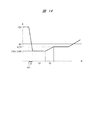
自動車に搭載されたバッテリーのバッテリー電圧は、常に変動する。例えば、エンジンを起動(ON)するために、セルモーターを起動させると、セルモーターを流れる電流が大きくなり、セルモーターとバッテリーとを接続するハーネスにおける電圧降下が大きくなるため、スイッチング電源に給電されているバッテリー電圧が急激に変化する。また、起動後、セルモーターを流れる電流は徐々に減るため、スイッチング電源に給電されているバッテリー電圧も徐々に変化する。従って、バッテリー電圧は、時間に伴って変動することになる。このようなバッテリー電圧の変動は大きく、世界標準規格(ISO)においても、電圧降下の規格化が行われている。 The battery voltage of a battery mounted on a car constantly fluctuates. For example, when the cell motor is started to turn on the engine (ON), the current flowing through the cell motor is increased, and the voltage drop in the harness connecting the cell motor and the battery is increased. Battery voltage changes rapidly. In addition, since the current flowing through the cell motor gradually decreases after startup, the battery voltage supplied to the switching power supply also gradually changes. Thus, the battery voltage will fluctuate with time. Such fluctuations in battery voltage are large, and standardization of voltage drop is also performed in the global standard (ISO).
図14は、ISOの規格で提示されている電圧降下によるバッテリー電圧の変化を示す特性図である。同図において、横軸は時間を示し、縦軸はバッテリー電圧を示している。ここでは、バッテリー電圧は12(V)である。時刻tonにおいて、エンジンをONした場合、期間t1において、バッテリー電圧は12(V)から急激に低下し、3.6(v)または2.6(V)に到達し、その後、時間の経過(t2、t3)とともに、バッテリー電圧は次第に上昇する。 FIG. 14 is a characteristic diagram showing a change in battery voltage due to the voltage drop presented in the ISO standard. In the figure, the horizontal axis indicates time, and the vertical axis indicates battery voltage. Here, the battery voltage is 12 (V). When the engine is turned on at time ton, the battery voltage rapidly decreases from 12 (V) to 3.6 (v) or 2.6 (V) in period t1, and thereafter, the passage of time (time The battery voltage gradually rises with t2 and t3).
車載のスイッチング電源は、このような変動するバッテリー電圧から安定した出力電圧を形成することになる。 On-board switching power supplies will form a stable output voltage from such fluctuating battery voltages.
特許文献1に記載されているスイッチング電源を例にして、スイッチング電源の構成を説明すると次の通りである。ここでは、特許文献1の図2を参照にして説明する。以下の説明において、()内の符号は、特許文献1の図2で用いられている符号に対応している。なお、特許文献1では、スイッチング電源をDC−DCコンバータと称しているが、ここではスイッチング電源として説明する。
The configuration of the switching power supply will be described as follows, taking the switching power supply described in
スイッチング電源は、誤差アンプ(17)、スロープ補償回路(13)、PWMコンパレータ(21)、RSラッチ(22)、出力パワーMOS(24、25)および出力パワーMOS駆動ドライバ(23)等を備えている。誤差アンプ(17)は、出力電圧(VOUT)に基づいた電圧と出力電圧用DAC(12)の出力を比較し、出力パワーMOS(24、25)を制御する電圧帰還部を構成している。また、PWMコンパレータ(21)は、誤差アンプ(17)の出力とスロープ補償回路(13)の出力との差分とコイル電流情報(またはスイッチ電流情報)とを比較し、出力パワーMOS(24、25)を制御する電流帰還部を構成している。すなわち、スイッチング電源は、電圧帰還部と電流帰還部とを含むPWM帰還制御部によって構成されている。 The switching power supply includes an error amplifier (17), a slope compensation circuit (13), a PWM comparator (21), an RS latch (22), an output power MOS (24, 25), an output power MOS drive driver (23), etc. There is. The error amplifier (17) compares the voltage based on the output voltage (VOUT) with the output of the output voltage DAC (12) to configure a voltage feedback unit that controls the output power MOS (24, 25). The PWM comparator (21) compares the difference between the output of the error amplifier (17) and the output of the slope compensation circuit (13) with the coil current information (or switch current information), and outputs an output power MOS (24, 25). ) Constitutes a current feedback unit for controlling the That is, the switching power supply is constituted by a PWM feedback control unit including a voltage feedback unit and a current feedback unit.
スイッチング電源の出力電圧を安定にするためには、このPWM帰還制御部の特性が重要となる。具体的に述べると、PWM帰還制御部のゲインと位相が、発振を起こさないように設定することが重要である。すなわち、ゲインを持つ周波数領域において、位相のずれ(フェーズマージン)が、発振条件である180(deg)に対して余裕を持つように設定することが重要である。 The characteristics of the PWM feedback control unit are important to stabilize the output voltage of the switching power supply. Specifically, it is important to set the gain and phase of the PWM feedback control unit not to cause oscillation. That is, it is important to set the phase shift (phase margin) to have a margin for 180 (deg) which is the oscillation condition in the frequency domain having a gain.
特許文献1の場合には、位相補償抵抗(18)と位相補償コンデンサ(19)が、PWM帰還制御部の位相ずれを補償する位相補償回路として設けられている。このようなスイッチング電源を車載する場合、スイッチング電源の出力電圧を安定化するために、PWM帰還制御部のPWM帰還特性が安定化するように、位相補償抵抗(18)と位相補償コンデンサ(19)の値を設定することになる。
In the case of
上記したように、車載のバッテリー電圧は変動する。図14では、12(V)から3.6(V)まで変動する例を示したが、実使用では、バッテリー電圧は、例えば40(V)から3.2(V)まで変動する。また、ECU内の電子装置の動作に伴って、スイッチング電源から電子装置へ供給する出力電流(負荷電流)も変化する。バッテリー電圧の変動または/および負荷電流の変化により、出力パワーMOS(24、25)または/および出力パワーMOS駆動ドライバ(23)の特性も変化することになる。出力パワーMOSまたは/および出力パワーMOS駆動ドライバの特性が変化することにより、PWM帰還制御部のPWM帰還特性も変化することになるため、PWM帰還制御部のフェーズマージンも変化することになる。 As described above, the on-board battery voltage fluctuates. Although FIG. 14 shows an example of variation from 12 (V) to 3.6 (V), in actual use, the battery voltage varies, for example, from 40 (V) to 3.2 (V). Further, in accordance with the operation of the electronic device in the ECU, the output current (load current) supplied from the switching power supply to the electronic device also changes. Due to the fluctuation of the battery voltage or / and the change of the load current, the characteristics of the output power MOS (24, 25) or / and the output power MOS driver (23) also change. By changing the characteristics of the output power MOS and / or the output power MOS driver, the PWM feedback characteristics of the PWM feedback control unit also change, so the phase margin of the PWM feedback control unit also changes.
位相補償抵抗および位相補償コンデンサの値は、所定のバッテリー電圧で所定の負荷電流を前提として、そのときのフェーズマージンが最適となるように設定される。そのため、例えばバッテリー電圧が変動して、最大の電圧値になったとき、あるいは最小の電圧値になったときには、フェーズマージンが最適になっていないことが考えられる。もし、フェーズマージンが良くなければ、例えばバッテリー電圧の変動が、スイッチング電源の出力電圧に現れ、変動を抑制することが難しくなる。この場合、スイッチング電源の出力電圧を電源電圧として動作している電子装置(プロセッサ等)や車載のセンサ等が、所望の動作をせずに、誤動作を起こし、最悪の場合はシステムダウンにも繋がる。 The values of the phase compensation resistor and the phase compensation capacitor are set such that the phase margin at that time is optimal, assuming a predetermined load current at a predetermined battery voltage. Therefore, for example, when the battery voltage fluctuates to reach the maximum voltage value or the minimum voltage value, it is conceivable that the phase margin is not optimum. If the phase margin is not good, for example, a change in battery voltage appears in the output voltage of the switching power supply, making it difficult to suppress the change. In this case, an electronic device (processor or the like) operating with the output voltage of the switching power supply as a power supply voltage or an on-vehicle sensor causes a malfunction without performing a desired operation, leading to a system shutdown in the worst case. .
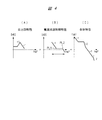
図13は、位相補償抵抗および位相補償コンデンサの値を変更せずに、すなわち、位相補償回路の特性を変更せずに、バッテリー電圧および負荷電流か変化したときのスイッチング電源の特性を示す特性図である。図13(A)は、バッテリー電圧が14(V)で、負荷電流が4(A)の場合を示し、図13(B)は、バッテリー電圧が26(V)に変化し、負荷電流が8(A)に変化した場合を示している。図13(A)および13(B)において、横軸は周波数を示し、左側の縦軸はPWM帰還制御部のゲインを示し、右側の縦軸はPWM帰還制御部の位相を示している。横軸において、例えば1E+2Hzは、10の2乗(Hz)=100(Hz)を示し、1E+3Hzは、10の3乗(Hz)=1000(Hz)を示している。以降、周波数については、同様な表示形式を用いる。 FIG. 13 is a characteristic diagram showing the characteristics of the switching power supply when the battery voltage and the load current are changed without changing the values of the phase compensation resistor and the phase compensation capacitor, that is, without changing the characteristics of the phase compensation circuit. It is. FIG. 13A shows the case where the battery voltage is 14 (V) and the load current is 4 (A), and FIG. 13 (B) shows the case where the battery voltage changes to 26 (V) and the load current is 8 The case where it changed to (A) is shown. 13A and 13B, the horizontal axis indicates frequency, the vertical axis on the left indicates the gain of the PWM feedback control unit, and the vertical axis on the right indicates the phase of the PWM feedback control unit. In the horizontal axis, for example, 1E + 2 Hz indicates 10 2 (Hz) = 100 (Hz), and 1E + 3 Hz indicates 10 3 (Hz) = 1000 (Hz). Hereafter, the same display format is used for the frequency.
図13(A)および13(B)において、実線は、ゲインを示し、破線は位相を示している。図13(A)では、PWM帰還制御部がゲインを持っている期間、すなわち、ゲイン曲線(実線)が、0(dB)を超えている期間(1E+2(Hz)〜約1E+4(Hz))において、位相は発振条件である180(deg)よりも小さい約120(deg)である。これに対して、バッテリー電圧および負荷電流が変化すると、図13(B)に示すように、ゲインを持っている期間(1E+2(Hz)〜約1E+4(Hz))において、最も変化したときの位相は、190(deg)に到達する。この場合、発振条件を超えることになり、PWM期間制御部は発振を起こすことが考えられ、システムダウンに繋がることが考えられる。 In FIGS. 13A and 13B, the solid line indicates the gain, and the broken line indicates the phase. In FIG. 13A, a period in which the PWM feedback control unit has a gain, that is, a period (1E + 2 (Hz) to about 1E + 4 (Hz)) in which the gain curve (solid line) exceeds 0 (dB) The phase is about 120 (deg) which is smaller than 180 (deg) which is the oscillation condition. On the other hand, when the battery voltage and the load current change, as shown in FIG. 13B, the phase when most changed in the period (1E + 2 (Hz) to about 1E + 4 (Hz)) having the gain Reaches 190 (deg). In this case, the oscillation condition is exceeded, and the PWM period control unit is considered to cause oscillation, which may lead to system shutdown.
特許文献1は、バッテリー電圧の変動により生じる課題を認識していない。また、特許文献2は、電流検出回路におけるゲインおよびオフセットの変動を補正することを示しているが、バッテリー電圧の変動により生じる課題を認識していない。
The
その他の課題と新規な特徴は、本明細書の記述および添付図面から明らかになるであろう。 Other problems and novel features will be apparent from the description of the present specification and the accompanying drawings.
一実施の形態に係わる半導体装置を述べると、次のとおりである。 The semiconductor device according to one embodiment is as follows.
すなわち、バッテリー電圧が供給されるスイッチと、スイッチを制御するPWM帰還制御部とを備える電源回路の電源電圧安定化方法は、PWM帰還制御部として、電源回路から出力される電源電圧に基づいて制御を行う電圧帰還制御器と、電源回路から出力される電流に基づいて制御を行う電流帰還制御器とを備え、バッテリー電圧の変動または/および電源回路の負荷条件の変化を検出し、検出結果に従って、PWM帰還制御部の帯域を動的に変更する。 That is, the power supply voltage stabilization method of the power supply circuit including the switch to which the battery voltage is supplied and the PWM feedback control unit controlling the switch is controlled based on the power supply voltage output from the power supply circuit as the PWM feedback control unit. And a current feedback controller that performs control based on the current output from the power supply circuit, and detects a change in battery voltage or / and a change in load condition of the power supply circuit, according to the detection result Dynamically change the bandwidth of the PWM feedback control unit.
PWM帰還制御部の帯域は、PWM帰還制御部のゲインと位相によって表される。ゲインまたは/および位相を動的に変更することにより、バッテリー電圧の変動または/および負荷条件の変化に見合ったPWM帰還特性を提供することが可能となる。 The bandwidth of the PWM feedback control unit is represented by the gain and phase of the PWM feedback control unit. By dynamically changing the gain or / and the phase, it is possible to provide a PWM feedback characteristic commensurate with changes in battery voltage or / and load conditions.
一実施の形態によれば、バッテリー電圧の変動または/および負荷条件が変化しても、電源回路の性能の低下を抑制することが可能な電源電圧安定化方法を提供することができる。 According to one embodiment, it is possible to provide a power supply voltage stabilization method capable of suppressing deterioration in performance of the power supply circuit even if battery voltage fluctuations or / and load conditions change.
以下、本発明の各実施の形態について、図面を参照しつつ説明する。なお、開示はあくまでも一例にすぎず、当業者において、発明の主旨を保っての適宜変更について容易に想到し得るものについては、当然に本発明の範囲に含有されるものである。また、図面は説明をより明確にするため、実際の態様に比べ、各部の幅、厚さ、形状等について模式的に表される場合があるが、あくまで一例であって、本発明の解釈を限定するものではない。 Hereinafter, embodiments of the present invention will be described with reference to the drawings. The disclosure is merely an example, and it is naturally included within the scope of the present invention as to what can be easily conceived of by those skilled in the art as to appropriate changes while maintaining the gist of the invention. In addition, the drawings may be schematically represented as to the width, thickness, shape, etc. of each portion in comparison with the actual embodiment in order to clarify the description, but this is merely an example, and the interpretation of the present invention is not limited. It is not limited.
また、本明細書と各図において、既出の図に関して前述したものと同様の要素には、同一の符号を付して、詳細な説明を適宜省略することがある。 In the specification and the drawings, the same elements as those described above with reference to the drawings already described may be denoted by the same reference numerals, and the detailed description may be appropriately omitted.
以下の説明では、スイッチング電源を、デジタル回路によって構成した場合を例にして説明するが、これに限定されるものではない。すなわち、スイッチング電源を、例えば特許文献1に示されているようなアナログ回路によって構成するようにしてもよい。しかしながら、実現の容易性から、デジタル回路によって構成することが望ましい。また、ここでは、車載のスイッチング電源を例として説明する。
In the following description, the switching power supply is described as an example of a digital circuit, but the present invention is not limited to this. That is, the switching power supply may be configured by an analog circuit as shown, for example, in
(実施の形態1)
<スイッチング電源の構成>
図1は、実施の形態1に係わるスイッチング電源の構成を示すブロック図である。スイッチング電源(電源回路)100は、半導体装置1と、半導体装置1に接続された複数の電子部品を備えている。スイッチング電源100には、バッテリー30が接続され、バッテリー30からバッテリー電圧Vinが給電される。また、スイッチング電源100には、目標設定器40から目標とする電圧値Vrefが供給され、スイッチング電源100は、バッテリー電圧Vinから、目標電圧値Vrefに対応した電圧を形成し、出力電圧(以下、電源電圧とも称する)Voutとして出力する。同図では省略しているが、バッテリー30は、ハーネスによってセルモーター等にも接続され、バッテリー電圧はセルモーター等の電源電圧として給電されている。一方、スイッチング電源100の出力電圧Voutは、ECU内の電子装置およびセンサ等に、それぞれの電源電圧として給電されている。
<Configuration of switching power supply>
FIG. 1 is a block diagram showing the configuration of the switching power supply according to the first embodiment. The switching power supply (power supply circuit) 100 includes a
半導体装置1は、Digitally adjusted Pulse−Width Modulation(以下、パルス幅変調器またはDPWMと称する)4、電流帰還制御器3、電圧帰還制御器2、パラメータ制御器10および加算器9を備えている。特に制限されないが、これらの回路ブロックは、周知の半導体製造技術によって、1つの半導体チップに形成され、半導体装置1となっている。スイッチング電源100を構成するために、半導体装置1の外部には、アナログ/デジタル変換回路(以下、A/D変換回路と称する)5、6および21、加算器22、センサ8、ローパスフィルタ7、抵抗17、18および電圧出力回路50が設けられている。
The
電圧出力回路50は、特に制限されないが、4個のNチャンネル型MOSFET(電界効果型トランジスタ、以下、Nチャンネル型MOSFETは、単にMOSとも称する)11、12、14、15、インバータ回路13、16、インダクタンス20および容量19を備えている。出力用のパワーMOS(以下、出力パワーMOSまたはスイッチと称する)11のソースは、出力パワーMOS12のドレインに接続され、出力パワーMOS11と出力パワーMOS12との間の接続ノードは、分流部23およびインダクタンス20を介して、MOS15のドレインに接続されている。インダクタンス20とMOS15のドレインとの間の接続ノードは、MOS14を介して、接地電圧Vsに接続され、MOS15のソースは平滑用容量19を介して接地電圧Vsに接続されている。MOS15のソースと平滑用容量19との間の接続ノードが、スイッチング電源100の出力ノードとなり、出力ノードから出力電圧Voutが出力される。
The
出力パワーMOS12のソースは、接地電圧Vsに接続され、そのゲートには、インバータ回路13を介してDPWM4の第1出力信号OT1が供給されている。一方、出力パワーMOS11のゲートには、DPWM4の第1出力信号OT1が供給されている。また、MOS15のゲートには、インバータ回路16を介して、DPWM4の第2出力信号OT2が供給され、MOS14のゲートには、DPWM4の第2出力信号OT2が供給されている。
The source of the
DPWM4は、PWM帰還制御により、バッテリー電圧Vinと目標電圧値Vrefとの間の電位差に応じたパルス幅の第1出力信号OT1および第2出力信号OT2を出力する。第1出力信号OT1によって、出力パワーMOS11と12は相補的にオン状態/オフ状態となる、すなわち、出力パワーMOS11(12)がオン状態のとき、出力パワーMOS12(11)はオフ状態となる。同様に、第2出力信号OT2によって、MOS14と15は相補的にオン状態/オフ状態となる。例えば、出力パワーMOS11とMOS14がオン状態となることにより、バッテリー電圧Vinに応じた電流が、分流部23およびインダクタンス20を介して、バッテリー電圧Vinから接地電圧Vsに向かって流れる。この間MOS15はオフ状態となり、平滑用容量19に蓄えた電荷により出力ノードに電圧Voutが出力される。一方、出力パワーMOS12とMOS15がオン状態となると、インダクタンス20および分流部23を介して、接地電圧Vsノードから出力ノードに向かって電流が流れることになる。この間MOS14はオフ状態となり、上記出力ノード電流により平滑用容量19に電荷が充電され、電圧Voutも出力される。DPWM4から出力される第1出力信号OT1と第2出力信号OT2に従って、上記した動作が繰り返され、出力ノードにおける出力電圧Voutは、目標電圧Vrefに対応した電圧値となる。
The
抵抗17、18は、出力ノードと接地電圧Vsとの間で直列的に接続されている。抵抗17、18は、出力電圧Voutを分圧する分圧抵抗として機能する。すなわち、抵抗17と18によって、出力電圧Voutが分圧される。分圧により得られた電圧は、検出電圧として加算器22の負入力に供給されている。この実施の形態においては、抵抗18は、可変抵抗とされている。そのため、抵抗18の抵抗値を変えることにより、加算器22の負入力に供給される検出電圧の値を変更することが可能となっている。
The
加算器22は、目標設定器40から出力されている目標電圧値Vrefと検出電圧とを加算する。検出電圧が、負入力に供給されているため、加算器22は目標電圧値Vrefから、検出電圧を減算するように機能する。この減算により求められた電位差は、A/D変換回路21に供給され、デジタル信号に変換され、半導体装置1内の電圧帰還制御器2に、PWM帰還制御用出力電圧として供給される。電圧帰還制御器2は、供給されたPWM帰還制御用出力電圧に基づいた出力信号を加算器9に供給する。
The
分流部23では、インダクタンス20を流れる負荷電流を分流し、分流により得られた検出電流が、センサ8に供給される。センサ8では、特に制限されないが、検出電流を電圧に変換し、変換により得られた電圧(以下、検出電流電圧または電流検出信号と称する)をローパスフィルタ7へ供給する。ローパスフィルタ7を介した検出電流電圧は、A/D変換回路6によって、デジタル信号に変換され、加算器9の負入力に供給される。
In the
加算器9において、電圧帰還制御器2から出力されている出力信号から、検出電流電圧に相当するデジタル信号が減算され、電流帰還制御器3に供給される。電流帰還制御器3は、電圧帰還制御器2からの出力信号と検出電流電圧に相当するデジタル信号との差分に基づいた出力信号を形成し、DPWM4へ供給する。
In the
目標電圧値Vrefと出力電圧Voutの電圧値との差が小さくなるように、電圧帰還制御が行われる。この実施の形態においては、電圧帰還制御の経路は、加算器22、A/D変換回路21、電圧帰還制御器2、DPWM4、電圧出力回路50によって構成されている。電圧帰還制御は、分圧により形成された検出電圧と目標電圧Vrefとの差分が減少するように、電圧出力回路50を制御する。
The voltage feedback control is performed such that the difference between the target voltage value Vref and the voltage value of the output voltage Vout is reduced. In this embodiment, the path for voltage feedback control is constituted by the
一方、電流帰還制御は、スイッチング電源から出力される負荷電流を制御することにより、出力電圧Voutが安定するように制御する。この実施の形態においては、電流帰還制御の経路は、加算器9、電流帰還制御器3、DPWM4、出力パワーMOS11,12、センサ8、ローパスフィルタ7およびA/D変換回路6によって構成されている。この場合、電流帰還制御は、分流により求められた検出電流電圧と電圧帰還制御器2からの出力信号との差分が減少するように、電圧出力回路50を制御する。このように、実施の形態に係わるスイッチング電源100におけるPWM帰還制御部は、電圧帰還制御を行う電圧帰還制御部と電流帰還制御を行う電流帰還制御部とを備えている。また、電圧帰還制御部は、電圧帰還制御器2を備え、電流帰還制御部は、電流帰還制御器3を備えている。
On the other hand, the current feedback control controls the output voltage Vout to be stable by controlling the load current output from the switching power supply. In this embodiment, the current feedback control path is constituted by the
この実施の形態においては、電流帰還制御器3は、可変型の電流帰還制御器によって構成されており、パラメータ制御器10から供給されるパラメータの値に従って、特性が設定される。パラメータの値によって、電流帰還制御器の特性を変更することにより、PWM帰還制御部の特性を変更するものである。
In this embodiment, the
この実施の形態に係わるパラメータ制御器10には、予め複数のパラメータが設定されている。パラメータ制御器10は、設定されている複数のパラメータから、そのときのスイッチング電源10の動作状態に応じたパラメータを選択し、選択したパラメータの値を、電流帰還制御器3に設定する。スイッチング電源100の動作状態を検出する情報として、パラメータ制御器10は、バッテリー電圧Vinに係わる情報と負荷電流に係わる情報を用いる。これにより、バッテリー電圧Vinの変動または/および負荷電流(負荷条件)の変化に従って、動的に電流帰還制御器3の特性が変更され、その結果としてPWM帰還制御部の特性も動的に変更される。
In the
具体的に述べると、バッテリー電圧Vinは、A/D変換回路5によって、デジタル信号に変換され、変換によって得られたバッテリー検出信号と、上記した検出電流電圧が、パラメータ制御器10に供給される。ここで、バッテリー検出信号が、バッテリー電圧Vinに係わる情報であり、検出電流電圧が、負荷電流に係わる情報である。パラメータ制御器10は、バッテリー検出信号と検出電流電圧に基づいて、パラメータを選択し、電流帰還制御器3に設定する。パラメータ制御器10は、電流帰還制御器3に設定されているパラメータを、新たなパラメータに設定するため、パラメータ制御器10は、電流帰還制御器3のパラメータを動的に書き換えていると見なすこともできる。ここでは、バッテリー電圧Vinの変動および負荷電流の変化を検出する検出信号として、バッテリー検出信号および検出電流電圧を例にして説明するが、これに限定されるものではない。なお、この実施例においては、検出電流電圧は、電流帰還制御とパラメータ変更の両方において兼用されていることになる。
Specifically, the battery voltage Vin is converted into a digital signal by the A /
電流帰還制御器3のパラメータを書き換えることにより、電流帰還制御器3が出力する出力信号が変化し、DPWM4が出力する第1出力信号OT1および第2出力信号OT2が変化する。これにより、PWM帰還制御部の特性である帯域が、そのときのスイッチング電源100の動作状態に対して最適となるように変更される。帯域は、PWM帰還制御部のゲインと位相によって定められるため、より具体的には、電流帰還制御器3のパラメータを書き換えることにより、PWM帰還制御部のゲインと位相が、最適な値に変更されることになる。
By rewriting the parameters of the
次に、電流帰還制御器3およびパラメータ制御器10の具体的な一例を説明する。先ず、電流帰還制御器3の構成を説明する。以降の説明では、1個のパラメータが、2個の電流制御パラメータ、すなわち電流制御パラメータ1および電流制御パラメータ2によって構成されている場合を説明する。
Next, a specific example of the
<電流帰還制御器の構成>
図2は、実施の形態1に係わる電流帰還制御器の構成を示すブロック図である。同図において、3−1、3−2は乗算器を示し、3−3、3−4は加算器を示し、3−5は遅延回路(Z−1)を示している。なお、信号線に付された斜線は、信号が複数であることを示している。
<Configuration of current feedback controller>
FIG. 2 is a block diagram showing the configuration of the current feedback controller according to the first embodiment. In the figure, 3-1 and 3-2 indicate multipliers, 3-3 and 3-4 indicate adders, and 3-5 indicate a delay circuit (Z- 1 ). The oblique lines attached to the signal lines indicate that there are a plurality of signals.
加算器9から出力された信号は、2つに分岐し、一方の信号は、乗算器3−1に供給される。他方の信号は、乗算器3−2に供給される。乗算器3−1は、電流制御パラメータ1と供給されている信号との間で乗算を実行し、乗算結果を加算器3−4に供給する。乗算器3−2は、電流制御パラメータ2と供給されている信号との間で乗算を実行し、乗算結果を加算器3−3に供給する。加算器3−3の出力は、加算器3−4に供給されるとともに、遅延回路3−5に供給される。遅延回路3−5によって遅延された信号は、加算器3−3に供給される。これにより、加算器3−3では、1サイクル遅延した信号との加算が行われる。加算器3−4では、乗算器3−1からの信号と加算器3−3からの信号とを加算し、加算の結果を、電流帰還制御器3の出力信号として、DPWM4へ出力する。
The signal output from the
この実施の形態に係わる電流帰還制御器3においては、電流制御パラメータ1によって、主にゲインが調整され、電流制御パラメータ1および2によって主に位相が調整される。
In the
<パラメータ制御器>
パラメータ制御器10には、予め複数のパラメータが設定されている。より具体的に述べると、パラメータ制御器10は、複数のパラメータが設定されたテーブルを備えている。図3は、実施の形態1に係わるパラメータ制御器が備えるテーブルを示す図である。テーブルの項目としては、パラメータNo.、バッテリー電圧Vin(V)、出力電流(A)、電流制御パラメータ1および電流制御パラメータ2がある。ここで、出力電流(A)は、スイッチング電源100から出力される電流を示し、負荷電流に相当する。
<Parameter controller>
The
テーブルにおいては、バッテリー電圧ごとに、出力電流、電流制御パラメータ1および電流制御パラメータ2が設定されている。すなわち、バッテリー電圧ごとに、出力電流が分類され、出力電流ごとに、電流制御パラメータ1および電流制御パラメータ2が設定されている。例えば、バッテリー電圧Vinが、14(V)未満の場合を例にして説明すると、出力電流が2(A)〜3(A)未満と、1(A)〜2(A)未満と、0(A)〜1(A)未満に分類されている。この分類において、出力電流が2(A)〜3(A)未満の場合には、電流制御パラメータ1は、“0101”で、電流制御パラメータ2は、“01010”であり、出力電流が1(A)〜2(A)未満の場合には、電流制御パラメータ1は、“0110”で、電流制御パラメータ2は、“01100”である。また、出力電流が0(A)〜1(A)未満の場合には、電流制御パラメータ1は、“0111”で、電流制御パラメータ2は、“01110”である。
In the table, an output current, a
以下、同様にして、各バッテリー電圧Vinごと(14(V)〜26(V)未満、26(V)〜40(V)未満)で、出力電流の範囲によって分類され、それぞれに電流制御パラメータ1および2が設定されている。
Similarly, each battery voltage Vin (14 (V) to less than 26 (V), less than 26 (V) to less than 40 (V)) is classified according to the range of output current, and each
また、バッテリー電圧Vinが、例えば40(V)以上では、スイッチング電源100の規格を外れることになる。規格を外れたバッテリー電圧の場合を考慮して、テーブルには、規格外の場合のバッテリー電圧、負荷電流および対応する電流制御パラメータ1および2が設定されている。
In addition, when the battery voltage Vin is, for example, 40 (V) or more, the standard of the switching
電流制御パラメータ1および2は、そのときのバッテリー電圧および出力電流で、PWM帰還制御部が最適な帯域となるような値を予め求め、図2に示したテーブルに格納しておく。
The
<パラメータの書き換え>
パラメータ制御器10は、A/D変換回路5から供給されるバッテリー検出信号と、A/D変換回路6から供給される検出電流電圧に基づいて、図3に示したテーブルを検索し、パラメータNo.を選択する。パラメータ制御器10は、選択したパラメータNo.における電流制御パラメータ1および2が、図2に示した乗算器3−1および3−2に供給されるように、パラメータの書き換えを実行する。
<Rewriting parameters>
The
例えば、パラメータNo.#2の電流制御パラメータ1“0110”および2“01100”が、電流帰還制御器3に設定されている状況で、出力電流が2(A)〜3(A)の間に変化した場合、パラメータ制御器10は、この変化を検出電流電圧によって把握し、変化した出力電流に対応するパラメータNo.#1を選択し、電流制御パラメータ1を“0101”に変更し、電流制御パラメータ2を“01010”に変更する。これにより、電流帰還制御器3の電流制御パラメータ1および2が、選択されたパラメータNo.の電流制御パラメータに書き換えられる。パラメータNo.#1の電流制御パラメータ1および2へ書き換える例を示したが、他のパラメータNo.の場合も同様である。
For example, parameter No. When the output current changes between 2 (A) and 3 (A) in a situation where the
また、バッテリー検出信号によって、バッテリー電圧Vinの変動を検出した場合も、同様、変動したバッテリー電圧Vinに対応するパラメータNo.を、テーブルから検索し、選択したパラメータNo.の電流制御パラメータ1および2で、電流帰還制御器3のパラメータを書き換える。
Also, when a change in the battery voltage Vin is detected by the battery detection signal, the parameter No. 1 corresponding to the changed battery voltage Vin is similarly obtained. Is searched from the table, and the selected parameter No. The parameters of the
バッテリー電圧Vinが、大きく変動した場合には、パラメータ制御器10は、エラーが発生したとして、パラメータNo.#0を選択して、スイッチング電源100の動作を停止させるようにしてもよい。例えば、バッテリー検出信号によって表されるバッテリー電圧Vinが、テーブルにおいて異なる電圧範囲の値に変化した場合、パラメータ制御器10は、バッテリー電圧Vinが大きく変動したとして、パラメータNo.#0を選択する。一例を述べると、バッテリー電圧Vinが、14(V)未満から、異なる電圧範囲である14(V)以上に変動したことを検出した場合、パラメータ制御器10は、パラメータNo.#0を選択する。パラメータNo.#0が選択されることにより、電流帰還制御器3を停止させる電流制御パラメータ1および2が電流帰還制御器3に供給され、電流帰還制御器3の電流制御パラメータが、(停止)の電流制御パラメータ1および2に書き換えられる。これにより、電流帰還制御器3は停止し、その結果としてスイッチング電源100が停止する。
If the battery voltage Vin greatly fluctuates, the
同様に、バッテリー検出信号が40(V)以上のような電圧を示した場合または/および検出電流電圧が、3(A)以上のような電流を示した場合、パラメータ制御器10は、電流制御パラメータ1および2の値として、(停止)を示す“0000”および“00000”を書き込み、スイッチング電源100の動作を停止させる。
Similarly, when the battery detection signal indicates a voltage such as 40 (V) or more or / and the detection current voltage indicates a current such as 3 (A) or more, the
図4は、実施の形態1に係わるPWM帰還制御部のゲイン−周波数特性を説明するための特性図である。同図において、横軸は周波数を示し、縦軸はゲインを示している。図4(A)は、オープンループ状態の電圧帰還制御器2のゲイン−周波数特性を示し、図4(B)は、オープンループ状態の電流帰還制御器3のゲイン−周波数特性を示している。図4(A)に示したオープンループ状態の電圧帰還制御器2のゲイン特性と図4(B)に示したオープンループ状態の電流帰還制御器3のゲイン特性とを掛け合わせることで、オープンループ状態のPWM帰還制御部のゲイン特性が得られる。図4(C)は、このオープンループ状態のPWM帰還制御部のゲイン−周波数特性を示している。
FIG. 4 is a characteristic diagram for explaining gain-frequency characteristics of the PWM feedback control unit according to the first embodiment. In the figure, the horizontal axis indicates the frequency, and the vertical axis indicates the gain. FIG. 4A shows the gain-frequency characteristic of the
電流パラメータ1および2を変更することにより、図4(B)に示す特性の変化点である極PL1、PL2が、周波数方向(横軸方向)で移動する。これにより、PWM帰還制御部のゲイン−周波数特性も、周波数に沿って移動することになり、全体として最適な特性にすることが可能である。
By changing
図5は、実施の形態1に係わるスイッチング電源の特性を説明するための特性図である。図5において、横軸は周波数を示し、左側の縦軸はゲインを示し、右側の縦軸は位相を示している。図13と同様に、図5においても、実線はゲインの変化を示し、破線は位相の変化を示している。 FIG. 5 is a characteristic diagram for explaining the characteristics of the switching power supply according to the first embodiment. In FIG. 5, the horizontal axis indicates frequency, the left vertical axis indicates gain, and the right vertical axis indicates phase. Similarly to FIG. 13, in FIG. 5 also, the solid line indicates a change in gain, and the broken line indicates a change in phase.
図5(A)は、図13(B)と同じ特性を示している。すなわち、図5(A)は、図13(B)で説明したように、バッテリー電圧が14(V)でスイッチング電源100の出力電流が4(A)の状態から、バッテリー電圧が26(V)で出力電流が8(A)の状態に変わったときのゲイン特性と位相特性を示している。図13(B)で説明したように、ゲインが0(dB)を超えている周波数期間において、位相は190(deg)程度となるときが存在するため、発振状態となることが危惧される。
FIG. 5 (A) shows the same characteristics as FIG. 13 (B). That is, as described with reference to FIG. 13B, FIG. 5A shows a state where the battery voltage is 14V and the output current of the switching
これに対して、実施の形態に係わるスイッチング電源100では、バッテリー電圧Vinおよび出力電流が変化すると、これに合わせて、電流制御パラメータ1および2が変更され、電流帰還制御器3のパタメータが書き換えられる。これにより、図4(B)に示した極PL1、PL2が移動し、スイッチング電源100におけるPWM帰還制御部のゲイン特性および位相特性が変化する。これにより、図5(B)に示すように、ゲインが0(dB)よりも下がる周波数が、1E+4(Hz)よりも若干高くなり、ゲインが0(dB)を超えているときの最大位相は、破線で示すように、ほぼ150(deg)である。この場合、発振条件に達していないため、スイッチング電源100が発振することを防ぐことが可能となるとともに、スイッチング電源の性能の向上を図ることが可能である。
On the other hand, in the switching
すなわち、バッテリー電圧Vinの変動または/および出力電流の変化により偏差する位相を、最適な位相に近づけるようにリカバリすることが可能となる。例えば、スイッチング電源100の出力電流は、スイッチング電源100の負荷条件が変わることにより、変化する。この実施の形態によれば、出力電流が変化しても、動的に電流制御パラメータ1および2が書き換えられ、PWM帰還制御部の位相を最適な値に近づけることが可能である。そのため、位相の偏差によって生じるスイッチング電源100の出力電圧の変動の収束に掛かる時間を短くすることが可能となり、スイッチング電源100の性能の向上を図ることが可能である。
That is, it is possible to recover the phase deviated due to the fluctuation of the battery voltage Vin or / and the change of the output current so as to approach the optimum phase. For example, the output current of the switching
また、この実施の形態においては、電流帰還制御器3および電圧帰還制御器2がデジタル回路によって構成されている。これらの制御器を、一般的なアナログ回路で構成することも可能であるが、回路規模等を考慮すると、実現するのは困難であり、デジタル回路によって構成することが望ましい。
Further, in this embodiment, the
(実施の形態2)
図6は、実施の形態2に係わるスイッチング電源の構成を示すブロック図である。図6は、図1に類似しているので、相異点を主に説明する。
Second Embodiment
FIG. 6 is a block diagram showing the configuration of the switching power supply according to the second embodiment. Since FIG. 6 is similar to FIG. 1, the differences will be mainly described.
図1に示したスイッチング電源においては、パラメータ制御器10が、バッテリー電圧Vinおよび出力電流から一意的に、パラメータを選択し、電流帰還制御器3のパラメータを書き換えるようにしていた。これに対して、この実施の形態に係わるスイッチング電源100においては、パラメータ制御器10でモニターする信号が追加される。すなわち、スイッチング電源100の出力電圧Voutにおけるリップルレベルに基づいた信号が、パラメータ制御器10に供給される。これにより、パラメータ制御器10は、バッテリー電圧Vin、出力電流およびリップルレベルに従って、パラメータを選択し、電流帰還制御器3のパラメータを書き換えることになる。
In the switching power supply shown in FIG. 1, the
また、この実施の形態においては、パラメータ制御器10は、リップルレベルが、所定のパラメータ設定限界を超えているか否かを検出し、超えている場合には、スイッチング電源100を停止する。このとき、半導体装置1は、スイッチング電源100の状態を、その外部に通知する。
Further, in this embodiment, the
図6に示した半導体装置1では、A/D変換回路21の出力信号(PWM帰還制御用出力電圧)が、出力電圧Voutにおけるリップルレベルをモニターする信号として、パラメータ制御器10に供給されている点が、図1の半導体装置1と相違する。また、図6の半導体装置1には、インタフェース回路24が追加されている点も、図1の半導体装置1との相異点である。
In the
A/D変換回路21は、出力電圧Voutの分圧電圧と目標電圧Vrefとの差分に従ったデジタル信号を出力する。そのため、出力電圧Voutにリップルが重畳すると、A/D変換回路21の出力信号は、重畳したリップルレベルに従って変化することになる。
The A /
パラメータ制御器10は、A/D変換回路21の出力信号によって示されるリップルレベルに従って、パラメータを選択し、選択したパラメータで電流帰還制御器3のパラメータを書き換える。このパラメータの選択により、パラメータ1によって、電流帰還制御の
主にゲインが調整され、パラメータ1および2によって主に位相の調整が可能であり、
スイッチング電源として適切な特性が実現できる。
このとき、パラメータ制御器10が選択するパラメータの対象は、図3に示したパラメータを細分したパラメータである。
The
Appropriate characteristics can be realized as a switching power supply.
At this time, the target of the parameter selected by the
パラメータ制御器10が、リップルレベルに従って選択する細分パラメータを、次に説明する。ここでは、図3に示したパラメータNo.#1を例にして説明する。パラメータNo.#1の電流制御パラメータ1および2のそれぞれを、同じ間隔で、19個(+9〜0〜−9)に細分する。細分により得られた19個の細分パラメータにおいて、中心の値の細分パラメータの細分パラメータNo.を##0とし、値の増加する方向で、細分パラメータNo.を、##+1〜##+9とし、値の減少する方向で、細分パラメータNo.を、##−1〜##−9とする。
The subdivision parameters that the
パラメータ制御器10には、リップルレベルに対して、所定の第1しきい値と、当該第1しきい値よりも小さい所定の第2しきい値が設定される。パラメータ制御器10によって、電流帰還制御器3に、パラメータNo.#1のパラメータを書き込む場合を例にして説明する。初期では、パラメータ制御器10は、細分パラメータNo.##0の電流制御パラメータ1および2を、電流帰還制御器3に書き込む。これにより、初期では、PWM帰還制御部の特性は、パラメータNo.#1の中心の値に従って設定されることになる。
A predetermined first threshold and a predetermined second threshold smaller than the first threshold are set in the
パラメータ制御器10は、A/D変換回路21の出力信号によって表されるリップルレベルと設定された第1しきい値とを比較し、第1しきい値を超えていた場合、パラメータ制御器10は、細分パラメータNo.を+1し、+1した細分パラメータを選択して、電流帰還制御器3に書き込む。すなわち、パラメータ制御器10は、細分パラメータNo.##+1を選択し、細分パラメータNo.##+1の電流制御パラメータ1および2を、電流帰還制御器3に書き込む。これにより、電流帰還制御器3およびPWM帰還制御部の特性は、リップルレベルに応じて変更される。
The
リップルレベルが小さくなり、パラメータ制御器10が、第2しきい値よりも低下したと判定した場合、パラメータ制御器10は、細分パラメータNo.を−1し、−1した細分パラメータを選択して、電流帰還制御器3に書き込む。すなわち、パラメータ制御器10は、細分パラメータNo.##0を選択し、細分パラメータNo.##0の電流制御パラメータ1および2を、電流帰還制御器3に書き込む。これにより、PWM帰還制御部の特性は、パラメータNo.#1の中心の値に従って設定されることになる。これにより、電流帰還制御器3およびPWM帰還制御部の特性は、初期の値に戻る。すなわち、リップルレベルの検出に基づいて、電流制御パラメータ1および2は、自動的に変更される。
If the ripple level becomes smaller and the
リップルレベルが+方向に大きくなるのに従って、パラメータ制御器10は、細分パラメータ##+9に向かって、細分パラメータを選択し、電流帰還制御器3に書き込む。これに対して、リップルレベルが−方向に大きくなるのに従って、パラメータ制御器10は、細分パラメータ##−9に向かって、細分パラメータを選択し、電流帰還制御器3に書き込む。
As the ripple level increases in the + direction, the
リップルレベルが、+方向または−方向に変化し、パラメータ制御器10が、細分パラメータNo.##+9または##−9を超えるような細分パラメータを選択するようになった場合、パラメータ制御器10は、パラメータ設定限界を超えたと判断し、パラメータNo.#0を選択する。パラメータNo.#0を選択し、パラメータNO.#0の電流制御パラメータ1および2を電流帰還制御器3に書き込むことにより、電流帰還制御器3およびPWM帰還制御部は動作を停止し、スイッチング電源100は、動作を停止する。このとき、パラメータ制御器10は、このときの状態、例えばパラメータNo.#0を選択した旨あるいはリップルレベルがパラメータ設定限界を超えた旨を、インタフェース回路24を介して、半導体装置1の外部に通知する。半導体装置1の外部へ通知することにより、このスイッチング電源100を用いるシステムに対して、フェイルセーフを掛けることが可能となる。
The ripple level changes in the + direction or the-direction, and the
パラメータNo.#1を例にして説明したが、他のパラメータNo.#2〜#9も同様である。 Parameter No. Although described using # 1 as an example, other parameter nos. The same applies to # 2 to # 9.
この実施の形態では、19個の細分パラメータを例にして説明したが、この数に限定されるものではない。パラメータ設定限界も、細分パラメータNo.##−9または##+9に限定されるものではない。なお、細分パラメータにおける電流制御パラメータ1および2は、例えば、図3に示した電流制御パラメータ1および2に対して、19個の状態を表すことが可能なビット数のビットを追加し、追加したビットも電流制御パラメータ1および2として、電流帰還制御器3に書き込むようにすればよい。
In this embodiment, nineteen subdivision parameters are described as an example, but the number is not limited to this number. Also for the parameter setting limit, subdivision parameter numbers It is not limited to ##-9 or ## + 9. Note that, for the
この実施の形態においては、上記したように第2しきい値が第1しきい値よりも小さくなっている。そのため、リップルレベルの変化に対して、より初期の状態に戻り易くなっている。これは、初期の状態がより安定であるためである。勿論、上記した第1しきい値と第2しきい値は同じであっても、あるいは第2しきい値が第1しきい値よりも大きくてもよい。 In this embodiment, as described above, the second threshold is smaller than the first threshold. Therefore, it is easy to return to the initial state with respect to the change of the ripple level. This is because the initial state is more stable. Of course, the first threshold and the second threshold described above may be the same, or the second threshold may be larger than the first threshold.
この実施の形態においては、スイッチング電源100の出力電圧Voutにおけるリップルレベルもモニターして、PWM帰還制御部の特性が動的に変更される。そのため、スイッチング電源100から出力される出力電流の変化以外の負荷側の変化に対しても、スイッチング電源100は、安定した出力電圧Voutを供給することが可能となる。また、負荷側の変化が大きく、パラメータ設定限界を超えた場合には、システムに対して、フェイルセーフを掛けることが可能であり、安全性の向上を図ることが可能である。
In this embodiment, the ripple level at the output voltage Vout of the switching
(実施の形態3)
実施の形態1および2では、PWM帰還制御部の結果をパラメータ制御器10に供給することにより、電流帰還制御器3のパラメータを書き換える処理に、PWM帰還制御部の結果をフィードバックしていた。フィードバックに応答して、パラメータの書き換えを行うため、結果が反映するまでに遅延が生じ、スイッチング電源100に不安定性が生じることが考えられる。スイッチング電源100が不安定になり、出力電圧Voutが不安定になると、スイッチング電源100の出力電圧Voutで動作しているプロセッサの動作が不安定になったり、スイッチング電源100の出力電圧Voutで動作しているセンサの出力が不正確になることが危惧される。
Third Embodiment
In the first and second embodiments, the result of the PWM feedback control unit is fed back to the
この実施の形態においては、プロセッサが、イベントに対して、次に実行する処理において必要となる電流に見合った電流制御パラメータの設定を実行する。これにより、フィードバック処理ではなく、フィードフォワード処理で、電流帰還制御器3のパラメータを書き換えることが可能となり、スイッチング電源が不安定になるのを低減することが可能となる。次に、図を用いて、この実施の形態に係わるシステムを説明する。
In this embodiment, the processor executes, for the event, setting of current control parameters corresponding to the current required in the process to be performed next. As a result, parameters of the
図7は、実施の形態3に係わる電源システムの構成を示すブロック図である。同図には、スイッチング電源100と、スイッチング電源100からの出力電圧Voutを電源電圧として動作するプロセッサ60およびセンサ70などの周辺デバイスとを備えた電源システム200が示されている。プロセッサ60は、例えばECUに設けられ、センサ70は、例えば自動車に搭載されている。センサ70とプロセッサ60との間では、信号の送受信が行われる。例えば、プロセッサ60は、センサ70に対して車両の情報の取得を指示する信号を送信し、センサ70によって取得された車両の情報が、信号としてプロセッサ60に供給される。プロセッサ60は受信した車両の情報を処理する。
FIG. 7 is a block diagram showing the configuration of the power supply system according to the third embodiment. The figure shows a
スイッチング電源100の構成は、図1に示したスイッチング電源の構成と類似しているので、相異点を主に説明する。相異点は、半導体装置1にインタフェース回路24が追加され、パラメータ制御器10が変更され、パラメータ制御器10Aとなっていることである。
The configuration of the switching
パラメータ制御器10Aは、実施の形態1で説明したパラメータ制御器10と同様に、A/D変換回路5からのバッテリー検出信号とA/D変換回路6からの検出電流電圧に基づいて、パラメータNo.を選択し、選択したパラメータNo.の電流制御パラメータ1および2で、電流帰還制御器3のパラメータを書き換える機能を備えている。さらに、パラメータ制御器10Aには、インタフェース回路24を介してプロセッサ60から電源パラメータ設定指示を受信し、受信した電源パラメータ設定指示に従って、パラメータNo.を選択し、選択したパラメータNo.の電流制御パラメータで、電流帰還制御器3のパラメータを書き換える機能が追加されている。すなわち、パラメータ制御器10Aでは、電源パラメータ設定指示によって、例えば上記した図3に示したパラメータNo.#1〜#9のいずれかが指示される(例えば、#1が指示される)。パラメータ制御器10Aは、指示されたパラメータNo.#1の電流制御パラメータ1および2を、電流帰還制御器3に書き込む。
The
また、パラメータ制御器10Aは、パラメータNo.#0を選択した場合、スイッチング電源100の動作を停止させるとともに、異常が発生したことを、インタフェース回路24を介して、プロセッサ60に通知する。
Further, the
<プロセッサの動作>
図8は、実施の形態3に係わるプロセッサの動作を説明するためのフローチャート図である。プロセッサ60は、ステップS1でイベント要求を受け付ける。イベントは例えばエンジンスタート、セルモータ等の電源投入がある。次に、受け付けたイベント要求に対する準備を、プロセッサ60は、ステップS2で実行する。
<Processor operation>
FIG. 8 is a flowchart for explaining the operation of the processor according to the third embodiment. The
このステップS2の実行において、プロセッサ60は、動作させるセンサ70等の周辺デバイスおよびプロセッサ60の処理で必要となる消費電力を推定する。推定した消費電力に対応するパラメータNo.を、電源パラメータ設定指示として、プロセッサ60は、ステップS3において、半導体装置1に供給する。半導体装置1では、供給された電源パラメータ設定指示が、インタフェース回路24を介して、パラメータ制御器10Aに供給される。パラメータ制御器10Aは、電源パラメータ設定指示に従って、パラメータNo.を選択し、選択したパラメータNo.の電流制御パラメータ1および2で、電流帰還制御器3のパラメータを書き換える。
In the execution of step S2, the
次に、ステップS4で、プロセッサ60は、ステップS1で受け付けたイベントの処理を開始する。インベントを処理するのに、センサ70等の周辺デバイスを起動することが必要となるため、ステップS5において、プロセッサ60は、周辺デバイスを起動させる。このとき、周辺デバイス等が起動するため、スイッチング電源100の負荷電流が増加することになるが、予め、ステップS3において、電流帰還制御器3のパラメータが、消費電力の増加に合わせて、最適な状態に変更されているため、ステップS5においても、スイッチング電源100は、安定して動作することが可能である。
Next, in step S4, the
その後、ステップS6において、受け付けたイベントを実行する。 Thereafter, in step S6, the accepted event is executed.
実施の形態3においては、予め必要なる負荷電流に対応したパラメータが、予め電流帰還制御器3に書き込まれる。すなわち、フィードフォワード処理により、電流帰還制御器3のパラメータが書き込まれる。そのため、フィードバック処理により、パラメータを書き込む場合に比べて、スイッチング電源100は、更に安定した出力電圧を、電源電圧として電源システム200内のプロセッサ60および周辺デバイスへ給電することが可能であり、システムとしての性能の向上を図ることが可能である。例えばS1がエンジンスタートのイベント要求では、図14に示すように、予めバッテリー電圧が低下するのをプロセッサ60やパラメータ制御器10Aで予測出来るので、エンジン始動時の電源制御の乱れを防止出来る。
In the third embodiment, parameters corresponding to the load current required in advance are written to the
もし想定外の負荷、故障が発生し、パラメータ制御器10Aが、パラメータN0.#0を選択した場合には、インタフェース回路24を介して、エラーがプロセッサ60に通知されるため、プロセッサ60は異常を検知することが可能である。通知された異常に対して、プロセッサ60は、実行中のイベントの中断もしくは電源システム200の停止等を早期に対応することが可能となる。車載システムは、安全性が要求されるため、早期に対応が可能な電源システム200は、車載システムとして特に有効である。
If an unexpected load or failure occurs, the
(実施の形態4)
実施の形態1〜3では、電流帰還制御器3のパラメータを書き換える例を示したが、実施の形態4では、電流帰還制御器3と電圧帰還制御器2の双方のパラメータが書き換えられる。
In the first to third embodiments, the parameters of the
図9は、実施の形態4に係わるスイッチング電源の構成を示すブロック図である。図9は、図1と類似しているので、相異点を主に説明する。相異点は、図1に示したパタメータ制御器10が変更され、パラメータ制御器10Bとなっていることと、電圧帰還制御器2が可変型の電圧帰還制御器に変更されていることである。
FIG. 9 is a block diagram showing the configuration of the switching power supply according to the fourth embodiment. Since FIG. 9 is similar to FIG. 1, differences will mainly be described. The difference is that the
この実施の形態に係わる電圧帰還制御器2は、図2で説明した電流帰還制御器3と同様に、2つの電圧制御パラメータによって、そのゲイン−周波数特性が設定される。すなわち、2つの電圧制御パラメータを変更することにより、電圧帰還制御器2のゲイン−周波数特性を動的に変更することができる。
Similar to the
パラメータ制御器10Bは、電流帰還制御器3に対応したテーブルと、電圧帰還制御器2に対応したテーブルとを、別々に備えている。2つのテーブルを区別するために、電流帰還制御器3に対応したテーブルは、以降、電流テーブルと称し、電圧帰還制御器3に対応したテーブルは、以降、電圧テーブルと称する。
The
パラメータ制御器10Bは、A/D変換回路5からのバッテリー検出信号と、A/D変換回路6からの検出電流電圧とに基づいて、電流テーブルおよび電圧テーブルからパラメータを選択し、電流テーブルから選択したパターンNo.の電流制御パターン1および2で、電流帰還制御器3のパターンを書き換える。電流帰還制御器3のパターンの書き換えは、実施の形態1と同じであるため、説明は省略する。
The
図10は、実施の形態4に係わる電圧テーブルを示す図である。電圧テーブルの項目は、図3に示したテーブルと同様に、5つの項目を備えており、項目として、電流制御パラメータ1および2の代わりに、電圧制御パラメータ1および2を備えている。電流制御パラメータ1および2が、電圧制御パラメータ1および2に代わっていることを除いて、電圧テーブルは、電流テーブル(図3のテーブル)と同じであるため、説明は省略する。なお、説明を容易にするために、図10に示した電圧制御パラメータ1および2は、図3に示した電圧制御パラメータ1および2と同じ値となっているが、勿論異なる値であってもよい。
FIG. 10 is a diagram showing a voltage table according to the fourth embodiment. Similar to the table shown in FIG. 3, the items of the voltage table are provided with five items, and the items of
パラメータ制御器10Bは、図10に示した電圧テーブルから選択したパラメータNo.の電圧制御パターン1および2で、電圧帰還制御部2のパラメータを書き換える。これにより、電圧帰還制御器2のゲイン−周波数特性が変更される。
The
この実施の形態によれば、電流帰還制御器3および電圧帰還制御器2の両方の特性が、動的に変更される。そのため、PWM帰還制御部の特性を、動的により細かく変更することが可能である。
According to this embodiment, the characteristics of both
<電流制御パラメータ1および2と電圧制御パラメータ1および2>
ここで、電流制御パラメータ1および2と電圧制御パラメータ1および2について述べておく。
<
Here,
電流帰還制御器3は、出力電流のインダクタンス電流量とターゲット電流量(目標電流量)を比例処理する比例回路と、その差分を積分処理する積分回路によって構成されていると見なすことができる。このように見なした場合、比例回路は、電流制御パラメータ1によって処理ゲインが決定される。また、積分回路は、電流制御パラメータ1および2により位相が決定される。
The
そのため、前記したように、電流制御パラメータ1によって、電流帰還制御部3のゲインが主に調整され、電流制御パラメータ1および2によって、電流帰還制御部3の位相が主に調整される。
Therefore, as described above, the gain of the current
同様に、電圧帰還制御器2も、比例回路と積分回路によって構成されていると見なすことができる。このように見なした場合、比例回路は電圧制御パラメータ1によって処理ゲインが決定され、積分回路は電圧制御パラメータ1および2により位相が決定される。従って、電流制御パラメータ1および2と同様に、電圧制御パラメータ1によって、電圧帰還制御部2のゲインが主に調整され、電圧制御パラメータ1および2によって、電圧帰還制御部2の位相が主に調整される。
Similarly, the
(実施の形態5)
この実施の形態においては、定常状態で、リップルレベルをモニターし、スイッチング電源100の初期バラツキを補正する構成を説明する。初期バラツキを補正することにより、複数のスイッチング電源間で、PWM帰還制御部の特性を均一化することが可能となる。
Fifth Embodiment
In this embodiment, a configuration is described in which the ripple level is monitored in the steady state to correct the initial variation of the switching
図11は、実施の形態5に係わる補正テーブルを示す図である。図11に示した補正テーブルは、図9に示したパラメータ制御器10Bに設けられている。この場合、図3に示した電流テーブルの各パラメータNo.ごとに、図11に示した補正テーブルが設けられている。同様に、図10に示した電圧テーブルの各パラメータNo.ごとに、図11に示した補正テーブルが設けられている。なお、電流テーブルの各パラメータNo.ごとに設けられた補正テーブルにおいては、電圧帰還パラメータ1_Cおよび2_Cは存在しなくてもよい。同様に、電圧テーブルの各パラメータNo.ごとに設けられた補正テーブルにおいては、電流帰還パラメータ1_Cおよび2_Cは存在しなくてもよい。
FIG. 11 shows a correction table according to the fifth embodiment. The correction table shown in FIG. 11 is provided in the
パラメータ制御器10Bは、図3で示した電流テーブルからパラメータNo.を選択して、選択したパラメータNo.の電流制御パラメータ1および2を、電流帰還制御器3に書き込むが、このとき、選択したパラメータNo.に対応する補正テーブルから、電流帰還パラメータ1_Cおよび2_Cを選択し、選択した電流帰還パラメータ1_Cを電流制御パラメータ1とともに、電流帰還制御器3に書き込み、選択した電流帰還パラメータ2_Cを電流制御パラメータ2とともに、電流帰還制御器3に書き込む。この選択した電流帰還パラメータ1_Cは、電流制御パラメータ1の補正パラメータとして機能し、電流帰還パラメータ2_Cは、電流制御パラメータ2の補正パラメータとして機能する。
From the current table shown in FIG. And the selected parameter No.
同様に、パラメータ制御器10Bは、図10で示した電圧テーブルからパラメータNo.を選択して、選択したパラメータNo.の電圧制御パラメータ1および2を、電圧帰還制御器2に書き込むが、このとき、選択したパラメータNo.に対応する補正テーブルから、電圧帰還パラメータ1_Cおよび2_Cを選択し、選択した電圧帰還パラメータ1_Cを電圧制御パラメータ1とともに、電圧帰還制御器2に書き込み、選択した電圧帰還パラメータ2_Cを電圧制御パラメータ2とともに、電圧帰還制御器2に書き込む。この選択した電圧帰還パラメータ1_Cは、電圧制御パラメータ1の補正パラメータとして機能し、電圧帰還パラメータ2_Cは、電圧制御パラメータ2の補正パラメータとして機能する。
Similarly, the
補正テーブルは、補正値ごとに、電流帰還パラメータ1_C、2_Cおよび電圧帰還パラメータ1_Cおよび2_Cが設定される。図11の例では、補正値として、−9%、−6%、−3%、Default、+3%、+6%および+9%が設定され、それぞれの電流帰還パラメータと電圧帰還パラメータが設定されている。補正テーブルからの電流帰還パラメータおよび電圧帰還パラメータの選択は、特に制限されないが、補正値を選択することにより行う。 In the correction table, current feedback parameters 1_C and 2_C and voltage feedback parameters 1_C and 2_C are set for each correction value. In the example of FIG. 11, -9%, -6%, -3%, Default, + 3%, + 6% and + 9% are set as correction values, and respective current feedback parameters and voltage feedback parameters are set. . Selection of the current feedback parameter and the voltage feedback parameter from the correction table is not particularly limited, but is performed by selecting the correction value.
電流テーブルからパラメータNo.を選択したときに、どの補正値を選択するかは、例えば、次に説明するようにリップルレベルをモニターすることにより行う。 Parameter No. from current table. When is selected, which correction value to select is determined, for example, by monitoring the ripple level as described below.
すなわち、所定の条件のときに、スイッチング電源100の出力電圧Voutにおけるリップルレベルが、目標レベル以内に納まるように、補正値を選択する。例えば、電流テーブルのパラメータNo.#1で述べると、パラメータNO.#1の電流制御パラメータ1および2と、補正値がDefaultの電流帰還パラメータ1_Cおよび2_Cを電流帰還制御器3に書き込み、リップルレベルを測定する。測定の結果、リップルレベルが、目標レベル以内に入っていれば、以後は、補正値としてDefaultを選択する。これに対して、測定の結果、リップルレベルが目標レベル以内に入っていない場合には、補正値を変更して、リップルレベルを測定する。以降同様な動作を繰り返して、リップルレベルが目標レベル以内に入る補正値を定める。以降、スイッチング電源100において、パラメータNo.#1が選択されたときには、補正テーブルから、目標レベル以内に入ったときの補正値を選択する。
That is, the correction value is selected such that the ripple level at the output voltage Vout of the switching
電流テーブルのパラメータNo.#2〜#9のそれぞれに対応する補正テーブルおよび電圧テーブルのパラメータNo.#1〜#9のそれぞれに対応する補正テーブルにおいても同様にして、選択する。選択した補正値は、以降、スイッチング電源100において、対応するパラメータNo.が選択されたとき、電流帰還制御器3および電圧帰還制御器2に書き込まれる。
Parameter No. of current table Parameter No. of correction table and voltage table corresponding to each of # 2 to # 9. Similarly, the correction tables corresponding to # 1 to # 9 are selected. Thereafter, in the switching
上記したリップルレベルを用いた補正値の選択は、例えば半導体装置1を生産する段階で実行する。これにより、複数の半導体装置1間でのPWM帰還制御部の特性をトリミングして、バラツキを低減することが可能となる。
The selection of the correction value using the ripple level described above is performed, for example, at the stage of producing the
<変形例>
半導体装置1を生産する段階で、補正値を選択する場合を説明した。半導体装置の特性は、経年変化する。経年変化により、リップルレベルが目標レベル以内から外れたとき、上記した補正値の選択を実施する。
<Modification>
The case of selecting the correction value at the stage of producing the
例えば、セルモーターの起動時(半導体装置1の起動時)のタイミングで、リップルレベルが目標レベル以内に収まるように上記と同様な動作を実行してもよい。
For example, the same operation as described above may be performed so that the ripple level falls within the target level at the time of activation of the cell motor (when the
電流テーブルおよび電圧テーブルにおける各パラメータNo.ごとに、図11に示したテーブルを設ける例を説明したが、これに限定されない。すなわち、各パラメータNo.に対して、補正レジスタを設け、選択した補正値の電流帰還パラメータ1_C、2_Cおよび電圧帰還パラメータ1_C、2_Cを格納するようにしてもよい。この場合には、各パラメータNo.ごとに補正テーブルを設けなくて済むため、半導体装置1の小型化を図ることが可能である。
Parameter No. in current table and voltage table Although the example which provides the table shown in FIG. 11 was demonstrated for every, it is not limited to this. That is, each parameter No. Alternatively, a correction register may be provided to store the current feedback parameters 1_C and 2_C and voltage feedback parameters 1_C and 2_C of the selected correction value. In this case, each parameter No. Since it is not necessary to provide a correction table every time, the
(実施の形態6)
実施の形態1〜5では、パラメータ制御器10(10A、10B)に電流テーブル(電圧テーブル)を設け、これらのテーブルにパラメータを設定する例を説明した。
Sixth Embodiment
In the first to fifth embodiments, the parameter controller 10 (10A, 10B) is provided with the current table (voltage table), and the example in which the parameter is set in these tables has been described.
この実施の形態においては、実施の形態1〜5において、テーブルが、パラメータ制御器10に設けられた複数の内部レジスタによって構成され、プロセッサ60Aが、パラメータを複数の内部レジスタに格納する。
In this embodiment, in the first to fifth embodiments, the table is configured by a plurality of internal registers provided in the
図12は、実施の形態6に係わる電源システムの構成を示す図である。電源システムは、図7に示したように、複数の回路ブロックを備えているが、図12には、説明に必要なパラメータ制御器10Aとプロセッサ60のみが示されている。パラメータ制御器10Aは、電流テーブルを構成する複数の内部レジスタを備えている。図12では、複数の内部レジスタのうち、内部レジスタ10―1および10―2が代表として描かれている。
FIG. 12 is a diagram showing the configuration of a power supply system according to the sixth embodiment. The power supply system is provided with a plurality of circuit blocks as shown in FIG. 7, but only the
プロセッサ10は、電流パラメータ1および2を、インタフェース回路24(図7)を介して、内部レジスタ10―1、10−2に書き込む。パラメータ制御器10Aは、電流帰還制御器3の特性を変更するとき、内部レジスタ10―1、10―2に書き込まれている電流パラメータ1および2を読み出して、電流帰還制御器3に書き込む。なお、プロセッサ60は、スイッチング電源100において、PWM帰還制御部の特性を変更する前に、内部レジスタ10―1、10―2に、電流パラメータを書き込むことになる。
The
ここでは、電流テーブルを例にして説明したが、電圧テーブルおよび補正テーブルも同様である。 Here, although the current table has been described as an example, the same applies to the voltage table and the correction table.
<変形例>
変形例においては、パラメータ制御器10Aが、電気的に書き換え可能な不揮発性メモリ(例えばフラッシュメモリ)を備える。プロセッサ60A等によって、パラメータ制御器10A内の不揮発性メモリに電流パラメータを書き込む。これにより、半導体装置1に電源電圧(例えばバッテリー電圧Vin)が給電されていない状態から、給電された状態に以降したときから、動的にPWM帰還制御部の特性を変更することが可能となる。勿論、この場合、電圧テーブルおよび補正テーブルも同様に、不揮発性メモリによって構成してもよい。
<Modification>
In the modification, the
実施の形態1〜3においては、電流制御パラメータ1および2を例にして説明したが、電流制御パラメータ1および2の代わりに電圧制御パラメータ1および2を用いるようにしてもよい。
In the first to third embodiments, the
本明細書においては、電流帰還制御器3に係わるパラメータを第1パラメータと称し、電圧帰還制御器2に係わるパラメータを第2パラメータと称することがある。例えば、電流制御パラメータ1および2を纏めて、第1パラメータと称し、電圧制御パラメータ1および2を纏めて、第2パラメータと称することがある。
In the present specification, a parameter related to the
以上、本発明者によってなされた発明を実施の形態に基づき具体的に説明したが、本発明は前記実施の形態に限定されるものではなく、その要旨を逸脱しない範囲で種々変更可能であることはいうまでもない。 As mentioned above, although the invention made by the present inventor was concretely explained based on an embodiment, the present invention is not limited to the above-mentioned embodiment, and can be variously changed in the range which does not deviate from the gist. Needless to say.
1 半導体装置
2 電圧帰還制御器
3 電流帰還制御器
4 DPWM
10、10A、10B パラメータ制御器
30 バッテリー
100 スイッチング電源
200 電源システム
Vin バッテリー電圧
Vout 電源電圧
1
10, 10A,
Claims (20)
前記PWM帰還制御部は、前記電源回路から出力される電源電圧に基づいて制御を行う電圧帰還制御器と、前記電源回路から出力される電流に基づいて制御を行う電流帰還制御器とを備え、
前記バッテリー電圧の変動または/および前記電源回路の負荷条件の変化を検出し、
検出の結果に従って、前記PWM帰還制御部の帯域を、動的に変更する、電源電圧安定化方法。 A power supply voltage stabilization method for a power supply circuit, comprising: a switch to which a battery voltage is supplied; and a PWM feedback control unit that controls the switch,
The PWM feedback control unit includes a voltage feedback controller that performs control based on a power supply voltage output from the power supply circuit, and a current feedback controller that performs control based on a current output from the power supply circuit.
Detecting changes in the battery voltage or / and load conditions of the power supply circuit,
A power supply voltage stabilization method, wherein a bandwidth of the PWM feedback control unit is dynamically changed according to a detection result.
前記検出は、前記バッテリー電圧または/および前記電源回路の出力電流に基づいて行う、電源電圧安定化方法。 In the power supply voltage stabilization method according to claim 1,
A power supply voltage stabilization method, wherein the detection is performed based on the battery voltage or / and an output current of the power supply circuit.
前記電流帰還制御器は、第1パラメータに従って特性が変化する可変型の電流帰還制御器であり、前記検出の結果に従って前記第1パラメータが変更される、電源電圧安定化方法。 In the power supply voltage stabilization method according to claim 2,
The power supply voltage stabilization method, wherein the current feedback controller is a variable current feedback controller whose characteristics change according to a first parameter, and the first parameter is changed according to a result of the detection.
前記電源回路は、互いに異なる複数の第1パラメータを予め格納し、前記検出の結果に従って、前記複数の第1パラメータから、前記電流帰還型制御器に供給する第1パラメータを選択する、電源電圧安定化方法。 In the power supply voltage stabilization method according to claim 3,
The power supply circuit stabilizes a plurality of first parameters different from each other in advance, and selects a first parameter to be supplied to the current feedback controller from the plurality of first parameters according to the result of the detection. Method.
前記電圧帰還制御器は、第2パラメータに従って特性が変化する可変型の電圧帰還制御器であり、前記検出の結果に従って前記第2パラメータが変更される、電源電圧安定化方法。 In the power supply voltage stabilization method according to claim 2 or 3,
The voltage feedback controller is a variable voltage feedback controller whose characteristics change according to a second parameter, and the second parameter is changed according to a result of the detection.
前記電源回路は、互いに異なる複数の第2パラメータを予め格納し、前記検出の結果に従って、前記複数の第2パラメータから、前記電圧帰還型制御器に供給する第2パラメータを選択する、電源電圧安定化方法。 In the power supply voltage stabilization method according to claim 4,
The power supply circuit stabilizes a plurality of different second parameters in advance, and selects a second parameter to be supplied to the voltage feedback controller from the plurality of second parameters according to the result of the detection. Method.
前記電源回路から出力される電源電圧のリップルレベルを検出し、前記電流帰還制御器の特性を定める前記第1パラメータまたは/および前記電圧帰還制御部の特性を定める前記第2パラメータを変更する、電源電圧安定化方法。 In the power supply voltage stabilization method according to claim 5,
A power supply that detects a ripple level of a power supply voltage output from the power supply circuit, and changes the first parameter that determines the characteristics of the current feedback controller and / or the second parameter that determines the characteristics of the voltage feedback control unit Voltage stabilization method.
前記電源電圧のリップルレベルの検出の結果に従って、前記第1パラメータまたは/および前記第2パラメータは、自動的に変更される、電源電圧安定化方法。 In the power supply voltage stabilization method according to claim 7,
A power supply voltage stabilization method, wherein the first parameter or / and the second parameter are automatically changed according to a result of detection of a ripple level of the power supply voltage.
前記第1パラメータおよび第2パタメータのそれぞれは、ゲインを定めるパラメータと位相を定めるパラメータを備える、電源電圧安定化方法。 In the power supply voltage stabilization method according to claim 5,
The power supply voltage stabilization method, wherein each of the first parameter and the second parameter comprises a parameter for determining a gain and a parameter for determining a phase.
電圧帰還制御器と、
第1パラメータに従って、その特性が変更される可変型の電流帰還制御器と、
互いに異なる複数の第1パラメータが予め設定されたパラメータ制御器と、
を備え、
前記パルス幅信号によって制御されるスイッチに供給されるバッテリー電圧に基づいたバッテリー検出信号および前記スイッチを介して出力される電流に基づいた電流検出信号に従って、前記パラメータ制御器は、予め設定されている前記複数の第1パラメータから、第1パラメータを選択し、前記電流帰還制御器に設定する、半導体装置。 A pulse width modulator that outputs a pulse width signal according to the difference between the output voltage and the target voltage;
Voltage feedback controller,
A variable current feedback controller whose characteristics are changed according to a first parameter;
A parameter controller in which a plurality of mutually different first parameters are preset;
Equipped with
The parameter controller is preset according to a battery detection signal based on a battery voltage supplied to a switch controlled by the pulse width signal and a current detection signal based on a current output through the switch A semiconductor device which selects a first parameter from the plurality of first parameters and sets the first parameter in the current feedback controller.
前記電圧帰還制御器は、第2パラメータに従って、その特性が変更される可変型の電圧帰還制御器であり、
前記パラメータ制御器は、互いに異なる複数の第2パラメータが予め設定され、前記パラメータ制御器は、予め設定されている前記複数の第2パラメータから、第2パラメータを選択し、前記電圧帰還制御器に設定する、半導体装置。 The semiconductor device according to claim 10,
The voltage feedback controller is a variable voltage feedback controller whose characteristics are changed according to a second parameter,
The parameter controller is preset with a plurality of different second parameters, and the parameter controller selects a second parameter from the plurality of preset second parameters, and the voltage feedback controller selects the second parameter. Semiconductor device to set.
前記電圧帰還制御器には、前記スイッチを介したバッテリー電圧に基づいた前記出力電圧と目標電圧の差分が供給され、
前記電流帰還制御器には、前記電流検出信号と、前記電圧帰還制御器の出力との差分が供給され、
前記パルス幅変調器は、前記電流帰還制御器の出力に従ったパルス幅信号を出力する、半導体装置。 In the semiconductor device according to claim 11,
The voltage feedback controller is supplied with a difference between the output voltage and a target voltage based on a battery voltage via the switch.
The current feedback controller is supplied with the difference between the current detection signal and the output of the voltage feedback controller.
The semiconductor device, wherein the pulse width modulator outputs a pulse width signal according to an output of the current feedback controller.
前記第1パラメータおよび第2パタメータのそれぞれは、ゲインを定めるパラメータと位相を定めるパラメータを備える、半導体装置。 In the semiconductor device according to claim 12,
A semiconductor device, wherein each of the first parameter and the second parameter includes a parameter for determining a gain and a parameter for determining a phase.
前記パラメータ制御器に接続され、半導体装置の外部と前記パラメータ制御器との間で信号のインタフェースを行うインタフェース回路を、さらに備える、半導体装置。 In the semiconductor device according to claim 13,
A semiconductor device, further comprising: an interface circuit connected to the parameter controller to interface a signal between the outside of the semiconductor device and the parameter controller.
前記電流帰還制御器、電圧帰還制御器、前記スイッチおよび前記インタフェース回路は、1つの半導体チップに形成されている、半導体装置。 In the semiconductor device according to claim 14,
The semiconductor device, wherein the current feedback controller, the voltage feedback controller, the switch, and the interface circuit are formed in one semiconductor chip.
前記半導体装置は、
出力電圧と目標電圧との差に従ったパルス幅信号を出力するパルス幅変調器と、
電圧帰還制御器と、
第1パラメータに従って、その特性が変更される可変型の電流帰還制御器と、
前記第1パラメータを前記電流帰還制御器に設定するパラメータ制御器と、
前記パラメータ制御器と前記プロセッサとに接続されるインタフェース回路と、
を備え、
前記パルス幅信号によって制御されるスイッチに供給されるバッテリー電圧に基づいたバッテリー検出信号および前記スイッチを介して出力される電流に基づいた電流検出信号に従って、前記パラメータ制御器は、前記第1パラメータを、前記電流帰還制御器に設定する、電源システム。 What is claimed is: 1. A power supply system comprising a semiconductor device and a processor connected to the semiconductor device, comprising:
The semiconductor device is
A pulse width modulator that outputs a pulse width signal according to the difference between the output voltage and the target voltage;
Voltage feedback controller,
A variable current feedback controller whose characteristics are changed according to a first parameter;
A parameter controller for setting the first parameter to the current feedback controller;
An interface circuit connected to the parameter controller and the processor;
Equipped with
According to a battery detection signal based on a battery voltage supplied to a switch controlled by the pulse width signal and a current detection signal based on a current output through the switch, the parameter controller controls the first parameter , Power supply system to set in the current feedback controller.
前記電圧帰還制御器は、第2パラメータに従って、その特性が変更される可変型の電圧帰還制御器であり、
前記パラメータ制御器は、前記第2パラメータを、前記電圧帰還制御器に設定する、電源システム。 In the power supply system according to claim 16,
The voltage feedback controller is a variable voltage feedback controller whose characteristics are changed according to a second parameter,
The power supply system, wherein the parameter controller sets the second parameter to the voltage feedback controller.
前記パラメータ制御器は、前記プロセッサからの指示に従った第1パラメータを、前記電流帰還制御器に設定する、電源システム。 In the power supply system according to claim 16,
The power supply system, wherein the parameter controller sets a first parameter according to an instruction from the processor to the current feedback controller.
前記電圧帰還制御器には、前記スイッチを介したバッテリー電圧に基づいた前記出力電圧と目標電圧の差分が供給され、
前記電流帰還制御器には、前記電流検出信号と、前記電圧帰還制御器の出力との差分が供給され、
前記パルス幅変調器は、前記電流帰還制御器の出力に従ったパルス幅信号を出力する、電源システム。 In the power supply system according to claim 18,
The voltage feedback controller is supplied with a difference between the output voltage and a target voltage based on a battery voltage via the switch.
The current feedback controller is supplied with the difference between the current detection signal and the output of the voltage feedback controller.
The power supply system, wherein the pulse width modulator outputs a pulse width signal according to an output of the current feedback controller.
前記第1パラメータおよび第2パタメータのそれぞれは、ゲインを定めるパラメータと位相を定めるパラメータを備える、電源システム。
In the power supply system according to claim 17,
A power supply system, wherein each of the first parameter and the second parameter comprises a parameter for determining a gain and a parameter for determining a phase.
Priority Applications (6)
| Application Number | Priority Date | Filing Date | Title |
|---|---|---|---|
| JP2017244907A JP2019115100A (en) | 2017-12-21 | 2017-12-21 | Power supply voltage stabilizing method, semiconductor device and power supply system |
| US16/178,268 US10447164B2 (en) | 2017-12-21 | 2018-11-01 | Power supply voltage stabilizing method, semiconductor device, and power supply system |
| EP18207011.0A EP3503342B1 (en) | 2017-12-21 | 2018-11-19 | Power supply device |
| KR1020180164146A KR20190075817A (en) | 2017-12-21 | 2018-12-18 | Power supply voltage stabilizing method, semiconductor device, and power supply system |
| CN201811558772.1A CN109951074B (en) | 2017-12-21 | 2018-12-19 | Power supply voltage stabilizing method, semiconductor device and power supply system |
| US16/561,826 US10749438B2 (en) | 2017-12-21 | 2019-09-05 | Power supply voltage stabilizing method, semiconductor device, and power supply system |
Applications Claiming Priority (1)
| Application Number | Priority Date | Filing Date | Title |
|---|---|---|---|
| JP2017244907A JP2019115100A (en) | 2017-12-21 | 2017-12-21 | Power supply voltage stabilizing method, semiconductor device and power supply system |
Publications (1)
| Publication Number | Publication Date |
|---|---|
| JP2019115100A true JP2019115100A (en) | 2019-07-11 |
Family
ID=64362421
Family Applications (1)
| Application Number | Title | Priority Date | Filing Date |
|---|---|---|---|
| JP2017244907A Pending JP2019115100A (en) | 2017-12-21 | 2017-12-21 | Power supply voltage stabilizing method, semiconductor device and power supply system |
Country Status (5)
| Country | Link |
|---|---|
| US (2) | US10447164B2 (en) |
| EP (1) | EP3503342B1 (en) |
| JP (1) | JP2019115100A (en) |
| KR (1) | KR20190075817A (en) |
| CN (1) | CN109951074B (en) |
Families Citing this family (5)
| Publication number | Priority date | Publication date | Assignee | Title |
|---|---|---|---|---|
| JP7223953B2 (en) * | 2019-06-28 | 2023-02-17 | パナソニックIpマネジメント株式会社 | Power supply and overcurrent protection |
| US10879919B1 (en) * | 2019-07-26 | 2020-12-29 | Arm Limited | Voltage stabilizing techniques |
| CN114520581A (en) * | 2020-11-05 | 2022-05-20 | 中移物联网有限公司 | Power-on time sequence control method and control circuit of distributed power system |
| KR20220140266A (en) * | 2021-04-09 | 2022-10-18 | 삼성전자주식회사 | Electronic device for charging a plurality of batteries |
| US11347247B1 (en) * | 2021-06-30 | 2022-05-31 | Delphi Technologies Ip Limited | System and method for regulating output voltage level of a power conditioner |
Family Cites Families (5)
| Publication number | Priority date | Publication date | Assignee | Title |
|---|---|---|---|---|
| JP5280332B2 (en) | 2009-10-30 | 2013-09-04 | 日立オートモティブシステムズ株式会社 | Semiconductor device for current control and control device using the same |
| JP5464695B2 (en) | 2009-11-05 | 2014-04-09 | ルネサスエレクトロニクス株式会社 | DC-DC converter, DC voltage conversion method |
| TWI433442B (en) * | 2012-02-20 | 2014-04-01 | Global Unichip Corp | Buck converter |
| US10013007B2 (en) | 2014-04-01 | 2018-07-03 | Virginia Tech Intellectual Properties, Inc. | Hybrid interleaving structure with adaptive phase locked loop for variable frequency controlled switching converter |
| DE102014219335B4 (en) * | 2014-09-24 | 2023-02-02 | Dialog Semiconductor (Uk) Limited | METHOD AND DEVICE FOR OVERSHOOT SUPPRESSION FOR POWER CONVERTERS |
-
2017
- 2017-12-21 JP JP2017244907A patent/JP2019115100A/en active Pending
-
2018
- 2018-11-01 US US16/178,268 patent/US10447164B2/en active Active
- 2018-11-19 EP EP18207011.0A patent/EP3503342B1/en active Active
- 2018-12-18 KR KR1020180164146A patent/KR20190075817A/en unknown
- 2018-12-19 CN CN201811558772.1A patent/CN109951074B/en active Active
-
2019
- 2019-09-05 US US16/561,826 patent/US10749438B2/en active Active
Also Published As
| Publication number | Publication date |
|---|---|
| CN109951074B (en) | 2024-02-02 |
| CN109951074A (en) | 2019-06-28 |
| EP3503342B1 (en) | 2021-07-21 |
| US10749438B2 (en) | 2020-08-18 |
| US20190393787A1 (en) | 2019-12-26 |
| KR20190075817A (en) | 2019-07-01 |
| US10447164B2 (en) | 2019-10-15 |
| EP3503342A1 (en) | 2019-06-26 |
| US20190199219A1 (en) | 2019-06-27 |
Similar Documents
| Publication | Publication Date | Title |
|---|---|---|
| JP2019115100A (en) | Power supply voltage stabilizing method, semiconductor device and power supply system | |
| JP5091028B2 (en) | Switching regulator and semiconductor device including the switching regulator | |
| JP5577829B2 (en) | Power supply device, control circuit, and control method for power supply device | |
| JP4287851B2 (en) | Switching power supply control device and switching power supply | |
| KR100801498B1 (en) | Switching control circuit and self-excited dc-dc converter | |
| KR20060049915A (en) | Dc-dc converter circuit | |
| JP2008206239A (en) | Semiconductor device | |
| JP6015370B2 (en) | Switching power supply | |
| JP5625958B2 (en) | Switching power supply with output voltage switching function | |
| JP6904283B2 (en) | In-vehicle DCDC converter | |
| JP6583002B2 (en) | Power supply circuit, power supply circuit abnormality detection program, and power supply circuit abnormality detection method | |
| JP6154584B2 (en) | Power supply device, and in-vehicle device and vehicle using the same | |
| JP6826393B2 (en) | Switching regulator | |
| JP5626175B2 (en) | Overvoltage protection circuit | |
| US6919649B2 (en) | Power supply device | |
| JP6969342B2 (en) | Motor drive | |
| JP6693385B2 (en) | DC-DC converter and electronic control device | |
| KR101805131B1 (en) | Power supply for enhancing hold-up time | |
| JP6648704B2 (en) | In-vehicle control device and in-vehicle power supply device | |
| JP2007252021A (en) | Switching power unit and its control method | |
| JP2008099539A (en) | Switching power supply | |
| JP2006320052A (en) | Power unit | |
| JP2008141818A (en) | Power supply device | |
| JP2010074934A (en) | Power supply apparatus |