JP2019086684A - Display device - Google Patents
Display device Download PDFInfo
- Publication number
- JP2019086684A JP2019086684A JP2017215557A JP2017215557A JP2019086684A JP 2019086684 A JP2019086684 A JP 2019086684A JP 2017215557 A JP2017215557 A JP 2017215557A JP 2017215557 A JP2017215557 A JP 2017215557A JP 2019086684 A JP2019086684 A JP 2019086684A
- Authority
- JP
- Japan
- Prior art keywords
- wiring
- pixel electrode
- opening
- electrode
- drain
- Prior art date
- Legal status (The legal status is an assumption and is not a legal conclusion. Google has not performed a legal analysis and makes no representation as to the accuracy of the status listed.)
- Granted
Links
- 230000005684 electric field Effects 0.000 claims abstract description 41
- 239000003990 capacitor Substances 0.000 claims description 11
- 239000004973 liquid crystal related substance Substances 0.000 abstract description 45
- 230000015556 catabolic process Effects 0.000 abstract 1
- 238000006731 degradation reaction Methods 0.000 abstract 1
- 239000010408 film Substances 0.000 description 54
- 230000003071 parasitic effect Effects 0.000 description 39
- 239000000758 substrate Substances 0.000 description 31
- 239000010410 layer Substances 0.000 description 22
- 230000000052 comparative effect Effects 0.000 description 21
- 230000006866 deterioration Effects 0.000 description 14
- 230000008439 repair process Effects 0.000 description 14
- 239000002184 metal Substances 0.000 description 11
- 230000015572 biosynthetic process Effects 0.000 description 9
- 230000000694 effects Effects 0.000 description 8
- 239000011229 interlayer Substances 0.000 description 8
- 239000000463 material Substances 0.000 description 6
- 239000011159 matrix material Substances 0.000 description 6
- 239000004065 semiconductor Substances 0.000 description 6
- 230000006872 improvement Effects 0.000 description 4
- 239000011810 insulating material Substances 0.000 description 4
- 239000010409 thin film Substances 0.000 description 4
- 229910021420 polycrystalline silicon Inorganic materials 0.000 description 3
- 239000007787 solid Substances 0.000 description 3
- XUIMIQQOPSSXEZ-UHFFFAOYSA-N Silicon Chemical compound [Si] XUIMIQQOPSSXEZ-UHFFFAOYSA-N 0.000 description 2
- 230000009471 action Effects 0.000 description 2
- 239000007772 electrode material Substances 0.000 description 2
- 230000001678 irradiating effect Effects 0.000 description 2
- 239000007769 metal material Substances 0.000 description 2
- 230000009467 reduction Effects 0.000 description 2
- 229910052710 silicon Inorganic materials 0.000 description 2
- 239000010703 silicon Substances 0.000 description 2
- 239000002356 single layer Substances 0.000 description 2
- 239000004925 Acrylic resin Substances 0.000 description 1
- 229920000178 Acrylic resin Polymers 0.000 description 1
- 229910004298 SiO 2 Inorganic materials 0.000 description 1
- 229910021417 amorphous silicon Inorganic materials 0.000 description 1
- 230000008859 change Effects 0.000 description 1
- 239000003086 colorant Substances 0.000 description 1
- 230000007547 defect Effects 0.000 description 1
- 239000011521 glass Substances 0.000 description 1
- 229910010272 inorganic material Inorganic materials 0.000 description 1
- 239000011147 inorganic material Substances 0.000 description 1
- 238000010030 laminating Methods 0.000 description 1
- 238000004519 manufacturing process Methods 0.000 description 1
- 239000000203 mixture Substances 0.000 description 1
- 230000003287 optical effect Effects 0.000 description 1
- 239000011368 organic material Substances 0.000 description 1
- 230000002093 peripheral effect Effects 0.000 description 1
- 229920003229 poly(methyl methacrylate) Polymers 0.000 description 1
- 239000004926 polymethyl methacrylate Substances 0.000 description 1
- 229920005591 polysilicon Polymers 0.000 description 1
- 230000001603 reducing effect Effects 0.000 description 1
- 239000011347 resin Substances 0.000 description 1
- 229920005989 resin Polymers 0.000 description 1
- 239000000126 substance Substances 0.000 description 1
Images


Classifications
-
- G—PHYSICS
- G02—OPTICS
- G02F—OPTICAL DEVICES OR ARRANGEMENTS FOR THE CONTROL OF LIGHT BY MODIFICATION OF THE OPTICAL PROPERTIES OF THE MEDIA OF THE ELEMENTS INVOLVED THEREIN; NON-LINEAR OPTICS; FREQUENCY-CHANGING OF LIGHT; OPTICAL LOGIC ELEMENTS; OPTICAL ANALOGUE/DIGITAL CONVERTERS
- G02F1/00—Devices or arrangements for the control of the intensity, colour, phase, polarisation or direction of light arriving from an independent light source, e.g. switching, gating or modulating; Non-linear optics
- G02F1/01—Devices or arrangements for the control of the intensity, colour, phase, polarisation or direction of light arriving from an independent light source, e.g. switching, gating or modulating; Non-linear optics for the control of the intensity, phase, polarisation or colour
- G02F1/13—Devices or arrangements for the control of the intensity, colour, phase, polarisation or direction of light arriving from an independent light source, e.g. switching, gating or modulating; Non-linear optics for the control of the intensity, phase, polarisation or colour based on liquid crystals, e.g. single liquid crystal display cells
- G02F1/133—Constructional arrangements; Operation of liquid crystal cells; Circuit arrangements
- G02F1/136—Liquid crystal cells structurally associated with a semi-conducting layer or substrate, e.g. cells forming part of an integrated circuit
- G02F1/1362—Active matrix addressed cells
- G02F1/136286—Wiring, e.g. gate line, drain line
-
- G—PHYSICS
- G02—OPTICS
- G02F—OPTICAL DEVICES OR ARRANGEMENTS FOR THE CONTROL OF LIGHT BY MODIFICATION OF THE OPTICAL PROPERTIES OF THE MEDIA OF THE ELEMENTS INVOLVED THEREIN; NON-LINEAR OPTICS; FREQUENCY-CHANGING OF LIGHT; OPTICAL LOGIC ELEMENTS; OPTICAL ANALOGUE/DIGITAL CONVERTERS
- G02F1/00—Devices or arrangements for the control of the intensity, colour, phase, polarisation or direction of light arriving from an independent light source, e.g. switching, gating or modulating; Non-linear optics
- G02F1/01—Devices or arrangements for the control of the intensity, colour, phase, polarisation or direction of light arriving from an independent light source, e.g. switching, gating or modulating; Non-linear optics for the control of the intensity, phase, polarisation or colour
- G02F1/13—Devices or arrangements for the control of the intensity, colour, phase, polarisation or direction of light arriving from an independent light source, e.g. switching, gating or modulating; Non-linear optics for the control of the intensity, phase, polarisation or colour based on liquid crystals, e.g. single liquid crystal display cells
- G02F1/133—Constructional arrangements; Operation of liquid crystal cells; Circuit arrangements
- G02F1/1333—Constructional arrangements; Manufacturing methods
- G02F1/1343—Electrodes
- G02F1/134309—Electrodes characterised by their geometrical arrangement
-
- G—PHYSICS
- G02—OPTICS
- G02F—OPTICAL DEVICES OR ARRANGEMENTS FOR THE CONTROL OF LIGHT BY MODIFICATION OF THE OPTICAL PROPERTIES OF THE MEDIA OF THE ELEMENTS INVOLVED THEREIN; NON-LINEAR OPTICS; FREQUENCY-CHANGING OF LIGHT; OPTICAL LOGIC ELEMENTS; OPTICAL ANALOGUE/DIGITAL CONVERTERS
- G02F1/00—Devices or arrangements for the control of the intensity, colour, phase, polarisation or direction of light arriving from an independent light source, e.g. switching, gating or modulating; Non-linear optics
- G02F1/01—Devices or arrangements for the control of the intensity, colour, phase, polarisation or direction of light arriving from an independent light source, e.g. switching, gating or modulating; Non-linear optics for the control of the intensity, phase, polarisation or colour
- G02F1/13—Devices or arrangements for the control of the intensity, colour, phase, polarisation or direction of light arriving from an independent light source, e.g. switching, gating or modulating; Non-linear optics for the control of the intensity, phase, polarisation or colour based on liquid crystals, e.g. single liquid crystal display cells
- G02F1/133—Constructional arrangements; Operation of liquid crystal cells; Circuit arrangements
- G02F1/136—Liquid crystal cells structurally associated with a semi-conducting layer or substrate, e.g. cells forming part of an integrated circuit
- G02F1/1362—Active matrix addressed cells
- G02F1/136259—Repairing; Defects
-
- G—PHYSICS
- G02—OPTICS
- G02F—OPTICAL DEVICES OR ARRANGEMENTS FOR THE CONTROL OF LIGHT BY MODIFICATION OF THE OPTICAL PROPERTIES OF THE MEDIA OF THE ELEMENTS INVOLVED THEREIN; NON-LINEAR OPTICS; FREQUENCY-CHANGING OF LIGHT; OPTICAL LOGIC ELEMENTS; OPTICAL ANALOGUE/DIGITAL CONVERTERS
- G02F1/00—Devices or arrangements for the control of the intensity, colour, phase, polarisation or direction of light arriving from an independent light source, e.g. switching, gating or modulating; Non-linear optics
- G02F1/01—Devices or arrangements for the control of the intensity, colour, phase, polarisation or direction of light arriving from an independent light source, e.g. switching, gating or modulating; Non-linear optics for the control of the intensity, phase, polarisation or colour
- G02F1/13—Devices or arrangements for the control of the intensity, colour, phase, polarisation or direction of light arriving from an independent light source, e.g. switching, gating or modulating; Non-linear optics for the control of the intensity, phase, polarisation or colour based on liquid crystals, e.g. single liquid crystal display cells
- G02F1/133—Constructional arrangements; Operation of liquid crystal cells; Circuit arrangements
- G02F1/136—Liquid crystal cells structurally associated with a semi-conducting layer or substrate, e.g. cells forming part of an integrated circuit
- G02F1/1362—Active matrix addressed cells
- G02F1/1368—Active matrix addressed cells in which the switching element is a three-electrode device
-
- H—ELECTRICITY
- H01—ELECTRIC ELEMENTS
- H01L—SEMICONDUCTOR DEVICES NOT COVERED BY CLASS H10
- H01L27/00—Devices consisting of a plurality of semiconductor or other solid-state components formed in or on a common substrate
- H01L27/02—Devices consisting of a plurality of semiconductor or other solid-state components formed in or on a common substrate including semiconductor components specially adapted for rectifying, oscillating, amplifying or switching and having at least one potential-jump barrier or surface barrier; including integrated passive circuit elements with at least one potential-jump barrier or surface barrier
- H01L27/12—Devices consisting of a plurality of semiconductor or other solid-state components formed in or on a common substrate including semiconductor components specially adapted for rectifying, oscillating, amplifying or switching and having at least one potential-jump barrier or surface barrier; including integrated passive circuit elements with at least one potential-jump barrier or surface barrier the substrate being other than a semiconductor body, e.g. an insulating body
- H01L27/1214—Devices consisting of a plurality of semiconductor or other solid-state components formed in or on a common substrate including semiconductor components specially adapted for rectifying, oscillating, amplifying or switching and having at least one potential-jump barrier or surface barrier; including integrated passive circuit elements with at least one potential-jump barrier or surface barrier the substrate being other than a semiconductor body, e.g. an insulating body comprising a plurality of TFTs formed on a non-semiconducting substrate, e.g. driving circuits for AMLCDs
- H01L27/1222—Devices consisting of a plurality of semiconductor or other solid-state components formed in or on a common substrate including semiconductor components specially adapted for rectifying, oscillating, amplifying or switching and having at least one potential-jump barrier or surface barrier; including integrated passive circuit elements with at least one potential-jump barrier or surface barrier the substrate being other than a semiconductor body, e.g. an insulating body comprising a plurality of TFTs formed on a non-semiconducting substrate, e.g. driving circuits for AMLCDs with a particular composition, shape or crystalline structure of the active layer
- H01L27/1225—Devices consisting of a plurality of semiconductor or other solid-state components formed in or on a common substrate including semiconductor components specially adapted for rectifying, oscillating, amplifying or switching and having at least one potential-jump barrier or surface barrier; including integrated passive circuit elements with at least one potential-jump barrier or surface barrier the substrate being other than a semiconductor body, e.g. an insulating body comprising a plurality of TFTs formed on a non-semiconducting substrate, e.g. driving circuits for AMLCDs with a particular composition, shape or crystalline structure of the active layer with semiconductor materials not belonging to the group IV of the periodic table, e.g. InGaZnO
-
- H—ELECTRICITY
- H01—ELECTRIC ELEMENTS
- H01L—SEMICONDUCTOR DEVICES NOT COVERED BY CLASS H10
- H01L27/00—Devices consisting of a plurality of semiconductor or other solid-state components formed in or on a common substrate
- H01L27/02—Devices consisting of a plurality of semiconductor or other solid-state components formed in or on a common substrate including semiconductor components specially adapted for rectifying, oscillating, amplifying or switching and having at least one potential-jump barrier or surface barrier; including integrated passive circuit elements with at least one potential-jump barrier or surface barrier
- H01L27/12—Devices consisting of a plurality of semiconductor or other solid-state components formed in or on a common substrate including semiconductor components specially adapted for rectifying, oscillating, amplifying or switching and having at least one potential-jump barrier or surface barrier; including integrated passive circuit elements with at least one potential-jump barrier or surface barrier the substrate being other than a semiconductor body, e.g. an insulating body
- H01L27/1214—Devices consisting of a plurality of semiconductor or other solid-state components formed in or on a common substrate including semiconductor components specially adapted for rectifying, oscillating, amplifying or switching and having at least one potential-jump barrier or surface barrier; including integrated passive circuit elements with at least one potential-jump barrier or surface barrier the substrate being other than a semiconductor body, e.g. an insulating body comprising a plurality of TFTs formed on a non-semiconducting substrate, e.g. driving circuits for AMLCDs
- H01L27/124—Devices consisting of a plurality of semiconductor or other solid-state components formed in or on a common substrate including semiconductor components specially adapted for rectifying, oscillating, amplifying or switching and having at least one potential-jump barrier or surface barrier; including integrated passive circuit elements with at least one potential-jump barrier or surface barrier the substrate being other than a semiconductor body, e.g. an insulating body comprising a plurality of TFTs formed on a non-semiconducting substrate, e.g. driving circuits for AMLCDs with a particular composition, shape or layout of the wiring layers specially adapted to the circuit arrangement, e.g. scanning lines in LCD pixel circuits
- H01L27/1244—Devices consisting of a plurality of semiconductor or other solid-state components formed in or on a common substrate including semiconductor components specially adapted for rectifying, oscillating, amplifying or switching and having at least one potential-jump barrier or surface barrier; including integrated passive circuit elements with at least one potential-jump barrier or surface barrier the substrate being other than a semiconductor body, e.g. an insulating body comprising a plurality of TFTs formed on a non-semiconducting substrate, e.g. driving circuits for AMLCDs with a particular composition, shape or layout of the wiring layers specially adapted to the circuit arrangement, e.g. scanning lines in LCD pixel circuits for preventing breakage, peeling or short circuiting
-
- G—PHYSICS
- G02—OPTICS
- G02F—OPTICAL DEVICES OR ARRANGEMENTS FOR THE CONTROL OF LIGHT BY MODIFICATION OF THE OPTICAL PROPERTIES OF THE MEDIA OF THE ELEMENTS INVOLVED THEREIN; NON-LINEAR OPTICS; FREQUENCY-CHANGING OF LIGHT; OPTICAL LOGIC ELEMENTS; OPTICAL ANALOGUE/DIGITAL CONVERTERS
- G02F1/00—Devices or arrangements for the control of the intensity, colour, phase, polarisation or direction of light arriving from an independent light source, e.g. switching, gating or modulating; Non-linear optics
- G02F1/01—Devices or arrangements for the control of the intensity, colour, phase, polarisation or direction of light arriving from an independent light source, e.g. switching, gating or modulating; Non-linear optics for the control of the intensity, phase, polarisation or colour
- G02F1/13—Devices or arrangements for the control of the intensity, colour, phase, polarisation or direction of light arriving from an independent light source, e.g. switching, gating or modulating; Non-linear optics for the control of the intensity, phase, polarisation or colour based on liquid crystals, e.g. single liquid crystal display cells
- G02F1/133—Constructional arrangements; Operation of liquid crystal cells; Circuit arrangements
- G02F1/1333—Constructional arrangements; Manufacturing methods
- G02F1/1343—Electrodes
- G02F1/134309—Electrodes characterised by their geometrical arrangement
- G02F1/134372—Electrodes characterised by their geometrical arrangement for fringe field switching [FFS] where the common electrode is not patterned
-
- G—PHYSICS
- G02—OPTICS
- G02F—OPTICAL DEVICES OR ARRANGEMENTS FOR THE CONTROL OF LIGHT BY MODIFICATION OF THE OPTICAL PROPERTIES OF THE MEDIA OF THE ELEMENTS INVOLVED THEREIN; NON-LINEAR OPTICS; FREQUENCY-CHANGING OF LIGHT; OPTICAL LOGIC ELEMENTS; OPTICAL ANALOGUE/DIGITAL CONVERTERS
- G02F1/00—Devices or arrangements for the control of the intensity, colour, phase, polarisation or direction of light arriving from an independent light source, e.g. switching, gating or modulating; Non-linear optics
- G02F1/01—Devices or arrangements for the control of the intensity, colour, phase, polarisation or direction of light arriving from an independent light source, e.g. switching, gating or modulating; Non-linear optics for the control of the intensity, phase, polarisation or colour
- G02F1/13—Devices or arrangements for the control of the intensity, colour, phase, polarisation or direction of light arriving from an independent light source, e.g. switching, gating or modulating; Non-linear optics for the control of the intensity, phase, polarisation or colour based on liquid crystals, e.g. single liquid crystal display cells
- G02F1/133—Constructional arrangements; Operation of liquid crystal cells; Circuit arrangements
- G02F1/136—Liquid crystal cells structurally associated with a semi-conducting layer or substrate, e.g. cells forming part of an integrated circuit
- G02F1/1362—Active matrix addressed cells
- G02F1/136259—Repairing; Defects
- G02F1/136268—Switch defects
-
- G—PHYSICS
- G02—OPTICS
- G02F—OPTICAL DEVICES OR ARRANGEMENTS FOR THE CONTROL OF LIGHT BY MODIFICATION OF THE OPTICAL PROPERTIES OF THE MEDIA OF THE ELEMENTS INVOLVED THEREIN; NON-LINEAR OPTICS; FREQUENCY-CHANGING OF LIGHT; OPTICAL LOGIC ELEMENTS; OPTICAL ANALOGUE/DIGITAL CONVERTERS
- G02F1/00—Devices or arrangements for the control of the intensity, colour, phase, polarisation or direction of light arriving from an independent light source, e.g. switching, gating or modulating; Non-linear optics
- G02F1/01—Devices or arrangements for the control of the intensity, colour, phase, polarisation or direction of light arriving from an independent light source, e.g. switching, gating or modulating; Non-linear optics for the control of the intensity, phase, polarisation or colour
- G02F1/13—Devices or arrangements for the control of the intensity, colour, phase, polarisation or direction of light arriving from an independent light source, e.g. switching, gating or modulating; Non-linear optics for the control of the intensity, phase, polarisation or colour based on liquid crystals, e.g. single liquid crystal display cells
- G02F1/133—Constructional arrangements; Operation of liquid crystal cells; Circuit arrangements
- G02F1/136—Liquid crystal cells structurally associated with a semi-conducting layer or substrate, e.g. cells forming part of an integrated circuit
- G02F1/1362—Active matrix addressed cells
- G02F1/136259—Repairing; Defects
- G02F1/136272—Auxiliary lines
-
- G—PHYSICS
- G02—OPTICS
- G02F—OPTICAL DEVICES OR ARRANGEMENTS FOR THE CONTROL OF LIGHT BY MODIFICATION OF THE OPTICAL PROPERTIES OF THE MEDIA OF THE ELEMENTS INVOLVED THEREIN; NON-LINEAR OPTICS; FREQUENCY-CHANGING OF LIGHT; OPTICAL LOGIC ELEMENTS; OPTICAL ANALOGUE/DIGITAL CONVERTERS
- G02F2201/00—Constructional arrangements not provided for in groups G02F1/00 - G02F7/00
- G02F2201/50—Protective arrangements
- G02F2201/501—Blocking layers, e.g. against migration of ions
-
- H—ELECTRICITY
- H01—ELECTRIC ELEMENTS
- H01L—SEMICONDUCTOR DEVICES NOT COVERED BY CLASS H10
- H01L29/00—Semiconductor devices adapted for rectifying, amplifying, oscillating or switching, or capacitors or resistors with at least one potential-jump barrier or surface barrier, e.g. PN junction depletion layer or carrier concentration layer; Details of semiconductor bodies or of electrodes thereof ; Multistep manufacturing processes therefor
- H01L29/66—Types of semiconductor device ; Multistep manufacturing processes therefor
- H01L29/68—Types of semiconductor device ; Multistep manufacturing processes therefor controllable by only the electric current supplied, or only the electric potential applied, to an electrode which does not carry the current to be rectified, amplified or switched
- H01L29/76—Unipolar devices, e.g. field effect transistors
- H01L29/772—Field effect transistors
- H01L29/78—Field effect transistors with field effect produced by an insulated gate
- H01L29/786—Thin film transistors, i.e. transistors with a channel being at least partly a thin film
- H01L29/7869—Thin film transistors, i.e. transistors with a channel being at least partly a thin film having a semiconductor body comprising an oxide semiconductor material, e.g. zinc oxide, copper aluminium oxide, cadmium stannate
Abstract
Description
本発明は、表示装置に関する。 The present invention relates to a display device.
従来、液晶表示素子の一例として下記特許文献1に記載されたものが知られている。特許文献1に記載された液晶表示素子は、FFSモードであり、その単位画素は、ゲート電極とドレイン電極とが重畳する部分に対応する板状(べた状)のコモン電極上の領域に、第1リペア領域としてリペア用開口部が設けられた構造となっている。 Conventionally, what was described in the following patent document 1 as an example of a liquid crystal display element is known. The liquid crystal display element described in Patent Document 1 is in the FFS mode, and the unit pixel is formed in a region on a plate-like (solid) common electrode corresponding to a portion where the gate electrode and the drain electrode overlap. A repair opening is provided as a repair area.
上記した特許文献1に記載された液晶表示素子によれば、リペア用開口部にレーザー照射を行ってドレイン電極を切断することで、ゲート電極とコモン電極とが短絡することを防止することができる。しかしながら、コモン電極にリペア用開口部を設けると、リペア用開口部を通して画素電極とデータラインとの間に電界が生じ、その電界によって生じる寄生容量に起因して表示品位が低下するおそれがあった。 According to the liquid crystal display element described in the above-mentioned Patent Document 1, it is possible to prevent short circuit between the gate electrode and the common electrode by cutting the drain electrode by irradiating the repair opening with laser. . However, when the repair opening is provided in the common electrode, an electric field is generated between the pixel electrode and the data line through the repair opening, and the display quality may be degraded due to the parasitic capacitance generated by the electric field. .
本発明は上記のような事情に基づいて完成されたものであって、表示品位の低下を抑制することを目的とする。 The present invention is completed based on the above circumstances, and it is an object of the present invention to suppress deterioration in display quality.
本発明の表示装置は、画素電極と、前記画素電極に供給する信号を伝送する信号配線と、前記信号配線に対して間隔を空けた位置に配されて前記画素電極に接続される画素電極接続配線と、前記信号配線と、前記画素電極における前記画素電極接続配線に対する接続箇所と、の間となる位置に配されて両者間の電界を遮蔽する遮蔽部と、を備える。 A display device according to the present invention includes a pixel electrode, a signal wiring for transmitting a signal supplied to the pixel electrode, and a pixel electrode connection disposed at a position spaced apart from the signal wiring and connected to the pixel electrode A shielding portion is provided at a position between the wiring, the signal wiring, and the connection portion of the pixel electrode to the pixel electrode connection wiring, and shields an electric field between the both.
このようにすれば、画素電極には、信号配線に伝送される信号に基づく電位が画素電極接続配線を介して供給される。遮蔽部は、信号配線と、画素電極における画素電極接続配線に対する接続箇所と、の間となる位置に配されていて、両者の間に生じる電界を遮蔽する。これにより、信号配線と画素電極における接続箇所との間の電界により生じる寄生容量が抑制され、もって表示品位の低下が抑制される。 In this case, a potential based on a signal transmitted to the signal wiring is supplied to the pixel electrode via the pixel electrode connection wiring. The shielding portion is disposed at a position between the signal wiring and the connection portion of the pixel electrode to the pixel electrode connection wiring, and shields an electric field generated between the both. As a result, the parasitic capacitance generated by the electric field between the signal wiring and the connection portion of the pixel electrode is suppressed, and the deterioration of the display quality is suppressed.
本発明によれば、表示品位の低下を抑制することができる。 According to the present invention, deterioration in display quality can be suppressed.
<実施形態1>
本発明の実施形態1を図1から図6によって説明する。本実施形態では、液晶表示装置10に備わる液晶パネル(表示パネル)11について例示する。なお、各図面の一部にはX軸、Y軸及びZ軸を示しており、各軸方向が各図面で示した方向となるように描かれている。また、図4及び図5の上側を表側とし、下側を裏側とする。
First Embodiment
Embodiment 1 of the present invention will be described with reference to FIGS. 1 to 6. In the present embodiment, the liquid crystal panel (display panel) 11 provided in the liquid
液晶表示装置10は、図1に示すように、画像を表示可能な液晶パネル11と、液晶パネル11を駆動するドライバ(パネル駆動部、駆動回路部)12と、ドライバ12に対して各種入力信号を外部から供給する制御回路基板(外部の信号供給源)13と、液晶パネル11と制御回路基板13とを電気的に接続するフレキシブル基板(外部接続部品)14と、液晶パネル11に対して裏側に配されて液晶パネル11に表示のための光を照射する外部光源であるバックライト装置(図示せず)と、を有する。ドライバ12及びフレキシブル基板14は、液晶パネル11に対してACF(Anisotropic Conductive Film)を介して実装されている。
As shown in FIG. 1, the liquid
液晶パネル11は、図1に示すように、全体として縦長な方形状(矩形状)をなしている。液晶パネル11の板面のうち、中央側には、画像を表示可能な表示領域(アクティブエリア)AAが配される。液晶パネル11の板面のうち、表示領域AAを取り囲む形で外周側には、平面に視て枠状(額縁状)をなす非表示領域(ノンアクティブエリア)NAAが配される。液晶パネル11における短辺方向が各図面のX軸方向と一致し、長辺方向が各図面のY軸方向と一致し、さらには板厚方向がZ軸方向と一致している。なお、図1では、一点鎖線が表示領域AAの外形を表しており、当該一点鎖線よりも外側の領域が非表示領域NAAとなっている。液晶パネル11は、ガラス製の一対の基板11A,11Bを少なくとも有しており、そのうち表側(正面側)がCF基板(対向基板)11Aとされ、裏側(背面側)がアレイ基板(薄膜トランジスタ基板、アクティブマトリクス基板、TFT基板)11Bとされる。なお、両基板11A,11Bの外面側には、それぞれ図示しない偏光板が貼り付けられている。
As shown in FIG. 1, the
アレイ基板11Bの表示領域AAにおける内面側には、図2に示すように、スイッチング素子であるTFT(薄膜トランジスタ)16及び画素電極17が多数個マトリクス状(行列状)に並んで設けられる。TFT16及び画素電極17の周りには、格子状をなすゲート配線(走査配線)18及びソース配線(信号配線、データ線)19が取り囲むようにして配設されている。ゲート配線18は、X軸方向に沿って直線状に延在するのに対し、ソース配線19は、概ねY軸方向に沿ってジグザグ状に延在している。TFT16は、ゲート配線18に接続されるゲート電極16Aと、ソース配線19に接続されるソース電極16Bと、後述するドレイン配線22を介して画素電極17に接続されるドレイン電極16Cと、ソース電極16B及びドレイン電極16Cに接続されるチャネル部16Dと、を有する。そして、TFT16は、ゲート配線18に供給される走査信号に基づいて駆動される。すると、ソース配線19に供給される画像信号に係る電位がチャネル部16Dを介してドレイン電極16Cに供給され、もって画素電極17が画像信号に係る電位に充電される。なお、ソース配線19は、表示領域AAをY軸方向に沿って全長にわたって縦断し、両端部が非表示領域NAAに配されているが、このうちの両端部には、非表示領域NAAに引き回された予備配線(図示せず)が、後述するゲート絶縁膜26を介して重畳配置されている。ソース配線19に断線や短絡などの不具合が生じた場合には、ソース配線19を途中で切断するとともに、両端部と予備配線とを短絡させることで、予備配線を経由する形で修理対象のソース配線19に接続された各TFT16に画像信号を供給することが可能となっている。
On the inner surface side of the display area AA of the
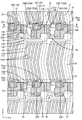
画素電極17は、図2に示すように、一対ずつのゲート配線18及びソース配線19により囲まれた縦長の概ね方形の領域に配されており、その長辺部分がソース配線19に並行してジグザグ状をなしている。画素電極17には、自身の長辺部分に沿って延在する複数(図2では4本)のスリット17A1が開口形成されている。アレイ基板11Bの表示領域AAの内面側には、画素電極17と重畳する形で概ねベタ状の共通電極20が形成されている。共通電極20の詳しい構成については後に改めて説明する。互いに重畳する画素電極17と共通電極20との間に電位差が生じると、後述する液晶層11Cには、アレイ基板11Bの板面に沿う成分に加えて、アレイ基板11Bの板面に対する法線方向の成分を含むフリンジ電界(斜め電界)がスリット17A1付近に印加される。つまり、本実施形態に係る液晶パネル11は、動作モードがFFS(Fringe Field Switching)モードとされる。さらには、画素電極17をY軸方向について両側から挟み込む一対のゲート配線18の間となる位置には、複数ずつの画素電極17及びソース配線19を横切る形でゲート配線18に並行する容量配線21が設けられている。容量配線21は、画素電極17及びソース配線19とは異なる層に配されるとともに画素電極17の一部と重畳しており、画素電極17との間で静電容量を形成している。この容量配線21により、TFT16の駆動に伴って充電された画素電極17の電位を一定期間保持することが可能とされる。容量配線21は、ゲート配線18と同層に配されている。好ましくは、容量配線21は、共通電極20と同電位とされるが、必ずしもその限りではない。
As shown in FIG. 2, the
より詳しくは、TFT16は、図3に示すように、接続対象とされる画素電極17に対してY軸方向について図3に示す下側に隣り合う配置とされる。TFT16を構成するゲート電極16Aは、ゲート配線18から分岐されており、ゲート配線18からY軸方向に沿って画素電極17側に突出している。TFT16を構成するソース電極16Bは、ソース配線19から分岐されており、ソース配線19からX軸方向に沿ってゲート電極16A側に突出するとともにその突出先端部がゲート電極16Aと重畳している。TFT16を構成するドレイン電極16Cは、ソース電極16Bに対してX軸方向について間隔を空けて配されるとともにその一部がゲート電極16Aと重畳している。ドレイン電極16Cは、ソース電極16Bと同層に配されている。ドレイン電極16Cには、次述するドレイン配線(画素電極接続配線)22の一端側が接続されている。TFT16を構成するチャネル部16Dは、後述するゲート絶縁膜26を介してゲート電極16Aと重畳するとともに、ソース電極16B及びドレイン電極16Cにそれぞれ接続されている。チャネル部16Dは、ゲート電極16Aを横切りつつX軸方向に沿って延在し、その一端側がソース電極16Bに、他端側がドレイン電極16Cに、それぞれ接続されている。
More specifically, as shown in FIG. 3, the
ドレイン配線22に関して詳しく説明する。ドレイン配線22は、ドレイン電極16Cと同層に配されており、図3に示すように、ドレイン電極16C側とは反対側の他端側が画素電極17に接続されている。より詳しくは、ドレイン配線22は、ドレイン電極16CからX軸方向に沿ってソース電極16B側とは反対側(図3に示す右側)に向けて延出する第1配線部22Aと、第1配線部22Aから屈曲されてY軸方向に沿って画素電極17側(図3に示す上側)に向けて延出する第2配線部22Bと、第2配線部22Bの延出先端部であって画素電極17に接続される電極接続部22Cと、を有する。さらには、ドレイン配線22は、第2配線部22Bの電極接続部22Cにて再び屈曲されてX軸方向に沿ってTFT16の接続対象となるソース配線19側(図3に示す左側)に向けて延出する第3配線部22Dを有する。このように、ドレイン配線22は、全体として平面に視て折り返し状をなしている。このドレイン配線22の接続対象である画素電極17は、既述したスリット17A1が形成される電極本体17Aと、電極本体17AからY軸方向に沿ってTFT16側に向けて突出してドレイン配線22に接続されるドレイン配線接続部(接続箇所)17Bと、を有する。互いに接続されるドレイン配線接続部17B及び電極接続部22Cは、Y軸方向について容量配線21と第2配線部22Bとの間となる位置に配されている。ドレイン配線接続部17B及び電極接続部22Cは、画素電極17をX軸方向について両側から挟み込む一対のソース配線19の間の中間位置に対してX軸方向について偏在しており、具体的には図3に示す右側のソース配線19寄りの配置となっている。つまり、画素電極17を挟み込む一対のソース配線19には、ドレイン配線接続部17B及び電極接続部22Cとの間の距離が相対的に短い第1ソース配線(第1信号配線)19αと、ドレイン配線接続部17B及び電極接続部22Cとの間の距離が相対的に長い第2ソース配線(第2信号配線)19βと、が含まれている、と言える。なお、以下の説明及び図3では、画素電極17を挟み込む一対のソース配線19を、ドレイン配線接続部17B及び電極接続部22Cとの間の距離に応じて区別しており、具体的には、上記距離が相対的に短いものを第1ソース配線として符号に添え字「α」を付すのに対し、上記距離が相対的に長いものを第2ソース配線として符号に添え字「β」を付している。第1ソース配線19αは、第2ソース配線19βに比べると、ドレイン配線接続部17B及び電極接続部22Cに対して近い配置とされる。第1ソース配線19αに比べてドレイン配線接続部17B及び電極接続部22Cから遠い配置の第2ソース配線19βには、ソース電極16Bが設けられている。つまり、画素電極17を挟み込む一対のソース配線19のうちの第2ソース配線19βが上記画素電極17の接続対象とされており、第1ソース配線19αは、上記画素電極17の接続対象外であり、上記画素電極17に対して図3に示す右側に隣り合う画素電極17の接続対象とされる。
The
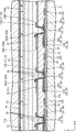
液晶パネル11を構成する両基板11A,11B間には、図4に示すように、電界印加に伴って光学特性が変化する物質である液晶分子を含む図示しない液晶層11Cが設けられている。液晶層11Cを介してアレイ基板11Bと対向状をなすCF基板11Aの表示領域AAにおける内面側には、アレイ基板11B側の各画素電極17と対向状をなす位置に多数個のカラーフィルタ23がマトリクス状に並んで設けられている。カラーフィルタ23は、R(赤色),G(緑色),B(青色)の三色が所定の順で繰り返し並んで配されてなる。また、各カラーフィルタ23間には、混色を防ぐための遮光部(ブラックマトリクス)24が形成されている。なお、両基板11A,11Bにおける液晶層11C側の最内面には、液晶層11Cに含まれる液晶分子の配向を規制するための配向膜(図示せず)がそれぞれ設けられている。
As shown in FIG. 4, a liquid crystal layer 11C (not shown) containing liquid crystal molecules, which is a substance whose optical characteristics change with application of an electric field, is provided between the two
続いて、アレイ基板11Bの内面側に積層形成された各種の膜について説明する。アレイ基板11Bには、図4に示すように、下層側から順に第1金属膜(ゲート金属膜)25、ゲート絶縁膜26、半導体膜27、第2金属膜(ソース金属膜)28、第1層間絶縁膜29、平坦化膜30、第1透明電極膜31、第2層間絶縁膜32、第2透明電極膜33が積層形成されている。
Subsequently, various films laminated and formed on the inner surface side of the
第1金属膜25は、異なる種類の金属材料を積層してなる積層膜または1種類の金属材料からなる単層膜とされ、図3及び図4に示すように、ゲート配線18及び容量配線21やTFT16のゲート電極16Aや予備配線などを構成する。ゲート絶縁膜26は、SiNxやSiO2などの無機絶縁材料(無機材料)からなる。半導体膜27は、材料として例えば酸化物半導体を用いた薄膜からなり、TFT16を構成するチャネル部16Dなどを構成する。第2金属膜28は、第1金属膜25と同様に、積層膜または単層膜とされ、ソース配線19及びドレイン配線22やTFT16のソース電極16B及びドレイン電極16Cなどを構成する。第1層間絶縁膜29は、ゲート絶縁膜26と同様に無機絶縁材料からなる。平坦化膜30は、例えばPMMA(アクリル樹脂)などの有機絶縁材料(有機材料)からなり、その膜厚が無機樹脂材料からなる他の絶縁膜26,29,32よりも大きい。この平坦化膜30によりアレイ基板11Bの表面が平坦化される。第1透明電極膜31は、例えばITOなどの透明電極材料からなり、共通電極20を構成する。第2層間絶縁膜32は、ゲート絶縁膜26などと同様に無機絶縁材料からなる。第2透明電極膜33は、第1透明電極膜31と同様に透明電極材料からなり、画素電極17を構成する。第1層間絶縁膜29、平坦化膜30及び第2層間絶縁膜32には、第2透明電極膜33からなる画素電極17を第2金属膜28からなるドレイン配線22に接続するためのコンタクトホールCHが開口形成されている。コンタクトホールCHは、画素電極17のドレイン配線接続部17Bと、ドレイン配線22の電極接続部22Cと、の双方と平面に視て重畳する位置に配されている。このコンタクトホールCHを除いて第1層間絶縁膜29、平坦化膜30及び第2層間絶縁膜32は、少なくとも表示領域AAの全域にわたってベタ状に形成されている。
The
ところで、共通電極20には、図2に示すように、少なくともソース配線19と画素電極17におけるドレイン配線接続部17Bとに跨る範囲の開口部20Aが設けられている。なお、図2及び図3では、開口部20Aの形成範囲を、後述する遮蔽部34とは異なる網掛け状にして図示している。本実施形態に係る開口部20Aは、ソース配線19及び画素電極17におけるドレイン配線接続部17Bに加えてドレイン配線22に跨る範囲を有している。詳しくは、開口部20Aは、図3に示すように、第1ソース配線19αと重畳し且つX軸方向について第1ソース配線19αの両側方領域に広がる範囲の第1開口部20A1と、ドレイン配線22と重畳し且つX軸方向についてドレイン配線22の両側方領域に広がる範囲の第2開口部20A2と、ドレイン配線接続部17B、電極接続部22C及びコンタクトホールCHと重畳する範囲の第3開口部20A3と、を相互に連ねた構成とされる。このうち、第3開口部20A3は、共通電極20よりも上層側に配された画素電極17のドレイン配線接続部17Bが、共通電極20よりも下層側に配されたドレイン配線22の電極接続部22Cに達するようコンタクトホールCHに通される途中で共通電極20と短絡するのを防ぐためのものである。第1開口部20A1及び第2開口部20A2は、修理に際してソース配線19やドレイン配線22にレーザ光を照射した場合に、ソース配線19やドレイン配線22が共通電極20と短絡するのを防ぐためのものである。
By the way, as shown in FIG. 2, the
具体的には、例えば第1ソース配線19αがゲート配線18と短絡する不具合が生じた場合には、上記した第1開口部20A1を通して第1ソース配線19αにレーザ光を照射し、第1ソース配線19αを切断するとともに、その第1ソース配線19αを予備配線に接続するようにして修理を行う。この修理により、第1ソース配線19αに接続された各TFT16に、予備配線を経由して画像信号を供給することができる。このとき、第1開口部20A1は、第1ソース配線19αとその両側方領域に広がっているので、第1ソース配線19αにおけるレーザ光の照射箇所が共通電極20と短絡する事態が生じるのが回避される。また、例えばゲート配線18とドレイン配線22とが短絡したり、ゲート電極16Aとドレイン電極16Cとが短絡したりする不具合が生じた場合には、上記した第2開口部20A2を通してドレイン配線22の第2配線部22Bにレーザ光を照射し、第2配線部22Bを切断するとともに、容量配線21を画素電極17に短絡させるようにして修理を行う。この修理により、ゲート配線18(ゲート電極16A)とドレイン配線22(ドレイン電極16C)との短絡に起因して輝点化する画素を黒点化することができる。このとき、第2開口部20A2は、ドレイン配線22とその両側方領域に広がっているので、ドレイン配線22におけるレーザ光の照射箇所が共通電極20と短絡する事態が生じるのが回避される。その一方、共通電極20が上記のような開口部20Aを有する構成とされると、第1ソース配線19αと画素電極17におけるドレイン配線接続部17Bとの間には、共通電極20が非配置となるため、第1ソース配線19αとドレイン配線接続部17Bとの間に電界が生じ易くなる。このため、第1ソース配線19αとドレイン配線接続部17Bとの間の電界により生じる寄生容量に起因して表示品位が低下することが懸念される。
Specifically, for example, when the first source wiring 19α has a short circuit with the
そこで、本実施形態に係るアレイ基板11Bには、図3及び図5に示すように、ソース配線19と画素電極17におけるドレイン配線22に対するドレイン配線接続部17Bとの間となる位置に配されて両者17B,19間の電界を遮蔽する遮蔽部34が設けられている。遮蔽部34は、ゲート配線18及び容量配線21と同じ第1金属膜25からなり、容量配線21に連ねられている。なお、図3では、遮蔽部34及び遮蔽部34に連なる容量配線21の形成範囲を、開口部20Aとは異なる網掛け状にして図示している。このように、ソース配線19と画素電極17のドレイン配線接続部17Bとの間となる位置に配される遮蔽部34により両者17B,19の間に生じる電界を遮蔽することができる。これにより、ソース配線19と画素電極17におけるドレイン配線接続部17Bとの間の電界により生じる寄生容量が抑制され、もって表示品位の低下が抑制される。その上、遮蔽部34は、共通電極20と同電位とされる容量配線21に接続されているので、十分な遮蔽効果を発揮することができる。しかも、容量配線21は、例えば走査信号を伝送するゲート配線18に比べると、低電位に保たれているから、遮蔽部34の遮蔽性能が安定化し、高い信頼性が得られる。
Therefore, as shown in FIGS. 3 and 5, the
遮蔽部34は、図3及び図5に示すように、画素電極17を挟み込む一対のソース配線19と、画素電極17におけるドレイン配線接続部17Bと、の間となる位置にそれぞれ配されている。遮蔽部34は、各ドレイン配線接続部17BをX軸方向について両側から挟み込む形で一対ずつ配されている。ドレイン配線接続部17Bを挟み込む一対の遮蔽部34αは、容量配線21からY軸方向に沿ってゲート配線18側に向けて突出しており、平面形状が略方形とされる。容量配線21には、各画素電極17に対して一対ずつ配された遮蔽部34がそれぞれ連ねられている。ドレイン配線接続部17Bを挟み込む一対の遮蔽部34には、開口部20Aの少なくとも一部と重畳するよう配される開口重畳遮蔽部34αと、開口部20Aとは非重畳となるよう配される開口非重畳遮蔽部34βと、が含まれている。なお、以下の説明では、ドレイン配線接続部17Bを挟み込む一対の遮蔽部34を区別する場合には、開口部20Aと重畳するものを開口重畳遮蔽部として符号に添え字「α」を付すのに対し、開口部20Aと重畳しないものを開口非重畳遮蔽部として符号に添え字「β」を付している。
As shown in FIG. 3 and FIG. 5, the shielding
開口重畳遮蔽部34αは、図3及び図5に示すように、開口部20Aのうちの第1開口部20A1と第3開口部20A3とに跨る範囲に配されている。つまり、開口重畳遮蔽部34αは、一対のソース配線19のうちのドレイン配線接続部17Bとの間の距離が短い第1ソース配線19αとドレイン配線接続部17Bとの間となる位置に配されている。ここで、上記距離が短い第1ソース配線19αは、同距離が長い第2ソース配線19βに比べると、画素電極17におけるドレイン配線接続部17Bとの間に生じる電界が強く、寄生容量が大きくなる傾向にある。しかも、共通電極20の開口部20Aが第1ソース配線19αと画素電極17におけるドレイン配線接続部17Bとに跨る範囲とされているため、第1ソース配線19αと画素電極17におけるドレイン配線接続部17Bとの間に電界がより生じ易くなっている。その点、開口重畳遮蔽部34αは、第1ソース配線19αと画素電極17におけるドレイン配線接続部17Bとの間となる位置に配されているので、電界を効率的に遮蔽することができる。これにより、寄生容量を効率的に低下させることができ、もってソース配線19の修正を可能としつつ表示品位の低下が好適に抑制される。また、開口重畳遮蔽部34αは、画素電極17のドレイン配線接続部17B及びドレイン配線22の電極接続部22Cの一部ずつと重畳するよう配されている。このようにすれば、開口重畳遮蔽部34αと、画素電極17におけるドレイン配線接続部17Bの一部及びドレイン配線22の一部と、の間にそれぞれ電界が生じることで、第1ソース配線19αと画素電極17におけるドレイン配線接続部17Bとの間に生じる電界をより効率的に遮蔽することができる。これにより、表示品位の低下がより好適に抑制される。
As shown in FIGS. 3 and 5, the opening overlapping shielding portion 34α is disposed in a range extending over the first opening 20A1 and the third opening 20A3 of the
開口非重畳遮蔽部34βは、図3及び図5に示すように、一対のソース配線19のうちのドレイン配線接続部17Bとの間の距離が長い第2ソース配線19βとドレイン配線接続部17Bとの間となる位置に配されている。開口非重畳遮蔽部34βは、その大部分がドレイン配線22における第3配線部22Dと重畳する配置とされる。一方、開口非重畳遮蔽部34βは、画素電極17におけるドレイン配線接続部17Bとは非重畳の配置とされる。開口非重畳遮蔽部34βは、開口部20Aとは非重畳の配置とされているものの、上記のように第2ソース配線19βとドレイン配線接続部17Bとの間となる位置に配されることで、第2ソース配線19βとドレイン配線接続部17Bとの間に生じる電界を遮蔽することができる。これにより、表示品位の低下がより好適に抑制される。しかも、既述した通り、開口重畳遮蔽部34α及び開口非重畳遮蔽部34βは、画素電極17におけるドレイン配線接続部17Bを挟み込むよう配されているので、画素電極17を挟み込むよう配される一対のソース配線19と画素電極17におけるドレイン配線接続部17Bとの間に生じる各電界を、開口重畳遮蔽部34α及び開口非重畳遮蔽部34βによってそれぞれ遮蔽することができる。これにより、表示品位の低下がさらに好適に抑制される。
The opening non-overlapping shielding portion 34β is, as shown in FIGS. 3 and 5, the second source wiring 19β and the drain
ここで、各ソース配線19と画素電極17におけるドレイン配線接続部17Bとの間にそれぞれ生じる寄生容量が、開口非重畳遮蔽部34βの有無に応じてどのように変化するかに関して知見を得るべく、以下の比較実験を行った。この比較実験では、開口重畳遮蔽部34αについては形成するものの開口非重畳遮蔽部34βを非形成とした構成の比較例と、開口重畳遮蔽部34α及び開口非重畳遮蔽部34βを両方とも形成した構成の実施例と、を用いている。比較例は、開口非重畳遮蔽部34βが非形成とされる点を除いて、本段落以前に説明した液晶パネル11と同様の構成である。実施例は、本段落以前に説明した液晶パネル11と同様の構成である。比較実験では、上記した比較例及び実施例に関し、第1ソース配線19αとドレイン配線接続部17Bとの間に生じる寄生容量Csd1と、第2ソース配線19βとドレイン配線接続部17Bとの間に生じる寄生容量Csd2と、をそれぞれ測定しており、その結果は図6に示す通りである。図6の表には、比較例及び実施例における各寄生容量Csd1,Csd2の値(単位は「pF」)と、各寄生容量Csd1,Csd2に関する比較例と実施例との差分の値(単位は「pF」)と、上記差分の値を比較例における各寄生容量Csd1,Csd2の値にて除して算出した改善率(単位は「%」)と、が示されている。
Here, in order to obtain knowledge as to how the parasitic capacitance generated between each
比較実験の実験結果について説明する。図6によれば、まず、比較例及び実施例のいずれにおいても寄生容量Csd1の値が寄生容量Csd2の値よりも大きい。これは、第1ソース配線19αが第2ソース配線19βよりもドレイン配線接続部17Bの近くに配されているため、第1ソース配線19αとドレイン配線接続部17Bとの間に生じる電界が、第2ソース配線19βとドレイン配線接続部17Bとの間に生じる電界よりも強い結果と推考される。次に、実施例は、比較例よりも各寄生容量Csd1,Csd2の値がそれぞれ低下しており、寄生容量Csd1に関する比較例と実施例との差分の値(0.000158pF)が寄生容量Csd2に関する比較例と実施例との差分の値(0.000018pF)よりも大きくなっているとともに、寄生容量Csd1の改善率(27.0%)が寄生容量Csd2の改善率(7.6%)よりも高くなっている。これは、実施例に備わる開口重畳遮蔽部34αは、第1ソース配線19αとドレイン配線接続部17Bとの間となる配置とされているので、第1ソース配線19αとドレイン配線接続部17Bとの間に生じる電界が開口重畳遮蔽部34αによって効率的に遮蔽された結果と推考される。続いて、実施例における寄生容量Csd1と寄生容量Csd2との差分の値(0.000210pF)は、比較例における寄生容量Csd1と寄生容量Csd2との差分の値(0.000350pF)よりも小さくなっている。この結果は、上記した改善率の値の差に因るものと推考される。ここで、表示品位の判定に際しては、寄生容量Csd1と寄生容量Csd2との差分の絶対値を、画素に関わる全ての静電容量の和(具体的には、画素電極17と共通電極20との間の静電容量Clc(液晶容量)と、画素電極17と容量配線21との間の静電容量と、ゲート配線18とドレイン配線22との間の寄生容量と、上記寄生容量Csd1と、上記寄生容量Csd2と、の和)にて除した値を算出し、その値が所定の判定基準値以下であれば、表示品位が良好と判定し、判定基準値を上回れば、表示品位が芳しくないと判定している。実施例は、比較例よりも寄生容量Csd1と寄生容量Csd2との差分の絶対値が小さいので、上記した算出値が判定基準値以下となり易くなっている。これにより、実施例によれば比較例よりも高い表示品位が得られる、と言える。より具体的には、上記した画素に関わる全ての静電容量の和の数値が例えば0.528pFとされる場合には、寄生容量Csd1と寄生容量Csd2との差分の絶対値を画素に関わる全ての静電容量の和にて除した値は、それぞれ比較例が0.000663、実施例が0.000398となる。そして、判定基準値が0.0004とされる場合は、比較例が判定基準値を上回り、実施例が判定基準値を下回ることになる。従って、実施例は比較例よりも表示品位が優れたものとなる。
The experimental results of the comparative experiment will be described. According to FIG. 6, first of all, the value of the parasitic capacitance Csd1 is larger than the value of the parasitic capacitance Csd2 in both the comparative example and the example. Since the first source wiring 19α is disposed closer to the
以上説明したように本実施形態の液晶表示装置(表示装置)10は、画素電極17と、画素電極17に供給する信号を伝送するソース配線(信号配線)19と、ソース配線19に対して間隔を空けた位置に配されて画素電極17に接続されるドレイン配線(画素電極接続配線)22と、ソース配線19と、画素電極17におけるドレイン配線22に対するドレイン配線接続部(接続箇所)17Bと、の間となる位置に配されて両者17B,19間の電界を遮蔽する遮蔽部34と、を備える。
As described above, in the liquid crystal display device (display device) 10 according to the present embodiment, the
このようにすれば、画素電極17には、ソース配線19に伝送される信号に基づく電位がドレイン配線22を介して供給される。遮蔽部34は、ソース配線19と、画素電極17におけるドレイン配線22に対するドレイン配線接続部17Bと、の間となる位置に配されていて、両者17B,19の間に生じる電界を遮蔽する。これにより、ソース配線19と画素電極17におけるドレイン配線接続部17Bとの間の電界により生じる寄生容量が抑制され、もって表示品位の低下が抑制される。
In this way, the potential based on the signal transmitted to the
また、画素電極17、ソース配線19及びドレイン配線22とは異なる層にて少なくとも画素電極17と重畳するよう配される共通電極20であって、少なくともソース配線19と画素電極17におけるドレイン配線接続部17Bとに跨る範囲の開口部20Aを有する共通電極20を備えており、遮蔽部34には、開口部20Aの少なくとも一部と重畳するよう配される開口重畳遮蔽部34αが含まれる。このようにすれば、画素電極17が充電されると、画素電極17と共通電極20との間に生じる電位差を利用して画像が表示される。共通電極20は、少なくともソース配線19と画素電極17におけるドレイン配線接続部17Bとに跨る範囲の開口部20Aを有しているので、例えばソース配線19の修理を行う際に、修理に伴ってソース配線19が共通電極20と短絡する事態を防ぐことができる。しかしながら、共通電極20が上記のような開口部20Aを有する構成とされると、ソース配線19と画素電極17におけるドレイン配線接続部17Bとの間に電界が生じ易くなるため、その電界により生じる寄生容量に起因して表示品位が低下することが懸念される。その点、遮蔽部34には、ソース配線19と画素電極17におけるドレイン配線接続部17Bとの間となる位置にて共通電極20の開口部20Aの少なくとも一部と重畳する開口重畳遮蔽部34αが含まれているから、ソース配線19と画素電極17におけるドレイン配線接続部17Bとの間に生じる電界を開口重畳遮蔽部34αにより効率的に遮蔽することができる。これにより、ソース配線19と画素電極17におけるドレイン配線接続部17Bとの間の電界により生じる寄生容量が効率的に抑制され、もってソース配線19の修正を可能としつつ表示品位の低下が好適に抑制される。
The
また、遮蔽部34には、開口部20Aとは非重畳となるよう配される開口非重畳遮蔽部34βが含まれる。このようにすれば、遮蔽部34には、ソース配線19と画素電極17におけるドレイン配線接続部17Bとの間となる位置にて共通電極20の開口部20Aの少なくとも一部と重畳する開口重畳遮蔽部34αに加えて、ソース配線19と画素電極17におけるドレイン配線接続部17Bとの間となる位置にて共通電極20の開口部20Aとは非重畳となる開口非重畳遮蔽部34βが含まれているから、ソース配線19と画素電極17におけるドレイン配線接続部17Bとの間に生じる電界をさらに遮蔽することができる。これにより、表示品位の低下がより好適に抑制される。
In addition, the shielding
また、ソース配線19は、画素電極17を挟み込むよう一対配されており、開口重畳遮蔽部34α及び開口非重畳遮蔽部34βは、画素電極17におけるドレイン配線接続部17Bを挟み込むよう配される。このようにすれば、画素電極17を挟み込むよう配される一対のソース配線19と画素電極17におけるドレイン配線接続部17Bとの間に生じる各電界を、画素電極17におけるドレイン配線接続部17Bを挟み込むよう配される開口重畳遮蔽部34α及び開口非重畳遮蔽部34βによってそれぞれ遮蔽することができる。これにより、表示品位の低下がさらに好適に抑制される。
Further, the
また、ソース配線19は、画素電極17を挟み込むとともにドレイン配線接続部17Bとの間の距離が異なるよう一対配されており、共通電極20は、開口部20Aが、少なくともドレイン配線接続部17Bとの間の距離が短いソース配線19である第1ソース配線(第1信号配線)19とドレイン配線接続部17Bとに跨る範囲とされており、開口重畳遮蔽部34αは、一対のソース配線19のうちのドレイン配線接続部17Bとの間の距離が短いソース配線19である第1ソース配線19αとドレイン配線接続部17Bとの間となる位置に配されている。このようにすれば、共通電極20の開口部20Aが、少なくとも画素電極17におけるドレイン配線接続部17Bとの間の距離が短いソース配線19である第1ソース配線19αと画素電極17におけるドレイン配線接続部17Bとに跨る範囲とされているので、ドレイン配線接続部17Bとの間の距離が短いソース配線19である第1ソース配線19αの修理を行う上で好適となる。ここで、一対のソース配線19のうちの画素電極17におけるドレイン配線接続部17Bとの間の距離が短いソース配線19である第1ソース配線19αは、同距離が長いソース配線19である第2ソース配線19βに比べると、画素電極17におけるドレイン配線接続部17Bとの間に生じる電界が強く、寄生容量が大きくなる傾向にある。しかも、共通電極20の開口部20Aが上記のような範囲とされているため、ドレイン配線接続部17Bとの間の距離が短いソース配線19である第1ソース配線19αと、画素電極17におけるドレイン配線接続部17Bと、の間に電界がより生じ易くなっている。その点、開口重畳遮蔽部34αは、一対のソース配線19のうちのドレイン配線接続部17Bとの間の距離が短いソース配線19である第1ソース配線19αと、画素電極17におけるドレイン配線接続部17Bと、の間となる位置に配されているので、電界を効率的に遮蔽することができる。これにより、寄生容量を効率的に低下させることができ、もって表示品位の低下が好適に抑制される。
Also, the
また、開口重畳遮蔽部34αは、画素電極17におけるドレイン配線接続部17Bの少なくとも一部と、ドレイン配線22の少なくとも一部と、にそれぞれ重畳するよう配される。このようにすれば、開口重畳遮蔽部34αと、画素電極17におけるドレイン配線接続部17Bの少なくとも一部、及びドレイン配線22の少なくとも一部と、の間にそれぞれ電界が生じることで、ソース配線19と画素電極17におけるドレイン配線接続部17Bとの間に生じる電界をより効率的に遮蔽することができる。これにより、表示品位の低下がより好適に抑制される。
In addition, the opening overlapping shielding portion 34α is disposed so as to overlap at least a portion of the drain
また、共通電極20は、開口部20Aがソース配線19及び画素電極17におけるドレイン配線接続部17Bに加えてドレイン配線22にわたる範囲とされる。このようにすれば、共通電極20は、ソース配線19及び画素電極17におけるドレイン配線接続部17Bに加えてドレイン配線22にわたる範囲の開口部20Aを有しているので、例えばドレイン配線22の修理を行う際に、修理に伴ってドレイン配線22が共通電極20と短絡する事態を防ぐことができる。このような範囲の開口部20Aにより、ソース配線19と画素電極17におけるドレイン配線接続部17Bとの間に生じる電界がより生じ易くなるものの、遮蔽部34によって上記電界を遮蔽することで、表示品位の低下がより好適に抑制される。
In addition to the
また、ソース配線19と交差する形で延在し、画素電極17及びソース配線19とは異なる層にて画素電極17の一部と重畳するよう配される容量配線21を備えており、遮蔽部34は、容量配線21に接続されている。このようにすれば、画素電極17は、異なる層に配されてその一部と重畳する容量配線21との間で静電容量を形成することで、ソース配線19及びドレイン配線22によって供給された電位が保持される。遮蔽部34は、容量配線21に接続されることで、十分な遮蔽効果を発揮することができる。しかも、容量配線21は、他の表示のための信号を伝送する配線に比べると、低電位に保たれているから、遮蔽部34の遮蔽性能が安定化し、高い信頼性が得られる。
In addition, a
<実施形態2>
本発明の実施形態2を図7によって説明する。この実施形態2では、共通電極120の開口部120Aの形成範囲を変更したものを示す。なお、上記した実施形態1と同様の構造、作用及び効果について重複する説明は省略する。
Second Embodiment
Embodiment 2 of the present invention will be described with reference to FIG. In the second embodiment, the range in which the
本実施形態に係る共通電極120は、図7に示すように、第1ソース配線119αと画素電極117におけるドレイン配線接続部117Bとに跨っているものの、ドレイン配線122の第2配線部122Bの大部分には至らない範囲の開口部120Aを有している。つまり、開口部120Aは、第1開口部120A1及び第3開口部120A2を有しているものの、上記した実施形態1に記載した第2開口部20A2を有さない構成とされる。このような構成であっても、上記した実施形態1と同様に遮蔽部134による寄生容量の低減効果を十分に得ることができる。なお、本実施形態は、ソース配線119の修理は可能であるものの、ドレイン配線122の修理については行うことを想定していない場合に有用である。
The
<実施形態3>
本発明の実施形態3を図8によって説明する。この実施形態3では、上記した実施形態1から開口重畳遮蔽部234αを変更したものを示す。なお、上記した実施形態1と同様の構造、作用及び効果について重複する説明は省略する。
Embodiment 3
Embodiment 3 of the present invention will be described with reference to FIG. In this third embodiment, the one in which the aperture overlapping shielding part 234α is changed from the first embodiment described above is shown. In addition, the description which overlaps about the structure similar to Embodiment 1 mentioned above, an effect | action, and an effect is abbreviate | omitted.
本実施形態に係る遮蔽部234には、図8に示すように、上記した実施形態1と同様に容量配線221に連なる開口非重畳遮蔽部234βと、ゲート配線218に連なる開口重畳遮蔽部234αと、が含まれている。なお、図8では、遮蔽部234及び遮蔽部234に連なるゲート配線218(ゲート電極216Aを含む)及び容量配線221の形成範囲を、開口部220Aとは異なる網掛け状にして図示している。開口重畳遮蔽部234αは、ゲート配線218と同じ第1金属膜からなる。開口重畳遮蔽部234αは、ゲート配線218からY軸方向に沿ってゲート電極216Aと同じ側に突出し、第1ソース配線219αと画素電極217におけるドレイン配線接続部217Bとの間となる位置に配されている。開口重畳遮蔽部234αは、共通電極220の開口部220Aのうちの第1開口部220A1、第2開口部220A2及び第3開口部220A3の全てに対して重畳するよう配されている。このような開口重畳遮蔽部234αによっても、寄生容量の低減効果を十分に得ることができる。
In the shielding
<他の実施形態>
本発明は上記記述及び図面によって説明した実施形態に限定されるものではなく、例えば次のような実施形態も本発明の技術的範囲に含まれる。
(1)上記した各実施形態では、開口重畳遮蔽部及び開口非重畳遮蔽部がドレイン配線の一部ずつと重畳する配置を示したが、開口重畳遮蔽部及び開口非重畳遮蔽部のいずれかまたは両方がドレイン配線とは非重畳の配置であっても構わない。例えば、ドレイン配線の第3配線部を省略すれば、開口非重畳遮蔽部がドレイン配線とは非重畳の配置となる。
(2)上記した各実施形態では、開口重畳遮蔽部がドレイン配線のうちの電極接続部のみと重畳する配置を示したが、開口重畳遮蔽部がドレイン配線における電極接続部以外の部分と重畳していてもよい。例えば、開口重畳遮蔽部が電極接続部に加えて第2配線部と重畳する配置であっても構わない。
(3)上記した各実施形態では、開口重畳遮蔽部が画素電極のドレイン配線接続部と重畳する配置を示したが、開口重畳遮蔽部が画素電極のドレイン配線接続部とは非重畳の配置であっても構わない。
(4)上記した実施形態1では、開口重畳遮蔽部が開口部のうちの第1開口部及び第2開口部と重畳し、第3開口部とは非重畳とされる配置を示したが、開口重畳遮蔽部が第1開口部及び第2開口部に加えて第3開口部とも重畳する配置であっても構わない。逆に、開口重畳遮蔽部が第1開口部のみと重畳し、第2開口部及び第3開口部とは非重畳とされる配置であっても構わない。
(5)上記した各実施形態では、画素電極のドレイン配線接続部を挟み込む一対の遮蔽部が開口重畳遮蔽部及び開口非重畳遮蔽部とされる場合を示したが、画素電極のドレイン配線接続部を挟み込む一対の遮蔽部がいずれも開口重畳遮蔽部とされる構成や上記一対の遮蔽部がいずれも開口非重畳遮蔽部とされる構成であっても構わない。いずれの場合であっても、ドレイン配線接続部が一対の遮蔽部によって挟み込まれる構成となるので、画素電極を挟み込む一対のソース配線とドレイン配線接続部との間に生じる電界を一対の遮蔽部によって遮蔽することができ、十分な寄生容量低減効果を得ることができる。
(6)上記した各実施形態以外にも、共通電極における開口部の形成範囲や平面配置、開口重畳遮蔽部の形成範囲や平面配置、開口非重畳遮蔽部の形成範囲や平面配置、共通電極の開口部に対する開口重畳遮蔽部の重畳範囲や平面配置などは、適宜に変更可能である。
(7)上記した各実施形態では、画素電極のドレイン配線接続部を挟み込む形で一対の遮蔽部が設けられた場合を示したが、いずれか一方の遮蔽部(開口重畳遮蔽部または開口非重畳遮蔽部)を省略することも可能である。
(8)上記した各実施形態では、画素電極を挟み込む一対のソース配線と、ドレイン配線接続部と、の間の距離が異なる場合を示したが、上記距離が等しくなる構成であっても構わない。
(9)上記した各実施形態では、マトリクス状に平面配置された各画素電極におけるドレイン配線接続部が全て同じ側(図3などの右側)に偏在する場合を示したが、ドレイン配線接続部が一方側(例えば図3などの右側)に偏在する行と、ドレイン配線接続部が他方側(例えば図3などの左側)に偏在する行と、が交互に繰り返し並ぶ配列を採ることも可能である。その場合は、開口重畳遮蔽部及び開口非重畳遮蔽部が行毎に左右反転した配置とするのが好ましい。
(10)上記した各実施形態では、遮蔽部が容量配線やゲート配線と同層で且つ同一材料(第1金属膜)からなる場合を示したが、遮蔽部を容量配線やゲート配線とは異なる層に配置しつつも容量配線やゲート配線に対して接続することも可能である。その場合は、遮蔽部と容量配線やゲート配線との間に介在する絶縁膜にコンタクトホールを開口形成すればよい。
(11)上記した各実施形態では、遮蔽部が容量配線やゲート配線に接続される場合を示したが、遮蔽部を他の配線や電極に接続することも可能である。
(12)上記した各実施形態では、各絶縁膜に連通するコンタクトホールの形成範囲や平面形状を簡略化して図示したが、各絶縁膜のコンタクトホールの形成範囲や平面形状は適宜に変更可能であり、また各絶縁膜毎にコンタクトホールの形成範囲や平面形状を互いに異ならせることも可能である。
(13)上記した各実施形態では、画素電極が相対的に上層側に、共通電極が相対的に下層側に、それぞれ配された場合を示したが、画素電極を相対的に下層側に、共通電極を相対的に上層側に、それぞれ配置することも可能である。その場合は、共通電極の開口部から第3開口部を省略することが可能である。
(14)上記した各実施形態では、平面形状が長方形とされる液晶パネルについて示したが、平面形状が正方形、円形、楕円形などとされる液晶パネルにも本発明は適用可能である。
(15)上記した各実施形態では、ドライバが液晶パネルのアレイ基板に対してCOG実装される場合を例示したが、ドライバがフレキシブル基板に対してCOF(Chip On Film)実装される構成であってもよい。
(16)上記した各実施形態では、TFTのチャネル部を構成する半導体膜が酸化物半導体材料からなる場合を例示したが、それ以外にも、例えばポリシリコン(多結晶化されたシリコン(多結晶シリコン)の一種であるCGシリコン(Continuous Grain Silicon))やアモルファスシリコンを半導体膜の材料として用いることも可能である。
(17)上記した各実施形態では、液晶パネルのカラーフィルタが赤色、緑色及び青色の3色構成とされたものを例示したが、赤色、緑色及び青色の各着色部に、黄色の着色部を加えて4色構成としたカラーフィルタを備えたものにも本発明は適用可能である。
(18)上記した各実施形態では、一対の基板間に液晶層が挟持された構成とされる液晶パネル及びその製造方法について例示したが、一対の基板間に液晶材料以外の機能性有機分子(媒質層)を挟持した表示パネルについても本発明は適用可能である。
(19)上記した各実施形態では、液晶パネルのスイッチング素子としてTFTを用いたが、TFT以外のスイッチング素子(例えば薄膜ダイオード(TFD))を用いた液晶パネルにも適用可能であり、カラー表示する液晶パネル以外にも、白黒表示する液晶パネルにも適用可能である。
(20)上記した各実施形態では、表示パネルとして液晶パネルを例示したが、他の種類の表示パネル(PDP(プラズマディスプレイパネル)、有機ELパネル、EPD(電気泳動ディスプレイパネル)、MEMS(Micro Electro Mechanical Systems)表示パネルなど)にも本発明は適用可能である。
Other Embodiments
The present invention is not limited to the embodiments described above with reference to the drawings. For example, the following embodiments are also included in the technical scope of the present invention.
(1) In each embodiment described above, the arrangement in which the opening overlapping shielding part and the opening non-overlapping shielding part overlap with each part of the drain wiring is shown, but either the opening overlapping shielding part or the opening non-overlapping shielding part Both of them may be arranged so as not to overlap with the drain wiring. For example, if the third wiring portion of the drain wiring is omitted, the non-overlapping shielding portion does not overlap the drain wiring.
(2) In each embodiment described above, the arrangement in which the opening overlapping shielding portion overlaps only with the electrode connection portion of the drain wiring is shown, but the opening overlapping shielding portion overlaps with a portion other than the electrode connection portion in the drain wiring. It may be For example, the opening superimposing shielding portion may be disposed so as to overlap with the second wiring portion in addition to the electrode connection portion.
(3) In each of the above-described embodiments, the arrangement in which the opening overlapping shielding portion overlaps the drain wiring connection portion of the pixel electrode is illustrated, but the opening overlapping shielding portion does not overlap the drain wiring connection portion of the pixel electrode. It does not matter.
(4) In the first embodiment described above, the opening overlapping shielding portion overlaps with the first opening and the second opening of the opening and does not overlap the third opening. In addition to the first opening and the second opening, the opening overlapping shielding portion may also be arranged to overlap the third opening. Conversely, the opening overlapping shielding portion may overlap only with the first opening, and the second opening and the third opening may be non-overlapping.
(5) In each embodiment described above, the case where the pair of shielding parts sandwiching the drain wiring connection part of the pixel electrode is the opening overlapping shielding part and the opening non-overlapping shielding part is shown. Either a configuration in which a pair of shielding portions sandwiching the opening is an opening overlapping shielding portion or a configuration in which both the pair of shielding portions are an opening non-overlapping shielding portion may be employed. In any case, since the drain wiring connection portion is sandwiched by the pair of shielding portions, an electric field generated between the pair of source wiring and the drain wiring connection portion sandwiching the pixel electrode is generated by the pair of shielding portions. It is possible to shield and obtain a sufficient parasitic capacitance reduction effect.
(6) In addition to the above embodiments, the formation range and the plane arrangement of the opening in the common electrode, the formation range and the plane arrangement of the opening superposition shielding unit, the formation area and the plane arrangement of the opening non-overlapping shielding unit, and the common electrode The overlapping range and planar arrangement of the opening overlapping shielding portion with respect to the opening can be changed as appropriate.
(7) In each embodiment described above, the case where the pair of shielding portions are provided to sandwich the drain wiring connection portion of the pixel electrode is shown, but any one shielding portion (opening overlapping shielding portion or opening non-overlapping is shown It is also possible to omit the shielding part).
(8) In each embodiment described above, the case where the distance between the pair of source wiring sandwiching the pixel electrode and the drain wiring connection portion is different is shown, but the distance may be equal. .
(9) In each of the above-described embodiments, the drain wiring connection portion in each pixel electrode arranged flat in a matrix is shown to be unevenly distributed on the same side (right side of FIG. 3 etc.) It is also possible to adopt an arrangement in which rows distributed unevenly on one side (for example, the right side in FIG. 3) and rows distributed unevenly on the other side (for example, the left in FIG. 3) are alternately arranged. . In such a case, it is preferable that the aperture overlapping shielding portion and the aperture non-overlapping shielding portion be arranged so as to be horizontally reversed for each row.
(10) In each embodiment described above, the case where the shielding portion is the same layer as the capacitive wiring and the gate wiring and made of the same material (first metal film) is shown, but the shielding portion is different from the capacitive wiring and the gate wiring It is also possible to connect to a capacitor wiring or a gate wiring while arranging in a layer. In that case, a contact hole may be formed in the insulating film interposed between the shielding portion and the capacitor wiring or the gate wiring.
(11) In each of the above-described embodiments, the case where the shielding portion is connected to the capacitive wiring or the gate wiring is shown, but it is also possible to connect the shielding portion to another wiring or an electrode.
(12) In each embodiment described above, the formation range and the planar shape of the contact hole communicating with each insulating film are simplified and illustrated, but the formation range and the planar shape of the contact hole of each insulating film can be changed appropriately It is also possible to make the formation range and the planar shape of the contact hole different from each other for each insulating film.
(13) In each embodiment described above, the pixel electrode is relatively disposed on the upper layer side and the common electrode is disposed relatively on the lower layer side. However, the pixel electrode is relatively disposed on the lower layer side. It is also possible to arrange the common electrode relatively on the upper side. In that case, it is possible to omit the third opening from the opening of the common electrode.
(14) In each of the above-described embodiments, the liquid crystal panel having a rectangular planar shape is described. However, the present invention is applicable to a liquid crystal panel having a square, circular, or elliptical planar shape.
(15) In each of the above-described embodiments, the driver is COG mounted on the array substrate of the liquid crystal panel. However, the driver is COF (Chip On Film) mounted on the flexible substrate. It is also good.
(16) In each of the above-described embodiments, the semiconductor film constituting the channel portion of the TFT is made of an oxide semiconductor material, but in addition to this, for example, polysilicon (polycrystalline silicon (polycrystalline silicon (polycrystalline) It is also possible to use CG (Continuous Grain Silicon) or amorphous silicon, which is a type of silicon, as the material of the semiconductor film.
(17) In each of the above-described embodiments, the color filter of the liquid crystal panel has been exemplified to have a three-color configuration of red, green and blue. However, yellow, colored portions are formed in each of red, green and blue colored portions. In addition, the present invention is also applicable to those provided with color filters in a four-color configuration.
(18) In each of the above-described embodiments, the liquid crystal panel in which the liquid crystal layer is held between the pair of substrates and the manufacturing method thereof is exemplified. However, functional organic molecules other than liquid crystal material (a pair of substrates) The present invention is also applicable to a display panel holding a medium layer).
(19) In each embodiment described above, the TFT is used as the switching element of the liquid crystal panel, but it is also applicable to a liquid crystal panel using switching elements other than TFT (for example, thin film diode (TFD)). Besides liquid crystal panels, the present invention can be applied to liquid crystal panels displaying black and white.
(20) In each embodiment described above, the liquid crystal panel is illustrated as the display panel, but other types of display panels (PDP (plasma display panel), organic EL panel, EPD (electrophoretic display panel), MEMS (Micro Electro) The present invention is also applicable to mechanical systems) display panels and the like.
10…液晶表示装置(表示装置)、17,117,217…画素電極、17B,117B,217B…ドレイン配線接続部(接続箇所)、19,119…ソース配線(信号配線)、19α,119α,219α…ドレイン配線接続部との間の距離が短い第1ソース配線(信号配線)、19β…ドレイン配線接続部との間の距離が長い第2ソース配線(信号配線)、20,120,220…共通電極、20A,120A,220A…開口部、21,221…容量配線、22,122…ドレイン配線(画素電極接続配線)、34,134,234…遮蔽部、34α,234α…開口重畳遮蔽部、34β,234β…開口非重畳遮蔽部
DESCRIPTION OF
Claims (8)
前記画素電極に供給する信号を伝送する信号配線と、
前記信号配線に対して間隔を空けた位置に配されて前記画素電極に接続される画素電極接続配線と、
前記信号配線と、前記画素電極における前記画素電極接続配線に対する接続箇所と、の間となる位置に配されて両者間の電界を遮蔽する遮蔽部と、を備える表示装置。 A pixel electrode,
Signal wiring for transmitting a signal to be supplied to the pixel electrode;
A pixel electrode connection wire disposed at a position spaced apart from the signal wire and connected to the pixel electrode;
A display device comprising: a shielding portion which is disposed between the signal wiring and a connection portion of the pixel electrode to the pixel electrode connecting wiring and shields an electric field therebetween.
前記遮蔽部には、前記開口部の少なくとも一部と重畳するよう配される開口重畳遮蔽部が含まれる請求項1記載の表示装置。 The pixel electrode, the signal wiring, and the pixel electrode connection wiring are common electrodes disposed so as to overlap at least the pixel electrode in a layer different from the pixel electrode, and at least the signal wiring and the connection portion in the pixel electrode. And a common electrode having an opening over the range,
The display device according to claim 1, wherein the shielding portion includes an opening overlapping shielding portion disposed to overlap at least a part of the opening.
前記開口重畳遮蔽部及び前記開口非重畳遮蔽部は、前記画素電極における前記接続箇所を挟み込むよう配される請求項3記載の表示装置。 The signal lines are arranged in a pair so as to sandwich the pixel electrode,
The display device according to claim 3, wherein the aperture overlapping shielding unit and the aperture non-overlapping shielding unit are disposed to sandwich the connection portion in the pixel electrode.
前記共通電極は、前記開口部が、少なくとも前記接続箇所との間の距離が短い前記信号配線と前記接続箇所とに跨る範囲とされており、
前記開口重畳遮蔽部は、一対の前記信号配線のうちの前記接続箇所との間の距離が短い前記信号配線と前記接続箇所との間となる位置に配されている請求項2から請求項4のいずれか1項に記載の表示装置。 The signal wiring is disposed in a pair so as to sandwich the pixel electrode and to have different distances from the connection point.
The common electrode has a range in which the opening crosses at least the signal wiring and the connection point where the distance between the opening and the connection point is short.
The said opening superimposition shielding part is distribute | arranged to the position which becomes between the said signal wiring and the said connection place where the distance between the said connection place of a pair of said signal wiring is short. The display device according to any one of the above.
前記遮蔽部は、前記容量配線に接続されている請求項1から請求項7のいずれか1項に記載の表示装置。 And a capacitor wire which extends in such a manner as to cross the signal wire, and which is arranged to overlap with a part of the pixel electrode in a layer different from the pixel electrode and the signal wire,
The display device according to any one of claims 1 to 7, wherein the shielding portion is connected to the capacitance wiring.
Priority Applications (3)
| Application Number | Priority Date | Filing Date | Title |
|---|---|---|---|
| JP2017215557A JP6587668B2 (en) | 2017-11-08 | 2017-11-08 | Display device |
| CN201811297585.2A CN109946893B (en) | 2017-11-08 | 2018-11-01 | Display device |
| US16/182,943 US10649294B2 (en) | 2017-11-08 | 2018-11-07 | Display device |
Applications Claiming Priority (1)
| Application Number | Priority Date | Filing Date | Title |
|---|---|---|---|
| JP2017215557A JP6587668B2 (en) | 2017-11-08 | 2017-11-08 | Display device |
Publications (2)
| Publication Number | Publication Date |
|---|---|
| JP2019086684A true JP2019086684A (en) | 2019-06-06 |
| JP6587668B2 JP6587668B2 (en) | 2019-10-09 |
Family
ID=66327072
Family Applications (1)
| Application Number | Title | Priority Date | Filing Date |
|---|---|---|---|
| JP2017215557A Active JP6587668B2 (en) | 2017-11-08 | 2017-11-08 | Display device |
Country Status (3)
| Country | Link |
|---|---|
| US (1) | US10649294B2 (en) |
| JP (1) | JP6587668B2 (en) |
| CN (1) | CN109946893B (en) |
Cited By (1)
| Publication number | Priority date | Publication date | Assignee | Title |
|---|---|---|---|---|
| JP2022109307A (en) * | 2018-02-16 | 2022-07-27 | 株式会社ジャパンディスプレイ | Display device |
Families Citing this family (1)
| Publication number | Priority date | Publication date | Assignee | Title |
|---|---|---|---|---|
| CN111047986B (en) * | 2019-11-27 | 2021-11-09 | 南京京东方显示技术有限公司 | Display panel |
Family Cites Families (12)
| Publication number | Priority date | Publication date | Assignee | Title |
|---|---|---|---|---|
| US5402254B1 (en) * | 1990-10-17 | 1998-09-22 | Hitachi Ltd | Liquid crystal display device with tfts in which pixel electrodes are formed in the same plane as the gate electrodes with anodized oxide films before the deposition of silicon |
| JP3992797B2 (en) * | 1996-09-25 | 2007-10-17 | 東芝松下ディスプレイテクノロジー株式会社 | Liquid crystal display |
| JP2004325953A (en) * | 2003-04-25 | 2004-11-18 | Nec Lcd Technologies Ltd | Liquid crystal display device |
| JP2005283870A (en) * | 2004-03-29 | 2005-10-13 | International Display Technology Kk | Image display apparatus |
| KR101030545B1 (en) * | 2004-03-30 | 2011-04-21 | 엘지디스플레이 주식회사 | Liquid Crystal Display Device |
| JP4385993B2 (en) | 2005-05-10 | 2009-12-16 | 三菱電機株式会社 | Liquid crystal display device and manufacturing method thereof |
| JP5148819B2 (en) | 2005-08-16 | 2013-02-20 | エルジー ディスプレイ カンパニー リミテッド | Liquid crystal display element |
| CN102116974B (en) * | 2005-12-05 | 2012-11-21 | 株式会社半导体能源研究所 | Liquid crystal display device |
| US8284355B2 (en) * | 2006-11-30 | 2012-10-09 | Sharp Kabushiki Kaisha | Active matrix substrate having spacers, liquid crystal display panel having spacers, liquid crystal display element, liquid crystal display device, and substrate for liquid crystal display panels |
| EP2251737B1 (en) * | 2008-03-05 | 2015-02-11 | Sharp Kabushiki Kaisha | Liquid crystal display device |
| CN102566168B (en) * | 2010-12-30 | 2014-11-26 | 上海天马微电子有限公司 | Array substrate, manufacturing method thereof, and liquid crystal display device |
| WO2013175926A1 (en) * | 2012-05-24 | 2013-11-28 | シャープ株式会社 | Circuit board and display device |
-
2017
- 2017-11-08 JP JP2017215557A patent/JP6587668B2/en active Active
-
2018
- 2018-11-01 CN CN201811297585.2A patent/CN109946893B/en active Active
- 2018-11-07 US US16/182,943 patent/US10649294B2/en active Active
Cited By (2)
| Publication number | Priority date | Publication date | Assignee | Title |
|---|---|---|---|---|
| JP2022109307A (en) * | 2018-02-16 | 2022-07-27 | 株式会社ジャパンディスプレイ | Display device |
| JP7293455B2 (en) | 2018-02-16 | 2023-06-19 | 株式会社ジャパンディスプレイ | Display device |
Also Published As
| Publication number | Publication date |
|---|---|
| US10649294B2 (en) | 2020-05-12 |
| US20190137835A1 (en) | 2019-05-09 |
| CN109946893B (en) | 2021-10-22 |
| JP6587668B2 (en) | 2019-10-09 |
| CN109946893A (en) | 2019-06-28 |
Similar Documents
| Publication | Publication Date | Title |
|---|---|---|
| KR101896377B1 (en) | Liquid crystal display device having minimized bezzel | |
| US10964284B2 (en) | Electronic component board and display panel | |
| US20180059473A1 (en) | Display device | |
| JP2019169086A (en) | Position input device | |
| JP5918280B2 (en) | LCD display | |
| KR20150078248A (en) | Display device | |
| KR101588329B1 (en) | Display substrate and display device having the same | |
| JP2019184945A (en) | Wiring board and display device | |
| JP6629441B2 (en) | Liquid crystal display | |
| US10310334B2 (en) | Display device and method of producing display device | |
| JP2019124887A (en) | Liquid crystal panel | |
| JP2008064961A (en) | Wiring structure, and display device | |
| JP2010139598A (en) | Liquid crystal display panel | |
| JP4293867B2 (en) | IPS liquid crystal display corresponding to pixel enlargement | |
| JP5578393B2 (en) | Horizontal electric field type liquid crystal display device | |
| JP6587668B2 (en) | Display device | |
| KR20060092712A (en) | Liquid crystal display and method for the same | |
| JP5302101B2 (en) | Display device | |
| JP2010164765A (en) | Liquid crystal display device | |
| JP2009251417A (en) | Liquid crystal display device | |
| US10168581B2 (en) | Display device | |
| WO2018051878A1 (en) | Mounting substrate and display panel | |
| JP4007381B2 (en) | Electro-optic device | |
| JP2022102327A (en) | Array substrate, display panel, and display device | |
| KR101818453B1 (en) | Liquid crystal display device and method for fabricating the same |
Legal Events
| Date | Code | Title | Description |
|---|---|---|---|
| A621 | Written request for application examination |
Free format text: JAPANESE INTERMEDIATE CODE: A621 Effective date: 20180718 |
|
| A977 | Report on retrieval |
Free format text: JAPANESE INTERMEDIATE CODE: A971007 Effective date: 20190528 |
|
| A131 | Notification of reasons for refusal |
Free format text: JAPANESE INTERMEDIATE CODE: A131 Effective date: 20190606 |
|
| A521 | Request for written amendment filed |
Free format text: JAPANESE INTERMEDIATE CODE: A523 Effective date: 20190709 |
|
| TRDD | Decision of grant or rejection written | ||
| A01 | Written decision to grant a patent or to grant a registration (utility model) |
Free format text: JAPANESE INTERMEDIATE CODE: A01 Effective date: 20190820 |
|
| A61 | First payment of annual fees (during grant procedure) |
Free format text: JAPANESE INTERMEDIATE CODE: A61 Effective date: 20190910 |
|
| R150 | Certificate of patent or registration of utility model |
Ref document number: 6587668 Country of ref document: JP Free format text: JAPANESE INTERMEDIATE CODE: R150 |