JP2019036732A - Mwir/lwir透明伝導性コーティング - Google Patents
Mwir/lwir透明伝導性コーティング Download PDFInfo
- Publication number
- JP2019036732A JP2019036732A JP2018153348A JP2018153348A JP2019036732A JP 2019036732 A JP2019036732 A JP 2019036732A JP 2018153348 A JP2018153348 A JP 2018153348A JP 2018153348 A JP2018153348 A JP 2018153348A JP 2019036732 A JP2019036732 A JP 2019036732A
- Authority
- JP
- Japan
- Prior art keywords
- coating
- window
- transparent
- transparent substrate
- mwir
- Prior art date
- Legal status (The legal status is an assumption and is not a legal conclusion. Google has not performed a legal analysis and makes no representation as to the accuracy of the status listed.)
- Granted
Links
- 238000000576 coating method Methods 0.000 title claims abstract description 74
- 239000011248 coating agent Substances 0.000 title claims abstract description 68
- 238000003384 imaging method Methods 0.000 claims abstract description 21
- 230000003287 optical effect Effects 0.000 claims abstract description 19
- 239000004065 semiconductor Substances 0.000 claims abstract description 19
- 239000000758 substrate Substances 0.000 claims description 38
- 230000005540 biological transmission Effects 0.000 claims description 17
- 238000005229 chemical vapour deposition Methods 0.000 claims description 9
- 229910000673 Indium arsenide Inorganic materials 0.000 claims description 7
- RPQDHPTXJYYUPQ-UHFFFAOYSA-N indium arsenide Chemical compound [In]#[As] RPQDHPTXJYYUPQ-UHFFFAOYSA-N 0.000 claims description 7
- 238000000149 argon plasma sintering Methods 0.000 claims description 6
- 239000006117 anti-reflective coating Substances 0.000 claims description 5
- 229910000530 Gallium indium arsenide Inorganic materials 0.000 claims description 4
- 229910052782 aluminium Inorganic materials 0.000 claims description 4
- XAGFODPZIPBFFR-UHFFFAOYSA-N aluminium Chemical compound [Al] XAGFODPZIPBFFR-UHFFFAOYSA-N 0.000 claims description 4
- 238000000995 aerosol-assisted chemical vapour deposition Methods 0.000 claims description 3
- 229910052751 metal Inorganic materials 0.000 claims description 3
- 239000002184 metal Substances 0.000 claims description 3
- 238000001451 molecular beam epitaxy Methods 0.000 claims description 3
- 229910052594 sapphire Inorganic materials 0.000 claims description 3
- 239000010980 sapphire Substances 0.000 claims description 3
- SBIBMFFZSBJNJF-UHFFFAOYSA-N selenium;zinc Chemical compound [Se]=[Zn] SBIBMFFZSBJNJF-UHFFFAOYSA-N 0.000 claims description 3
- 229910052596 spinel Inorganic materials 0.000 claims description 3
- 239000011029 spinel Substances 0.000 claims description 3
- 238000005118 spray pyrolysis Methods 0.000 claims description 3
- 239000000126 substance Substances 0.000 claims description 3
- 238000007740 vapor deposition Methods 0.000 claims description 3
- 238000004519 manufacturing process Methods 0.000 claims description 2
- 239000000463 material Substances 0.000 abstract description 6
- 230000035945 sensitivity Effects 0.000 abstract description 2
- 238000000034 method Methods 0.000 description 7
- 238000010521 absorption reaction Methods 0.000 description 2
- 230000003667 anti-reflective effect Effects 0.000 description 2
- 229910001111 Fine metal Inorganic materials 0.000 description 1
- GYHNNYVSQQEPJS-UHFFFAOYSA-N Gallium Chemical compound [Ga] GYHNNYVSQQEPJS-UHFFFAOYSA-N 0.000 description 1
- OAICVXFJPJFONN-UHFFFAOYSA-N Phosphorus Chemical compound [P] OAICVXFJPJFONN-UHFFFAOYSA-N 0.000 description 1
- XLOMVQKBTHCTTD-UHFFFAOYSA-N Zinc monoxide Chemical compound [Zn]=O XLOMVQKBTHCTTD-UHFFFAOYSA-N 0.000 description 1
- 229910052787 antimony Inorganic materials 0.000 description 1
- WATWJIUSRGPENY-UHFFFAOYSA-N antimony atom Chemical compound [Sb] WATWJIUSRGPENY-UHFFFAOYSA-N 0.000 description 1
- 229910052785 arsenic Inorganic materials 0.000 description 1
- RQNWIZPPADIBDY-UHFFFAOYSA-N arsenic atom Chemical compound [As] RQNWIZPPADIBDY-UHFFFAOYSA-N 0.000 description 1
- 150000001875 compounds Chemical class 0.000 description 1
- 230000007423 decrease Effects 0.000 description 1
- 239000000428 dust Substances 0.000 description 1
- 230000000694 effects Effects 0.000 description 1
- 239000007888 film coating Substances 0.000 description 1
- 238000009501 film coating Methods 0.000 description 1
- 229910052733 gallium Inorganic materials 0.000 description 1
- 229910052732 germanium Inorganic materials 0.000 description 1
- GNPVGFCGXDBREM-UHFFFAOYSA-N germanium atom Chemical compound [Ge] GNPVGFCGXDBREM-UHFFFAOYSA-N 0.000 description 1
- 229910021478 group 5 element Inorganic materials 0.000 description 1
- 229910003437 indium oxide Inorganic materials 0.000 description 1
- PJXISJQVUVHSOJ-UHFFFAOYSA-N indium(iii) oxide Chemical compound [O-2].[O-2].[O-2].[In+3].[In+3] PJXISJQVUVHSOJ-UHFFFAOYSA-N 0.000 description 1
- 238000012986 modification Methods 0.000 description 1
- 230000004048 modification Effects 0.000 description 1
- 229910052698 phosphorus Inorganic materials 0.000 description 1
- 239000011574 phosphorus Substances 0.000 description 1
- 229910052710 silicon Inorganic materials 0.000 description 1
- 239000010703 silicon Substances 0.000 description 1
Images


Classifications
-
- C—CHEMISTRY; METALLURGY
- C03—GLASS; MINERAL OR SLAG WOOL
- C03C—CHEMICAL COMPOSITION OF GLASSES, GLAZES OR VITREOUS ENAMELS; SURFACE TREATMENT OF GLASS; SURFACE TREATMENT OF FIBRES OR FILAMENTS MADE FROM GLASS, MINERALS OR SLAGS; JOINING GLASS TO GLASS OR OTHER MATERIALS
- C03C17/00—Surface treatment of glass, not in the form of fibres or filaments, by coating
-
- C—CHEMISTRY; METALLURGY
- C04—CEMENTS; CONCRETE; ARTIFICIAL STONE; CERAMICS; REFRACTORIES
- C04B—LIME, MAGNESIA; SLAG; CEMENTS; COMPOSITIONS THEREOF, e.g. MORTARS, CONCRETE OR LIKE BUILDING MATERIALS; ARTIFICIAL STONE; CERAMICS; REFRACTORIES; TREATMENT OF NATURAL STONE
- C04B35/00—Shaped ceramic products characterised by their composition; Ceramics compositions; Processing powders of inorganic compounds preparatory to the manufacturing of ceramic products
- C04B35/01—Shaped ceramic products characterised by their composition; Ceramics compositions; Processing powders of inorganic compounds preparatory to the manufacturing of ceramic products based on oxide ceramics
- C04B35/10—Shaped ceramic products characterised by their composition; Ceramics compositions; Processing powders of inorganic compounds preparatory to the manufacturing of ceramic products based on oxide ceramics based on aluminium oxide
- C04B35/111—Fine ceramics
- C04B35/115—Translucent or transparent products
-
- C—CHEMISTRY; METALLURGY
- C04—CEMENTS; CONCRETE; ARTIFICIAL STONE; CERAMICS; REFRACTORIES
- C04B—LIME, MAGNESIA; SLAG; CEMENTS; COMPOSITIONS THEREOF, e.g. MORTARS, CONCRETE OR LIKE BUILDING MATERIALS; ARTIFICIAL STONE; CERAMICS; REFRACTORIES; TREATMENT OF NATURAL STONE
- C04B41/00—After-treatment of mortars, concrete, artificial stone or ceramics; Treatment of natural stone
- C04B41/009—After-treatment of mortars, concrete, artificial stone or ceramics; Treatment of natural stone characterised by the material treated
-
- C—CHEMISTRY; METALLURGY
- C04—CEMENTS; CONCRETE; ARTIFICIAL STONE; CERAMICS; REFRACTORIES
- C04B—LIME, MAGNESIA; SLAG; CEMENTS; COMPOSITIONS THEREOF, e.g. MORTARS, CONCRETE OR LIKE BUILDING MATERIALS; ARTIFICIAL STONE; CERAMICS; REFRACTORIES; TREATMENT OF NATURAL STONE
- C04B41/00—After-treatment of mortars, concrete, artificial stone or ceramics; Treatment of natural stone
- C04B41/45—Coating or impregnating, e.g. injection in masonry, partial coating of green or fired ceramics, organic coating compositions for adhering together two concrete elements
- C04B41/50—Coating or impregnating, e.g. injection in masonry, partial coating of green or fired ceramics, organic coating compositions for adhering together two concrete elements with inorganic materials
- C04B41/5053—Coating or impregnating, e.g. injection in masonry, partial coating of green or fired ceramics, organic coating compositions for adhering together two concrete elements with inorganic materials non-oxide ceramics
-
- C—CHEMISTRY; METALLURGY
- C04—CEMENTS; CONCRETE; ARTIFICIAL STONE; CERAMICS; REFRACTORIES
- C04B—LIME, MAGNESIA; SLAG; CEMENTS; COMPOSITIONS THEREOF, e.g. MORTARS, CONCRETE OR LIKE BUILDING MATERIALS; ARTIFICIAL STONE; CERAMICS; REFRACTORIES; TREATMENT OF NATURAL STONE
- C04B41/00—After-treatment of mortars, concrete, artificial stone or ceramics; Treatment of natural stone
- C04B41/80—After-treatment of mortars, concrete, artificial stone or ceramics; Treatment of natural stone of only ceramics
- C04B41/81—Coating or impregnation
- C04B41/85—Coating or impregnation with inorganic materials
- C04B41/87—Ceramics
-
- C—CHEMISTRY; METALLURGY
- C23—COATING METALLIC MATERIAL; COATING MATERIAL WITH METALLIC MATERIAL; CHEMICAL SURFACE TREATMENT; DIFFUSION TREATMENT OF METALLIC MATERIAL; COATING BY VACUUM EVAPORATION, BY SPUTTERING, BY ION IMPLANTATION OR BY CHEMICAL VAPOUR DEPOSITION, IN GENERAL; INHIBITING CORROSION OF METALLIC MATERIAL OR INCRUSTATION IN GENERAL
- C23C—COATING METALLIC MATERIAL; COATING MATERIAL WITH METALLIC MATERIAL; SURFACE TREATMENT OF METALLIC MATERIAL BY DIFFUSION INTO THE SURFACE, BY CHEMICAL CONVERSION OR SUBSTITUTION; COATING BY VACUUM EVAPORATION, BY SPUTTERING, BY ION IMPLANTATION OR BY CHEMICAL VAPOUR DEPOSITION, IN GENERAL
- C23C16/00—Chemical coating by decomposition of gaseous compounds, without leaving reaction products of surface material in the coating, i.e. chemical vapour deposition [CVD] processes
- C23C16/22—Chemical coating by decomposition of gaseous compounds, without leaving reaction products of surface material in the coating, i.e. chemical vapour deposition [CVD] processes characterised by the deposition of inorganic material, other than metallic material
- C23C16/30—Deposition of compounds, mixtures or solid solutions, e.g. borides, carbides, nitrides
- C23C16/301—AIII BV compounds, where A is Al, Ga, In or Tl and B is N, P, As, Sb or Bi
-
- C—CHEMISTRY; METALLURGY
- C23—COATING METALLIC MATERIAL; COATING MATERIAL WITH METALLIC MATERIAL; CHEMICAL SURFACE TREATMENT; DIFFUSION TREATMENT OF METALLIC MATERIAL; COATING BY VACUUM EVAPORATION, BY SPUTTERING, BY ION IMPLANTATION OR BY CHEMICAL VAPOUR DEPOSITION, IN GENERAL; INHIBITING CORROSION OF METALLIC MATERIAL OR INCRUSTATION IN GENERAL
- C23C—COATING METALLIC MATERIAL; COATING MATERIAL WITH METALLIC MATERIAL; SURFACE TREATMENT OF METALLIC MATERIAL BY DIFFUSION INTO THE SURFACE, BY CHEMICAL CONVERSION OR SUBSTITUTION; COATING BY VACUUM EVAPORATION, BY SPUTTERING, BY ION IMPLANTATION OR BY CHEMICAL VAPOUR DEPOSITION, IN GENERAL
- C23C16/00—Chemical coating by decomposition of gaseous compounds, without leaving reaction products of surface material in the coating, i.e. chemical vapour deposition [CVD] processes
- C23C16/22—Chemical coating by decomposition of gaseous compounds, without leaving reaction products of surface material in the coating, i.e. chemical vapour deposition [CVD] processes characterised by the deposition of inorganic material, other than metallic material
- C23C16/30—Deposition of compounds, mixtures or solid solutions, e.g. borides, carbides, nitrides
- C23C16/308—Oxynitrides
-
- C—CHEMISTRY; METALLURGY
- C23—COATING METALLIC MATERIAL; COATING MATERIAL WITH METALLIC MATERIAL; CHEMICAL SURFACE TREATMENT; DIFFUSION TREATMENT OF METALLIC MATERIAL; COATING BY VACUUM EVAPORATION, BY SPUTTERING, BY ION IMPLANTATION OR BY CHEMICAL VAPOUR DEPOSITION, IN GENERAL; INHIBITING CORROSION OF METALLIC MATERIAL OR INCRUSTATION IN GENERAL
- C23C—COATING METALLIC MATERIAL; COATING MATERIAL WITH METALLIC MATERIAL; SURFACE TREATMENT OF METALLIC MATERIAL BY DIFFUSION INTO THE SURFACE, BY CHEMICAL CONVERSION OR SUBSTITUTION; COATING BY VACUUM EVAPORATION, BY SPUTTERING, BY ION IMPLANTATION OR BY CHEMICAL VAPOUR DEPOSITION, IN GENERAL
- C23C16/00—Chemical coating by decomposition of gaseous compounds, without leaving reaction products of surface material in the coating, i.e. chemical vapour deposition [CVD] processes
- C23C16/22—Chemical coating by decomposition of gaseous compounds, without leaving reaction products of surface material in the coating, i.e. chemical vapour deposition [CVD] processes characterised by the deposition of inorganic material, other than metallic material
- C23C16/30—Deposition of compounds, mixtures or solid solutions, e.g. borides, carbides, nitrides
- C23C16/40—Oxides
- C23C16/403—Oxides of aluminium, magnesium or beryllium
-
- C—CHEMISTRY; METALLURGY
- C23—COATING METALLIC MATERIAL; COATING MATERIAL WITH METALLIC MATERIAL; CHEMICAL SURFACE TREATMENT; DIFFUSION TREATMENT OF METALLIC MATERIAL; COATING BY VACUUM EVAPORATION, BY SPUTTERING, BY ION IMPLANTATION OR BY CHEMICAL VAPOUR DEPOSITION, IN GENERAL; INHIBITING CORROSION OF METALLIC MATERIAL OR INCRUSTATION IN GENERAL
- C23C—COATING METALLIC MATERIAL; COATING MATERIAL WITH METALLIC MATERIAL; SURFACE TREATMENT OF METALLIC MATERIAL BY DIFFUSION INTO THE SURFACE, BY CHEMICAL CONVERSION OR SUBSTITUTION; COATING BY VACUUM EVAPORATION, BY SPUTTERING, BY ION IMPLANTATION OR BY CHEMICAL VAPOUR DEPOSITION, IN GENERAL
- C23C18/00—Chemical coating by decomposition of either liquid compounds or solutions of the coating forming compounds, without leaving reaction products of surface material in the coating; Contact plating
- C23C18/02—Chemical coating by decomposition of either liquid compounds or solutions of the coating forming compounds, without leaving reaction products of surface material in the coating; Contact plating by thermal decomposition
- C23C18/12—Chemical coating by decomposition of either liquid compounds or solutions of the coating forming compounds, without leaving reaction products of surface material in the coating; Contact plating by thermal decomposition characterised by the deposition of inorganic material other than metallic material
- C23C18/125—Process of deposition of the inorganic material
- C23C18/1258—Spray pyrolysis
-
- C—CHEMISTRY; METALLURGY
- C30—CRYSTAL GROWTH
- C30B—SINGLE-CRYSTAL GROWTH; UNIDIRECTIONAL SOLIDIFICATION OF EUTECTIC MATERIAL OR UNIDIRECTIONAL DEMIXING OF EUTECTOID MATERIAL; REFINING BY ZONE-MELTING OF MATERIAL; PRODUCTION OF A HOMOGENEOUS POLYCRYSTALLINE MATERIAL WITH DEFINED STRUCTURE; SINGLE CRYSTALS OR HOMOGENEOUS POLYCRYSTALLINE MATERIAL WITH DEFINED STRUCTURE; AFTER-TREATMENT OF SINGLE CRYSTALS OR A HOMOGENEOUS POLYCRYSTALLINE MATERIAL WITH DEFINED STRUCTURE; APPARATUS THEREFOR
- C30B29/00—Single crystals or homogeneous polycrystalline material with defined structure characterised by the material or by their shape
- C30B29/10—Inorganic compounds or compositions
- C30B29/40—AIIIBV compounds wherein A is B, Al, Ga, In or Tl and B is N, P, As, Sb or Bi
-
- G—PHYSICS
- G01—MEASURING; TESTING
- G01J—MEASUREMENT OF INTENSITY, VELOCITY, SPECTRAL CONTENT, POLARISATION, PHASE OR PULSE CHARACTERISTICS OF INFRARED, VISIBLE OR ULTRAVIOLET LIGHT; COLORIMETRY; RADIATION PYROMETRY
- G01J5/00—Radiation pyrometry, e.g. infrared or optical thermometry
- G01J5/02—Constructional details
- G01J5/08—Optical arrangements
- G01J5/0875—Windows; Arrangements for fastening thereof
-
- G—PHYSICS
- G02—OPTICS
- G02B—OPTICAL ELEMENTS, SYSTEMS OR APPARATUS
- G02B1/00—Optical elements characterised by the material of which they are made; Optical coatings for optical elements
- G02B1/10—Optical coatings produced by application to, or surface treatment of, optical elements
- G02B1/11—Anti-reflection coatings
- G02B1/113—Anti-reflection coatings using inorganic layer materials only
-
- G—PHYSICS
- G02—OPTICS
- G02B—OPTICAL ELEMENTS, SYSTEMS OR APPARATUS
- G02B1/00—Optical elements characterised by the material of which they are made; Optical coatings for optical elements
- G02B1/10—Optical coatings produced by application to, or surface treatment of, optical elements
- G02B1/11—Anti-reflection coatings
- G02B1/118—Anti-reflection coatings having sub-optical wavelength surface structures designed to provide an enhanced transmittance, e.g. moth-eye structures
-
- G—PHYSICS
- G02—OPTICS
- G02B—OPTICAL ELEMENTS, SYSTEMS OR APPARATUS
- G02B1/00—Optical elements characterised by the material of which they are made; Optical coatings for optical elements
- G02B1/10—Optical coatings produced by application to, or surface treatment of, optical elements
- G02B1/16—Optical coatings produced by application to, or surface treatment of, optical elements having an anti-static effect, e.g. electrically conducting coatings
-
- G—PHYSICS
- G02—OPTICS
- G02B—OPTICAL ELEMENTS, SYSTEMS OR APPARATUS
- G02B13/00—Optical objectives specially designed for the purposes specified below
- G02B13/14—Optical objectives specially designed for the purposes specified below for use with infrared or ultraviolet radiation
-
- G—PHYSICS
- G02—OPTICS
- G02B—OPTICAL ELEMENTS, SYSTEMS OR APPARATUS
- G02B5/00—Optical elements other than lenses
- G02B5/20—Filters
- G02B5/207—Filters comprising semiconducting materials
-
- G—PHYSICS
- G02—OPTICS
- G02B—OPTICAL ELEMENTS, SYSTEMS OR APPARATUS
- G02B5/00—Optical elements other than lenses
- G02B5/20—Filters
- G02B5/208—Filters for use with infrared or ultraviolet radiation, e.g. for separating visible light from infrared and/or ultraviolet radiation
-
- H—ELECTRICITY
- H01—ELECTRIC ELEMENTS
- H01L—SEMICONDUCTOR DEVICES NOT COVERED BY CLASS H10
- H01L31/00—Semiconductor devices sensitive to infrared radiation, light, electromagnetic radiation of shorter wavelength or corpuscular radiation and specially adapted either for the conversion of the energy of such radiation into electrical energy or for the control of electrical energy by such radiation; Processes or apparatus specially adapted for the manufacture or treatment thereof or of parts thereof; Details thereof
- H01L31/02—Details
- H01L31/0203—Containers; Encapsulations, e.g. encapsulation of photodiodes
-
- C—CHEMISTRY; METALLURGY
- C04—CEMENTS; CONCRETE; ARTIFICIAL STONE; CERAMICS; REFRACTORIES
- C04B—LIME, MAGNESIA; SLAG; CEMENTS; COMPOSITIONS THEREOF, e.g. MORTARS, CONCRETE OR LIKE BUILDING MATERIALS; ARTIFICIAL STONE; CERAMICS; REFRACTORIES; TREATMENT OF NATURAL STONE
- C04B2111/00—Mortars, concrete or artificial stone or mixtures to prepare them, characterised by specific function, property or use
- C04B2111/80—Optical properties, e.g. transparency or reflexibility
- C04B2111/805—Transparent material
-
- G—PHYSICS
- G01—MEASURING; TESTING
- G01J—MEASUREMENT OF INTENSITY, VELOCITY, SPECTRAL CONTENT, POLARISATION, PHASE OR PULSE CHARACTERISTICS OF INFRARED, VISIBLE OR ULTRAVIOLET LIGHT; COLORIMETRY; RADIATION PYROMETRY
- G01J5/00—Radiation pyrometry, e.g. infrared or optical thermometry
- G01J5/02—Constructional details
- G01J5/06—Arrangements for eliminating effects of disturbing radiation; Arrangements for compensating changes in sensitivity
- G01J2005/065—Arrangements for eliminating effects of disturbing radiation; Arrangements for compensating changes in sensitivity by shielding
Landscapes
- Chemical & Material Sciences (AREA)
- Physics & Mathematics (AREA)
- Engineering & Computer Science (AREA)
- General Physics & Mathematics (AREA)
- Materials Engineering (AREA)
- Organic Chemistry (AREA)
- Inorganic Chemistry (AREA)
- Optics & Photonics (AREA)
- Metallurgy (AREA)
- General Chemical & Material Sciences (AREA)
- Chemical Kinetics & Catalysis (AREA)
- Ceramic Engineering (AREA)
- Mechanical Engineering (AREA)
- Structural Engineering (AREA)
- Toxicology (AREA)
- Health & Medical Sciences (AREA)
- Microelectronics & Electronic Packaging (AREA)
- Spectroscopy & Molecular Physics (AREA)
- Thermal Sciences (AREA)
- Manufacturing & Machinery (AREA)
- Condensed Matter Physics & Semiconductors (AREA)
- Electromagnetism (AREA)
- Crystallography & Structural Chemistry (AREA)
- Power Engineering (AREA)
- Computer Hardware Design (AREA)
- Geochemistry & Mineralogy (AREA)
- Life Sciences & Earth Sciences (AREA)
- Solid State Image Pick-Up Elements (AREA)
- Laminated Bodies (AREA)
- Light Receiving Elements (AREA)
- Shielding Devices Or Components To Electric Or Magnetic Fields (AREA)
- Surface Treatment Of Optical Elements (AREA)
- Chemical Vapour Deposition (AREA)
- Transforming Light Signals Into Electric Signals (AREA)
Abstract
【解決手段】光学システム(10)は、ハウジング(12)と、ハウジング(12)内に収容された撮像デバイス(14)と、ハウジング(12)を撮像デバイス(14)まで通る光路を与えるハウジング(12)内のウィンドウ(100)とを含む。ウィンドウ(100)は透明基材(102)と透明基材(102)上のコーティング(104)とを含む。コーティング(104)は導電性半導体で形成されている。MWIR及び/またはLWIR波長のうちの少なくとも一方に対して、撮像デバイス(14)は高感度であり、コーティング(104)は透明である。
【選択図】図4
Description
Claims (21)
- 透明基材と、
前記透明基材上のコーティングであって、導電性半導体で形成され、MWIR及び/またはLWIR波長のうちの少なくとも一方に対して透明である前記コーティングと、
を含むウィンドウ。 - 前記コーティングはそのピーク透過がMWIR波長内にある請求項1に記載のウィンドウ。
- 前記透明基材には、サファイア、酸窒化アルミニウム(AlON)、及び/またはスピネルが含まれる請求項2に記載のウィンドウ。
- 前記コーティングはLWIR波長において透明である請求項1に記載のウィンドウ。
- 前記透明基材にはZnS及び/またはZnSeのうちの少なくとも一方が含まれる請求項4に記載のウィンドウ。
- 前記コーティングにはInAsが含まれる請求項1に記載のウィンドウ。
- 前記コーティングには、Te、S、Se、Si、及び/またはSnのうちの少なくとも1つがドープされる請求項1に記載のウィンドウ。
- 前記コーティングにはInGaAsが含まれる請求項1に記載のウィンドウ。
- 前記コーティングにはInAlAsが含まれる請求項1に記載のウィンドウ。
- 前記コーティングは、有機金属化学気相成長法(MOCVD)、蒸着、分子線エピタキシ(MBE)、化学スプレー熱分解、化学気相成長法(CVD)、及び/またはエアロゾルアシストCVDのうちの少なくとも1つによって、前記透明基材上のフィルムとして形成される請求項1に記載のウィンドウ。
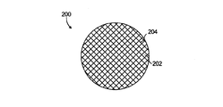
- 前記コーティングは前記透明基材中にパターンで埋め込まれている請求項1に記載のウィンドウ。
- 前記パターンには格子が含まれる請求項11に記載のウィンドウ。
- 前記コーティングと基材とは、前記パターンを通る光散乱を軽減するように屈折率が厳密に一致している請求項11に記載のウィンドウ。
- 前記伝導性コーティングは前記透明基材上の透明コーティング中にパターンで埋め込まれている請求項1に記載のウィンドウ。
- 前記コーティングと透明なベースコーティングとは、前記パターンを通る光散乱を軽減するように屈折率が厳密に一致している請求項14に記載のウィンドウ。
- 前記コーティング上の反射防止コーティングをさらに含む請求項1に記載のウィンドウ。
- 前記コーティングはシート抵抗が200オーム/スクェア未満である請求項1に記載のウィンドウ。
- ハウジングと、
前記ハウジング内に収容された撮像デバイスと、
前記ハウジングを前記撮像デバイスまで通る光路を与える前記ハウジング内のウィンドウであって、
透明基材と、
前記透明基材上のコーティングであって、前記コーティングは導電性半導体で形成され、MWIR及び/またはLWIR波長のうちの少なくとも一方に対して、前記撮像デバイスは高感度であり、前記コーティングは透明である、前記コーティングと、を含む前記ウィンドウと、
を含む光学システム。 - 前記コーティングはそのピーク透過がMWIR波長内にあり、前記撮像デバイスはMWIR波長に対して高感度である請求項18に記載のシステム。
- 前記コーティングはLWIR波長において透明であり、前記撮像デバイスはLWIR波長に対して高感度である請求項18に記載のシステム。
- 光学システム用のウィンドウを製造する方法であって、
透明基材上にコーティングを形成することであって、前記コーティングは、MWIR及び/またはLWIR波長のうちの少なくとも一方に対して透明な導電性半導体フィルムである、形成すること、を含む前記方法。
Applications Claiming Priority (2)
| Application Number | Priority Date | Filing Date | Title |
|---|---|---|---|
| US15/680,425 US10444409B2 (en) | 2017-08-18 | 2017-08-18 | MWIR/LWIR transparent, conductive coatings |
| US15/680,425 | 2017-08-18 |
Publications (2)
| Publication Number | Publication Date |
|---|---|
| JP2019036732A true JP2019036732A (ja) | 2019-03-07 |
| JP7226939B2 JP7226939B2 (ja) | 2023-02-21 |
Family
ID=63294098
Family Applications (1)
| Application Number | Title | Priority Date | Filing Date |
|---|---|---|---|
| JP2018153348A Active JP7226939B2 (ja) | 2017-08-18 | 2018-08-17 | Mwir/lwir透明伝導性コーティング |
Country Status (3)
| Country | Link |
|---|---|
| US (1) | US10444409B2 (ja) |
| EP (1) | EP3453783A3 (ja) |
| JP (1) | JP7226939B2 (ja) |
Families Citing this family (2)
| Publication number | Priority date | Publication date | Assignee | Title |
|---|---|---|---|---|
| KR20220048032A (ko) * | 2019-08-23 | 2022-04-19 | 램 리써치 코포레이션 | 플라즈마 뷰포트 |
| GB201917386D0 (en) * | 2019-11-28 | 2020-01-15 | Knapton Property Man Services Limited | Lens |
Citations (6)
| Publication number | Priority date | Publication date | Assignee | Title |
|---|---|---|---|---|
| JPH07120319A (ja) * | 1993-10-22 | 1995-05-12 | Sumitomo Electric Ind Ltd | 電波シールド性を有する赤外線透過構造体 |
| US6181468B1 (en) * | 1994-11-16 | 2001-01-30 | Raytheon Company | Composite infrared windows fabricated by direct bonding |
| JP2003177205A (ja) * | 2002-11-28 | 2003-06-27 | Mitsubishi Electric Corp | 赤外域用反射防止膜 |
| US20150289424A1 (en) * | 2014-04-07 | 2015-10-08 | Goodrich Corporation | Grid Topography For Patterned Semiconductor Coating That Minimizes Optical Scatter And Obscuration |
| WO2015199624A1 (en) * | 2014-06-23 | 2015-12-30 | Aselsan Elektronik Sanayi Ve Ticaret Anonim Şirketi | A graphene based emi shielding optical coating |
| US20160068686A1 (en) * | 2014-09-05 | 2016-03-10 | Raytheon Company | Long wave infrared transparent window and coating materials |
Family Cites Families (8)
| Publication number | Priority date | Publication date | Assignee | Title |
|---|---|---|---|---|
| US2977477A (en) | 1958-05-28 | 1961-03-28 | Rca Corp | Semiconductive materials for infrared transmissive components |
| US5012112A (en) | 1989-02-21 | 1991-04-30 | Martin Marietta Corporation | Infrared scene projector |
| DE69529505T2 (de) * | 1994-10-13 | 2003-12-11 | Raytheon Co | Leitfähige, für Infrarotstrahlung von langer Wellenlänge durchsichtige Fensterschicht |
| US6761986B2 (en) * | 2001-04-06 | 2004-07-13 | Rockwell Scientific Licensing, Llc | Thin film infrared transparent conductor |
| US7180064B2 (en) | 2003-07-24 | 2007-02-20 | Delphi Technologies, Inc. | Infrared sensor package |
| US7601946B2 (en) * | 2006-09-12 | 2009-10-13 | Ravenbrick, Llc | Electromagnetic sensor incorporating quantum confinement structures |
| US7936500B2 (en) * | 2007-03-02 | 2011-05-03 | Ravenbrick Llc | Wavelength-specific optical switch |
| US9007520B2 (en) * | 2012-08-10 | 2015-04-14 | Nanchang O-Film Optoelectronics Technology Ltd | Camera module with EMI shield |
-
2017
- 2017-08-18 US US15/680,425 patent/US10444409B2/en active Active
-
2018
- 2018-08-16 EP EP18189357.9A patent/EP3453783A3/en active Pending
- 2018-08-17 JP JP2018153348A patent/JP7226939B2/ja active Active
Patent Citations (6)
| Publication number | Priority date | Publication date | Assignee | Title |
|---|---|---|---|---|
| JPH07120319A (ja) * | 1993-10-22 | 1995-05-12 | Sumitomo Electric Ind Ltd | 電波シールド性を有する赤外線透過構造体 |
| US6181468B1 (en) * | 1994-11-16 | 2001-01-30 | Raytheon Company | Composite infrared windows fabricated by direct bonding |
| JP2003177205A (ja) * | 2002-11-28 | 2003-06-27 | Mitsubishi Electric Corp | 赤外域用反射防止膜 |
| US20150289424A1 (en) * | 2014-04-07 | 2015-10-08 | Goodrich Corporation | Grid Topography For Patterned Semiconductor Coating That Minimizes Optical Scatter And Obscuration |
| WO2015199624A1 (en) * | 2014-06-23 | 2015-12-30 | Aselsan Elektronik Sanayi Ve Ticaret Anonim Şirketi | A graphene based emi shielding optical coating |
| US20160068686A1 (en) * | 2014-09-05 | 2016-03-10 | Raytheon Company | Long wave infrared transparent window and coating materials |
Also Published As
| Publication number | Publication date |
|---|---|
| JP7226939B2 (ja) | 2023-02-21 |
| EP3453783A3 (en) | 2019-07-31 |
| US10444409B2 (en) | 2019-10-15 |
| US20190056532A1 (en) | 2019-02-21 |
| EP3453783A2 (en) | 2019-03-13 |
Similar Documents
| Publication | Publication Date | Title |
|---|---|---|
| JP3404279B2 (ja) | 高電子移動度の透明電気導体 | |
| CN110335908B (zh) | 异质结分波段探测器及其制备方法与应用 | |
| US9000551B2 (en) | High performance surface illuminating GeSi photodiodes | |
| JP2023029334A (ja) | 導電性光半導体コーティングの装置及び方法 | |
| JP7226939B2 (ja) | Mwir/lwir透明伝導性コーティング | |
| US11852977B2 (en) | Apparatus and methods of electrically conductive optical semiconductor coating | |
| JP2022183144A (ja) | 光学基板のコーティング方法、および窓 | |
| WO2015199624A1 (en) | A graphene based emi shielding optical coating | |
| US11022823B2 (en) | Switchable optical filter for imaging and optical beam modulation | |
| Hernandez-Como et al. | Low-temperature processed ZnO and CdS photodetectors deposited by pulsed laser deposition | |
| KR101720308B1 (ko) | 금속나노 입자를 이용하는 고투명 다파장 센서 및 형성 방법 | |
| EP0707347B1 (en) | Long wavelength infrared transparent conductive window | |
| US20240038906A1 (en) | Bendable Materials for Electromagnetic Interference Shielding and Detection of Infrared and Visible Radiation | |
| CN103812005A (zh) | 量子阱电致发光装置 | |
| Khanfar et al. | Polarization Sensitive Reflection and Dielectric Spectra in GaSe Thin Films. | |
| HULLAVARAD et al. | UV DETECTORS: Zinc-oxide materials and their alloys redefine UV sensing | |
| Khanfar et al. | Research Article Polarization Sensitive Reflection and Dielectric Spectra in GaSe Thin Films |
Legal Events
| Date | Code | Title | Description |
|---|---|---|---|
| A621 | Written request for application examination |
Free format text: JAPANESE INTERMEDIATE CODE: A621 Effective date: 20210219 |
|
| A977 | Report on retrieval |
Free format text: JAPANESE INTERMEDIATE CODE: A971007 Effective date: 20220225 |
|
| A131 | Notification of reasons for refusal |
Free format text: JAPANESE INTERMEDIATE CODE: A131 Effective date: 20220308 |
|
| A601 | Written request for extension of time |
Free format text: JAPANESE INTERMEDIATE CODE: A601 Effective date: 20220607 |
|
| A601 | Written request for extension of time |
Free format text: JAPANESE INTERMEDIATE CODE: A601 Effective date: 20220808 |
|
| A521 | Request for written amendment filed |
Free format text: JAPANESE INTERMEDIATE CODE: A523 Effective date: 20220908 |
|
| TRDD | Decision of grant or rejection written | ||
| A01 | Written decision to grant a patent or to grant a registration (utility model) |
Free format text: JAPANESE INTERMEDIATE CODE: A01 Effective date: 20230110 |
|
| A61 | First payment of annual fees (during grant procedure) |
Free format text: JAPANESE INTERMEDIATE CODE: A61 Effective date: 20230209 |
|
| R150 | Certificate of patent or registration of utility model |
Ref document number: 7226939 Country of ref document: JP Free format text: JAPANESE INTERMEDIATE CODE: R150 |