JP2019036732A - Mwir/lwir transparent conductive coating - Google Patents
Mwir/lwir transparent conductive coating Download PDFInfo
- Publication number
- JP2019036732A JP2019036732A JP2018153348A JP2018153348A JP2019036732A JP 2019036732 A JP2019036732 A JP 2019036732A JP 2018153348 A JP2018153348 A JP 2018153348A JP 2018153348 A JP2018153348 A JP 2018153348A JP 2019036732 A JP2019036732 A JP 2019036732A
- Authority
- JP
- Japan
- Prior art keywords
- coating
- window
- transparent
- transparent substrate
- mwir
- Prior art date
- Legal status (The legal status is an assumption and is not a legal conclusion. Google has not performed a legal analysis and makes no representation as to the accuracy of the status listed.)
- Granted
Links
- 238000000576 coating method Methods 0.000 title claims abstract description 74
- 239000011248 coating agent Substances 0.000 title claims abstract description 68
- 238000003384 imaging method Methods 0.000 claims abstract description 21
- 230000003287 optical effect Effects 0.000 claims abstract description 19
- 239000004065 semiconductor Substances 0.000 claims abstract description 19
- 239000000758 substrate Substances 0.000 claims description 38
- 230000005540 biological transmission Effects 0.000 claims description 17
- 238000005229 chemical vapour deposition Methods 0.000 claims description 9
- 229910000673 Indium arsenide Inorganic materials 0.000 claims description 7
- RPQDHPTXJYYUPQ-UHFFFAOYSA-N indium arsenide Chemical compound [In]#[As] RPQDHPTXJYYUPQ-UHFFFAOYSA-N 0.000 claims description 7
- 238000000149 argon plasma sintering Methods 0.000 claims description 6
- 239000006117 anti-reflective coating Substances 0.000 claims description 5
- 229910000530 Gallium indium arsenide Inorganic materials 0.000 claims description 4
- 229910052782 aluminium Inorganic materials 0.000 claims description 4
- XAGFODPZIPBFFR-UHFFFAOYSA-N aluminium Chemical compound [Al] XAGFODPZIPBFFR-UHFFFAOYSA-N 0.000 claims description 4
- 238000000995 aerosol-assisted chemical vapour deposition Methods 0.000 claims description 3
- 229910052751 metal Inorganic materials 0.000 claims description 3
- 239000002184 metal Substances 0.000 claims description 3
- 238000001451 molecular beam epitaxy Methods 0.000 claims description 3
- 229910052594 sapphire Inorganic materials 0.000 claims description 3
- 239000010980 sapphire Substances 0.000 claims description 3
- SBIBMFFZSBJNJF-UHFFFAOYSA-N selenium;zinc Chemical compound [Se]=[Zn] SBIBMFFZSBJNJF-UHFFFAOYSA-N 0.000 claims description 3
- 229910052596 spinel Inorganic materials 0.000 claims description 3
- 239000011029 spinel Substances 0.000 claims description 3
- 238000005118 spray pyrolysis Methods 0.000 claims description 3
- 239000000126 substance Substances 0.000 claims description 3
- 238000007740 vapor deposition Methods 0.000 claims description 3
- 238000004519 manufacturing process Methods 0.000 claims description 2
- 239000000463 material Substances 0.000 abstract description 6
- 230000035945 sensitivity Effects 0.000 abstract description 2
- 238000000034 method Methods 0.000 description 7
- 238000010521 absorption reaction Methods 0.000 description 2
- 230000003667 anti-reflective effect Effects 0.000 description 2
- 229910001111 Fine metal Inorganic materials 0.000 description 1
- GYHNNYVSQQEPJS-UHFFFAOYSA-N Gallium Chemical compound [Ga] GYHNNYVSQQEPJS-UHFFFAOYSA-N 0.000 description 1
- OAICVXFJPJFONN-UHFFFAOYSA-N Phosphorus Chemical compound [P] OAICVXFJPJFONN-UHFFFAOYSA-N 0.000 description 1
- XLOMVQKBTHCTTD-UHFFFAOYSA-N Zinc monoxide Chemical compound [Zn]=O XLOMVQKBTHCTTD-UHFFFAOYSA-N 0.000 description 1
- 229910052787 antimony Inorganic materials 0.000 description 1
- WATWJIUSRGPENY-UHFFFAOYSA-N antimony atom Chemical compound [Sb] WATWJIUSRGPENY-UHFFFAOYSA-N 0.000 description 1
- 229910052785 arsenic Inorganic materials 0.000 description 1
- RQNWIZPPADIBDY-UHFFFAOYSA-N arsenic atom Chemical compound [As] RQNWIZPPADIBDY-UHFFFAOYSA-N 0.000 description 1
- 150000001875 compounds Chemical class 0.000 description 1
- 230000007423 decrease Effects 0.000 description 1
- 239000000428 dust Substances 0.000 description 1
- 230000000694 effects Effects 0.000 description 1
- 239000007888 film coating Substances 0.000 description 1
- 238000009501 film coating Methods 0.000 description 1
- 229910052733 gallium Inorganic materials 0.000 description 1
- 229910052732 germanium Inorganic materials 0.000 description 1
- GNPVGFCGXDBREM-UHFFFAOYSA-N germanium atom Chemical compound [Ge] GNPVGFCGXDBREM-UHFFFAOYSA-N 0.000 description 1
- 229910021478 group 5 element Inorganic materials 0.000 description 1
- 229910003437 indium oxide Inorganic materials 0.000 description 1
- PJXISJQVUVHSOJ-UHFFFAOYSA-N indium(iii) oxide Chemical compound [O-2].[O-2].[O-2].[In+3].[In+3] PJXISJQVUVHSOJ-UHFFFAOYSA-N 0.000 description 1
- 238000012986 modification Methods 0.000 description 1
- 230000004048 modification Effects 0.000 description 1
- 229910052698 phosphorus Inorganic materials 0.000 description 1
- 239000011574 phosphorus Substances 0.000 description 1
- 229910052710 silicon Inorganic materials 0.000 description 1
- 239000010703 silicon Substances 0.000 description 1
Images


Classifications
-
- C—CHEMISTRY; METALLURGY
- C03—GLASS; MINERAL OR SLAG WOOL
- C03C—CHEMICAL COMPOSITION OF GLASSES, GLAZES OR VITREOUS ENAMELS; SURFACE TREATMENT OF GLASS; SURFACE TREATMENT OF FIBRES OR FILAMENTS MADE FROM GLASS, MINERALS OR SLAGS; JOINING GLASS TO GLASS OR OTHER MATERIALS
- C03C17/00—Surface treatment of glass, not in the form of fibres or filaments, by coating
-
- C—CHEMISTRY; METALLURGY
- C04—CEMENTS; CONCRETE; ARTIFICIAL STONE; CERAMICS; REFRACTORIES
- C04B—LIME, MAGNESIA; SLAG; CEMENTS; COMPOSITIONS THEREOF, e.g. MORTARS, CONCRETE OR LIKE BUILDING MATERIALS; ARTIFICIAL STONE; CERAMICS; REFRACTORIES; TREATMENT OF NATURAL STONE
- C04B35/00—Shaped ceramic products characterised by their composition; Ceramics compositions; Processing powders of inorganic compounds preparatory to the manufacturing of ceramic products
- C04B35/01—Shaped ceramic products characterised by their composition; Ceramics compositions; Processing powders of inorganic compounds preparatory to the manufacturing of ceramic products based on oxide ceramics
- C04B35/10—Shaped ceramic products characterised by their composition; Ceramics compositions; Processing powders of inorganic compounds preparatory to the manufacturing of ceramic products based on oxide ceramics based on aluminium oxide
- C04B35/111—Fine ceramics
- C04B35/115—Translucent or transparent products
-
- C—CHEMISTRY; METALLURGY
- C04—CEMENTS; CONCRETE; ARTIFICIAL STONE; CERAMICS; REFRACTORIES
- C04B—LIME, MAGNESIA; SLAG; CEMENTS; COMPOSITIONS THEREOF, e.g. MORTARS, CONCRETE OR LIKE BUILDING MATERIALS; ARTIFICIAL STONE; CERAMICS; REFRACTORIES; TREATMENT OF NATURAL STONE
- C04B41/00—After-treatment of mortars, concrete, artificial stone or ceramics; Treatment of natural stone
- C04B41/009—After-treatment of mortars, concrete, artificial stone or ceramics; Treatment of natural stone characterised by the material treated
-
- C—CHEMISTRY; METALLURGY
- C04—CEMENTS; CONCRETE; ARTIFICIAL STONE; CERAMICS; REFRACTORIES
- C04B—LIME, MAGNESIA; SLAG; CEMENTS; COMPOSITIONS THEREOF, e.g. MORTARS, CONCRETE OR LIKE BUILDING MATERIALS; ARTIFICIAL STONE; CERAMICS; REFRACTORIES; TREATMENT OF NATURAL STONE
- C04B41/00—After-treatment of mortars, concrete, artificial stone or ceramics; Treatment of natural stone
- C04B41/45—Coating or impregnating, e.g. injection in masonry, partial coating of green or fired ceramics, organic coating compositions for adhering together two concrete elements
- C04B41/50—Coating or impregnating, e.g. injection in masonry, partial coating of green or fired ceramics, organic coating compositions for adhering together two concrete elements with inorganic materials
- C04B41/5053—Coating or impregnating, e.g. injection in masonry, partial coating of green or fired ceramics, organic coating compositions for adhering together two concrete elements with inorganic materials non-oxide ceramics
-
- C—CHEMISTRY; METALLURGY
- C04—CEMENTS; CONCRETE; ARTIFICIAL STONE; CERAMICS; REFRACTORIES
- C04B—LIME, MAGNESIA; SLAG; CEMENTS; COMPOSITIONS THEREOF, e.g. MORTARS, CONCRETE OR LIKE BUILDING MATERIALS; ARTIFICIAL STONE; CERAMICS; REFRACTORIES; TREATMENT OF NATURAL STONE
- C04B41/00—After-treatment of mortars, concrete, artificial stone or ceramics; Treatment of natural stone
- C04B41/80—After-treatment of mortars, concrete, artificial stone or ceramics; Treatment of natural stone of only ceramics
- C04B41/81—Coating or impregnation
- C04B41/85—Coating or impregnation with inorganic materials
- C04B41/87—Ceramics
-
- C—CHEMISTRY; METALLURGY
- C23—COATING METALLIC MATERIAL; COATING MATERIAL WITH METALLIC MATERIAL; CHEMICAL SURFACE TREATMENT; DIFFUSION TREATMENT OF METALLIC MATERIAL; COATING BY VACUUM EVAPORATION, BY SPUTTERING, BY ION IMPLANTATION OR BY CHEMICAL VAPOUR DEPOSITION, IN GENERAL; INHIBITING CORROSION OF METALLIC MATERIAL OR INCRUSTATION IN GENERAL
- C23C—COATING METALLIC MATERIAL; COATING MATERIAL WITH METALLIC MATERIAL; SURFACE TREATMENT OF METALLIC MATERIAL BY DIFFUSION INTO THE SURFACE, BY CHEMICAL CONVERSION OR SUBSTITUTION; COATING BY VACUUM EVAPORATION, BY SPUTTERING, BY ION IMPLANTATION OR BY CHEMICAL VAPOUR DEPOSITION, IN GENERAL
- C23C16/00—Chemical coating by decomposition of gaseous compounds, without leaving reaction products of surface material in the coating, i.e. chemical vapour deposition [CVD] processes
- C23C16/22—Chemical coating by decomposition of gaseous compounds, without leaving reaction products of surface material in the coating, i.e. chemical vapour deposition [CVD] processes characterised by the deposition of inorganic material, other than metallic material
- C23C16/30—Deposition of compounds, mixtures or solid solutions, e.g. borides, carbides, nitrides
- C23C16/301—AIII BV compounds, where A is Al, Ga, In or Tl and B is N, P, As, Sb or Bi
-
- C—CHEMISTRY; METALLURGY
- C23—COATING METALLIC MATERIAL; COATING MATERIAL WITH METALLIC MATERIAL; CHEMICAL SURFACE TREATMENT; DIFFUSION TREATMENT OF METALLIC MATERIAL; COATING BY VACUUM EVAPORATION, BY SPUTTERING, BY ION IMPLANTATION OR BY CHEMICAL VAPOUR DEPOSITION, IN GENERAL; INHIBITING CORROSION OF METALLIC MATERIAL OR INCRUSTATION IN GENERAL
- C23C—COATING METALLIC MATERIAL; COATING MATERIAL WITH METALLIC MATERIAL; SURFACE TREATMENT OF METALLIC MATERIAL BY DIFFUSION INTO THE SURFACE, BY CHEMICAL CONVERSION OR SUBSTITUTION; COATING BY VACUUM EVAPORATION, BY SPUTTERING, BY ION IMPLANTATION OR BY CHEMICAL VAPOUR DEPOSITION, IN GENERAL
- C23C16/00—Chemical coating by decomposition of gaseous compounds, without leaving reaction products of surface material in the coating, i.e. chemical vapour deposition [CVD] processes
- C23C16/22—Chemical coating by decomposition of gaseous compounds, without leaving reaction products of surface material in the coating, i.e. chemical vapour deposition [CVD] processes characterised by the deposition of inorganic material, other than metallic material
- C23C16/30—Deposition of compounds, mixtures or solid solutions, e.g. borides, carbides, nitrides
- C23C16/308—Oxynitrides
-
- C—CHEMISTRY; METALLURGY
- C23—COATING METALLIC MATERIAL; COATING MATERIAL WITH METALLIC MATERIAL; CHEMICAL SURFACE TREATMENT; DIFFUSION TREATMENT OF METALLIC MATERIAL; COATING BY VACUUM EVAPORATION, BY SPUTTERING, BY ION IMPLANTATION OR BY CHEMICAL VAPOUR DEPOSITION, IN GENERAL; INHIBITING CORROSION OF METALLIC MATERIAL OR INCRUSTATION IN GENERAL
- C23C—COATING METALLIC MATERIAL; COATING MATERIAL WITH METALLIC MATERIAL; SURFACE TREATMENT OF METALLIC MATERIAL BY DIFFUSION INTO THE SURFACE, BY CHEMICAL CONVERSION OR SUBSTITUTION; COATING BY VACUUM EVAPORATION, BY SPUTTERING, BY ION IMPLANTATION OR BY CHEMICAL VAPOUR DEPOSITION, IN GENERAL
- C23C16/00—Chemical coating by decomposition of gaseous compounds, without leaving reaction products of surface material in the coating, i.e. chemical vapour deposition [CVD] processes
- C23C16/22—Chemical coating by decomposition of gaseous compounds, without leaving reaction products of surface material in the coating, i.e. chemical vapour deposition [CVD] processes characterised by the deposition of inorganic material, other than metallic material
- C23C16/30—Deposition of compounds, mixtures or solid solutions, e.g. borides, carbides, nitrides
- C23C16/40—Oxides
- C23C16/403—Oxides of aluminium, magnesium or beryllium
-
- C—CHEMISTRY; METALLURGY
- C23—COATING METALLIC MATERIAL; COATING MATERIAL WITH METALLIC MATERIAL; CHEMICAL SURFACE TREATMENT; DIFFUSION TREATMENT OF METALLIC MATERIAL; COATING BY VACUUM EVAPORATION, BY SPUTTERING, BY ION IMPLANTATION OR BY CHEMICAL VAPOUR DEPOSITION, IN GENERAL; INHIBITING CORROSION OF METALLIC MATERIAL OR INCRUSTATION IN GENERAL
- C23C—COATING METALLIC MATERIAL; COATING MATERIAL WITH METALLIC MATERIAL; SURFACE TREATMENT OF METALLIC MATERIAL BY DIFFUSION INTO THE SURFACE, BY CHEMICAL CONVERSION OR SUBSTITUTION; COATING BY VACUUM EVAPORATION, BY SPUTTERING, BY ION IMPLANTATION OR BY CHEMICAL VAPOUR DEPOSITION, IN GENERAL
- C23C18/00—Chemical coating by decomposition of either liquid compounds or solutions of the coating forming compounds, without leaving reaction products of surface material in the coating; Contact plating
- C23C18/02—Chemical coating by decomposition of either liquid compounds or solutions of the coating forming compounds, without leaving reaction products of surface material in the coating; Contact plating by thermal decomposition
- C23C18/12—Chemical coating by decomposition of either liquid compounds or solutions of the coating forming compounds, without leaving reaction products of surface material in the coating; Contact plating by thermal decomposition characterised by the deposition of inorganic material other than metallic material
- C23C18/125—Process of deposition of the inorganic material
- C23C18/1258—Spray pyrolysis
-
- C—CHEMISTRY; METALLURGY
- C30—CRYSTAL GROWTH
- C30B—SINGLE-CRYSTAL GROWTH; UNIDIRECTIONAL SOLIDIFICATION OF EUTECTIC MATERIAL OR UNIDIRECTIONAL DEMIXING OF EUTECTOID MATERIAL; REFINING BY ZONE-MELTING OF MATERIAL; PRODUCTION OF A HOMOGENEOUS POLYCRYSTALLINE MATERIAL WITH DEFINED STRUCTURE; SINGLE CRYSTALS OR HOMOGENEOUS POLYCRYSTALLINE MATERIAL WITH DEFINED STRUCTURE; AFTER-TREATMENT OF SINGLE CRYSTALS OR A HOMOGENEOUS POLYCRYSTALLINE MATERIAL WITH DEFINED STRUCTURE; APPARATUS THEREFOR
- C30B29/00—Single crystals or homogeneous polycrystalline material with defined structure characterised by the material or by their shape
- C30B29/10—Inorganic compounds or compositions
- C30B29/40—AIIIBV compounds wherein A is B, Al, Ga, In or Tl and B is N, P, As, Sb or Bi
-
- G—PHYSICS
- G01—MEASURING; TESTING
- G01J—MEASUREMENT OF INTENSITY, VELOCITY, SPECTRAL CONTENT, POLARISATION, PHASE OR PULSE CHARACTERISTICS OF INFRARED, VISIBLE OR ULTRAVIOLET LIGHT; COLORIMETRY; RADIATION PYROMETRY
- G01J5/00—Radiation pyrometry, e.g. infrared or optical thermometry
- G01J5/02—Constructional details
- G01J5/08—Optical arrangements
- G01J5/0875—Windows; Arrangements for fastening thereof
-
- G—PHYSICS
- G02—OPTICS
- G02B—OPTICAL ELEMENTS, SYSTEMS OR APPARATUS
- G02B1/00—Optical elements characterised by the material of which they are made; Optical coatings for optical elements
- G02B1/10—Optical coatings produced by application to, or surface treatment of, optical elements
- G02B1/11—Anti-reflection coatings
- G02B1/113—Anti-reflection coatings using inorganic layer materials only
-
- G—PHYSICS
- G02—OPTICS
- G02B—OPTICAL ELEMENTS, SYSTEMS OR APPARATUS
- G02B1/00—Optical elements characterised by the material of which they are made; Optical coatings for optical elements
- G02B1/10—Optical coatings produced by application to, or surface treatment of, optical elements
- G02B1/11—Anti-reflection coatings
- G02B1/118—Anti-reflection coatings having sub-optical wavelength surface structures designed to provide an enhanced transmittance, e.g. moth-eye structures
-
- G—PHYSICS
- G02—OPTICS
- G02B—OPTICAL ELEMENTS, SYSTEMS OR APPARATUS
- G02B1/00—Optical elements characterised by the material of which they are made; Optical coatings for optical elements
- G02B1/10—Optical coatings produced by application to, or surface treatment of, optical elements
- G02B1/16—Optical coatings produced by application to, or surface treatment of, optical elements having an anti-static effect, e.g. electrically conducting coatings
-
- G—PHYSICS
- G02—OPTICS
- G02B—OPTICAL ELEMENTS, SYSTEMS OR APPARATUS
- G02B13/00—Optical objectives specially designed for the purposes specified below
- G02B13/14—Optical objectives specially designed for the purposes specified below for use with infrared or ultraviolet radiation
-
- G—PHYSICS
- G02—OPTICS
- G02B—OPTICAL ELEMENTS, SYSTEMS OR APPARATUS
- G02B5/00—Optical elements other than lenses
- G02B5/20—Filters
- G02B5/207—Filters comprising semiconducting materials
-
- G—PHYSICS
- G02—OPTICS
- G02B—OPTICAL ELEMENTS, SYSTEMS OR APPARATUS
- G02B5/00—Optical elements other than lenses
- G02B5/20—Filters
- G02B5/208—Filters for use with infrared or ultraviolet radiation, e.g. for separating visible light from infrared and/or ultraviolet radiation
-
- H—ELECTRICITY
- H01—ELECTRIC ELEMENTS
- H01L—SEMICONDUCTOR DEVICES NOT COVERED BY CLASS H10
- H01L31/00—Semiconductor devices sensitive to infrared radiation, light, electromagnetic radiation of shorter wavelength or corpuscular radiation and specially adapted either for the conversion of the energy of such radiation into electrical energy or for the control of electrical energy by such radiation; Processes or apparatus specially adapted for the manufacture or treatment thereof or of parts thereof; Details thereof
- H01L31/02—Details
- H01L31/0203—Containers; Encapsulations, e.g. encapsulation of photodiodes
-
- C—CHEMISTRY; METALLURGY
- C04—CEMENTS; CONCRETE; ARTIFICIAL STONE; CERAMICS; REFRACTORIES
- C04B—LIME, MAGNESIA; SLAG; CEMENTS; COMPOSITIONS THEREOF, e.g. MORTARS, CONCRETE OR LIKE BUILDING MATERIALS; ARTIFICIAL STONE; CERAMICS; REFRACTORIES; TREATMENT OF NATURAL STONE
- C04B2111/00—Mortars, concrete or artificial stone or mixtures to prepare them, characterised by specific function, property or use
- C04B2111/80—Optical properties, e.g. transparency or reflexibility
- C04B2111/805—Transparent material
-
- G—PHYSICS
- G01—MEASURING; TESTING
- G01J—MEASUREMENT OF INTENSITY, VELOCITY, SPECTRAL CONTENT, POLARISATION, PHASE OR PULSE CHARACTERISTICS OF INFRARED, VISIBLE OR ULTRAVIOLET LIGHT; COLORIMETRY; RADIATION PYROMETRY
- G01J5/00—Radiation pyrometry, e.g. infrared or optical thermometry
- G01J5/02—Constructional details
- G01J5/06—Arrangements for eliminating effects of disturbing radiation; Arrangements for compensating changes in sensitivity
- G01J2005/065—Arrangements for eliminating effects of disturbing radiation; Arrangements for compensating changes in sensitivity by shielding
Abstract
Description
本開示は、光学コーティング、より詳細には導電性光学コーティングに関する。 The present disclosure relates to optical coatings, and more particularly to conductive optical coatings.
電気光学(EO)システムでは、センサ及びエレクトロニクスを外部環境から保護するウィンドウが必要である。雨、ホコリなどに加えて、多くの場合に、ウィンドウは、そうしなければEOシステム性能を妨げる電磁妨害(EMI)もブロックしなければならない。 Electro-optic (EO) systems require windows that protect the sensors and electronics from the outside environment. In addition to rain, dust, etc., in many cases the window must also block electromagnetic interference (EMI) that would otherwise interfere with EO system performance.
EMI遮蔽は導電性かつ光透過性のウィンドウを用いて行なうことができる。従来は3つのタイプの遮蔽がある。 EMI shielding can be performed using a conductive and light transmissive window. Conventionally, there are three types of shielding.
第1のタイプのEMI遮蔽ウィンドウは、半導体材料(たとえば、ケイ素またはゲルマニウム)にV族元素(たとえば、リン、ヒ素、またはアンチモン)をドープしたものを用いて付加的な電子を供給し、導電性を得ている。これらのウィンドウは可視波長に対しては不透明であるため、広帯域のEOシステムに対しては有用ではない。 A first type of EMI shielding window provides additional electrons using a semiconductor material (eg, silicon or germanium) doped with a group V element (eg, phosphorus, arsenic, or antimony), and is conductive. Have gained. These windows are not useful for broadband EO systems because they are opaque to visible wavelengths.
第2のタイプの遮蔽ウィンドウは、連続した透明な伝導性コーティングを用いている。これらのコーティングは、ワイドバンドギャップ半導体からなり、たとえば、酸化インジウム(In2O3)及び酸化亜鉛(ZnO)(広帯域の光透過性を有する)である。半導体にドープして導電性を得ている。しかし、ドーピングが増えて導電性及びEMI減衰が増すと、光透過度が減る。この効果は、電子からのフリーキャリア吸収及びプラズマ反射の両方によって透過率が減少するより長い波長において始まる。従来の透明な伝導性半導体コーティングは、0.4〜2.0ミクロン範囲(短波長可視から短波長赤外(SWIR)まで)においてのみ実用的である。 The second type of shielding window uses a continuous transparent conductive coating. These coatings are made of a wide band gap semiconductor, for example, indium oxide (In 2 O 3 ) and zinc oxide (ZnO) (having broadband optical transparency). Conductivity is obtained by doping a semiconductor. However, as doping increases and conductivity and EMI attenuation increase, light transmission decreases. This effect begins at longer wavelengths where the transmission is reduced by both free carrier absorption and plasma reflection from the electrons. Conventional transparent conductive semiconductor coatings are practical only in the 0.4 to 2.0 micron range (from short wavelength visible to short wavelength infrared (SWIR)).
第3のタイプの遮蔽ウィンドウは従来、可視から長波長赤外(LWIR)までの広帯域応用例に対して必要とされている。微細な金属線の格子がウィンドウの表面に付与される。典型的な寸法は5ミクロン幅ラインで140ミクロン間隔である。これらの格子状ウィンドウによって、広波長範囲に渡って光透過が可能になるが、不透明化及び散乱によって光透過が制限される。 A third type of shielding window is conventionally required for broadband applications from visible to long wavelength infrared (LWIR). A fine metal wire grid is applied to the surface of the window. Typical dimensions are 140 micron intervals with 5 micron wide lines. These lattice windows allow light transmission over a wide wavelength range, but light transmission is limited by opacification and scattering.
米国特許第9,276,034号には、伝導性格子からの光散乱を低減するための方法が示されている。経路をウィンドウ基材中にエッチングして、ウィンドウの表面が平坦になるように経路内に導電性半導体を堆積させる。半導体は、可視及び短波長赤外(SWIR)波長に対しては透明であるが、中波長赤外(MWIR)及びより長い波長に対しては反射及び吸収する。屈折率が基材のそれに近い半導体を用いて、格子線からの光散乱を最小限にする。代替的に、ドープされた導電性半導体格子を、屈折率が近くて広帯域の光透過性を伴うアンドープの半導体コーティング内に埋め込むことができる。 U.S. Pat. No. 9,276,034 shows a method for reducing light scattering from a conductive grating. The path is etched into the window substrate to deposit a conductive semiconductor in the path so that the surface of the window is flat. Semiconductors are transparent for visible and short wavelength infrared (SWIR) wavelengths, but reflect and absorb for medium wavelength infrared (MWIR) and longer wavelengths. A semiconductor with a refractive index close to that of the substrate is used to minimize light scattering from the grating lines. Alternatively, a doped conductive semiconductor grating can be embedded in an undoped semiconductor coating with a close refractive index and broadband optical transparency.
従来技術は、その使用目的に対しては満足のいくものであると考えられている。しかし導電性光学コーティングの改良が、たとえばMWIR及びLWIR光学部品に対して、常に求められている。本開示ではこの問題に対する解決方法を示す。 The prior art is considered satisfactory for its intended use. However, improvements in conductive optical coatings are always sought, for example for MWIR and LWIR optical components. The present disclosure provides a solution to this problem.
ウィンドウが、透明基材と透明基材上のコーティングとを含んでいる。コーティングは、MWIR及び/またはLWIR波長のうちの少なくとも一方に対して透明な導電性半導体で形成される。 The window includes a transparent substrate and a coating on the transparent substrate. The coating is formed of a conductive semiconductor that is transparent to at least one of the MWIR and / or LWIR wavelengths.
コーティングはそのピーク透過がMWIR波長内にあることができる。透明基材は、サファイア、酸窒化アルミニウム(AlON)、及び/またはスピネルを含むことができる。 The coating can have its peak transmission in the MWIR wavelength. The transparent substrate can include sapphire, aluminum oxynitride (AlON), and / or spinel.
コーティングはLWIR波長において透明であることができる。透明基材はZnS及び/またはZnSeのうちの少なくとも一方を含むことができる。 The coating can be transparent at the LWIR wavelength. The transparent substrate can include at least one of ZnS and / or ZnSe.
コーティングには、InAs、InGaAs、及び/またはInAlAsを含むことができる。コーティングにTe、S、Se、Si、またはSnをドープして付加的な電子を供給し、導電性を増加させることができる。コーティングを透明基材内または基材上のベースコーティング内にパターンで埋め込むことができる。パターンには格子を含むことができる。コーティングと、基材またはベースコーティングとは、パターンを通る光散乱を軽減するように屈折率が厳密に一致することができる。コーティングは、シート抵抗が200オーム/スクェア未満とすることができる。反射防止コーティングをコーティング上に含めることができる。 The coating can include InAs, InGaAs, and / or InAlAs. The coating can be doped with Te, S, Se, Si, or Sn to provide additional electrons to increase conductivity. The coating can be embedded in a pattern in the transparent substrate or in the base coating on the substrate. The pattern can include a grid. The refractive index of the coating and the substrate or base coating can be closely matched to reduce light scattering through the pattern. The coating can have a sheet resistance of less than 200 ohms / square. An antireflective coating can be included on the coating.
光学システムが、ハウジングと、ハウジング内に収容された撮像デバイスと、ハウジングを撮像デバイスまで通る光路を与えるハウジング内のウィンドウとを含む。ウィンドウには透明基材と透明基材上のコーティングとが含まれる。コーティングは導電性半導体で形成されている。MWIR及び/またはLWIR波長のうちの少なくとも一方に対して、撮像デバイスは高感度であり、コーティングは透明である。 The optical system includes a housing, an imaging device housed in the housing, and a window in the housing that provides an optical path through the housing to the imaging device. The window includes a transparent substrate and a coating on the transparent substrate. The coating is made of a conductive semiconductor. For at least one of the MWIR and / or LWIR wavelengths, the imaging device is sensitive and the coating is transparent.
光学システム用のウィンドウを製造する方法は、透明基材上にコーティングを形成することを含む。コーティングを透明基材上にフィルムとして形成することは、有機金属化学気相成長法(MOCVD)、蒸着、分子線エピタキシ(MBE)、化学スプレー熱分解、化学気相成長法(CVD)、及び/またはエアロゾルアシストCVDのうちの少なくとも1つによって可能である。 A method of manufacturing a window for an optical system includes forming a coating on a transparent substrate. Forming the coating as a film on a transparent substrate includes metal organic chemical vapor deposition (MOCVD), vapor deposition, molecular beam epitaxy (MBE), chemical spray pyrolysis, chemical vapor deposition (CVD), and / or Or by at least one of aerosol assisted CVD.
主題の開示のシステム及び方法のこれら及び他の特徴は、図面とともに取り入れた好ましい実施形態の以下の詳細な説明から当業者により容易に明らかになる。 These and other features of the subject disclosure system and method will be readily apparent to those skilled in the art from the following detailed description of the preferred embodiment taken in conjunction with the drawings.
主題の開示が属する分野の当業者であれば、主題の開示のデバイス及び方法の製造及び使用方法が、必要以上の実験作業を伴わずに容易に理解できるように、本明細書ではその好ましい実施形態をある特定の図を参照して以下に詳細に説明する。 In order that those skilled in the art to which the subject disclosure belongs will readily understand how to make and use the subject disclosure devices and methods without undue experimental work, the preferred implementations herein. The form is described in detail below with reference to certain specific figures.
次に、同様の参照符号は主題の開示の同様の構造的特徴または態様を特定する図面を参照する。説明及び例示を目的として、また限定を目的とすることなく、開示による撮像システムに対するウィンドウの典型的な実施形態の部分図を図1に示し、参照文字100によって全般的に指定する。開示またはその態様によるウィンドウの他の実施形態を図2〜4に示す。これについては説明する。本明細書で説明するシステム及び方法を用いて、ウィンドウに、撮像システム対する電磁妨害(EMI)遮蔽を与えることができる。 Like reference numerals refer now to the drawings that identify like structural features or aspects of the subject disclosure. For purposes of explanation and illustration, and without limitation, a partial view of an exemplary embodiment of a window for an imaging system according to the disclosure is shown in FIG. Other embodiments of windows according to the disclosure or aspects thereof are shown in FIGS. This will be described. Using the systems and methods described herein, the window can be provided with electromagnetic interference (EMI) shielding for the imaging system.
ウィンドウ100は、透明基材102と、透明基材102上のコーティング104とを含んでいる。コーティング104は導電性半導体で形成されている。導電性半導体は、中波長赤外(MWIR)及び/または長波長赤外(LWIR)波長のうちの少なくとも一方に対して透明である。たとえば、実施形態において、コーティング104はそのピーク透過がMWIR波長内にあり、透明基材102には、サファイア、酸窒化アルミニウム(AlON)、及び/またはスピネルが含まれる。コーティングにTe、S、Se、Si、またはSnをドープして付加的な電子を供給して、導電性を増加させることができる。このピーク透過に対する好適なコーティング104はInAs、TeドープされたInAsフィルム(InAs:Te)である。これは、3〜12ミクロン範囲において吸収が低く、ピーク透過は、反射防止(AR)コーティングがない状態で、4.6〜5.1ミクロンにおいて80%を超える。コーティング104上に任意の反射防止コーティング106を設けると、ウィンドウ100を通る透過率が増加する。この応用例に対する他の好適なコーティング材料には、InGaAs及び/またはInAlAsが含まれる。これらの材料によって、コーティング104はシート抵抗が200オーム/スクェア未満となることができ、電子易動度は撮像デバイスに対するEMI遮蔽をもたらすのに十分となる。
またコーティング104はLWIR波長において透明であることができ、たとえばそのピーク透過がLWIR波長内にあることができると考えられる。このような応用例に対する透明基材102には、ZnS及び/またはZnSeのうちの少なくとも一方を含むことができる。III族元素(たとえば、アルミニウムまたはガリウム)をInAsに加えることによって、バンドギャップが大きくなり、より短い波長に対する透過が拡大された化合物(InGaAs、InAlAs)が形成される。しかし、このような材料はInAsよりも電子移動度が小さく、長波長透過が低いと予想される。したがって、LWIR透過に対してSWIRとMWIRとの間には妥協が存在する。
It is also contemplated that coating 104 can be transparent at the LWIR wavelength, for example, its peak transmission can be within the LWIR wavelength. The
コーティング104は透明基材102上にフィルムとして形成される。これは、有機金属化学気相成長法(MOCVD)、蒸着、分子線エピタキシ(MBE)、化学スプレー熱分解、化学気相成長法(CVD)、エアロゾルアシストCVD、及び/または任意の他の好適なプロセスによって行うことができる。
The
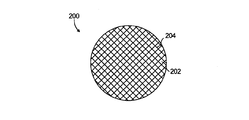
次に図2を参照して、ウィンドウ200の別の典型的な実施形態を透明基材202とともに示す。コーティング204は、透明基材202内にパターンで埋め込まれている。反射防止コーティング206を、基材202及びコーティング206のパターニングされた表面上に任意で含めることができる。図3に示すように、パターンには、格子または任意の他の好適なパターンを含めることができる。コーティング204と、基材202または基材上のベースコーティングとは、パターンを通る光散乱を軽減するように屈折率が厳密に一致することができる。パターンによって、ウィンドウ200の透明度をMWIR及びLWIR波長を超えて拡大することができる、たとえば、少なくとも多少のEMI遮蔽に対する導電性をやはり与える可視波長内にすることができる。
With reference now to FIG. 2, another exemplary embodiment of a
応用例に対してバランスされたより広い帯域となるようにEMI遮蔽と透明度との間のトレードオフを伴って、パターンを所定の応用例に対して選択することができる。たとえば、可視及びSWIR波長は格子がない場所(基材202がコーティング204の格子で覆われていない格子ラチス間)を透過することができ、格子自体はMWIR及びLWIR波長に対して透明とすることができる。さらに、格子線を、近い屈折率(5ミクロンにおいてn=3.5)を伴うベースコーティング内または基材202自体内に埋め込んだ場合、格子からの回折は非常に小さくなる。透過率とシート抵抗との間には妥協が存在する。なぜならば、格子によって覆われる表面積が連続コーティングよりも小さいからである。
A pattern can be selected for a given application, with a trade-off between EMI shielding and transparency so that a wider bandwidth is balanced for the application. For example, visible and SWIR wavelengths can be transmitted where there is no grating (between grating lattices where the
次に図4を参照して、光学システム10は、ハウジング12と、ハウジング内に収容された撮像デバイス14と、ハウジング12を撮像デバイス14まで通る光路(図4に破線で示す)を与えるハウジング12内の前述したウィンドウ100と、を含む。撮像デバイス14には光学部品16が含まれている。光学部品16は、画像を形成するために画像センサ18に光学的に結合されている。ウィンドウ100とハウジングとによって、内部の構成部品(たとえば、撮像デバイス14)に対するEMI遮蔽が得られる。MWIR及び/またはLWIR波長のうちの少なくとも一方に対して、撮像デバイス14のセンサ18は高感度であり、コーティングは透明である。センサ18がMWIR波長においてのみ高感度である(すなわち、そのピーク感度がMWIR波長内にある)場合、ウィンドウ100は、たとえば前述したような構成を用いて、MWIR波長においてのみ透明であれば良い。センサ18がLWIR波長に対してのみ高感度である場合、ウィンドウ100は、たとえば前述したような構成を用いて、LWIR波長においてのみ透明であれば良い。センサ18がMWIR及びLWIRにおける画像化を対象としている場合、ウィンドウ100を、MWIR及びLWIR波長の両方において透明度が得られるように、前述したように構成することができる。システム10を、図1に示すような連続フィルムコーティング104を伴うウィンドウ100を用いて説明し図示しているが、本開示の範囲から逸脱することなく、パターニングされたコーティング206を伴う図2〜3のウィンドウ200を用いることができる。
Referring now to FIG. 4, the
本開示の本方法及びシステムによって、前述したようにまた図面に示すように、MWIR及び/またはLWIR光透過を含む優れた特性を伴う導電性コーティングが得られる。主題の開示の装置及び方法を、好ましい実施形態を参照して図示し説明してきたが、当業者であれば容易に分かるように、主題の開示の範囲から逸脱することなく変形及び/または変更を施してもよい。 The methods and systems of the present disclosure provide conductive coatings with superior properties including MWIR and / or LWIR light transmission, as described above and as shown in the drawings. While the subject disclosure apparatus and method have been illustrated and described with reference to preferred embodiments, modifications and / or changes may be made without departing from the scope of the subject disclosure, as will be readily apparent to those skilled in the art. You may give it.
Claims (21)
前記透明基材上のコーティングであって、導電性半導体で形成され、MWIR及び/またはLWIR波長のうちの少なくとも一方に対して透明である前記コーティングと、
を含むウィンドウ。 A transparent substrate;
A coating on the transparent substrate, formed of a conductive semiconductor and transparent to at least one of MWIR and / or LWIR wavelengths;
A window containing
前記ハウジング内に収容された撮像デバイスと、
前記ハウジングを前記撮像デバイスまで通る光路を与える前記ハウジング内のウィンドウであって、
透明基材と、
前記透明基材上のコーティングであって、前記コーティングは導電性半導体で形成され、MWIR及び/またはLWIR波長のうちの少なくとも一方に対して、前記撮像デバイスは高感度であり、前記コーティングは透明である、前記コーティングと、を含む前記ウィンドウと、
を含む光学システム。 A housing;
An imaging device housed in the housing;
A window in the housing that provides an optical path through the housing to the imaging device;
A transparent substrate;
A coating on the transparent substrate, wherein the coating is formed of a conductive semiconductor, the imaging device is sensitive to at least one of MWIR and / or LWIR wavelengths, and the coating is transparent The window including the coating; and
Including optical system.
透明基材上にコーティングを形成することであって、前記コーティングは、MWIR及び/またはLWIR波長のうちの少なくとも一方に対して透明な導電性半導体フィルムである、形成すること、を含む前記方法。 A method of manufacturing a window for an optical system, comprising:
Forming a coating on a transparent substrate, the coating comprising forming a conductive semiconductor film that is transparent to at least one of MWIR and / or LWIR wavelengths.
Applications Claiming Priority (2)
| Application Number | Priority Date | Filing Date | Title |
|---|---|---|---|
| US15/680,425 US10444409B2 (en) | 2017-08-18 | 2017-08-18 | MWIR/LWIR transparent, conductive coatings |
| US15/680,425 | 2017-08-18 |
Publications (2)
| Publication Number | Publication Date |
|---|---|
| JP2019036732A true JP2019036732A (en) | 2019-03-07 |
| JP7226939B2 JP7226939B2 (en) | 2023-02-21 |
Family
ID=63294098
Family Applications (1)
| Application Number | Title | Priority Date | Filing Date |
|---|---|---|---|
| JP2018153348A Active JP7226939B2 (en) | 2017-08-18 | 2018-08-17 | MWIR/LWIR transparent conductive coatings |
Country Status (3)
| Country | Link |
|---|---|
| US (1) | US10444409B2 (en) |
| EP (1) | EP3453783A3 (en) |
| JP (1) | JP7226939B2 (en) |
Families Citing this family (2)
| Publication number | Priority date | Publication date | Assignee | Title |
|---|---|---|---|---|
| KR20220048032A (en) * | 2019-08-23 | 2022-04-19 | 램 리써치 코포레이션 | Plasma Viewport |
| GB201917386D0 (en) * | 2019-11-28 | 2020-01-15 | Knapton Property Man Services Limited | Lens |
Citations (6)
| Publication number | Priority date | Publication date | Assignee | Title |
|---|---|---|---|---|
| JPH07120319A (en) * | 1993-10-22 | 1995-05-12 | Sumitomo Electric Ind Ltd | Infrared transmission structure having radio shielding property |
| US6181468B1 (en) * | 1994-11-16 | 2001-01-30 | Raytheon Company | Composite infrared windows fabricated by direct bonding |
| JP2003177205A (en) * | 2002-11-28 | 2003-06-27 | Mitsubishi Electric Corp | Antireflection film for ir region |
| US20150289424A1 (en) * | 2014-04-07 | 2015-10-08 | Goodrich Corporation | Grid Topography For Patterned Semiconductor Coating That Minimizes Optical Scatter And Obscuration |
| WO2015199624A1 (en) * | 2014-06-23 | 2015-12-30 | Aselsan Elektronik Sanayi Ve Ticaret Anonim Şirketi | A graphene based emi shielding optical coating |
| US20160068686A1 (en) * | 2014-09-05 | 2016-03-10 | Raytheon Company | Long wave infrared transparent window and coating materials |
Family Cites Families (8)
| Publication number | Priority date | Publication date | Assignee | Title |
|---|---|---|---|---|
| US2977477A (en) | 1958-05-28 | 1961-03-28 | Rca Corp | Semiconductive materials for infrared transmissive components |
| US5012112A (en) | 1989-02-21 | 1991-04-30 | Martin Marietta Corporation | Infrared scene projector |
| EP0707347B1 (en) * | 1994-10-13 | 2003-01-29 | Raytheon Company | Long wavelength infrared transparent conductive window |
| US6761986B2 (en) * | 2001-04-06 | 2004-07-13 | Rockwell Scientific Licensing, Llc | Thin film infrared transparent conductor |
| US7180064B2 (en) | 2003-07-24 | 2007-02-20 | Delphi Technologies, Inc. | Infrared sensor package |
| US7601946B2 (en) * | 2006-09-12 | 2009-10-13 | Ravenbrick, Llc | Electromagnetic sensor incorporating quantum confinement structures |
| US7936500B2 (en) * | 2007-03-02 | 2011-05-03 | Ravenbrick Llc | Wavelength-specific optical switch |
| US9007520B2 (en) * | 2012-08-10 | 2015-04-14 | Nanchang O-Film Optoelectronics Technology Ltd | Camera module with EMI shield |
-
2017
- 2017-08-18 US US15/680,425 patent/US10444409B2/en active Active
-
2018
- 2018-08-16 EP EP18189357.9A patent/EP3453783A3/en active Pending
- 2018-08-17 JP JP2018153348A patent/JP7226939B2/en active Active
Patent Citations (6)
| Publication number | Priority date | Publication date | Assignee | Title |
|---|---|---|---|---|
| JPH07120319A (en) * | 1993-10-22 | 1995-05-12 | Sumitomo Electric Ind Ltd | Infrared transmission structure having radio shielding property |
| US6181468B1 (en) * | 1994-11-16 | 2001-01-30 | Raytheon Company | Composite infrared windows fabricated by direct bonding |
| JP2003177205A (en) * | 2002-11-28 | 2003-06-27 | Mitsubishi Electric Corp | Antireflection film for ir region |
| US20150289424A1 (en) * | 2014-04-07 | 2015-10-08 | Goodrich Corporation | Grid Topography For Patterned Semiconductor Coating That Minimizes Optical Scatter And Obscuration |
| WO2015199624A1 (en) * | 2014-06-23 | 2015-12-30 | Aselsan Elektronik Sanayi Ve Ticaret Anonim Şirketi | A graphene based emi shielding optical coating |
| US20160068686A1 (en) * | 2014-09-05 | 2016-03-10 | Raytheon Company | Long wave infrared transparent window and coating materials |
Also Published As
| Publication number | Publication date |
|---|---|
| EP3453783A2 (en) | 2019-03-13 |
| JP7226939B2 (en) | 2023-02-21 |
| US10444409B2 (en) | 2019-10-15 |
| EP3453783A3 (en) | 2019-07-31 |
| US20190056532A1 (en) | 2019-02-21 |
Similar Documents
| Publication | Publication Date | Title |
|---|---|---|
| JP3404279B2 (en) | Transparent electric conductor with high electron mobility | |
| CN110335908B (en) | Heterojunction waveband division detector and preparation method and application thereof | |
| US9000551B2 (en) | High performance surface illuminating GeSi photodiodes | |
| JP2023029334A (en) | Device and method for conductive optical semiconductor coating | |
| JP7226939B2 (en) | MWIR/LWIR transparent conductive coatings | |
| US11852977B2 (en) | Apparatus and methods of electrically conductive optical semiconductor coating | |
| JP2022183144A (en) | Method of coating optical substrate, and window | |
| WO2015199624A1 (en) | A graphene based emi shielding optical coating | |
| US11022823B2 (en) | Switchable optical filter for imaging and optical beam modulation | |
| Hernandez-Como et al. | Low-temperature processed ZnO and CdS photodetectors deposited by pulsed laser deposition | |
| KR101720308B1 (en) | Highly transparent visible-light photodetector and manufacturing method to fabricate highly transparent visible-light photodetector using nanoparticles | |
| EP0707347B1 (en) | Long wavelength infrared transparent conductive window | |
| JP2024061844A (en) | Method for coating optical substrates and windows | |
| KR102664498B1 (en) | UIM(Universal Impedance Matching) anti-reflection coating, UIM anti-reflection coating silicon photodetector that prevents reflection regardless of incident angle and polarization state in the visible and near-infrared wavelength bands and method for manufacturing the same | |
| US20240038906A1 (en) | Bendable Materials for Electromagnetic Interference Shielding and Detection of Infrared and Visible Radiation | |
| CN103812005A (en) | Quantum well electroluminescent device | |
| Khanfar et al. | Polarization Sensitive Reflection and Dielectric Spectra in GaSe Thin Films. | |
| HULLAVARAD et al. | UV DETECTORS: Zinc-oxide materials and their alloys redefine UV sensing | |
| Khanfar et al. | Research Article Polarization Sensitive Reflection and Dielectric Spectra in GaSe Thin Films |
Legal Events
| Date | Code | Title | Description |
|---|---|---|---|
| A621 | Written request for application examination |
Free format text: JAPANESE INTERMEDIATE CODE: A621 Effective date: 20210219 |
|
| A977 | Report on retrieval |
Free format text: JAPANESE INTERMEDIATE CODE: A971007 Effective date: 20220225 |
|
| A131 | Notification of reasons for refusal |
Free format text: JAPANESE INTERMEDIATE CODE: A131 Effective date: 20220308 |
|
| A601 | Written request for extension of time |
Free format text: JAPANESE INTERMEDIATE CODE: A601 Effective date: 20220607 |
|
| A601 | Written request for extension of time |
Free format text: JAPANESE INTERMEDIATE CODE: A601 Effective date: 20220808 |
|
| A521 | Request for written amendment filed |
Free format text: JAPANESE INTERMEDIATE CODE: A523 Effective date: 20220908 |
|
| TRDD | Decision of grant or rejection written | ||
| A01 | Written decision to grant a patent or to grant a registration (utility model) |
Free format text: JAPANESE INTERMEDIATE CODE: A01 Effective date: 20230110 |
|
| A61 | First payment of annual fees (during grant procedure) |
Free format text: JAPANESE INTERMEDIATE CODE: A61 Effective date: 20230209 |
|
| R150 | Certificate of patent or registration of utility model |
Ref document number: 7226939 Country of ref document: JP Free format text: JAPANESE INTERMEDIATE CODE: R150 |