JP2018536285A - Field effect transistor with optimized performance and gain - Google Patents
Field effect transistor with optimized performance and gain Download PDFInfo
- Publication number
- JP2018536285A JP2018536285A JP2018522143A JP2018522143A JP2018536285A JP 2018536285 A JP2018536285 A JP 2018536285A JP 2018522143 A JP2018522143 A JP 2018522143A JP 2018522143 A JP2018522143 A JP 2018522143A JP 2018536285 A JP2018536285 A JP 2018536285A
- Authority
- JP
- Japan
- Prior art keywords
- sublayer
- buffer layer
- field effect
- effect transistor
- interface
- Prior art date
- Legal status (The legal status is an assumption and is not a legal conclusion. Google has not performed a legal analysis and makes no representation as to the accuracy of the status listed.)
- Pending
Links
- 230000005669 field effect Effects 0.000 title claims description 16
- 239000004065 semiconductor Substances 0.000 claims abstract description 30
- 230000010287 polarization Effects 0.000 claims abstract description 19
- 230000002269 spontaneous effect Effects 0.000 claims abstract description 12
- 230000005684 electric field Effects 0.000 claims abstract description 7
- 101100495256 Caenorhabditis elegans mat-3 gene Proteins 0.000 claims abstract 4
- 230000001939 inductive effect Effects 0.000 claims abstract 2
- 229910052782 aluminium Inorganic materials 0.000 claims description 36
- XAGFODPZIPBFFR-UHFFFAOYSA-N aluminium Chemical compound [Al] XAGFODPZIPBFFR-UHFFFAOYSA-N 0.000 claims description 33
- 239000012535 impurity Substances 0.000 claims description 24
- 229910002704 AlGaN Inorganic materials 0.000 claims description 17
- 230000004888 barrier function Effects 0.000 claims description 14
- XEEYBQQBJWHFJM-UHFFFAOYSA-N Iron Chemical compound [Fe] XEEYBQQBJWHFJM-UHFFFAOYSA-N 0.000 claims description 10
- OKTJSMMVPCPJKN-UHFFFAOYSA-N Carbon Chemical compound [C] OKTJSMMVPCPJKN-UHFFFAOYSA-N 0.000 claims description 5
- FYYHWMGAXLPEAU-UHFFFAOYSA-N Magnesium Chemical compound [Mg] FYYHWMGAXLPEAU-UHFFFAOYSA-N 0.000 claims description 5
- 229910052790 beryllium Inorganic materials 0.000 claims description 5
- ATBAMAFKBVZNFJ-UHFFFAOYSA-N beryllium atom Chemical compound [Be] ATBAMAFKBVZNFJ-UHFFFAOYSA-N 0.000 claims description 5
- 229910052799 carbon Inorganic materials 0.000 claims description 5
- 229910052742 iron Inorganic materials 0.000 claims description 5
- 229910052749 magnesium Inorganic materials 0.000 claims description 4
- 239000011777 magnesium Substances 0.000 claims description 4
- 101100491335 Caenorhabditis elegans mat-2 gene Proteins 0.000 claims 3
- 102100040428 Chitobiosyldiphosphodolichol beta-mannosyltransferase Human genes 0.000 claims 1
- 101000891557 Homo sapiens Chitobiosyldiphosphodolichol beta-mannosyltransferase Proteins 0.000 claims 1
- 229910002601 GaN Inorganic materials 0.000 description 29
- 239000008186 active pharmaceutical agent Substances 0.000 description 19
- 239000007789 gas Substances 0.000 description 10
- 239000013078 crystal Substances 0.000 description 9
- 229910052757 nitrogen Inorganic materials 0.000 description 9
- 125000004429 atom Chemical group 0.000 description 8
- 150000001875 compounds Chemical class 0.000 description 8
- 229910052738 indium Inorganic materials 0.000 description 7
- IJGRMHOSHXDMSA-UHFFFAOYSA-N Atomic nitrogen Chemical compound N#N IJGRMHOSHXDMSA-UHFFFAOYSA-N 0.000 description 6
- 230000000694 effects Effects 0.000 description 6
- -1 nitride compound Chemical class 0.000 description 6
- 239000000463 material Substances 0.000 description 5
- 230000009467 reduction Effects 0.000 description 5
- 239000000758 substrate Substances 0.000 description 5
- 239000006185 dispersion Substances 0.000 description 4
- GYHNNYVSQQEPJS-UHFFFAOYSA-N Gallium Chemical group [Ga] GYHNNYVSQQEPJS-UHFFFAOYSA-N 0.000 description 3
- 230000008859 change Effects 0.000 description 3
- 125000004433 nitrogen atom Chemical group N* 0.000 description 3
- 230000005533 two-dimensional electron gas Effects 0.000 description 3
- 229910052984 zinc sulfide Inorganic materials 0.000 description 3
- JMASRVWKEDWRBT-UHFFFAOYSA-N Gallium nitride Chemical compound [Ga]#N JMASRVWKEDWRBT-UHFFFAOYSA-N 0.000 description 2
- 230000009471 action Effects 0.000 description 2
- 230000015556 catabolic process Effects 0.000 description 2
- 230000007423 decrease Effects 0.000 description 2
- 238000006731 degradation reaction Methods 0.000 description 2
- 229910052733 gallium Inorganic materials 0.000 description 2
- APFVFJFRJDLVQX-UHFFFAOYSA-N indium atom Chemical compound [In] APFVFJFRJDLVQX-UHFFFAOYSA-N 0.000 description 2
- 229910052751 metal Inorganic materials 0.000 description 2
- 239000002184 metal Substances 0.000 description 2
- 238000007725 thermal activation Methods 0.000 description 2
- 229910052720 vanadium Inorganic materials 0.000 description 2
- XUIMIQQOPSSXEZ-UHFFFAOYSA-N Silicon Chemical compound [Si] XUIMIQQOPSSXEZ-UHFFFAOYSA-N 0.000 description 1
- HCHKCACWOHOZIP-UHFFFAOYSA-N Zinc Chemical compound [Zn] HCHKCACWOHOZIP-UHFFFAOYSA-N 0.000 description 1
- AZDRQVAHHNSJOQ-UHFFFAOYSA-N alumane Chemical group [AlH3] AZDRQVAHHNSJOQ-UHFFFAOYSA-N 0.000 description 1
- 230000003321 amplification Effects 0.000 description 1
- 230000015572 biosynthetic process Effects 0.000 description 1
- 229910052796 boron Inorganic materials 0.000 description 1
- 238000004364 calculation method Methods 0.000 description 1
- 239000002131 composite material Substances 0.000 description 1
- 230000003247 decreasing effect Effects 0.000 description 1
- 230000007547 defect Effects 0.000 description 1
- 230000006872 improvement Effects 0.000 description 1
- 239000012212 insulator Substances 0.000 description 1
- 230000007246 mechanism Effects 0.000 description 1
- 238000001451 molecular beam epitaxy Methods 0.000 description 1
- 238000003199 nucleic acid amplification method Methods 0.000 description 1
- TWNQGVIAIRXVLR-UHFFFAOYSA-N oxo(oxoalumanyloxy)alumane Chemical compound O=[Al]O[Al]=O TWNQGVIAIRXVLR-UHFFFAOYSA-N 0.000 description 1
- 230000003071 parasitic effect Effects 0.000 description 1
- 230000000737 periodic effect Effects 0.000 description 1
- 238000005036 potential barrier Methods 0.000 description 1
- 229910052710 silicon Inorganic materials 0.000 description 1
- 239000010703 silicon Substances 0.000 description 1
- HBMJWWWQQXIZIP-UHFFFAOYSA-N silicon carbide Chemical compound [Si+]#[C-] HBMJWWWQQXIZIP-UHFFFAOYSA-N 0.000 description 1
- 239000007787 solid Substances 0.000 description 1
- 239000013589 supplement Substances 0.000 description 1
- 238000000927 vapour-phase epitaxy Methods 0.000 description 1
- 229910052725 zinc Inorganic materials 0.000 description 1
- 239000011701 zinc Substances 0.000 description 1
Images


Classifications
-
- H—ELECTRICITY
- H01—ELECTRIC ELEMENTS
- H01L—SEMICONDUCTOR DEVICES NOT COVERED BY CLASS H10
- H01L29/00—Semiconductor devices adapted for rectifying, amplifying, oscillating or switching, or capacitors or resistors with at least one potential-jump barrier or surface barrier, e.g. PN junction depletion layer or carrier concentration layer; Details of semiconductor bodies or of electrodes thereof ; Multistep manufacturing processes therefor
- H01L29/66—Types of semiconductor device ; Multistep manufacturing processes therefor
- H01L29/68—Types of semiconductor device ; Multistep manufacturing processes therefor controllable by only the electric current supplied, or only the electric potential applied, to an electrode which does not carry the current to be rectified, amplified or switched
- H01L29/76—Unipolar devices, e.g. field effect transistors
- H01L29/772—Field effect transistors
- H01L29/778—Field effect transistors with two-dimensional charge carrier gas channel, e.g. HEMT ; with two-dimensional charge-carrier layer formed at a heterojunction interface
- H01L29/7782—Field effect transistors with two-dimensional charge carrier gas channel, e.g. HEMT ; with two-dimensional charge-carrier layer formed at a heterojunction interface with confinement of carriers by at least two heterojunctions, e.g. DHHEMT, quantum well HEMT, DHMODFET
- H01L29/7783—Field effect transistors with two-dimensional charge carrier gas channel, e.g. HEMT ; with two-dimensional charge-carrier layer formed at a heterojunction interface with confinement of carriers by at least two heterojunctions, e.g. DHHEMT, quantum well HEMT, DHMODFET using III-V semiconductor material
-
- H—ELECTRICITY
- H01—ELECTRIC ELEMENTS
- H01L—SEMICONDUCTOR DEVICES NOT COVERED BY CLASS H10
- H01L29/00—Semiconductor devices adapted for rectifying, amplifying, oscillating or switching, or capacitors or resistors with at least one potential-jump barrier or surface barrier, e.g. PN junction depletion layer or carrier concentration layer; Details of semiconductor bodies or of electrodes thereof ; Multistep manufacturing processes therefor
- H01L29/02—Semiconductor bodies ; Multistep manufacturing processes therefor
- H01L29/12—Semiconductor bodies ; Multistep manufacturing processes therefor characterised by the materials of which they are formed
- H01L29/20—Semiconductor bodies ; Multistep manufacturing processes therefor characterised by the materials of which they are formed including, apart from doping materials or other impurities, only AIIIBV compounds
- H01L29/2003—Nitride compounds
-
- H—ELECTRICITY
- H01—ELECTRIC ELEMENTS
- H01L—SEMICONDUCTOR DEVICES NOT COVERED BY CLASS H10
- H01L29/00—Semiconductor devices adapted for rectifying, amplifying, oscillating or switching, or capacitors or resistors with at least one potential-jump barrier or surface barrier, e.g. PN junction depletion layer or carrier concentration layer; Details of semiconductor bodies or of electrodes thereof ; Multistep manufacturing processes therefor
- H01L29/02—Semiconductor bodies ; Multistep manufacturing processes therefor
- H01L29/12—Semiconductor bodies ; Multistep manufacturing processes therefor characterised by the materials of which they are formed
- H01L29/20—Semiconductor bodies ; Multistep manufacturing processes therefor characterised by the materials of which they are formed including, apart from doping materials or other impurities, only AIIIBV compounds
- H01L29/201—Semiconductor bodies ; Multistep manufacturing processes therefor characterised by the materials of which they are formed including, apart from doping materials or other impurities, only AIIIBV compounds including two or more compounds, e.g. alloys
- H01L29/205—Semiconductor bodies ; Multistep manufacturing processes therefor characterised by the materials of which they are formed including, apart from doping materials or other impurities, only AIIIBV compounds including two or more compounds, e.g. alloys in different semiconductor regions, e.g. heterojunctions
-
- H—ELECTRICITY
- H01—ELECTRIC ELEMENTS
- H01L—SEMICONDUCTOR DEVICES NOT COVERED BY CLASS H10
- H01L29/00—Semiconductor devices adapted for rectifying, amplifying, oscillating or switching, or capacitors or resistors with at least one potential-jump barrier or surface barrier, e.g. PN junction depletion layer or carrier concentration layer; Details of semiconductor bodies or of electrodes thereof ; Multistep manufacturing processes therefor
- H01L29/02—Semiconductor bodies ; Multistep manufacturing processes therefor
- H01L29/12—Semiconductor bodies ; Multistep manufacturing processes therefor characterised by the materials of which they are formed
- H01L29/20—Semiconductor bodies ; Multistep manufacturing processes therefor characterised by the materials of which they are formed including, apart from doping materials or other impurities, only AIIIBV compounds
- H01L29/207—Semiconductor bodies ; Multistep manufacturing processes therefor characterised by the materials of which they are formed including, apart from doping materials or other impurities, only AIIIBV compounds further characterised by the doping material
Abstract
発明は、特に、バッファ層(12)を2つの部分(12a;12b)に分割する特定の厚さの思慮深く載置された第1の副層(16)を備え、第3の半導体(Mat3)を備え、その結果、バッファ層の半導体及び第3の半導体(Mat3)の圧電及び自発分極係数の間の差は、バッファ層の第1の部分(12a)と第1の副層(16)との間の第1の界面(17)において、二次元ガス(9)がチャネルに限定されるように、z軸に沿って向けられる電界を生成する第1の固定表面電荷を誘導する半導体スタックを備えるトランジスタに関する。 The invention comprises in particular a thoughtfully mounted first sublayer (16) of a certain thickness dividing the buffer layer (12) into two parts (12a; 12b), and a third semiconductor (Mat3 As a result, the difference between the piezoelectric and spontaneous polarization coefficients of the buffer layer semiconductor and the third semiconductor (Mat3) is different from the first portion (12a) of the buffer layer and the first sublayer (16). A semiconductor stack inducing a first fixed surface charge that generates an electric field directed along the z-axis so that the two-dimensional gas (9) is confined to the channel at the first interface (17) between The present invention relates to a transistor comprising:
Description
本発明は、高電子移動度電界効果トランジスタ(HEMT)に関する。 The present invention relates to a high electron mobility field effect transistor (HEMT).
本発明は、特に、電力及び低雑音増幅器として、スイッチとして、又は発振器として用いられ、且つ、通常1MHz〜100GHzの間からなる周波数範囲を扱うHEMTが製作されるスタックに関する。 The present invention relates in particular to a stack in which a HEMT is fabricated which is used as a power and low noise amplifier, as a switch or as an oscillator and handles a frequency range usually comprised between 1 MHz and 100 GHz.
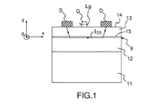
図1は、従来の基本的HEMTシステムの構造の断面をOxz平面で略図的に示しており、前記システムは基板11上に作製されている。従来、半導体又は絶縁基板11(例えば、シリコン(Si)、炭化ケイ素(SiC)、又はサファイア(Al2O3)を備える)が用いられ、その上にOxy平面に延在する少なくとも2つの半導体層のスタックEmpがz軸に沿って作製される。
FIG. 1 schematically shows a cross-section of the structure of a conventional basic HEMT system in the Oxz plane, which is fabricated on a
バッファ層と呼ばれる第1の層12は、大きなバンドギャップを有し、ワイドバンドギャップ半導体と言われ、幾つかのかかる半導体は二元化合物(GaN等)又は三元III−窒化化合物(AlGaN、又はより正確にはAlxGa1−xN等)を備え、これらは、また、III−N化合物とも称される。
The
バリア層13と呼ばれる第2の層は、バッファ層12のものよりも大きいバンドギャップを有している。この層は、Al、Ga、In、又はBをベースとした四元、三元、又は二元III−窒化(III−N)化合物ベースの半導体を備えている。
The second layer called the
例えば、GaNからできたバッファ層12と共に、バリア層13はAlxGa1−xN又はIn1−xAlxN、又はIn1−xAlxN/AlN又はAlxGa1−xN/AlN配列を備えている。アルミニウム含有量xに応じて、AlxGa1−xN及びIn1−xAlxNのバンドギャップの大きさは、それぞれ、3.4eV(GaN)から6.2eV(AlN)及び0.7eV(InN)から6.2eVに変化する。
For example, along with the
バリア層13の厚さは、通常、5nm〜40nmの間を備え、バッファ層12の厚さは、通常、0.2μm〜3μmの間を備えている。
The thickness of the
追加層が、スタックの表面上又はバッファ層12とバリア層13との間のどちらか一方に存在していてもよい。
Additional layers may be present either on the surface of the stack or between the
バッファ層12及びバリア層13は、従来、有機金属気相エピタキシー(MOVPE)又は分子線エピタキシー(MBE)によって作製されている。例として、GaNをベースとするバッファ層12とAlGaN又はInAlNをベースとする、及びより正確には、AlxGa1−xN又はInzAl1−zNをベースとするバリア層13について言及してもよく、xは通常15%〜35%の間を備え、zは通常15%〜25%の間を備える。
The
バッファ層12とバリア層13との間の接合部は、Oxy平面にも延在するヘテロ接合15を形成している。座標系Oxyzの原点Oはこの平面内に位置するよう選択される。
The junction between the
HEMTは、従来、バリア層13の上側14上に堆積されるソースS、ドレインD、及びゲートGを備えている。
The HEMT conventionally comprises a source S, a drain D, and a gate G that are deposited on the
ゲートGは、ソースSとドレインDとの間に堆積され、トランジスタが制御されることを可能にしている。 A gate G is deposited between the source S and the drain D, allowing the transistor to be controlled.
ソースSとドレインDとの間の電流は、ゲートG(ショットキー又はMISタイプの、MISは金属/絶縁体/半導体の略)の静電作用により、ヘテロ接合15の近傍に限定される二次元電子ガス9(2DEG)に関して変調される。ゲートGとソースSとの間に印加される電圧VGSはトランジスタを流れる電流を制御する。
The current between the source S and the drain D is limited to the vicinity of the
これらの電子はOxy平面において可動であり、通常1000cm2/Vsよりも大きい高電子移動度μeを有している。通常動作において、これらの電子は、それらがヘテロ接合15の近傍のOxy平面に形成するポテンシャル井戸に限定されているため、z方向に流れることができない。トランジスタのチャネルと呼ばれるものに限定される電子ガス9は、従って、電流IDSを搬送することが可能であり、この電流はドレインDとソースSとの間を流れる。従来、電位差VDSはソースSとドレインDとの間に印加され、通常ソースSが接地に接続され、電流IDSの値はゲートGとソースSとの間に印加される電圧VGSの関数である。
These electrons are movable in the Oxy plane and usually have a high electron mobility μe greater than 1000 cm 2 / Vs. In normal operation, these electrons cannot flow in the z direction because they are limited to the potential well that they form in the Oxy plane near the
トランジスタの相互コンダクタンスgmは電流IDSと電圧VGSの割合として定義される。言い換えれば、相互コンダクタンスはドレイン電流の変化を定数VDSにおけるゲートのバイアスVGSの関数として表している。 The transconductance g m of the transistor is defined as the ratio of the current I DS and the voltage V GS . In other words, the transconductance represents the change in drain current as a function of the gate bias V GS at the constant V DS .
トランジスタの利得はその相互コンダクタンスに関連する。利得は相互コンダクタンスgmに比例して増加し、ゲートGに印加される弱信号がドレインD上でより強い信号に変換されることを可能にしている。 The gain of a transistor is related to its transconductance. Gain is it possible weak signal increases in proportion to the transconductance g m, is applied to the gate G is converted to a stronger signal on the drain D.
図2は、ヘテロ接合15の近傍における電荷分布を示している。III−N族の半導体は電気的陰性が高い。この族の2つの異なる化合物が接触して載置される場合、圧電性の正σ+又は負σ−の固定電荷が、図2に示すように、界面に現れる。結果として生じる固定表面電荷は、移動電荷、すなわち、図2のように正である場合に電子を、若しくは、負である場合に正孔を引き寄せる。これは、電圧がドレインDとソースSとの間に印加される場合に電流を生成するこれらの移動電荷emである。
FIG. 2 shows the charge distribution near the
GaNは、従来の成長条件下で、ドナー型(n型)の不純物、通常、窒素空孔をドープされる半導体である。この種の欠陥は、トランジスタのドレインに印加される電圧が高くなり過ぎる場合、通常10Vよりも高くなる場合に、且つ、ゲートの長さLgが短くなり過ぎる場合、通常0.25μmよりも短くなる場合に、電子がチャネルに効果的に限定されることを可能にしない。電子は次いでバッファ層12を流れ、これが、
−相互コンダクタンスgm、及び従って、トランジスタの利得の低下(図3の範囲1)、
−伝達曲線の指数領域(図3の範囲2)における閾値下の振れ(SS=n(kbT/q)log(10))の増加。mV/decadeで表されるこの数量は、10倍毎に電流を増加させるために必要なゲート電圧の変化に対応する。室温で、及び、n=1の理想的な場合において、それは10倍当たり60mVと等しい。この数量の低下は電流を切り換える構成部品の能力を低下させる。
−漏れ電流の増加、及び従って、トランジスタの効率の低下(図3の範囲3)の原因となる。
GaN is a semiconductor doped with donor-type (n-type) impurities, usually nitrogen vacancies, under conventional growth conditions. This type of defect is usually shorter than 0.25 μm when the voltage applied to the drain of the transistor becomes too high, usually higher than 10V, and when the gate length Lg becomes too short. In some cases, it does not allow electrons to be effectively confined to the channel. The electrons then flow through the
The transconductance g m , and thus the reduction in transistor gain (
Increase in sub-threshold runout (SS = n (kbT / q) log (10)) in the exponential region of the transfer curve (
It causes an increase in leakage current and thus a reduction in the efficiency of the transistor (
無効な閉じ込めは、従って、図3で見て取れるかもしれないようなトランジスタの性能への直接的な影響を有する。 Invalid confinement thus has a direct impact on the performance of the transistor as may be seen in FIG.
図3は、電子の良好な及び不十分な閉じ込めを呈するトランジスタのためのlog(IDS)=f(VGS)のグラフ図である。 FIG. 3 is a graph of log (I DS ) = f (V GS ) for a transistor that exhibits good and insufficient confinement of electrons.
3つの範囲がその中に定義されてもよい。
−範囲1は、相互コンダクタンスgmが定義され、且つ、曲線log(IDS)=f(VGS)に関連するVGSの関数としてのIDSのグラフ図が略直線的な区分を含む。
−範囲2は、スイッチング用途に優先的に用いられる区域に対応し、特に、トランジスタの伝達特性が定義される区域に対応する。閾値下の振れSSはこの範囲において定義される。
−範囲3は、漏れ電流が定義されてもよい漸近区域に対応する。
Three ranges may be defined therein.
-
-
図3の曲線31は、チャネルに対する電子の良好な閉じ込めを呈するトランジスタのためのlog(IDS)=f(VGS)のグラフ図に対応する。高い定数VDS、例えば20Vにおいて、且つ、例えば、0.25μmよりも短いゲート長さに対して、曲線31は高い相互コンダクタンスgm、室温で60mV/decadeのその理想値に近似する閾値下の振れSS、及び、通常100μA/mmよりも小さい低い漏れ電流を有する。
図3の曲線32は、チャネルに対する電子の不十分な閉じ込めを呈するトランジスタのためのlog(IDS)=f(VGS)のグラフ図に対応する。
チャネルに対する電子の良好な閉じ込めを得るため、並びに、利得、閾値下の振れSS、及び電気効率の観点から良好なトランジスタ性能を得るために、初期のn−ドーピングを補うことが必要である。 It is necessary to supplement the initial n-doping to obtain good confinement of electrons to the channel and to obtain good transistor performance in terms of gain, sub-threshold swing SS, and electrical efficiency.
第1の解決法は、アクセプタ型の不純物を導入することによって、例えば、エピタキシャル成長条件を一部変更することによって、又は、層の成長中にアクセプタ型の不純物を添加することによって、GaN又はAlxGa1−xNを備えるバッファをp−ドープすることである。 The first solution is to introduce GaN or AlxGa1- by introducing acceptor-type impurities, for example, by partially changing the epitaxial growth conditions, or by adding acceptor-type impurities during layer growth. p-doping the buffer with xN.
バッファ層12の全体に導入される不純物密度は、所望のトランジスタ挙動を得るよう最適化される。融和性のある不純物は、主に炭素及び鉄であるが、マグネシウム、ベリリウム、又は亜鉛、若しくは、GaNにおいてアクセプタ中心であると公知の任意の不純物であってもよい。通常、1016cm−3〜1017cm−3のn型不純物に対するp型不純物の過剰は、閾値下の振れが50Vの最大動作電圧VDS及び0.15μmのゲート長さLgに対して150mV/decade未満の値に維持されることを可能にする。しかし、これらの不純物は深準位中心を形成する。
The impurity density introduced throughout the
表現「深準位中心」は、そのエネルギー準位がn型不純物のための伝導帯の最小から又はp型不純物のための価電子帯の最大から熱活性化エネルギー(3/2kbT)の2〜3倍よりも大きく位置する不純物を指すよう採用される。室温において、熱活性化エネルギーは約40meVである。 The expression “deep level center” is a 2 to 2 thermal activation energy (3/2 kb T) whose energy level is from the minimum of the conduction band for n-type impurities or from the maximum of the valence band for p-type impurities. Employed to refer to impurities located greater than three times. At room temperature, the thermal activation energy is about 40 meV.
中心は、従って、これらの極値のうちの1つから100meVよりも大きく位置する場合に深準位であると考えられ、これはアクセプタ型不純物でドープされたGaNの場合である。中心は、トランジスタがバイアスをかけられる場合、負に帯電され、それらが深準位になるにつれて、1メガヘルツよりも高い動作周波数でデチャージされる。これは、導電性チャネル内に存在する可動電荷の量を低下させる効果があり、これは電流を低下させ、アクセス抵抗を増加させる。このアプローチの主な欠点は、分散を生じることに加えて、それがトランジスタの効率及びそれが発することができる電力を低減させることであることに続く。性能におけるこの劣化は、動作電圧VDSが増加するにつれて次第に明白となり、後者は通常、20Vよりも高い。 The center is therefore considered to be a deep level when located from one of these extreme values to greater than 100 meV, which is the case for GaN doped with acceptor-type impurities. The center is negatively charged when the transistors are biased and decharged at an operating frequency higher than 1 megahertz as they go deeper. This has the effect of reducing the amount of mobile charge present in the conductive channel, which reduces the current and increases the access resistance. The main drawback of this approach follows that in addition to producing dispersion, it reduces the efficiency of the transistor and the power it can emit. This degradation in performance becomes increasingly apparent as the operating voltage VDS increases, the latter usually being higher than 20V.
電流崩壊と称される可動電荷におけるこの低下を図4に示す。この例において、GaNトランジスタのバッファ層は、5×10¹⁷atoms/cm3の値に均一にp−ドープされている。 This decrease in mobile charge, referred to as current decay, is shown in FIG. In this example, the buffer layer of the GaN transistor is uniformly p-doped to a value of 5 × 10 17 atoms / cm 3 .
曲線40は、曲線の取得前にバイアスをかけられなかったトランジスタの、VGS=0Vで取った電流/電圧曲線である。
曲線41は、曲線の取得前に電圧VGS=−6V及びVDS=40Vでのバイアスの形態を取る応力を受けた後のトランジスタの、VGS=0Vで取った電流/電圧曲線である。
曲線41において、VDSの関数としてのIDSの変化が初期曲線40に対して一部変化しており、電流/電圧特性が低下していることが見て取れるであろう。この例において、電流IDSにおける、及び従って、有能電力における60%の相対的減少が5Vの電圧VDSにおいて認められる。
It can be seen in
第2の解決法は、GaNでできたチャネルを有する、例えば、図5に示すような合成GaN/AlxGa1−xNバッファを作製することである。 The second solution is to make a synthetic GaN / Al x Ga 1-x N buffer as shown in FIG. 5, for example, with a channel made of GaN.
この場合、GaN/AlxGa1−xN界面50に現れる負の圧電性電荷は、電子がチャネルに限定されることを可能にするポテンシャル障壁を生成する。AlxGa1−xN層内の数パーセントのアルミニウム、通常3%〜10%は、20V〜40Vの間を備える最大動作電圧及び0.25μmよりも短いゲート長さに対する電子の良好な閉じ込めを得るために必要である。 In this case, the negative piezoelectric charge appearing at the GaN / Al x Ga 1-x N interface 50 creates a potential barrier that allows electrons to be confined to the channel. A few percent of aluminum in the Al x Ga 1-x N layer, typically 3% to 10%, provides good confinement of electrons for maximum operating voltages comprised between 20V and 40V and gate lengths shorter than 0.25 μm. Is necessary to get.
しかし、AlxGa1−xNの熱伝導率は、良好な電子閉じ込めのために必要なアルミニウム含有量に対して3〜5の間を備える係数で、GaNのものよりも低い。 However, the thermal conductivity of Al x Ga 1-x N is a coefficient comprising between 3 and 5 for the aluminum content necessary for good electron confinement and is lower than that of GaN.
トランジスタの熱抵抗は、従って、大幅に低下し(2〜3倍)、発せられ得る電力は、この解決法が意図される用途に応じて、1.5〜3倍低下する。 The thermal resistance of the transistor is therefore greatly reduced (2-3 times) and the power that can be emitted is reduced 1.5-3 times, depending on the application for which this solution is intended.
第1の解決法は、バッファ層12に、まさに適切な量の固定負電荷を導入して、所望の動作電圧及び周波数で良好な伝達特性を達成することにある。電子ガス9に対して電荷の量及び電荷の位置を制御することは、例えば、GaNでできているバッファの熱伝導率を低下させることなく、且つ、線形性の低下(又は、言い換えれば、分散効果)並びに有能電力及び効率の低下に通じる望ましくないトラッピング効果を生じることなく、チャネルに対する電子の良好な閉じ込めが得られることを可能にする。
The first solution is to introduce just the right amount of fixed negative charge into the
図6は、この第3の先行技術解決法による高電子移動度電界効果トランジスタ(HEMT)のためのスタック10を示している。スタック10はこの種の構成部品のために従来から用いられる種類の基板11上に作製される。
FIG. 6 shows a
スタック10はz軸と垂直なxy平面内に複数の層を備えている。
The
スタック10は、AlGaN、より正確にはAlxGa1−xN等の第1の「ワイドバンドギャップ」半導体を備えるバッファ層12を備えており、xは通常ゼロ〜35%の間を備えている。スタックのバッファ層12は、バッファ層12の特定の位置に限定される固定負電荷を備える区域Vfを備えている。
The
表現「固定負電荷」は、非可動である電荷を意味する(この文脈における可動電荷は電子又は正孔を意味する)よう理解され、用語可動は、その従来の意味において、半導体の物理学の分野内と理解される。 The expression “fixed negative charge” is understood to mean a charge that is non-movable (movable charge in this context means an electron or a hole), the term movable being in its conventional sense in the physics of semiconductors. Understood as in the field.
xy平面に延在する区域Vfはヘテロ接合から距離dに位置し、厚さtを有している。 A zone Vf extending in the xy plane is located at a distance d from the heterojunction and has a thickness t.
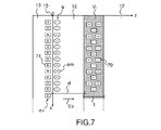
図7は、スタックにおける電荷の分布及び性質をより正確に説明している。電荷の固定特性はこの電荷を取り囲む長方形の枠によって記号で表されているのに対して、可動特性は楕円形の枠によって記号で表されている。上で説明したように、圧電効果のため、固定正電荷71の表面密度σ+はヘテロ接合15の近傍に存在し、また、ヘテロ接合15に近接して位置する負電荷emは、HEMTの動作の原点である二次元電子ガス9を形成している。チャネル内の電子表面密度emは通常、約0.5×10¹³〜3×1013cm−2である。
FIG. 7 more accurately describes the charge distribution and nature of the stack. The fixed characteristic of the charge is symbolized by a rectangular frame surrounding this charge, whereas the movable characteristic is symbolized by an elliptical frame. As described above, due to the piezoelectric effect, the surface density σ + of the fixed
良好な電子閉じ込めを得るよう(負電荷の位置及び適用量を)生じるために必要な電荷プロファイルは、動作電圧によって、ゲート長さによって、及び、トランジスタのチャネル内の電子密度によって決まる。言い換えれば、各動作電圧VDSに対して、ゲート長さ、電子密度、及び固定電荷プロファイルは最適化されなければならない。 The charge profile required to produce good electron confinement (negative charge position and dosage) depends on the operating voltage, on the gate length, and on the electron density in the transistor channel. In other words, for each operating voltage VDS, the gate length, electron density, and fixed charge profile must be optimized.
バッファ層12内に位置する固定負バルク電荷70は、バッファ層12に導入される(炭素、鉄、マグネシウムの原子又はGaN又はAlGaN内のアクセプタ中心であると公知の任意の種類の不純物等の)アクセプタ型不純物Aから得られる。
Fixed negative bulk charges 70 located in the
発明の1つの目的は、特に、高速スイッチング(エンベローブ変調)、良好な熱伝導率を有するマイクロ波信号電力増幅用途、及び使用条件に依存するバッファ層の構成を意図したトランジスタを提供することにある。 One object of the invention is to provide a transistor specifically intended for fast switching (envelope modulation), microwave signal power amplification applications with good thermal conductivity, and buffer layer configurations depending on the conditions of use. .
発明の一態様によれば、電界効果トランジスタが提供され、z軸に沿ったスタックを備える前記トランジスタは、
−第1の半導体を備えるバリア層と、
−前記バリア層とバッファ層との間のヘテロ接合と、
−z軸と垂直に位置するxy平面内及びヘテロ接合の近傍に位置するチャネルに対して制限される二次元ガスと、
−四元又は三元又は二元窒化化合物を備える第2の半導体を備えるバッファ層と、
スタックは、更に、バッファ層を2つの部分に分割する第1の副層を備え、四元又は三元又は二元窒化化合物を備える第3の半導体を備え、その結果、第2の半導体及び第3の半導体の圧電及び自発分極係数の間の差は、バッファ層の第1の部分と第1の副層との間の第1の界面において、二次元ガスがチャネルに限定されるように、z軸に沿って向けられ、第1の界面に向かう電界を生成する第1の固定表面電荷を誘導し、ヘテロ接合と、バッファ層の第1の部分と第1の副層との間に位置する第1の界面との間の距離は、トランジスタのスタックの方向Ozと垂直な方向Oxにおけるゲートの長さの3分の1とゲート長さの2倍との間を備え、z軸に沿った第1の副層の厚さは閾値よりも小さいことを特徴とする。有利に、厚さの閾値は20nmである。
According to one aspect of the invention, a field effect transistor is provided, the transistor comprising a stack along the z-axis,
A barrier layer comprising a first semiconductor;
A heterojunction between the barrier layer and the buffer layer;
A two-dimensional gas restricted to a channel located in the xy plane perpendicular to the z-axis and in the vicinity of the heterojunction;
A buffer layer comprising a second semiconductor comprising a quaternary or ternary or binary nitride compound;
The stack further comprises a first sublayer that divides the buffer layer into two parts, and comprises a third semiconductor comprising a quaternary or ternary or binary nitride compound, so that the second semiconductor and the second semiconductor The difference between the piezoelectric and spontaneous polarization coefficients of the three semiconductors is such that the two-dimensional gas is confined to the channel at the first interface between the first portion of the buffer layer and the first sublayer. Induces a first fixed surface charge directed along the z-axis and creating an electric field toward the first interface, located between the heterojunction and the first portion of the buffer layer and the first sublayer The distance between the first interface and the first interface is between the third of the gate length and twice the gate length in the direction Ox perpendicular to the stack direction Oz of the transistor, along the z-axis. Further, the thickness of the first sublayer is smaller than a threshold value. Advantageously, the thickness threshold is 20 nm.
このスタックEmpのプロファイルは、可動電荷がチャネルに対してより良好に限定されることを可能にしている。 This stack Emp profile allows the mobile charge to be better defined for the channel.
有利に、二次元ガスは電子ガスであり、バッファ層の第1の部分と第1の副層との間の界面において誘導される固定表面電荷は負であり、従って、第1の副層に向かい、且つ、チャネルに対して電子を限定する電界を生成する。 Advantageously, the two-dimensional gas is an electron gas, and the fixed surface charge induced at the interface between the first portion of the buffer layer and the first sublayer is negative, and therefore in the first sublayer. An electric field is generated that faces and limits electrons to the channel.
有利に、第2の半導体はAlxGa(1−x)Nであり、x=0%である。 Advantageously, the second semiconductor is Al x Ga (1-x) N, x = 0%.
有利に、第1の副層は、Alx1Ga(1−x1)Nを備え、x1はx+15%よりも高く、x1はこの第1の副層のアルミニウム含有量である。 Advantageously, the first sub-layer comprises a Al x1 Ga (1-x1) N, x 1 is greater than x + 15%, x 1 is the aluminum content of the first sublayer.
有利に、バッファ層は、更に、第1の副層とバッファ層の第2の部分との間に位置する第2の副層を備え、第2の副層はAlx2Ga(1−x2)Nを備え、x2はx+15%以下で、且つ、x以上であり、xはバッファ層のアルミニウム含有量であり、x2はこの第2の副層のアルミニウム含有量であり、ヘテロ接合から、第1及び第2の副層の間の第2の界面における負の固定電荷の過剰、及び、正であり、絶対値において、第1の界面の第1の固定表面電荷よりも低い第2の固定表面電荷を生じる。 Advantageously, the buffer layer further comprises a second sublayer located between the first sublayer and the second portion of the buffer layer, the second sublayer being Al x2 Ga (1-x2). N, x 2 is not more than x + 15% and not less than x, x is the aluminum content of the buffer layer, x 2 is the aluminum content of this second sublayer, and from the heterojunction, An excess of negative fixed charge at the second interface between the first and second sublayers and a second that is positive and in absolute value lower than the first fixed surface charge of the first interface Generates a fixed surface charge.
有利に、スタックの方向における第2の副層の厚さは100nm以上である。 Advantageously, the thickness of the second sublayer in the stack direction is 100 nm or more.
有利に、第2のAlGaN副層は、スタックの方向において増加し、且つ、ヘテロ接合に向かうアルミニウム濃度勾配を有し、副層19及び12b間の界面におけるアルミニウム濃度x2はx〜x+15%の間を備える。 Advantageously, the second AlGaN sublayer increases in the direction of the stack, and has an aluminum concentration gradient towards the heterojunction, the aluminum concentration x 2 at the interface between the sub-layers 19 and 12b of x~x + 15% Prepare a space.
特にAlGaNを備える第2の副層の会合は、第1の副層とバッファ層の第2の部分との間の第2の界面の近傍における電子ガスの形成が回避されることを可能にする。 The association of the second sublayer, particularly comprising AlGaN, allows the formation of electron gas in the vicinity of the second interface between the first sublayer and the second part of the buffer layer to be avoided. .
アルミニウム濃度勾配は、第2の副層の追加により生じるトランジスタの熱抵抗の低下が制限されることを可能にする。 The aluminum concentration gradient allows the reduction in transistor thermal resistance caused by the addition of the second sublayer to be limited.
有利に、第2の副層は、更に、第2の副層のアルミニウム濃度勾配によって誘導されるn型ドーピングを補うようにアクセプタ型不純物を備える。 Advantageously, the second sub-layer further comprises acceptor-type impurities to compensate for the n-type doping induced by the aluminum concentration gradient of the second sub-layer.
有利に、第2の副層に導入されるアクセプタ型不純物は、炭素又は鉄、ベリリウム又はマグネシウム又はベリリウム若しくはGaN又はAlGaNにおけるアクセプタ中心であると公知の任意の種類の不純物である。 Advantageously, the acceptor-type impurity introduced into the second sublayer is any kind of impurity known to be the acceptor center in carbon or iron, beryllium or magnesium or beryllium or GaN or AlGaN.
負に帯電される(又は、言い換えれば、負である周囲電荷の合計である)界面を生成する材料の薄層を適切に載置することにより、可動負電荷がトランジスタのチャネルに対して限定されることを可能にしている。 By properly placing a thin layer of material that creates an interface that is negatively charged (or in other words, the sum of negative ambient charges), the mobile negative charge is limited to the channel of the transistor. Making it possible.
以下の非制限的な説明を通読することで、そして、添付図面によって、発明は良好に理解され、他の利点が明らかとなるであろう。 The invention will be better understood and other advantages will become apparent upon reading the following non-limiting description and upon reference to the accompanying drawings.
発明の原理は、トランジスタの使用条件を反映しなければならない固定電荷を(不純物の形態で)添加するのではなく、スタック材料の固有特性を採用してチャネルを流れる可動電荷を限定することにある。 The principle of the invention is not to add a fixed charge (in the form of impurities) that must reflect the conditions of use of the transistor, but to employ the intrinsic properties of the stack material to limit the mobile charge flowing through the channel. .
固体において、分極の効果は、結晶の原子が、電界の作用の下で部分的又は完全に配向されてもよいか、そうでなくてもよい双極子を形成する場合に現れる。 In solids, the effect of polarization appears when the atoms of the crystal form a dipole that may or may not be partially or fully oriented under the action of an electric field.
四元、三元、又は二元半導体において、異なる電気陰性度を有する異なる性質の原子の存在のため、非対称分子が形成し、それによって永久双極子モーメントを生じる。半導体はこれらの分極効果を容易に受ける。 In quaternary, ternary or binary semiconductors, due to the presence of atoms of different properties with different electronegativity, asymmetric molecules are formed, thereby producing a permanent dipole moment. Semiconductors easily undergo these polarization effects.
分極電荷は2つのメカニズム、すなわち、自発分極及び圧電分極から生じる。 Polarization charge arises from two mechanisms: spontaneous polarization and piezoelectric polarization.
自発分極は接触する様々な原子の電気陰性度の差から生じ、圧電分極は力学的歪みから生じる。 Spontaneous polarization results from differences in electronegativity of various atoms in contact, and piezoelectric polarization results from mechanical strain.
自発分極によって、それが意味するものは、電界を受けず、且つ、分子が構成される原子の電気陰性度における差に基づいている分子の分極である。この場合、発明は、この族の材料に特有のこれら2種類の分極(自発分極及び圧電分極)の活用に基づいている(すなわち、III−N族:元素周期表の第III族の元素と窒素の会合:例えば、BN、GaN、AlN、及びInNは二元III−N化合物であり、AlGaN、InAlN、InGaN、BGaNは三元III−N化合物であり、InGaAlNは、例えば、四元III−N化合物である)。 By spontaneous polarization, what is meant is the polarization of a molecule that is not subject to an electric field and is based on the difference in electronegativity of the atoms from which the molecule is composed. In this case, the invention is based on the use of these two types of polarization (spontaneous polarization and piezoelectric polarization) characteristic of this group of materials (ie, Group III-N: Group III elements and nitrogen of the Periodic Table of Elements) For example, BN, GaN, AlN, and InN are binary III-N compounds, AlGaN, InAlN, InGaN, BGaN are ternary III-N compounds, and InGaAlN is, for example, quaternary III-N. Compound).
図8は、GaN結晶内部の電荷分布を示している。 FIG. 8 shows the charge distribution inside the GaN crystal.
ガリウム原子は窒素原子よりも電気的陰性が低い(それぞれ、1.6eV及び3eVの電気陰性度)ので、これら原子間の共有結合の電子は窒素原子により近い高い確率を有している。従って、負電荷はこれら原子の周りで合体し、正電荷はガリウム原子の周りで合体する。結晶内部の最終的な電荷分布は様々な寄与
![]()
![]()
![]()
![]()
![]()
![]()
![]()
![]()
![]()
![]()
![]()
![]()
![]()
![]()
配向されたGa−N結合([0001]結晶方向)が表面に向いている場合は、Ga面又はガリウム極性GaNと言われ、反対の場合は、N面又は窒素極性GaNと言われる。 When the oriented Ga—N bond ([0001] crystal direction) faces the surface, it is referred to as Ga face or gallium polar GaN, and in the opposite case, it is referred to as N face or nitrogen polar GaN.
N面ウルツ鉱型構造において、正電荷が表面に生じ、同じ大きさの負電荷が基板側に形成する。電荷分布は、図9が示すように、Ga面ウルツ鉱型構造の場合において反対になる。 In the N-face wurtzite structure, positive charges are generated on the surface, and negative charges of the same magnitude are formed on the substrate side. The charge distribution is reversed in the case of the Ga-plane wurtzite structure, as FIG. 9 shows.
アルミニウム原子の電気陰性度が窒素原子のものよりも低いので、自発分極から生じる電界の符号及び向きは、AlGaN層及びGaN層において全く同じである。 Since the electronegativity of aluminum atoms is lower than that of nitrogen atoms, the sign and direction of the electric field resulting from spontaneous polarization is exactly the same in the AlGaN layer and the GaN layer.
図10は、発明の一態様によるスタックを備えるトランジスタを示している。 FIG. 10 illustrates a transistor with a stack according to one aspect of the invention.
スタック10は基板11を備え、それはまた、AlN等の二元窒化化合物、若しくは、AlGaN又はInAlN、及びより正確には、AlxGa1−xN又はInyAl1−yN等の三元窒化化合物であり、xは通常15〜35%の間を備え、若しくは、BAlGaN又はInGaAlN等の四元窒化化合物を備える第1の半導体を備えるバリア層13も備えている。
The
スタック10は、バッファ層12とバリア層13との間のヘテロ接合15、及び、HEMTスタックの従来構造により、z軸と垂直なxy平面内且つヘテロ接合15の近傍に位置する二次元電子ガス9を含んでいる。
The
バッファ層12は、更に、バッファ層12を2つの部分12a及び12bに分離させる第1の副層16を備えている。第1の副層16は、ゲートの長さLgの3分の1とゲートの長さLgの2倍との間を備える距離で位置する。言い換えれば、バッファ層12の第1の部分12aの厚さはトランジスタのゲートの長さLgの3分の1とゲートの長さLgの2倍との間を備えている。
The
この場合、バッファ層12はGa面窒化ガリウムGaNを備え、第1の副層16はAlxGa1−xNを備え、アルミニウム含有量x1はx+15%よりも高く、スタック10の方向における第1の副層16の厚さtは20nmよりも小さい。他の材料を想定してもよい。しかし、頻繁に挙げられる窒化インジウムガリウムInGaNは良い候補ではない。具体的には、満足な結晶品質で数パーセントを超えるインジウムを備えるInGaNを成長させることは困難である。加えて、InGaNは、GaNを成長させるために要求されるものよりも低い200℃である温度で成長する。従って、結果として、InGaNの層上で、InGaN層の品質を低下させることなく、GaN等の化合物を良好な結晶品質で成長させることは困難である。
In this case, the
この特許において提案する解決法において、様々な材料の成長温度同士は、スタックの様々な層が満足な結晶品質で作製されることを可能にするために、かなり近似している。 In the solution proposed in this patent, the growth temperatures of the various materials are fairly close to allow the various layers of the stack to be made with satisfactory crystal quality.
層12a及び16の分極間の差のため、第1の固定負表面電荷は、バッファ層の第1の部分12aと第1の副層16との間に位置する界面17において現れる。言い換えれば、負電荷は界面17において現れ、第1の副層16のバルク内又はバッファ層の第1の部分12a内には現れない。
Due to the difference between the polarizations of the
この解決法は、特に、トランジスタの熱劣化が2℃/mm/Wよりも低い値に制限されることを可能にし、(負電荷をバッファ層12に導入するよう、従来技術による、深準位中心の使用に起因するものである)相互コンダクタンス周波数分散を生じない。 This solution makes it possible in particular to limit the thermal degradation of the transistor to a value lower than 2 ° C./mm/W, and the deep level according to the prior art (introducing negative charges into the buffer layer 12). Does not cause transconductance frequency dispersion (due to the use of the center).
二次元電子ガス9は、従って、チャネルに限定され、可動電荷はバッファ層の第1の部分12aに分散しない。
The two-
チャネルによって、意味するものは、ヘテロ接合15の近傍でバッファ層12の表面上に位置する約10nmよりも小さい厚さの層である。
By channel, what is meant is a layer of thickness less than about 10 nm located on the surface of the
第1の副層16のAlxGa1−xNの小さい厚さはトランジスタの熱抵抗の増加を2℃/mm/Wよりも低い値に制限する。
The small thickness of Al x Ga 1-x N in the first
その上、別の電子ガスが第1の副層16とバッファ層の第2の部分12bとの間の第2の界面18に形成することを防ぐために、発明の別の態様により、第1の副層16と、第1の副層16に隣接する第2の副層19、又は、言い換えれば、第2の界面18を形成するために第1の副層16と当接する第2の副層19を会合させることが提案される。第1の副層16と第2の副層19との間の第2の界面18の近傍に位置する電荷の合計は正である。
Moreover, in order to prevent another electron gas from forming at the
図11は、発明のこの態様を示している。 FIG. 11 illustrates this aspect of the invention.
スタック10は、図10におけるように、第1の副層16によって2つの部分12a及び12bに分離されるバッファ層12を備えている。この場合、スタック10は、更に、Alx2Ga1−x2Nを備える第2の副層19を備え、アルミニウム含有量x2はx+15%よりも低い。従って、第2の界面18の近傍の自発性及び圧電性電荷の(正の値)の合計が第1の界面17の自発性及び圧電性電荷の(負の値)の合計よりも低いという事実は、チャネルに対する電子の良好な閉じ込めが、マイクロ波波長領域におけるトランジスタの性能を低下させる、寄生電子ガスが界面18において形成されることを防ぐ間に得られることを可能にする。
As shown in FIG. 10, the
AlGaNの熱伝導率がアルミニウム濃度により大幅に低下する(10%のアルミニウム含有量に対して4で除算される)ので、熱抵抗を向上させるよう、第1の副層16に向けられる増大するアルミニウム濃度勾配を生成することが提案される。一定のアルミニウム濃度に対して、線形アルミニウム濃度勾配は、第2の副層に起因する熱抵抗が3〜4倍減少することを可能にする。
Since the thermal conductivity of AlGaN is greatly reduced by the aluminum concentration (divided by 4 for an aluminum content of 10%), increasing aluminum directed to the
図12は、スタックのアルミニウム濃度プロファイルP1、P2、及びP3を示している。小さい厚さ、通常20nmよりも小さい厚さの第1の副層16は、ヘテロ接合15の近傍におけるチャネルに対する電子の閉じ込めを向上させるように、高いアルミニウム含有量を備えている。第1の副層16からバッファ層の第2の部分12bへ、プロファイルP1におけるアルミニウム含有量は減少する線形勾配を有しており、アルミニウム含有量はx+0〜x+15%の間を備えている。プロファイルP2及びP3は、第2の副層19より上のアルミニウム含有量における他の減少変動を呈している。
FIG. 12 shows the aluminum concentration profiles P1, P2, and P3 of the stack. The
この濃度勾配によって誘導されるAlGaN層19のn型ドーピングを補うため、発明に対する1つの改善において、アクセプタ型不純物をAlGaN層19に導入することが提案される。
In order to compensate for the n-type doping of the
有利に、第2の副層19に導入される不純物は、鉄又は炭素又はマグネシウム又はベリリウム又はGaN又はAlGaNにおけるアクセプタ中心であると公知の任意の他の原子である。導入された不純物濃度は、この濃度勾配によって誘導されるドーピング以上である。この濃度勾配は、濃度勾配によって誘導され、AlGaN層19の厚さによって分割される圧電性及び自発性電荷の合計以上でなければならない。
Advantageously, the impurity introduced into the
図13は、電圧VDS=40Vに対する150nmのゲート長さLgの、発明によるトランジスタのためのシミュレートされたlog(IDS)=f(VGS)伝達曲線61、62、63、及び64を示している。第1の副層16は、ヘテロ接合15から100nmに位置し、5nmの厚さt1を有している。
FIG. 13 shows simulated log (I DS ) = f (V GS ) transfer curves 61, 62, 63 and 64 for a transistor according to the invention with a gate length Lg of 150 nm for a voltage V DS = 40V. Show. The
この場合、曲線61、62、63及び64はそれぞれ、第1の副層16がそれぞれ異なるアルミニウム含有量:25、30、35、及び40%を有するトランジスタに対応している。
In this case, the
それぞれの曲線の閾値下の振れSSが10倍当たり約70mVであり、その理想値(室温で60mV/decade)に近似していることが見て取れる。この70mV/decadeの値は、アルミニウム含有量が40%である場合に電流の50倍を超えて維持され、これは1μA/mm未満の漏れ電流が達成されることを可能にし、電力消費が重要な基準である用途にとって真価を示す。 It can be seen that the sub-threshold runout SS of each curve is about 70 mV per 10 times and approximates its ideal value (60 mV / decade at room temperature). This 70 mV / decade value is maintained over 50 times the current when the aluminum content is 40%, which allows a leakage current of less than 1 μA / mm to be achieved and power consumption is important It shows true value for the use that is a standard.
Claims (9)
−第1の半導体(Mat1)を備えるバリア層(13)と、
−前記バリア層(13)とバッファ層(12)との間のヘテロ接合(15)と、
−前記z軸と垂直に位置するxy平面内及び前記ヘテロ接合(15)の近傍に位置するチャネルに対して制限される二次元ガス(9)と、
−AlxGa(1−x)Nを備える第2の半導体(Mat2)を備える前記バッファ層(12)であって、xは前記バッファ層(12)のアルミニウム含有量である、前記バッファ層(12)と、を備え、
前記スタックは、更に、前記バッファ層(12)を2つの部分(12a;12b)に分割する第1の副層(16)を備え、Alx1Ga(1−x1)Nを備える第3の半導体(Mat3)を備え、x1はx+15%よりも高く、x1は前記副層(16)の前記アルミニウム含有量であり、その結果、前記第2の半導体(Mat2)及び前記第3の半導体(Mat3)の圧電及び自発分極係数の間の差は、前記バッファ層の前記第1の部分(12a)と前記第1の副層(16)との間の第1の界面(17)において、前記二次元ガス(9)が前記チャネルに限定されるように、前記z軸に沿って向けられ、前記第1の界面(17)に向かう電界を生成する第1の固定表面電荷(Q1)を誘導し、前記ヘテロ接合(15)と、前記バッファ層の前記第1の部分(12a)と前記第1の副層(16)との間に位置する前記第1の界面(17)との間の距離は、前記トランジスタの前記スタックの方向Ozと垂直な方向Oxにおける前記ゲートの長さ(Lg)の3分の1と前記ゲート長さ(Lg)の2倍との間を備えることを特徴とする、
電界効果トランジスタ。 a field effect transistor comprising a stack (Emp) along the z-axis,
A barrier layer (13) comprising a first semiconductor (Mat1);
A heterojunction (15) between the barrier layer (13) and the buffer layer (12);
A two-dimensional gas (9) restricted to a channel located in the xy plane perpendicular to the z-axis and in the vicinity of the heterojunction (15);
A -Al x Ga (1-x) a second semiconductor (Mat2) said buffer comprises a layer comprising a N (12), x is the aluminum content of the buffer layer (12), said buffer layer ( 12)
The stack further comprises a first sublayer (16) that divides the buffer layer (12) into two parts (12a; 12b), and a third semiconductor comprising Al x1 Ga (1-x1) N (Mat3), x1 is higher than x + 15%, and x1 is the aluminum content of the sublayer (16), so that the second semiconductor (Mat2) and the third semiconductor (Mat3) The difference between the piezoelectric and spontaneous polarization coefficients of the first layer (12a) of the buffer layer and the first interface (17) between the first sublayer (16) Inducing a first fixed surface charge (Q1) that is directed along the z-axis such that a gas (9) is confined to the channel and generates an electric field towards the first interface (17); The heterojunction (15) and the buffer layer; The distance between the first portion (12a) and the first interface (17) located between the first sublayer (16) is perpendicular to the stack direction Oz of the transistor. Characterized in that it comprises between one third of the gate length (Lg) in the direction Ox and twice the gate length (Lg).
Field effect transistor.
Applications Claiming Priority (3)
| Application Number | Priority Date | Filing Date | Title |
|---|---|---|---|
| FR15/02296 | 2015-10-30 | ||
| FR1502296A FR3043251B1 (en) | 2015-10-30 | 2015-10-30 | FIELD EFFECT TRANSISTOR WITH OPTIMIZED EFFICIENCY AND GAIN |
| PCT/EP2016/075971 WO2017072249A1 (en) | 2015-10-30 | 2016-10-27 | Field-effect transistor with optimised performance and gain |
Publications (1)
| Publication Number | Publication Date |
|---|---|
| JP2018536285A true JP2018536285A (en) | 2018-12-06 |
Family
ID=56137366
Family Applications (1)
| Application Number | Title | Priority Date | Filing Date |
|---|---|---|---|
| JP2018522143A Pending JP2018536285A (en) | 2015-10-30 | 2016-10-27 | Field effect transistor with optimized performance and gain |
Country Status (6)
| Country | Link |
|---|---|
| US (1) | US20180308966A1 (en) |
| EP (1) | EP3369115A1 (en) |
| JP (1) | JP2018536285A (en) |
| CN (1) | CN108475696A (en) |
| FR (1) | FR3043251B1 (en) |
| WO (1) | WO2017072249A1 (en) |
Families Citing this family (5)
| Publication number | Priority date | Publication date | Assignee | Title |
|---|---|---|---|---|
| CN109742072B (en) * | 2019-01-04 | 2019-08-16 | 苏州汉骅半导体有限公司 | Integrated enhanced and depletion type HEMT and its manufacturing method |
| US11101378B2 (en) | 2019-04-09 | 2021-08-24 | Raytheon Company | Semiconductor structure having both enhancement mode group III-N high electron mobility transistors and depletion mode group III-N high electron mobility transistors |
| FR3098810B1 (en) * | 2019-07-18 | 2021-10-15 | Commissariat Energie Atomique | Mechanical connection for MEMS and NEMS device for measuring a pressure variation and device comprising such a mechanical connection |
| US11545566B2 (en) * | 2019-12-26 | 2023-01-03 | Raytheon Company | Gallium nitride high electron mobility transistors (HEMTs) having reduced current collapse and power added efficiency enhancement |
| US11362190B2 (en) | 2020-05-22 | 2022-06-14 | Raytheon Company | Depletion mode high electron mobility field effect transistor (HEMT) semiconductor device having beryllium doped Schottky contact layers |
Citations (3)
| Publication number | Priority date | Publication date | Assignee | Title |
|---|---|---|---|---|
| JP2005086102A (en) * | 2003-09-10 | 2005-03-31 | Univ Nagoya | Field effect transistor and method of manufacturing field effect transistor |
| US20100289067A1 (en) * | 2009-05-14 | 2010-11-18 | Transphorm Inc. | High Voltage III-Nitride Semiconductor Devices |
| JP2015135946A (en) * | 2014-01-16 | 2015-07-27 | エルジー エレクトロニクス インコーポレイティド | Nitride semiconductor device and method of fabricating the same |
Family Cites Families (11)
| Publication number | Priority date | Publication date | Assignee | Title |
|---|---|---|---|---|
| US6624452B2 (en) * | 2000-07-28 | 2003-09-23 | The Regents Of The University Of California | Gallium nitride-based HFET and a method for fabricating a gallium nitride-based HFET |
| JP5334149B2 (en) * | 2006-06-02 | 2013-11-06 | 独立行政法人産業技術総合研究所 | Nitride semiconductor field effect transistor |
| JP5130846B2 (en) * | 2006-10-30 | 2013-01-30 | 株式会社デンソー | Thermally conductive insulating material and manufacturing method thereof |
| JP5487631B2 (en) * | 2009-02-04 | 2014-05-07 | 富士通株式会社 | Compound semiconductor device and manufacturing method thereof |
| JP2010238752A (en) * | 2009-03-30 | 2010-10-21 | Mitsubishi Electric Corp | Semiconductor device and method of manufacturing the same |
| KR101620987B1 (en) * | 2009-04-08 | 2016-05-13 | 이피션트 파워 컨버젼 코퍼레이션 | Dopant diffusion modulation in gan buffer layers |
| JP5624940B2 (en) * | 2011-05-17 | 2014-11-12 | 古河電気工業株式会社 | Semiconductor device and manufacturing method thereof |
| CN102646700B (en) * | 2012-05-07 | 2015-01-28 | 中国电子科技集团公司第五十五研究所 | Epitaxial structure for nitride high electron mobility transistors of composite buffer layers |
| CN102969341A (en) * | 2012-11-09 | 2013-03-13 | 中国电子科技集团公司第五十五研究所 | Nitride high electronic mobility transistor extension structure of component gradually-changed ALyGal-yN buffer layer |
| US9553183B2 (en) * | 2013-06-19 | 2017-01-24 | Infineon Technologies Austria Ag | Gate stack for normally-off compound semiconductor transistor |
| US9960262B2 (en) * | 2016-02-25 | 2018-05-01 | Raytheon Company | Group III—nitride double-heterojunction field effect transistor |
-
2015
- 2015-10-30 FR FR1502296A patent/FR3043251B1/en active Active
-
2016
- 2016-10-27 CN CN201680077236.2A patent/CN108475696A/en active Pending
- 2016-10-27 EP EP16790546.2A patent/EP3369115A1/en not_active Withdrawn
- 2016-10-27 US US15/769,708 patent/US20180308966A1/en not_active Abandoned
- 2016-10-27 WO PCT/EP2016/075971 patent/WO2017072249A1/en active Application Filing
- 2016-10-27 JP JP2018522143A patent/JP2018536285A/en active Pending
Patent Citations (3)
| Publication number | Priority date | Publication date | Assignee | Title |
|---|---|---|---|---|
| JP2005086102A (en) * | 2003-09-10 | 2005-03-31 | Univ Nagoya | Field effect transistor and method of manufacturing field effect transistor |
| US20100289067A1 (en) * | 2009-05-14 | 2010-11-18 | Transphorm Inc. | High Voltage III-Nitride Semiconductor Devices |
| JP2015135946A (en) * | 2014-01-16 | 2015-07-27 | エルジー エレクトロニクス インコーポレイティド | Nitride semiconductor device and method of fabricating the same |
Also Published As
| Publication number | Publication date |
|---|---|
| CN108475696A (en) | 2018-08-31 |
| WO2017072249A1 (en) | 2017-05-04 |
| FR3043251B1 (en) | 2022-11-11 |
| FR3043251A1 (en) | 2017-05-05 |
| US20180308966A1 (en) | 2018-10-25 |
| EP3369115A1 (en) | 2018-09-05 |
Similar Documents
| Publication | Publication Date | Title |
|---|---|---|
| US10043896B2 (en) | III-Nitride transistor including a III-N depleting layer | |
| JP5160791B2 (en) | Nitride heterojunction transistor having charge transfer induced energy barrier and method of manufacturing the same | |
| US8872233B2 (en) | Semiconductor structure | |
| US8669591B2 (en) | E-mode HFET device | |
| KR101497725B1 (en) | Cascode circuit employing a depletion-mode, gan-based fet | |
| US11289593B2 (en) | Breakdown resistant HEMT substrate and device | |
| CN107731902B (en) | Layer structure of group III nitride normally-off transistor | |
| JP6732131B2 (en) | Semiconductor device and method of designing semiconductor device | |
| US20050133816A1 (en) | III-nitride quantum-well field effect transistors | |
| JP4462330B2 (en) | Group III nitride electronic devices | |
| US9231064B1 (en) | Double heterojunction group III-nitride structures | |
| JP2018536285A (en) | Field effect transistor with optimized performance and gain | |
| US9076850B2 (en) | High electron mobility transistor | |
| US20220093779A1 (en) | Gallium nitride enhancement mode device | |
| Yang et al. | High channel conductivity, breakdown field strength, and low current collapse in AlGaN/GaN/Si $\delta $-Doped AlGaN/GaN: C HEMTs | |
| US20180138304A1 (en) | High Electron Mobility Transistor with Graded Back-Barrier Region | |
| JP2009026975A (en) | Semiconductor apparatus | |
| US8659056B2 (en) | Heterojunction field-effect transistor with source electrode and insulator formed in semiconductor layer opening | |
| WO2012029292A1 (en) | Semiconductor substrate, insulated gate field effect transistor, and method for manufacturing semiconductor substrate | |
| JP2009302370A (en) | Semiconductor device | |
| US20210359123A1 (en) | Semiconductor power device | |
| US9935192B2 (en) | Optimized buffer layer for high mobility field-effect transistor | |
| JP2012069662A (en) | Field effect transistor | |
| US20140183545A1 (en) | Polarization effect carrier generating device structures having compensation doping to reduce leakage current | |
| US20180019334A1 (en) | Multilayer passivation of the upper face of the stack of semiconductor materials of a field-effect transistor |
Legal Events
| Date | Code | Title | Description |
|---|---|---|---|
| A621 | Written request for application examination |
Free format text: JAPANESE INTERMEDIATE CODE: A621 Effective date: 20191009 |
|
| A977 | Report on retrieval |
Free format text: JAPANESE INTERMEDIATE CODE: A971007 Effective date: 20200529 |
|
| A131 | Notification of reasons for refusal |
Free format text: JAPANESE INTERMEDIATE CODE: A131 Effective date: 20200616 |
|
| A601 | Written request for extension of time |
Free format text: JAPANESE INTERMEDIATE CODE: A601 Effective date: 20200910 |
|
| A521 | Request for written amendment filed |
Free format text: JAPANESE INTERMEDIATE CODE: A523 Effective date: 20201214 |
|
| A131 | Notification of reasons for refusal |
Free format text: JAPANESE INTERMEDIATE CODE: A131 Effective date: 20210202 |
|
| A601 | Written request for extension of time |
Free format text: JAPANESE INTERMEDIATE CODE: A601 Effective date: 20210426 |
|
| A521 | Request for written amendment filed |
Free format text: JAPANESE INTERMEDIATE CODE: A523 Effective date: 20210730 |
|
| A02 | Decision of refusal |
Free format text: JAPANESE INTERMEDIATE CODE: A02 Effective date: 20211116 |