JP2018511482A - Hybrid alloy solder paste - Google Patents
Hybrid alloy solder paste Download PDFInfo
- Publication number
- JP2018511482A JP2018511482A JP2017547978A JP2017547978A JP2018511482A JP 2018511482 A JP2018511482 A JP 2018511482A JP 2017547978 A JP2017547978 A JP 2017547978A JP 2017547978 A JP2017547978 A JP 2017547978A JP 2018511482 A JP2018511482 A JP 2018511482A
- Authority
- JP
- Japan
- Prior art keywords
- alloy
- solder
- solder paste
- weight
- paste
- Prior art date
- Legal status (The legal status is an assumption and is not a legal conclusion. Google has not performed a legal analysis and makes no representation as to the accuracy of the status listed.)
- Pending
Links
Images


Classifications
-
- B—PERFORMING OPERATIONS; TRANSPORTING
- B23—MACHINE TOOLS; METAL-WORKING NOT OTHERWISE PROVIDED FOR
- B23K—SOLDERING OR UNSOLDERING; WELDING; CLADDING OR PLATING BY SOLDERING OR WELDING; CUTTING BY APPLYING HEAT LOCALLY, e.g. FLAME CUTTING; WORKING BY LASER BEAM
- B23K35/00—Rods, electrodes, materials, or media, for use in soldering, welding, or cutting
- B23K35/02—Rods, electrodes, materials, or media, for use in soldering, welding, or cutting characterised by mechanical features, e.g. shape
- B23K35/0222—Rods, electrodes, materials, or media, for use in soldering, welding, or cutting characterised by mechanical features, e.g. shape for use in soldering, brazing
- B23K35/0244—Powders, particles or spheres; Preforms made therefrom
- B23K35/025—Pastes, creams, slurries
-
- B—PERFORMING OPERATIONS; TRANSPORTING
- B23—MACHINE TOOLS; METAL-WORKING NOT OTHERWISE PROVIDED FOR
- B23K—SOLDERING OR UNSOLDERING; WELDING; CLADDING OR PLATING BY SOLDERING OR WELDING; CUTTING BY APPLYING HEAT LOCALLY, e.g. FLAME CUTTING; WORKING BY LASER BEAM
- B23K35/00—Rods, electrodes, materials, or media, for use in soldering, welding, or cutting
- B23K35/22—Rods, electrodes, materials, or media, for use in soldering, welding, or cutting characterised by the composition or nature of the material
- B23K35/24—Selection of soldering or welding materials proper
- B23K35/26—Selection of soldering or welding materials proper with the principal constituent melting at less than 400 degrees C
- B23K35/262—Sn as the principal constituent
-
- B—PERFORMING OPERATIONS; TRANSPORTING
- B23—MACHINE TOOLS; METAL-WORKING NOT OTHERWISE PROVIDED FOR
- B23K—SOLDERING OR UNSOLDERING; WELDING; CLADDING OR PLATING BY SOLDERING OR WELDING; CUTTING BY APPLYING HEAT LOCALLY, e.g. FLAME CUTTING; WORKING BY LASER BEAM
- B23K35/00—Rods, electrodes, materials, or media, for use in soldering, welding, or cutting
- B23K35/22—Rods, electrodes, materials, or media, for use in soldering, welding, or cutting characterised by the composition or nature of the material
- B23K35/24—Selection of soldering or welding materials proper
- B23K35/26—Selection of soldering or welding materials proper with the principal constituent melting at less than 400 degrees C
- B23K35/264—Bi as the principal constituent
-
- C—CHEMISTRY; METALLURGY
- C22—METALLURGY; FERROUS OR NON-FERROUS ALLOYS; TREATMENT OF ALLOYS OR NON-FERROUS METALS
- C22C—ALLOYS
- C22C12/00—Alloys based on antimony or bismuth
-
- C—CHEMISTRY; METALLURGY
- C22—METALLURGY; FERROUS OR NON-FERROUS ALLOYS; TREATMENT OF ALLOYS OR NON-FERROUS METALS
- C22C—ALLOYS
- C22C13/00—Alloys based on tin
-
- C—CHEMISTRY; METALLURGY
- C22—METALLURGY; FERROUS OR NON-FERROUS ALLOYS; TREATMENT OF ALLOYS OR NON-FERROUS METALS
- C22C—ALLOYS
- C22C13/00—Alloys based on tin
- C22C13/02—Alloys based on tin with antimony or bismuth as the next major constituent
-
- C—CHEMISTRY; METALLURGY
- C22—METALLURGY; FERROUS OR NON-FERROUS ALLOYS; TREATMENT OF ALLOYS OR NON-FERROUS METALS
- C22C—ALLOYS
- C22C30/00—Alloys containing less than 50% by weight of each constituent
- C22C30/02—Alloys containing less than 50% by weight of each constituent containing copper
-
- C—CHEMISTRY; METALLURGY
- C22—METALLURGY; FERROUS OR NON-FERROUS ALLOYS; TREATMENT OF ALLOYS OR NON-FERROUS METALS
- C22C—ALLOYS
- C22C30/00—Alloys containing less than 50% by weight of each constituent
- C22C30/04—Alloys containing less than 50% by weight of each constituent containing tin or lead
-
- C—CHEMISTRY; METALLURGY
- C22—METALLURGY; FERROUS OR NON-FERROUS ALLOYS; TREATMENT OF ALLOYS OR NON-FERROUS METALS
- C22C—ALLOYS
- C22C9/00—Alloys based on copper
- C22C9/02—Alloys based on copper with tin as the next major constituent
-
- H—ELECTRICITY
- H05—ELECTRIC TECHNIQUES NOT OTHERWISE PROVIDED FOR
- H05K—PRINTED CIRCUITS; CASINGS OR CONSTRUCTIONAL DETAILS OF ELECTRIC APPARATUS; MANUFACTURE OF ASSEMBLAGES OF ELECTRICAL COMPONENTS
- H05K3/00—Apparatus or processes for manufacturing printed circuits
- H05K3/30—Assembling printed circuits with electric components, e.g. with resistor
- H05K3/32—Assembling printed circuits with electric components, e.g. with resistor electrically connecting electric components or wires to printed circuits
- H05K3/34—Assembling printed circuits with electric components, e.g. with resistor electrically connecting electric components or wires to printed circuits by soldering
- H05K3/3457—Solder materials or compositions; Methods of application thereof
- H05K3/3485—Applying solder paste, slurry or powder
-
- B—PERFORMING OPERATIONS; TRANSPORTING
- B22—CASTING; POWDER METALLURGY
- B22F—WORKING METALLIC POWDER; MANUFACTURE OF ARTICLES FROM METALLIC POWDER; MAKING METALLIC POWDER; APPARATUS OR DEVICES SPECIALLY ADAPTED FOR METALLIC POWDER
- B22F1/00—Metallic powder; Treatment of metallic powder, e.g. to facilitate working or to improve properties
- B22F1/10—Metallic powder containing lubricating or binding agents; Metallic powder containing organic material
Abstract
ソルダペーストは、44重量%と60重量%未満との間の第1ソルダ合金粉末の量と、0重量%を超え48重量%までの第2ソルダ合金粉末の量と、フラックスとからなり、第1ソルダ合金粉末は、260℃を超える固相線温度を有した第1ソルダ合金を含んでおり、第2ソルダ合金粉末は、250℃未満の固相線温度を有した第2ソルダ合金を含んでなるものである。別な態様では、ソルダペーストは、44重量%と87重量%の間の第1ソルダ合金粉末の量と、13重量%と48重量%の間の第2ソルダ合金粉末の量と、フラックスとからなる。【選択図】なしThe solder paste comprises an amount of the first solder alloy powder between 44 wt% and less than 60 wt%, an amount of the second solder alloy powder of more than 0 wt% to 48 wt%, and a flux, The 1 solder alloy powder includes a first solder alloy having a solidus temperature of greater than 260 ° C., and the second solder alloy powder includes a second solder alloy having a solidus temperature of less than 250 ° C. It is what. In another aspect, the solder paste comprises an amount of first solder alloy powder between 44% and 87% by weight, an amount of second solder alloy powder between 13% and 48% by weight, and a flux. Become. [Selection figure] None
Description
本発明は、一般に混成合金ソルダ(はんだ)ペーストの組成に関し、特に、一部の実施態様では、高温ソルダ結合部形成における適用のためのソルダペースト内のそれぞれの合金成分の組成に関する。 The present invention relates generally to the composition of hybrid alloy solder (solder) pastes, and in particular, in some embodiments, to the composition of each alloy component within the solder paste for application in high temperature solder joint formation.
[関連技術の説明]
電子組立部品の廃棄により発生する鉛は、環境および人の健康に害を及ぼすと考えられている。法律はますます電子相互結合産業および電子パッケージ産業でのPb(鉛)含有ソルダの使用を禁止してきている。従来の共晶Pb−Snに代わるPb無含有ソルダが幅広く研究されてきた。SnAg、SnCu、SnAgCuおよびSnZnソルダが半導体産業および電子機器産業における相互結合のための主流ソルダになってきている。しかし、従来の高鉛含有ソルダ、すなわち、Pb−5SnやPb−5Sn−2.5Agの代用としての高温Pb無含有ソルダの開発は未だその初期段階にある。高温ソルダは、組立部品がプリントワイヤボード(プリント配線板;PWB)上に“はんだ付け”されているとき、その組立部品内の構成要素内で内部結合状態を保持するために活用される。
[Description of related technology]
Lead generated by the disposal of electronic assemblies is believed to be harmful to the environment and human health. Laws are increasingly prohibiting the use of Pb (lead) containing solder in the electronic interconnection and electronic packaging industries. Pb-free solders that replace conventional eutectic Pb-Sn have been extensively studied. SnAg, SnCu, SnAgCu and SnZn solders have become mainstream solders for mutual coupling in the semiconductor and electronics industries. However, development of conventional high-lead-containing solders, that is, high-temperature Pb-free solders as a substitute for Pb-5Sn or Pb-5Sn-2.5Ag, is still in its initial stage. High temperature solder is utilized to maintain internal bonding within components within an assembly when the assembly is “soldered” onto a printed wire board (printed wiring board; PWB).
高温ソルダの一般的な利用は、ダイ結合のためである。1つの例示的プロセスにおいては、組立部品は高温ソルダを使用してシリコンダイを鉛フレーム上にはんだ付けすることで形成される。その後、封入状態あるいは非封入状態であるシリコンダイ/鉛フレーム組立部品は、はんだ付けによるか、または機械的な固定によってPWBに取り付けられる。そのボード(PWB)は、ボード上にその他の電子デバイスを表装(表面搭載)するため、さらに2〜3のリフロー(再流し込み)プロセスに曝露することもできる。更なるはんだ付けプロセス中に、シリコンダイと鉛フレームとの間の内部結合は良好に維持されなければならない。これには高温ソルダが機能不全を一切発生させずに複数のリフローに抵抗することを要件とする。従って当該産業で使用されるソルダリフロープロフィール(はんだ再流し込み特性)と両立させるためには、高温ソルダのための主要な必要条件には、(i)260℃程度以上の溶解温度(融点)(典型的なソルダリフロープロフィールに従う)、(ii)良好な熱疲労抵抗、(iii)高い熱伝導性/電気伝導性、および(iv)低コストが含まれる。 A common use of high temperature solder is for die bonding. In one exemplary process, the assembly is formed by soldering a silicon die onto a lead frame using high temperature solder. The encapsulated or unencapsulated silicon die / lead frame assembly is then attached to the PWB by soldering or by mechanical fixation. The board (PWB) can also be exposed to a few reflow processes to surface (surface mount) other electronic devices on the board. During the further soldering process, the internal bond between the silicon die and the lead frame must be well maintained. This requires that the high temperature solder resist multiple reflows without causing any malfunction. Therefore, in order to be compatible with the solder reflow profile (solder reflow characteristics) used in the industry, the main requirements for high temperature solder are (i) a melting temperature (melting point) of about 260 ° C. or higher (typical) A typical solder reflow profile), (ii) good thermal fatigue resistance, (iii) high thermal / electrical conductivity, and (iv) low cost.
現在、産業界において利用可能なドロップイン(落し込み式)無鉛代用品は存在しない。しかしながら、近年、高温ダイ結合利用のために2〜3の無鉛ソルダ候補、例えば、(1)Sn−Sb、(2)Zn主成分合金、(3)Au−Sn/Si/Geおよび(4)Bi−Agのごときが提案されている。 Currently, there are no drop-in lead-free substitutes available in the industry. In recent years, however, a few lead-free solder candidates for high temperature die bonding applications such as (1) Sn—Sb, (2) Zn-based alloys, (3) Au—Sn / Si / Ge and (4) Bi-Ag and the like have been proposed.
10重量%未満のSbを含んだSn−Sb合金は大量の金属間化合物を形成することなく良好な物理特性を維持する。しかし、その固相線温度は250℃を超えないため、リフロー抵抗のための260℃の必要性を満たすことができない。 Sn—Sb alloys containing less than 10 wt% Sb maintain good physical properties without forming large amounts of intermetallic compounds. However, because the solidus temperature does not exceed 250 ° C, the need for 260 ° C for reflow resistance cannot be met.
共晶Zn−Al、Zn−Al−MgおよびZn−Al−Cuを含んだZn主成分合金は融点が330℃を超える。しかしながら、酸素に対するZn、AlおよびMgの高親和性により、様々な金属被覆表面仕上げ面に極端に乏しいウェッティング(湿潤化、濡れ性)が提供される。高温無鉛代替ソルダの1つとして提案されているZn−(20〜40重量%)Snソルダ合金は300℃を超える液相線温度を有するが、その固相線温度はたった200℃程度である。260℃ほどのZn−Snソルダの半固体状態が、続くリフロー中に成分間で良好な相互結合を維持すると考えられている。しかし、半固体ソルダが封入パッケージ内で圧縮され、その半固体ソルダを強制的に流出させるときに問題が発生する。これで予期せぬ機能不全のリスクが発生する。Zn主成分ソルダ合金は金属被覆表面とソルダとの間で大型IMC層も形成する。IMC層の存在と、続くリフローと運用の最中のその急成長は信頼性に関わる諸問題も引き起こす。 A Zn main component alloy containing eutectic Zn—Al, Zn—Al—Mg, and Zn—Al—Cu has a melting point exceeding 330 ° C. However, the high affinity of Zn, Al and Mg for oxygen provides extremely poor wetting (wetting, wettability) for various metallized surface finishes. Zn- (20-40 wt%) Sn solder alloy, which has been proposed as one of high temperature lead-free alternative solders, has a liquidus temperature exceeding 300 ° C., but its solidus temperature is only about 200 ° C. It is believed that a semi-solid state of Zn—Sn solder as high as 260 ° C. maintains good mutual bonding between components during subsequent reflow. However, problems arise when the semi-solid solder is compressed in an encapsulated package and the semi-solid solder is forced out. This creates an unexpected risk of malfunction. The Zn-based solder alloy also forms a large IMC layer between the metallized surface and the solder. The presence of the IMC layer and its rapid growth during subsequent reflow and operation also raises reliability problems.
2種の金属間化合物で成る共晶Au−Snは、その融点280℃、良好な物理特性、高電気伝導性および高熱伝導性、並びに優れた腐食抵抗性によって、実験的に信頼性が高い高温ソルダであることが示された。しかしながら、極端な高コストによって、その利用は信頼性の重要度に関する考慮がコストに勝る分野に制限されている。 Eutectic Au-Sn composed of two kinds of intermetallic compounds has an experimentally reliable high temperature due to its melting point of 280 ° C, good physical properties, high electrical and thermal conductivity, and excellent corrosion resistance. It was shown to be a solder. However, due to extremely high costs, their use is limited to areas where consideration of the importance of reliability outweighs costs.
固相線温度262℃のBi−Ag合金は高温ダイ結合ソルダのための融点条件を満たしている。しかし、幾つかの重要な問題点が存在する:(1)様々な表面仕上げ面に対して乏しいウェッティング、および(2)乏しいウェッティングに起因する関連した弱い接合インターフェース(接触面)。 A Bi—Ag alloy with a solidus temperature of 262 ° C. meets the melting point conditions for a high temperature die bond solder. However, there are several important problems: (1) poor wetting for various surface finishes, and (2) weak joint interface (contact surface) associated with poor wetting.
高融点無鉛ソルダのための融点条件はSn−SbソルダおよびZn−Snソルダを不適格にする。Au多量含有ソルダの極端な高コストは、産業界による受け入れを制限している。Zn−AlおよびBi−Agは融点条件を満たしており、受け入れ可能に低コストである。しかし、酸素(Zn−Alソルダ系内にある)に対する高親和性のため、あるいは、(Bi−Agソルダ系内、またはPb−CuおよびPb−Ag系のごとき鉛含有ソルダ内であっても)ソルダと基材金属被覆との間の乏しい反応化学特性のためのウェッティング特性に起因する弱い結合力のために、それらの乏しいウェッティングはこれら高融点ソルダを産業界において使用困難にしている(乏しいウェッティングによる弱い結合力のため)。しかし、それでもBiAgとZnAlの望ましい高融点はそれらに高温無鉛ソルダの候補としての資格を与える。 Melting point conditions for high melting point lead-free solders make Sn-Sb and Zn-Sn solders ineligible. The extremely high cost of Au-rich solders limits acceptance by industry. Zn-Al and Bi-Ag meet melting point conditions and are acceptably low cost. However, due to high affinity for oxygen (which is in the Zn-Al solder system) or (even in Bi-Ag solder systems or lead-containing solders such as Pb-Cu and Pb-Ag systems) Due to the weak binding force due to the wetting properties due to the poor reaction chemistry between the solder and the base metal coating, these poor wettings make these high melting solders difficult to use in industry ( Due to weak binding due to poor wetting). However, the desirable high melting points of BiAg and ZnAl still qualify them as candidates for high temperature lead-free solders.
上述したように、ソルダの乏しいウェッティングは、(1)乏しい反応化学特性、または(2)ソルダの酸化、に起因する。弱い結合力は常に乏しいウェッティングに関係する。例えば、異なる金属被覆表面上に対するBi主成分ソルダの乏しいウェッティングは、主としてBiと基材材料(すなわちCu)との間の乏しい反応化学特性に起因し、あるいはリフロー中のBiの酸化に起因する。溶融時に合金表面上での金属浮滓の過剰形成を防止する目的でGeドープされたBiAgが開発されている。しかし、このドーピングはBiと基材の金属被覆表面仕上げ面との間の反応化学特性を変化させないであろう。BiとCuはIMCをBi/Cuインターフェース(界面)には形成しないであろう。このことは、乏しいウェッティングと弱い結合インターフェースの主たる理由である。BiとNiはBi/NiインターフェースにIMC層を形成するであろうが、Bi3Niとソルダマトリックスの間のインターフェース、あるいはBiNiとNi基材の間のインターフェースに沿って亀裂が絶えず拡大するため、脆いIMC(Bi3NiまたはBiNi)は結合強度を弱める。従って、Biと基材材料の間の反応化学特性は乏しいウェッティングと弱い結合力をもたらす。 As noted above, poor solder wetting results from (1) poor reaction chemistry or (2) solder oxidation. Weak binding is always related to poor wetting. For example, poor wetting of Bi-based solder on different metallized surfaces is mainly due to poor reaction chemistry between Bi and the substrate material (ie Cu) or due to Bi oxidation during reflow. . Ge-doped BiAg has been developed for the purpose of preventing excessive formation of metal flotation on the alloy surface during melting. However, this doping will not change the reaction chemistry between Bi and the metallized surface finish of the substrate. Bi and Cu will not form IMC at the Bi / Cu interface (interface). This is the main reason for poor wetting and weakly bonded interfaces. Bi and Ni will form an IMC layer at the Bi / Ni interface, but the brittle IMC because cracks continually expand along the interface between Bi3Ni and the solder matrix, or the interface between BiNi and Ni substrate. (Bi3Ni or BiNi) weakens the bond strength. Thus, the reaction chemistry between Bi and the substrate material results in poor wetting and weak cohesion.
ソルダ内で追加の元素を合金化することによってソルダ合金と金属被覆表面仕上げ面との間の反応化学特性を修正する試みが為されてきた。しかし、合金化には通常において幾らかの予期せぬ特性喪失が関与する。例えば、SnはBiと較べて良好な反応化学特性を有する。しかし、BiAg(Agは熱/電気伝導性を増加させる目的)内にSnを直接的に合金化すると、(1)融点の大幅な低下、または、(2)合金内にAg3SnのIMCの形成、を促す可能性がある。リフロー中にそれらを溶融ソルダ内に溶解させる十分な時間がなければ、これはSnと基材金属との間の反応化学特性を改善させないであろう。よって、元素をソルダ内に直接的に合金化させること、例えば、Snを直接的にBi−Ag合金内に合金化させても最小程度の改善しか示さない。 Attempts have been made to modify the reaction chemistry between the solder alloy and the metallized surface finish by alloying additional elements within the solder. However, alloying usually involves some unexpected loss of properties. For example, Sn has better reaction chemistry characteristics than Bi. However, when Sn is directly alloyed in BiAg (Ag is intended to increase thermal / electrical conductivity), (1) a significant decrease in melting point, or (2) formation of Ag3Sn IMC in the alloy, May be encouraged. If there is not enough time to dissolve them in the molten solder during reflow, this will not improve the reaction chemistry between Sn and the base metal. Therefore, even if the element is alloyed directly in the solder, for example, Sn is alloyed directly in the Bi-Ag alloy, only a minimal improvement is shown.
[発明の実施態様の手短な概要]
本発明は混成合金ソルダペーストを設計して準備するための新規な技術を提供しており、構成成分の合金粉末からの組み合わされた利点を提供する。実施態様によっては、そのような混成合金ソルダペーストはダイ結合のごとき高温ソルダ利用に適している。なぜなら、構成成分は、第2合金による改善された反応化学、良好に制御されたIMC層厚および増強された信頼性と、第1合金による高温溶解温度および良好な熱/電気伝導性を含んだ望ましい利点を提供するからである。本発明はまた、混成合金ソルダペーストの準備方法と、電子部品または機械部品を混成合金ソルダペーストで結合させる方法も提供する。
[A brief summary of embodiments of the invention]
The present invention provides a novel technique for designing and preparing hybrid alloy solder pastes, providing combined benefits from constituent alloy powders. In some embodiments, such hybrid alloy solder pastes are suitable for high temperature solder applications such as die bonding. Because the components included improved reaction chemistry with the second alloy, better controlled IMC layer thickness and enhanced reliability, high melting temperature and good thermal / electrical conductivity with the first alloy Because it provides the desired benefits. The present invention also provides a method for preparing a hybrid alloy solder paste and a method for bonding electronic components or mechanical components with a hybrid alloy solder paste.
本発明の技術は、比較的に低温における、あるいは第1合金ソルダ粉末の溶解に伴う反応化学特性を改善するための追加の粉末がペースト内に存在する混成合金粉末ペーストを設計する方法を提供する。実施態様によっては、混成合金粉末ペーストは複数種の合金粉末およびフラックス(flux)を含む。ペースト内の合金粉末は大部分を占める1種のソルダ合金粉末と、追加的な少量の合金粉末とで成る。追加物は、基材の様々な金属被覆表面仕上げ面上に、具体的には通常に使用されるCuとNiの表面仕上げ面、等々をウェッティングする優れた化学特性を提供する。 The technique of the present invention provides a method for designing a hybrid alloy powder paste in which additional powder is present in the paste to improve reaction chemistry at relatively low temperatures or with dissolution of the first alloy solder powder. . In some embodiments, the hybrid alloy powder paste includes a plurality of alloy powders and a flux. The alloy powder in the paste consists of one kind of solder alloy powder, which occupies the majority, and an additional small amount of alloy powder. Addenda provides superior chemical properties for wetting the various metallized surface finishes of the substrate, specifically the commonly used Cu and Ni surface finishes, and so on.
実施態様によっては、追加物は大部分のソルダの溶解に先立って、あるいはそれと共に溶解するであろう。溶融追加物は、部分的に溶融する、あるいは完全に溶融する第1合金に先立って、あるいはそれと共に基材上をウェッティングし、基材上に接着するであろう。その追加物は、基材金属皮膜表面仕上げ面に沿ってIMCの形成を支配し、リフロープロセス中にIMCに完全に変換されるように設計されている。よって、IMC形成において追加物が果たす支配的役割のためにIMC層の厚みは、ペースト内の追加物の量によって良好に管理されるであろう。実施態様によっては、第1合金ソルダは追加物と基材との間に形成されるIMC層に対する強力な親和性を有するであろう。この強力な親和性はソルダ本体とIMCと間の結合強度を増強するであろう。よって、所望の反応化学特性と、IMC層の良好に管理された厚みは、ウェティング性能を改善させるだけでなく、ウェッティング性能に関連する結合強度も増強する。 In some embodiments, the additive will dissolve prior to or with the dissolution of most solder. The molten add-on will wet and adhere onto the substrate prior to, or with, the first alloy that partially melts or completely melts. The addendum dominates the formation of IMC along the substrate metallization surface finish and is designed to be completely converted to IMC during the reflow process. Thus, because of the dominant role played by addenda in IMC formation, the thickness of the IMC layer will be well managed by the amount of addenda in the paste. In some embodiments, the first alloy solder will have a strong affinity for the IMC layer formed between the additive and the substrate. This strong affinity will enhance the bond strength between the solder body and the IMC. Thus, the desired reaction chemistry and well-controlled thickness of the IMC layer not only improves the wetting performance, but also enhances the bond strength associated with the wetting performance.
本発明の他の特徴と様相は、例示として本発明の実施形態に従う特徴を図示する添付図面と組み合わせて以下の詳細な説明を読めば明らかになるであろう。発明の概要は本発明の範囲を限定することは意図しておらず、その範囲は請求の範囲によってのみ定義されている。 Other features and aspects of the present invention will become apparent from the following detailed description, taken in conjunction with the accompanying drawings, illustrating by way of example features according to embodiments of the invention. The summary is not intended to limit the scope of the invention, which is defined only by the claims.
1以上の様々な実施形態に従う本発明は、以下の図面を参考に付して詳細に説明されている。図面は説明のためだけに提供されており、本発明の典型的または例示的な実施形態を単に説明するだけものである。これらの図面は、読者の理解を促進する目的で提供されており、本発明の広がり、範囲および適用性を制限するものと受け取られるべきではない。説明の明瞭性と容易化のため、これら図面は必ずしも寸法通りには作成されていない。 The present invention in accordance with one or more various embodiments is described in detail with reference to the following drawings. The drawings are provided for purposes of illustration only and merely illustrate exemplary or exemplary embodiments of the invention. These drawings are provided to facilitate the understanding of the reader and should not be taken as limiting the breadth, scope and applicability of the present invention. For clarity and ease of explanation, these drawings are not necessarily drawn to scale.
これら図面は、本発明をそれらのみに限定すること、あるいは開示された通りの形態に制限することを意図するものではない。本発明は、改良および変更を加えて実施することが可能であり、本発明は「請求の範囲」およびその均等物によってのみ限定されることは理解されるべきである。 These drawings are not intended to limit the invention to only them or to the form as disclosed. It should be understood that the invention can be practiced with modification and alteration and that the invention be limited only by the claims and the equivalents thereof.
[発明の実施形態の詳細な説明]
本発明は、フラックス内に異なるソルダ合金の混合物を含んだソルダペーストに関する。複数のソルダ合金または金属がフラックス材料内に取り込まれる。第1ソルダ合金または金属(“第1合金”)はリフロー時にソルダ結合部の本体を形成するであろう。残る第2ソルダまたは金属、すなわちさらに別な追加ソルダ合金または金属(“第2合金”)が、金属基材との反応化学特性または第1合金に対する親和性に基づいて選択される。第2合金の溶解温度(融点)Tm(B)は第1合金の融点Tm(A)よりも低い。リフロー時に第2合金がまず溶解し、基材上に広がる。第1合金が溶解すると、第2合金の存在が基材上の融解第1合金の硬化を促す。第2合金は、IMCに完全に変換され、最終結合部内に最少程度で存在するか非存在である低温溶融相を発生させるように設計されている。
Detailed Description of Embodiments of the Invention
The present invention relates to a solder paste containing a mixture of different solder alloys in a flux. Multiple solder alloys or metals are incorporated into the flux material. The first solder alloy or metal ("first alloy") will form the body of the solder joint during reflow. The remaining second solder or metal, ie, another additional solder alloy or metal (“second alloy”), is selected based on the reactive chemical properties with the metal substrate or the affinity for the first alloy. The melting temperature (melting point) Tm (B) of the second alloy is lower than the melting point Tm (A) of the first alloy. During reflow, the second alloy first melts and spreads on the substrate. As the first alloy melts, the presence of the second alloy facilitates hardening of the molten first alloy on the substrate. The second alloy is designed to generate a low temperature melt phase that is fully converted to IMC and is present to a minimum or absent in the final bond.
ペースト内の追加物はリフロー時に反応化学特性を修正し、ウェッティングを改善し、IMCの厚みを制御し、よって接着強度を増強する。所望のウェッティングおよび信頼性を伴う高温無鉛はんだ付けのためのソルダに加えて、乏しいウェッティング性能のソルダが使用される時には常に、多くの他のはんだ付けの適用に設計プロセスが応用できる。例えば、Pb−Cu合金は高融点を有するが、様々な金属基材上でのウェッティング性能が乏しい。よってそれらははんだ付けに使用することが困難である。本発明においては、Sn合金またはSn含有合金のごとき少量の追加物はPb−Cuを助けて様々な金属表面をウェッティングさせる。しかし、もしSnがPb−Cu内で単に合金化されるだけなら、Cu6Sn5IMC形成はSnから反応化学特性を低下させるであろう。ソルダ内で多量のSnを合金化するとPb−Cuの融点を大きく低下させるであろうが、それは好ましいことではない。 Addenda in the paste modify the reaction chemistry during reflow, improve wetting, control the thickness of the IMC, and thus increase the bond strength. In addition to the solder for high temperature lead free soldering with the desired wetting and reliability, the design process can be applied to many other soldering applications whenever a solder with poor wetting performance is used. For example, Pb—Cu alloys have a high melting point, but poor wetting performance on various metal substrates. They are therefore difficult to use for soldering. In the present invention, small amounts of additives such as Sn alloys or Sn-containing alloys help Pb-Cu to wet various metal surfaces. However, if Sn is simply alloyed in Pb-Cu, Cu6Sn5IMC formation will degrade the reaction chemistry from Sn. Alloying a large amount of Sn in the solder will greatly reduce the melting point of Pb-Cu, but this is not preferred.
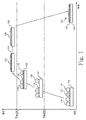
図1は、本発明の一実施形態に従う混成ソルダペーストを使用したリフロープロセスを図示する。この混成ソルダペーストはフラックス内に懸濁された第1合金ソルダ粒子118と第2合金ソルダ粒子115とを含んでいる。実施態様によっては、基材に対する、あるいは通常の基材の範囲に対する優れた反応化学特性に従って第2合金は選択される。混成ソルダペーストは基材124に適用される。(説明のため、フラックスは図面には図示しない)
FIG. 1 illustrates a reflow process using a hybrid solder paste according to one embodiment of the present invention. The hybrid solder paste includes first
リフロー中に、組立部品の温度は第2合金の融点Tm(B)を超えて上昇する。第2合金112は溶解し、基材124上および固体状態を保つ第1合金粒子118上に広がる。第2合金の優れた表面反応化学特性は基材124上での溶融ソルダ合金112のウェッティングを促すであろう。これで溶融第2合金112と基材124との間にIMC層109が形成される。従って、IMC層は主として当初のペースト内の第2合金115の量によって制御される。
During reflow, the temperature of the assembly rises above the melting point Tm (B) of the second alloy. The
さらに、第2合金は第1合金に対して良好な親和性を有するように設計される。この親和性は、(1)第1合金と第2合金との間の負の混合エンタルピーによるか、あるいは(2)第1合金および第2合金からの構成元素で構成される共晶相の形成によって決定できる。実施態様によっては、この親和性は溶融第2合金112内に第1合金118の一部が溶解する結果を招き、第1合金と第2合金の混成物106を形成する。
Furthermore, the second alloy is designed to have a good affinity for the first alloy. This affinity is either due to (1) the negative mixing enthalpy between the first alloy and the second alloy, or (2) the formation of a eutectic phase composed of constituent elements from the first alloy and the second alloy. Can be determined by. In some embodiments, this affinity results in the dissolution of a portion of the
温度が第1合金の融点Tm(A)を超えて上昇するにつれて第1合金は溶解を終結させ、第1合金と第2合金の溶液103を形成し、IMC層109をウェッティングする。組立部品がTm(A)を超えて維持された状態で、第2合金は溶液103から除去され、IMC層109を増加させ、溶融第1合金100を残す。実施態様によっては、IMC層109を形成するに加えて、第2合金からの余剰構成成分は第1合金からの構成成分と共にIMC内に取り込まれる。第1合金と第2合金との間の親和性はIMC層109上への第1合金100のウェッティングの改善に貢献し、結合強度を増強する。
As the temperature rises above the melting point Tm (A) of the first alloy, the first alloy terminates melting, forms a
組立部品が冷却されると、ソルダバンプ121または結合部が、IMC109に接着された基材124で形成され、固化した第1合金に接着される。固化後には、改善された接着インターフェースを備えた均質ソルダ結合部が達成されている。
When the assembly part is cooled, the
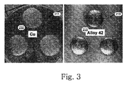
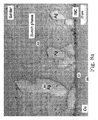
混成ソルダペーストの使用から得られるソルダ結合部は、1つのソルダ合金を含んだソルダペーストの使用の大きな改善を示し、その単一ソルダ合金が第1合金と第2合金の元素で構成される場合であっても改善される。図2は、それぞれCu基材200とAlloy42基材205の上の86.24重量%Bi10.02Ag3.74Sn+10重量%フラックスからなるソルダペーストを使用して形成されたソルダバンプ201と207を図示する。これらの結果が示すように、大きな脱ウェッティング202と206が1つ(単一)のソルダ合金の使用で発生する。一方、図3は、それぞれCu基材210とAlloy42基材215の上の84重量%Bi11Ag+6重量%Bi42Sn+10重量%フラックスからなる混成ソルダペーストを使用して形成されたソルダバンプ211と216を図示する。これらの結果が示すように、混成ソルダペーストの使用はほとんど、または全く視認できる脱ウェッティングを示さない。
Solder joints resulting from the use of a hybrid solder paste show a significant improvement in the use of a solder paste containing one solder alloy, where the single solder alloy is composed of elements of the first and second alloys Even better. FIG. 2 illustrates solder bumps 201 and 207 formed using a solder paste of 86.24 wt% Bi10.02Ag3.74Sn + 10 wt% flux on
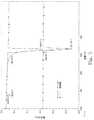
一実施形態においては、混成ソルダペーストは第1合金としてのBiAgと第2合金としてのSnSbを含んでいる。第2合金においてSnは、様々な基材とのBiに勝るその優れた反応化学特性のために選択されている。SnSbはBiAgよりも融点が低い。SnとBiは負の混合エンタルピーを示し、二元相図に従って広い組成物範囲に共晶相を形成する。SbとBiはまた負混合エンタルピーおよび相互無限溶解性も示す。リフロー中にSnSbが最初に溶解し、Sn含有IMC層を基材表面上に形成する。温度がBiAgの融点を超えると、ペースト内の全ての合金粉末は溶解する。BiとSn/Sbとの間の良好な親和性はSn含有IMC層上での溶融Biの良好な接着を保証する。さらに、第1合金内でのAgの存在はソルダ本体内に存在するAg3SnIMCに余剰Snを変換する。よって、最少の低温溶解BiSn相が残されるか、または全く低温溶解BiSn相は残らない。なぜなら、Snは(1)ソルダと金属基材との間にIMC層を形成し、(2)Ag3SnをBiAgソルダバンプ内部に形成することによって完全に消費されるからである。 In one embodiment, the hybrid solder paste includes BiAg as the first alloy and SnSb as the second alloy. In the second alloy, Sn has been selected for its excellent reaction chemistry over Bi with various substrates. SnSb has a lower melting point than BiAg. Sn and Bi exhibit a negative mixing enthalpy and form a eutectic phase over a wide composition range according to the binary phase diagram. Sb and Bi also exhibit negative mixing enthalpy and mutual infinite solubility. During reflow, SnSb is first dissolved to form a Sn-containing IMC layer on the substrate surface. When the temperature exceeds the melting point of BiAg, all the alloy powder in the paste is dissolved. Good affinity between Bi and Sn / Sb ensures good adhesion of molten Bi on the Sn-containing IMC layer. Furthermore, the presence of Ag in the first alloy converts surplus Sn into Ag3SnIMC present in the solder body. Thus, the least low temperature dissolved BiSn phase is left, or no low temperature dissolved BiSn phase remains. This is because Sn is completely consumed by (1) forming an IMC layer between the solder and the metal substrate and (2) forming Ag3Sn inside the BiAg solder bump.
図5は、84重量%Bi11Ag+6重量%Sn15Sb+10重量%フラックスの使用から得られる結合部のDSC曲線を図示する。最上部の曲線はセラミッククーポン上のリフロー後の熱流プロフィールを示す。138℃近辺のスパイクは第2合金の存在を示す。最下部の曲線はCuクーポン上のリフロー後のペーストの熱流プロフィールを示す。最下部の曲線でのこのスパイクの不在は、BiAg+SnSb系内の低温溶解相の消失を立証する。図6は、BiAg+SnAg系内の低温溶解相の消失を示す。図6の実験は、84重量%Bi11Ag+6重量%Sn3.5Ag+10重量%フラックスを図5で示すようにセラミッククーポンとCuクーポン上で使用した。図7は、BiAg+BiSn系内での消失を示す。図7の実験は、図5及び図6同様にセラミッククーポンとCuクーポン上で84重量%Bi11Ag+6重量%Bi42Sn+10重量%フラックスを使用した。図7では、セラミック上のソルダリフロー後の熱流プロフィールを示す最上部の曲線は低温溶解相の欠落を示す。これは、混成ソルダペースト内の反応剤Snの少量と、SnとAgとの間の高親和性とによるものであろうし、結果として、第2合金のSnが最終ソルダバンプ内のIMCに第1合金のAgの一部と共に取り込まれる結果となる。 FIG. 5 illustrates the DSC curve of the joint resulting from the use of 84 wt% Bi11Ag + 6 wt% Sn15Sb + 10 wt% flux. The top curve shows the heat flow profile after reflow on the ceramic coupon. Spikes around 138 ° C indicate the presence of the second alloy. The bottom curve shows the heat flow profile of the paste after reflow on the Cu coupon. The absence of this spike in the bottom curve demonstrates the disappearance of the low temperature dissolved phase in the BiAg + SnSb system. FIG. 6 shows the disappearance of the low temperature dissolution phase in the BiAg + SnAg system. The experiment of FIG. 6 used 84 wt% Bi11Ag + 6 wt% Sn3.5Ag + 10 wt% flux on the ceramic coupon and Cu coupon as shown in FIG. FIG. 7 shows the disappearance in the BiAg + BiSn system. The experiment of FIG. 7 used 84 wt% Bi11Ag + 6 wt% Bi42Sn + 10 wt% flux on the ceramic coupon and Cu coupon as in FIGS. In FIG. 7, the top curve showing the heat flow profile after solder reflow on the ceramic shows the lack of a cold melt phase. This may be due to the small amount of reactive agent Sn in the mixed solder paste and the high affinity between Sn and Ag, and as a result, the second alloy Sn is in the first alloy to the IMC in the final solder bump. Results in incorporation with a portion of the Ag.
図8aは、84重量%Bi11Ag+6重量%Sn3.5Ag+10重量%フラックスからなる混成ソルダペーストの使用から得られるソルダ結合部の顕微鏡図である。この実施例では、混成ソルダペーストがCuクーポン300に適用された。IMC301はCu300と第2合金との間に形成される。IMC301のサイズは主としてペースト内の第2合金の量に依拠する。図示の実施例では、6重量%の第2合金Sn3.5Agはたった数ミクロン厚のIMCとなった。ソルダ結合部の大部分はBiリッチ相302内のAg303で成る。150℃で2週間のエージング(寝かし)はIMC厚を大きくは増加させなかった。一方、BiとCuは中間金属を形成せず、IMC層がソルダと基材との間に存在しないため、Bi11Agのみが弱い結合(力)を形成する。
FIG. 8a is a micrograph of a solder joint resulting from the use of a hybrid solder paste consisting of 84 wt% Bi11Ag + 6 wt% Sn3.5Ag + 10 wt% flux. In this example, a hybrid solder paste was applied to the
本発明の一実施形態においては、混成ソルダペーストを設計する方法は、仕上げソルダ結合部の所望の特性に応じて第1合金を選択し、続いて、適用可能な基材と、選択された第1合金との親和性とに基づいて第2合金を選択することを含む。第1合金、第2合金およびフラックスの相対量は、所望のIMC層厚、要求される適用条件およびリフロープロセス、等々の条件に基づいて決定できる。IMC層厚はソルダペースト内の第2合金の量と、リフロープロフィールと、適用後のエージング条件とに関係する。許容可能なIMC層の厚みは異なる適用条件および異なるIMC組成によって変動できる。例えば、Cu6Sn5/Cu3SNのIMC層には10ミクロンがほぼ許容可能な厚みである。 In one embodiment of the present invention, a method of designing a hybrid solder paste selects a first alloy according to the desired properties of a finished solder joint, followed by an applicable substrate and a selected first Selecting the second alloy based on the affinity with the one alloy. The relative amounts of the first alloy, the second alloy and the flux can be determined based on conditions such as the desired IMC layer thickness, the required application conditions and the reflow process. The IMC layer thickness is related to the amount of the second alloy in the solder paste, the reflow profile, and the aging conditions after application. The acceptable IMC layer thickness can vary with different application conditions and different IMC compositions. For example, for a Cu6Sn5 / Cu3SN IMC layer, 10 microns is an acceptable thickness.
ペースト内の第2合金の量が増加するにつれて最終結合部には低温溶解相が残るであろう。もし第2合金の量がソルダペースト内で低下したら、所望のウェッティング性能は達成が困難になろう。第2合金の量が減少すると、良好なウェッティングには基材上に印刷されるか提供された、さらに多い総量のペーストの使用が必要となる。しかし、ペーストの全量の増加は、はんだ付けパッケージからの形状的制約に干渉するかもしれない。 As the amount of the second alloy in the paste increases, a cold melt phase will remain in the final bond. If the amount of the second alloy is reduced in the solder paste, the desired wetting performance will be difficult to achieve. As the amount of the second alloy decreases, good wetting requires the use of a higher total amount of paste printed or provided on the substrate. However, an increase in the total amount of paste may interfere with geometric constraints from the soldered package.
高温ソルダ適用のためには、第1合金は様々な高温溶解ソルダ合金から選択されなければならない。実施態様によっては、その固相線温度が258℃程度以上であるBiリッチ合金、すなわちBi−Ag、Bi−CuおよびBi−Ag−Cuが使用される。第2合金(追加物)は、様々な金属皮膜表面仕上げ面上でウェッティングして接着する優れた化学特性と、融解Biに対する良好な親和性とを示す合金から選択される。 For high temperature solder applications, the first alloy must be selected from a variety of high temperature melting solder alloys. In some embodiments, Bi-rich alloys having a solidus temperature of about 258 ° C. or higher, ie Bi—Ag, Bi—Cu, and Bi—Ag—Cu are used. The second alloy (additive) is selected from alloys that exhibit excellent chemical properties to wet and adhere on various metallized surface finishes and good affinity for molten Bi.
これらの実施形態において、第2合金はBiリッチ合金に先立って、あるいはそれと共に溶解し、続いて基材上を容易にウェッティングして接着するであろう。一方、Biと第2合金との間の良好な親和性は良好なウェッティングを提供するであろう。従って、Sn、Sn合金、InおよびIn合金が第2合金として選択される。選択された第2合金の融点に基づいて3つのグループが分類されている。グループAは、固相線温度が約230℃から250℃の追加合金、すなわちSn、Sn−Sb、Sn−Sb−X(X=Ag、Al、Au、Bi、Co、Cu、Ga、Ge、In、Mn、Ni、P、Pd、PtおよびZn)合金、等々を含む。グループBは、固相線温度が約200℃から230℃のソルダ合金であるSn−Ag、Sn−Cu、Sn−Ag−X(X=Al、Au、Bi、Co、Cu、Ga、Ge、In、Mn、Ni、P、Pd、Pt、SbおよびZn)並びにSn−Zn合金、等々を含む。グループCは、200℃未満の固相線温度であるソルダ合金、すなわちSn−Bi、Sn−In、Bi−In、In−Cu、In−AgおよびIn−Ag−X(X=Al、Au、Bi、Co、Cu、Ga、Ge、Mn、Ni、P、Pd、Pt、Sb、SnおよびZn)、Sn−Bi−X(X=Ag、Al、Au、Co、Cu、Ga、Ge、In、Mn、Ni、P、Pd、Pt、SbまたはZn)、Sn−In−X(X=Ag、Al、Au、Bi、Co、Cu、Ga、Ge、Mn、Ni、P、Pd、Pt、SbまたはZn)、およびBi−In−X(X=Ag、Al、Au、Co、Cu、Ga、Ge、Mn、Ni、P、Pd、Pt、SbまたはZn)合金、等々のソルダ合金を有する。これら合金において、Sn及び/又はInは合金系の反応剤である。 In these embodiments, the second alloy will dissolve prior to or with the Bi-rich alloy and will then be easily wetted and bonded onto the substrate. On the other hand, a good affinity between Bi and the second alloy will provide good wetting. Therefore, Sn, Sn alloy, In and In alloy are selected as the second alloy. Three groups are classified based on the melting point of the selected second alloy. Group A is an additional alloy with a solidus temperature of about 230 ° C. to 250 ° C., ie Sn, Sn—Sb, Sn—Sb—X (X = Ag, Al, Au, Bi, Co, Cu, Ga, Ge, In, Mn, Ni, P, Pd, Pt and Zn) alloys, and the like. Group B is a solder alloy having a solidus temperature of about 200 ° C. to 230 ° C., Sn—Ag, Sn—Cu, Sn—Ag—X (X = Al, Au, Bi, Co, Cu, Ga, Ge, In, Mn, Ni, P, Pd, Pt, Sb and Zn), Sn—Zn alloys, and the like. Group C is a solder alloy with a solidus temperature below 200 ° C., ie Sn—Bi, Sn—In, Bi—In, In—Cu, In—Ag and In—Ag—X (X = Al, Au, Bi, Co, Cu, Ga, Ge, Mn, Ni, P, Pd, Pt, Sb, Sn and Zn), Sn-Bi-X (X = Ag, Al, Au, Co, Cu, Ga, Ge, In) , Mn, Ni, P, Pd, Pt, Sb or Zn), Sn-In-X (X = Ag, Al, Au, Bi, Co, Cu, Ga, Ge, Mn, Ni, P, Pd, Pt, Sb or Zn), and Bi-In-X (X = Ag, Al, Au, Co, Cu, Ga, Ge, Mn, Ni, P, Pd, Pt, Sb or Zn) alloys, etc. . In these alloys, Sn and / or In are alloy-based reactants.
本発明の一実施形態においては、第1合金はBi−Ag系からの合金であり、約260℃以上の固相線温度を有する。一特定実施形態では、第1合金は0から20重量%のAgを含み、残りはBiである。さらに別の実施形態では、第1合金は2.6から15重量%のAgを含み、残りはBiである。 In one embodiment of the invention, the first alloy is an alloy from the Bi—Ag system and has a solidus temperature of about 260 ° C. or higher. In one particular embodiment, the first alloy comprises 0 to 20 wt% Ag with the balance being Bi. In yet another embodiment, the first alloy includes 2.6 to 15 wt% Ag with the balance being Bi.
本発明の第2実施形態においては、第1合金はBi−Cu系から選択され、約270℃以上の固相線温度を有する。一特定実施形態では、第1合金は0から5重量%のCuを含み、残りはBiである。さらに別な実施形態では、第1合金は0.2から1.5重量%のCuを含み、残りはBiである。 In the second embodiment of the present invention, the first alloy is selected from a Bi—Cu system and has a solidus temperature of about 270 ° C. or higher. In one particular embodiment, the first alloy comprises 0 to 5 wt% Cu with the balance being Bi. In yet another embodiment, the first alloy includes 0.2 to 1.5 weight percent Cu with the balance being Bi.
本発明の第3実施形態においては、第1合金はBi−Ag−Cu系から選択され、約258℃以上の固相線温度を有する。一特定実施形態では、第1合金は0から20重量%のAgと、0から5重量%のCuを含み、残りはBiである。さらに別な実施形態では、第1合金は2.6から15重量%のAgと、0.2から1.5重量%のCuを含み、残りはBiである。 In the third embodiment of the present invention, the first alloy is selected from the Bi—Ag—Cu system and has a solidus temperature of about 258 ° C. or higher. In one particular embodiment, the first alloy comprises 0 to 20 wt% Ag and 0 to 5 wt% Cu with the balance being Bi. In yet another embodiment, the first alloy includes 2.6 to 15 wt% Ag and 0.2 to 1.5 wt% Cu with the balance being Bi.
本発明の第4実施形態においては、第2合金はSn−Sb系から選択され、約231℃から約250℃の固形線温度を有する。一特定実施形態では、第2合金は0から20重量%のSbを含み、残りはSnである。さらに別な実施形態では、第2合金は0から15重量%のSbを含み、残りはSnである。 In a fourth embodiment of the invention, the second alloy is selected from the Sn—Sb system and has a solid line temperature of about 231 ° C. to about 250 ° C. In one particular embodiment, the second alloy includes 0 to 20 wt% Sb, with the remainder being Sn. In yet another embodiment, the second alloy includes 0 to 15 wt% Sb, with the remainder being Sn.
本発明の第5実施形態では、第2合金はSn−Sb−X(X=Ag,Al、Au、Bi、Co、Cu、Ga、Ge、In、Mn、Ni、P、Pd、PtおよびZn)を含み、約230℃から約250℃の固相線温度を有する。一特定実施形態では、第2合金は0から20重量%のSbと0から20重量%のXを含み、残りはSnである。さらに別な実施形態では、第2合金は0から10重量%のSbと0から5重量%のXを含み、残りはSnである。 In the fifth embodiment of the present invention, the second alloy is Sn—Sb—X (X = Ag, Al, Au, Bi, Co, Cu, Ga, Ge, In, Mn, Ni, P, Pd, Pt and Zn. And has a solidus temperature of about 230 ° C. to about 250 ° C. In one particular embodiment, the second alloy comprises 0 to 20 wt% Sb and 0 to 20 wt% X with the remainder being Sn. In yet another embodiment, the second alloy includes 0 to 10 wt% Sb and 0 to 5 wt% X with the remainder being Sn.
本発明の第6実施形態においては、第2合金はSn−Agを含み、約221℃以上の固相線温度を有する。一特定実施形態では、第2合金は0から10重量%のAgを含み、残りはSnである。別な実施形態では、第2合金は0から5重量%のAgを含み、残りはSnである。 In the sixth embodiment of the present invention, the second alloy includes Sn—Ag and has a solidus temperature of about 221 ° C. or higher. In one particular embodiment, the second alloy comprises 0 to 10 wt% Ag with the balance being Sn. In another embodiment, the second alloy comprises 0 to 5 wt% Ag with the balance being Sn.
本発明の第7実施形態においては、第2合金はSn−Cuを含み、約227℃以上の固相線温度を有する。一特定実施形態では、第2合金は0から5重量%のCuを含み、残りはSnである。別な実施形態では、第2合金は0から2重量%のCuを含み、残りはSnである。 In the seventh embodiment of the present invention, the second alloy includes Sn—Cu and has a solidus temperature of about 227 ° C. or higher. In one particular embodiment, the second alloy comprises 0 to 5 wt% Cu with the balance being Sn. In another embodiment, the second alloy includes 0 to 2 wt% Cu with the balance being Sn.
本発明の第8実施形態においては、第2合金はSn−Ag−X(X=Al、Au、Bi、Co、Cu、Ga、Ge、In、Mn、Ni、P、Pd、Pt、SbおよびZn)を含み、約216℃以上の固相線温度を有する。一特定実施形態では、第2合金は0から10重量%のAgと0から20重量%のXを含み、残りはSnである。別な実施形態では、第2合金は0から5重量%のAgと0から5重量%のXを含み、残りはSnである。 In the eighth embodiment of the present invention, the second alloy is Sn—Ag—X (X = Al, Au, Bi, Co, Cu, Ga, Ge, In, Mn, Ni, P, Pd, Pt, Sb and Zn) and has a solidus temperature of about 216 ° C. or higher. In one particular embodiment, the second alloy comprises 0 to 10 wt% Ag and 0 to 20 wt% X with the balance being Sn. In another embodiment, the second alloy comprises 0 to 5 wt% Ag and 0 to 5 wt% X with the balance being Sn.
本発明の第9実施形態においては、第2合金はSn−Znを含み、約200℃以上の固相線温度を有する。一特定実施形態では、第2合金は0から20重量%のZnを含み、残りはSnである。別な実施形態では、第2合金は0から9重量%のZnを含み、残りはSnである。 In the ninth embodiment of the present invention, the second alloy contains Sn—Zn and has a solidus temperature of about 200 ° C. or higher. In one particular embodiment, the second alloy comprises 0 to 20 wt% Zn with the remainder being Sn. In another embodiment, the second alloy includes 0 to 9 wt% Zn with the balance being Sn.
本発明の第10実施形態においては、第2合金はBi−Sn合金を含み、約139℃以上の固相線温度を有する。一特定実施形態では、第2合金は8から80重量%のSnを含み、残りはBiである。別な実施形態では、第2合金は30から60重量%のSnを含み、残りはBiである。 In the tenth embodiment of the present invention, the second alloy includes a Bi—Sn alloy and has a solidus temperature of about 139 ° C. or higher. In one particular embodiment, the second alloy includes 8 to 80 wt% Sn with the balance being Bi. In another embodiment, the second alloy includes 30 to 60 wt% Sn with the balance being Bi.
本発明の第11実施形態においては、第2合金はSn−In合金を含み、約120℃以上の固相線温度を有する。一特定実施形態では、第2合金は0から80重量%のInを含み、残りはSnである。別な実施形態では、第2合金は30から50重量%のInを含み、残りはSnである。 In the eleventh embodiment of the present invention, the second alloy includes a Sn—In alloy and has a solidus temperature of about 120 ° C. or higher. In one particular embodiment, the second alloy comprises 0 to 80 wt% In and the rest is Sn. In another embodiment, the second alloy includes 30 to 50 weight percent In and the remainder is Sn.
本発明の第12実施形態においては、第2合金はBi−In合金を含み、約100℃から約200℃の固相線温度を有する。一特定実施形態では、第2合金は0から50重量%のInを含み、残りはBiである。別な実施形態では、第2合金は20から40重量%のInを含み、残りはBiである。 In a twelfth embodiment of the present invention, the second alloy includes a Bi—In alloy and has a solidus temperature of about 100 ° C. to about 200 ° C. In one particular embodiment, the second alloy contains 0 to 50 wt% In with the remainder being Bi. In another embodiment, the second alloy includes 20 to 40 weight percent In and the balance is Bi.
本発明の第13実施形態においては、第2合金はIn−Cu合金を含み、約100℃から約200℃の固相線温度を有する。一特定実施形態では、第2合金は0から10重量%のCuを含み、残りはInである。別な実施形態では、第2合金は0から5重量%のCuを含み、残りはInである。 In a thirteenth embodiment of the present invention, the second alloy includes an In—Cu alloy and has a solidus temperature of about 100 ° C. to about 200 ° C. In one particular embodiment, the second alloy comprises 0 to 10 wt% Cu with the balance being In. In another embodiment, the second alloy includes 0 to 5 weight percent Cu with the balance being In.
本発明の第14実施形態においては、第2合金はIn−Ag合金を含み、約100℃から約200℃の固相線温度を有する。一特定実施形態では、第2合金は0から30重量%のAgを含み、残りはInである。別な実施形態では、第2合金は0から10重量%のAgを含み、残りはInである。 In a fourteenth embodiment of the invention, the second alloy comprises an In—Ag alloy and has a solidus temperature of about 100 ° C. to about 200 ° C. In one particular embodiment, the second alloy comprises 0 to 30 wt% Ag with the remainder being In. In another embodiment, the second alloy contains 0 to 10 wt% Ag with the remainder being In.
第15実施形態では、第2合金はIn−Ag−X(X=Al、Au、Bi、Co、Cu、Ga、Ge、Mn、Ni、P、Pd、Pt、Sb、SnおよびZn)を含み、約100℃から200℃の固相線温度を有する。一特定実施形態では、第2合金は0から20重量%のAgと0から20重量%のXを含み、残りはInである。別な実施形態では、第2合金は0から10重量%のAgと0から5重量%のXを含み、残りはInである。 In the fifteenth embodiment, the second alloy includes In—Ag—X (X = Al, Au, Bi, Co, Cu, Ga, Ge, Mn, Ni, P, Pd, Pt, Sb, Sn, and Zn). Having a solidus temperature of about 100 ° C to 200 ° C. In one particular embodiment, the second alloy comprises 0 to 20 wt% Ag and 0 to 20 wt% X, with the remainder being In. In another embodiment, the second alloy includes 0 to 10 wt% Ag and 0 to 5 wt% X, with the remainder being In.
本発明の更なる実施例は混成ソルダペーストを製造する方法を提供する。実施形態によっては、第1合金の粒子が形成され、第2合金の粒子が形成される。第1合金と第2合金の粒子はその後にフラックスと混合されてソルダペーストが形成される。最終ペーストは、第1合金粉末、第2合金粉末および残りのフラックスを含んでいる。実施形態によっては、第1合金粒子は少なくとも約260℃の固相線温度を有した合金製である。 A further embodiment of the present invention provides a method for producing a hybrid solder paste. In some embodiments, particles of the first alloy are formed and particles of the second alloy are formed. The particles of the first alloy and the second alloy are then mixed with the flux to form a solder paste. The final paste includes the first alloy powder, the second alloy powder, and the remaining flux. In some embodiments, the first alloy particles are made of an alloy having a solidus temperature of at least about 260 ° C.
さらに別な実施形態では、第2合金は、固相線温度が約230℃と約250℃の間である合金、固相線温度が約200℃と約230℃の間である合金、又は、固相線温度が約200℃未満である合金とを含んでいる。実施形態によっては、ペーストは約60重量%と約92重量%の間の第1合金粉末を含んでおり、第2合金粉末の量は0%を超えるが12重量%以下であり、残りはフラックスである。さらに別な実施形態では、第2合金粉末は、2重量%と10重量%の間の混成ソルダペーストである。 In yet another embodiment, the second alloy is an alloy having a solidus temperature between about 230 ° C. and about 250 ° C., an alloy having a solidus temperature between about 200 ° C. and about 230 ° C., or And alloys having a solidus temperature of less than about 200 ° C. In some embodiments, the paste includes between about 60% and about 92% by weight of the first alloy powder, the amount of the second alloy powder is greater than 0% but not more than 12% by weight, with the remainder being flux It is. In yet another embodiment, the second alloy powder is a mixed solder paste between 2% and 10% by weight.
一特定実施形態では、第1合金は、Bi−Ag合金、Bi−Cu合金、又はBi−Ag−Cu合金を含んでいる。さらに別な実施形態では、約230℃から約250℃の固相線温度を有した合金は、Sn合金、Sn−Sb合金、又はSn−Sb−X(X=Ag、Al、Au、Bi、Co、Cu、Ga、Ge、In、Mn、Ni、P、Pd、PtおよびZn)合金を含んでいる。別の実施形態では、約200℃から約230℃の固相線温度を有した合金は、Sn−Ag合金、Sn−Cu合金、Sn−Ag−X(X=Al、Au、Bi、Co、Cu、Ga、Ge、In、Mn、Ni、P、Pd、Pt、SbおよびZn)合金、またはSn−Zn合金を含んでいる。さらに別な実施形態では、約200℃未満の固相線温度を有した合金は、Sn−Bi合金、Sn−In合金、またはBi−In合金を含んでいる。 In one particular embodiment, the first alloy includes a Bi—Ag alloy, a Bi—Cu alloy, or a Bi—Ag—Cu alloy. In yet another embodiment, the alloy having a solidus temperature of about 230 ° C. to about 250 ° C. is Sn alloy, Sn—Sb alloy, or Sn—Sb—X (X = Ag, Al, Au, Bi, Co, Cu, Ga, Ge, In, Mn, Ni, P, Pd, Pt and Zn) alloys. In another embodiment, the alloy having a solidus temperature of about 200 ° C. to about 230 ° C. is Sn—Ag alloy, Sn—Cu alloy, Sn—Ag—X (X = Al, Au, Bi, Co, Cu, Ga, Ge, In, Mn, Ni, P, Pd, Pt, Sb and Zn) alloys or Sn—Zn alloys are included. In yet another embodiment, the alloy having a solidus temperature less than about 200 ° C. includes a Sn—Bi alloy, a Sn—In alloy, or a Bi—In alloy.
さらに別な実施形態では、第2合金粉末は、複数の合金粉末を含んだ粉末を含んでいる。例えば、第2合金粉末は、ここで説明した合金から選択された異なる合金の混合物を含むことができる。実施形態によっては、混成ソルダペースト内の第1合金と第2合金の相対量はソルダ適用形態に従って決定される。実施形態によっては、ペースト内の第2ソルダ合金の量が所定の閾値を超えて増加すると、最終ソルダ結合部内にいくらかの低温溶解相を維持する確率は増加するであろう。場合によっては、ペースト内の第2ソルダ合金の量が所定の閾値を下回ると、基材へのウェッティングは減少するであろう。一実施形態では、ペースト内の第2ソルダ合金の量は、低温溶解相がリフロー後に高温溶解IMCに完全に変換できるように決定される。別な実施形態では、ペースト内の第2合金は0重量%を超える量と約12重量%未満の量との間で変動する。一特定実施形態では、ペースト内の第2合金は約2重量%を超えるが、約10重量%未満である。 In still another embodiment, the second alloy powder includes a powder including a plurality of alloy powders. For example, the second alloy powder can include a mixture of different alloys selected from the alloys described herein. In some embodiments, the relative amounts of the first alloy and the second alloy in the hybrid solder paste are determined according to the solder application form. In some embodiments, as the amount of the second solder alloy in the paste increases beyond a predetermined threshold, the probability of maintaining some low temperature melt phase in the final solder joint will increase. In some cases, wetting to the substrate will decrease when the amount of the second solder alloy in the paste falls below a predetermined threshold. In one embodiment, the amount of the second solder alloy in the paste is determined so that the low temperature melt phase can be completely converted to high temperature melt IMC after reflow. In another embodiment, the second alloy in the paste varies between an amount greater than 0 wt% and an amount less than about 12 wt%. In one particular embodiment, the second alloy in the paste is greater than about 2% by weight but less than about 10% by weight.
様々な通常の不純物すなわち少量の異なる元素に加えて、Snの反応特性が維持される限り他の元素を加えるか、合金内に取り込むことができる。 In addition to various normal impurities, a small amount of different elements, other elements can be added or incorporated into the alloy so long as the reaction characteristics of Sn are maintained.
実施形態によっては、混成ソルダペーストでのハンダ付けに使用されるリフロープロフィールは、第1合金の融点を超える温度に素早く熱せられるよう設計される。この場合には、低温での短い浸し時間がSn等の反応剤を基材側に素早く流させ、半固状溶解プールではなく完全溶解プール内で基材と反応させる。第1合金と第2合金の両方の溶解は、溶融ソルダから基材および部品への第2合金元素の拡散、並びに表面上への“沈め込み”を促すであろう。 In some embodiments, the reflow profile used for soldering with the hybrid solder paste is designed to be quickly heated to a temperature above the melting point of the first alloy. In this case, a short immersion time at a low temperature causes a reactant such as Sn to flow quickly to the substrate side, and reacts with the substrate in the complete dissolution pool rather than the semi-solid dissolution pool. The dissolution of both the first alloy and the second alloy will facilitate the diffusion of the second alloy element from the molten solder into the substrate and parts, as well as “sinking” onto the surface.
Example(実施例)
ここで説明する範囲をカバーする様々な混成合金粉末ソルダペーストが、ソルダ性能の確認のために試験された。
Example
Various hybrid alloy powder solder pastes covering the ranges described herein were tested to confirm solder performance.
表1は、Bi11AgまたはBi2.6Agを含んだ第1合金と、Sn10Ag25SbまたはSn10Ag10Sbを含んだ第2合金と、フラックスとを使用して作製された例示的混成ソルダペーストの組成を説明する。 Table 1 illustrates the composition of an exemplary hybrid solder paste made using a first alloy containing Bi11Ag or Bi2.6Ag, a second alloy containing Sn10Ag25Sb or Sn10Ag10Sb, and a flux.

表2は、Bi11Agを含んだ第1合金と、Sn3.8Ag0.7Cu、Sn3.5Ag、Sn0.7CuまたはSn9Znを含んだ第2合金と、フラックスとを使用して作製された例示的混成ソルダペーストの組成を説明する。 Table 2 shows an exemplary hybrid solder paste made using a first alloy containing Bi11Ag, a second alloy containing Sn3.8Ag0.7Cu, Sn3.5Ag, Sn0.7Cu, or Sn9Zn, and a flux. The composition of is described.
表3は、Bi11Agを含んだ第1合金と、Bi42Sn、Bi33InまたはIn48Snを含んだ第2合金と、フラックスとを使用して作製された例示的混成ソルダペーストの組成を説明する。 Table 3 illustrates the composition of an exemplary hybrid solder paste made using a first alloy containing Bi11Ag, a second alloy containing Bi42Sn, Bi33In or In48Sn, and a flux.
表1、表2および表3によって説明したそれぞれのペーストが準備され、3穴ステンレス鋼ステンシルを使用してクーポン上に印刷された。Cu、Ni、Alloy42およびアルミナのクーポンが使用された。それぞれのペーストがそれぞれのクーポンに印刷された。穴は1/4インチ(約0.635cm)径であった。印刷されたクーポンは混成合金粉末ソルダペースト用に設計されているプロフィールを備えたリフローオーブンを介してリフローされた。リフローは、380℃、400℃および420℃の3域リフローオーブン内で、N2雰囲気下、ベルト速度13インチ(約33cm)/分で実施された。
Each paste described by Table 1, Table 2 and Table 3 was prepared and printed on the coupon using a 3 hole stainless steel stencil. Cu, Ni,
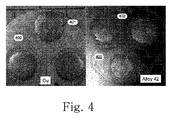
CuとNiのクーポン上のウェッティング性能は視覚的に検査された。混成ソルダ合金の全てが、単独BiAgソルダペーストと比較して改善されたウェッティング性能を示した。図3と図4は典型的な結果を表わす写真である。図3は、84重量%Bi11Ag+6重量%Bi42Sn+10重量%フラックスからなる混成合金粉末ソルダの1例のウェッティング性能を示す。左側の画像はCuクーポン上でリフローしたペーストを示し、右側の画像はAlloy42クーポン上でリフローしたペーストを示す。図4は、84重量%Bi11Ag+6重量%Bi52In48Sn+10重量%フラックスからなる混成合金粉末ソルダペーストの1例のウェッティング性能を示す。左側の画像はCuクーポン400上でリフローしたペースト401を示し、右側の画像は、Alloy42Cuクーポン405上でリフローしたペースト402を示す。
The wetting performance on Cu and Ni coupons was visually inspected. All of the hybrid solder alloys showed improved wetting performance compared to the single BiAg solder paste. 3 and 4 are photographs showing typical results. FIG. 3 shows an example of the wetting performance of a hybrid alloy powder solder composed of 84 wt% Bi11Ag + 6 wt% Bi42Sn + 10 wt% flux. The left image shows the reflowed paste on the Cu coupon, and the right image shows the reflowed paste on the
リフローしたソルダボールはDSC試験のためにアルミナクーポンから剥離された。Cuクーポン上とNiクーポン上に形成されたソルダバンプもDSC試験のためにパンチで除去された。10℃/分の加熱速度で示差走査熱量計を使用してDSC測定が実施された。代表的なDSC曲線は図5から図7に示されている。図5は、84重量%Bi11Ag+6重量%Sn15Sb+10重量%フラックスの使用で得られた結合部のDSC曲線を示す。最上部の曲線はセラミッククーポン上のリフロー後の熱流プロフィールを図示する。約138℃でのスパイクは第2合金の存在を示す。最下部の曲線はCuクーポン上のリフロー後のペーストの熱流プロフィールを示す。最下部の曲線でのこのスパイクの不在はBiAg+SnSb系内の低温溶解相の消失を確認する。図6は、BiAg+SnAg系内の低温溶解相の消失を示す。図6の実験は、図5でのように、セラミッククーポン上とCuクーポン上での84重量%Bi11Ag+6重量%Sn3.5Ag+10重量%フラックスを使用した。図7は、BiAg+BiSn系での消失を示す。図7の実験は、図5及び図6でのように、セラミッククーポン上とCuクーポン上での84重量%Bi11Ag+6重量%Bi42Sn+10重量%フラックスを使用した。図7において、セラミック上でのソルダリフロー後の熱流プロフィールを図示する最上部の曲線は低温溶解相の欠落を示す。これは、SnとAgとの間の高親和性によるものであろうし、第2合金のSnは最終ソルダバンプ内のIMC内に取り込まれる結果となろう。 The reflowed solder balls were peeled from the alumina coupon for DSC testing. Solder bumps formed on the Cu coupon and Ni coupon were also removed with a punch for DSC testing. DSC measurements were performed using a differential scanning calorimeter at a heating rate of 10 ° C / min. Representative DSC curves are shown in FIGS. FIG. 5 shows the DSC curve for the joint obtained using 84 wt% Bi11Ag + 6 wt% Sn15Sb + 10 wt% flux. The top curve illustrates the heat flow profile after reflow on the ceramic coupon. A spike at about 138 ° C indicates the presence of the second alloy. The bottom curve shows the heat flow profile of the paste after reflow on the Cu coupon. The absence of this spike in the bottom curve confirms the disappearance of the low temperature dissolved phase in the BiAg + SnSb system. FIG. 6 shows the disappearance of the low temperature dissolution phase in the BiAg + SnAg system. The experiment of FIG. 6 used 84 wt% Bi11Ag + 6 wt% Sn3.5Ag + 10 wt% flux on the ceramic coupon and Cu coupon as in FIG. FIG. 7 shows the disappearance in the BiAg + BiSn system. The experiment of FIG. 7 used 84 wt% Bi11Ag + 6 wt% Bi42Sn + 10 wt% flux on the ceramic coupon and Cu coupon, as in FIGS. In FIG. 7, the top curve illustrating the heat flow profile after solder reflow on the ceramic shows the lack of a low temperature dissolved phase. This may be due to the high affinity between Sn and Ag, and Sn in the second alloy will result in incorporation into the IMC in the final solder bump.
サンプルの断面は、ソルダバンプとCuクーポンまたはNiクーポンとの間のインターフェース(界面)でのIMC厚を決定するために画像化された。代表的な画像が図8に示されている。図8aは、Cuクーポン上で84重量%Bi11Ag+6重量%Sn3.5Ag+10重量%フラックスを使用したソルダバンプの断面である。図8bは、Niクーポン上で同じソルダペーストを使用したソルダバンプの断面である。これら結果が示すように、IMC層厚は両クーポン上で数μmに規制された。 A cross section of the sample was imaged to determine the IMC thickness at the interface between the solder bump and the Cu coupon or Ni coupon. A representative image is shown in FIG. FIG. 8a is a cross-section of a solder bump using 84 wt% Bi11Ag + 6 wt% Sn3.5Ag + 10 wt% flux on a Cu coupon. FIG. 8b is a cross section of a solder bump using the same solder paste on a Ni coupon. As these results show, the IMC layer thickness was regulated to a few μm on both coupons.
実施例においては、第2ソルダ合金は、0重量%を超え40重量%までのSb、0重量%を超え40重量%までのSn、およびBiで成るBi−Sb−Sn合金である。 In an embodiment, the second solder alloy is a Bi—Sb—Sn alloy consisting of greater than 0 wt% to 40 wt% Sb, greater than 0 wt% to 40 wt% Sn, and Bi.
実施例においては、第2ソルダ合金はBi−Sb−Sn−X合金であり、ここでXは、Ag、Al、Au、Co、Cu、Ga、Ge、In、Mn、Ni、P、Pd、PtまたはZnである。これら実施例の実施において、Bi−Sb−Sn−X合金は、0重量%を超え40重量%までのSb、0重量%を超え40重量%までのSn、0重量%を超え5重量%までのX、およびBiで成る。 In an embodiment, the second solder alloy is a Bi—Sb—Sn—X alloy, where X is Ag, Al, Au, Co, Cu, Ga, Ge, In, Mn, Ni, P, Pd, Pt or Zn. In the implementation of these examples, the Bi-Sb-Sn-X alloy is composed of more than 0% to 40% Sb, more than 0% to 40% Sn, more than 0% to 5% by weight. X and Bi.
実施例においては、第1ソルダ合金は、Bi−Ag−Y合金、Bi−Cu−Y合金、またはBi−Ag−Cu−Y合金であり、Yは、Al、Au、Co、Ga、Ge、In、Mn、Ni、P、Pd、Pt、Sb、SnまたはZnである。これら実施例の実施において、Yは、第1ソルダ合金の0重量%を超え5重量%までの範囲にある。 In an embodiment, the first solder alloy is a Bi—Ag—Y alloy, a Bi—Cu—Y alloy, or a Bi—Ag—Cu—Y alloy, where Y is Al, Au, Co, Ga, Ge, In, Mn, Ni, P, Pd, Pt, Sb, Sn, or Zn. In the implementation of these examples, Y is in the range of greater than 0% to 5% by weight of the first solder alloy.
さらなる実施例においては、ソルダペーストは、さらに高い重量%の第2合金粉末、さらに低い重量%の第1合金粉末、またはそれらいくらかの組み合わせで成る。そのような1実施例では、ソルダペーストは、44重量%と60重量%未満の第1合金粉末と、0重量%を超え48重量%未満の第2合金粉末と、0重量%と15重量%の間のフラックスで成る。この実施例の1特定形態では、第2合金粉末の量は、2重量%を超え40重量%未満であってもよい。 In further embodiments, the solder paste comprises a higher weight percent second alloy powder, a lower weight percent first alloy powder, or some combination thereof. In one such embodiment, the solder paste comprises 44 wt% and less than 60 wt% of the first alloy powder, greater than 0 wt% and less than 48 wt% of the second alloy powder, 0 wt% and 15 wt%. Consisting of a flux between. In one particular form of this example, the amount of the second alloy powder may be greater than 2 wt% and less than 40 wt%.
別なそのような実施例では、ソルダペーストは、44重量%と87重量%の間の第1ソルダ合金粉末と、13重量%と48重量%の間の第2ソルダ合金粉末と、0重量%と15重量%の間のフラックスで成る。この実施例の1特定形態では、第2合金粉末の量は26重量%と40重量%の間であってもよい。 In another such embodiment, the solder paste comprises between 44 wt% and 87 wt% first solder alloy powder, between 13 wt% and 48 wt% second solder alloy powder, and 0 wt%. And 15% by weight flux. In one particular form of this embodiment, the amount of the second alloy powder may be between 26% and 40% by weight.
これら別実施例では、さらに高い重量%の第2合金粉末、さらに低い重量%の第1合金粉末、またはその組み合わせは、ソルダペーストの均質性を高める。この改善された均質性は混成合金ソルダペーストをさらに小さな結合部の形成に適用することを可能にし、少なくとも、たった0.2mm径の結合部の接着であろうがウェッティングと高温性能の両方を提供する。さらに、ソルダ合金粉末のこの組み合わせは、リフロー後のさらに高温なソルダ結合部温度さえも可能にする。例えば、そのような一形態においては、形成された結合部の再溶解温度は270℃を超えることができる。別なそのような形態では、形成された結合部の再溶解温度は280℃まで、あるいはそれ以上になり得る。 In these alternative embodiments, a higher weight percent of the second alloy powder, a lower weight percent of the first alloy powder, or a combination thereof increases the homogeneity of the solder paste. This improved homogeneity allows the hybrid alloy solder paste to be applied to the formation of even smaller joints, at least for both wetting and high temperature performance, whether bonding of just 0.2 mm diameter joints. provide. Furthermore, this combination of solder alloy powders allows even higher solder joint temperatures after reflow. For example, in one such form, the remelting temperature of the formed bond can exceed 270 ° C. In another such form, the remelting temperature of the formed bond can be up to 280 ° C. or higher.
以上、本発明の様々な実施形態/実施例を説明してきたが、それらは例示として提供されただけであり、限定を意図したものではないことは理解されるべきである。同様に、様々な図面が本発明の例示的な構成またはその他の形態を図示するが、それらは本発明に含まれることができる特徴と機能性の理解を助けるために為されている。本発明は図示および説明された構成や形態に限定されず、望ましい特徴は様々な別構成および別形態を活用しても実施が可能である。事実、当業界の専門家には、本発明の望ましい特徴を実施するために、代替の機能的、論理的または物理的な分割および形態がいかに利用できるかは明らかであろう。また、ここで説明したもの以外の多数の異なる構成成分が様々な分割形態に適用できる。加えて、フロー図、運用の説明および方法クレーム(請求項)に関して、そこで実施ステップが提供されている順序は、特にその他に言及がない限り、様々な実施例が、明記された機能性を同一順序で実施すべく実施されることを要求しない。 Although various embodiments / examples of the present invention have been described above, it should be understood that they have been provided by way of example only and are not intended to be limiting. Similarly, the various drawings illustrate exemplary configurations or other forms of the invention, which are intended to assist in understanding the features and functionality that may be included in the invention. The present invention is not limited to the configurations and configurations shown and described, and desirable features can be implemented using various other configurations and configurations. In fact, it will be apparent to those skilled in the art how alternative functional, logical or physical divisions and forms can be utilized to implement the desired features of the present invention. In addition, many different components other than those described here can be applied to various division forms. In addition, with respect to flow diagrams, operational descriptions, and method claims (claims), the order in which the implementation steps are provided therein, unless otherwise noted, the various embodiments have the same specified functionality. Does not require to be performed in order.
本発明は様々な代表的実施例および態様によって上述されているが、1以上の個別の実施例で説明されている様々な特徴、形態および機能性は、説明されているそれらの特定実施例での適用性に限定されず、具体的に説明されていようがいまいが、そのような特徴が説明されている実施例の一部であると説明されていようがいまいが、単独または様々な組み合わせで本発明の他の実施例にも適用が可能であることは理解されるべきである。よって、本発明の広がりと範囲はいかなる上述の代表的な実施例に限定されるべきではない。 Although the present invention has been described above by various exemplary embodiments and aspects, the various features, forms and functionality described in one or more individual embodiments are not limited to those specific embodiments described. It is not limited to the applicability of the invention, whether specifically described, or whether such features are part of the described embodiment, either alone or in various combinations. It should be understood that other embodiments of the present invention are applicable. Accordingly, the breadth and scope of the present invention should not be limited to any of the above-described exemplary embodiments.
本明細書で使用されている用語および表現、並びにそれらの変形は、その他が特に明示的に述べられていなければ、限定されているものではなく開かれた意味である。その例として、“含む”なる語は、“限定なく含む”等を意味し、用語“例”は説明している物の代表例を提供するものであり、その枯渇的あるいは限定されたリストを提供するためのものではなく、特に数に言及されていないものは、“少なくとも1つ”、“1以上”等の意味であり、“従来的”、“伝統的”、“通常の”、“標準的”、“知られた”およびその類似表現は、所定の期間または所定の時期に利用可能な物に限定されると理解されるべきでなく、現在または将来の任意のときに利用が可能な、または知られている普通、伝統的、通常または標準的な技術を網羅すると読まれるべきである。同様に、この明細書が当該分野の専門家に明らかであるか知られた技術に言及する場合には、そのような技術は、現在または将来の任意のときに専門家に明らかであるか知られているものを網羅する。 The terms and expressions used herein, and their variations, unless otherwise expressly stated, are open-ended and not limiting. For example, the term “includes” means “including without limitation”, etc., and the term “example” provides a representative example of what is being described, including a depleted or limited list thereof. What is not intended to be provided, and what is not specifically mentioned in the number, means “at least one”, “one or more”, etc., “conventional”, “traditional”, “normal”, “ “Standard”, “known” and similar expressions are not to be understood as being limited to what is available at a given time or at a given time, but can be used at any time, now or in the future It should be read to cover any known, ordinary, traditional, ordinary or standard techniques. Similarly, when this specification refers to techniques that are obvious or known to a specialist in the field, such techniques are known or known to the expert at any time, now or in the future. It covers what is being done.
“1以上”、“少なくとも”、“限定されない”等々の用語は、広がりを持たせる用語が不在である場合に、それより狭い場合が想定されているか必要とされているということを意味しているとは理解されるべきではない。用語“モジュール”の使用は、モジュールの一部として説明されているか請求されている構成成分あるいは機能性が全て共通のパッケージ内に収まるように設計されているとは意味しない。事実、モジュールの様々な構成要素は、制御ロジックであろうが他の構成要素であろうが、1つのパッケージ内で組み合わせが可能であり、あるいは別々に維持が可能であり、さらに複数のグループまたはパッケージに、または複数の位置に別々に配分することが可能である。 Terms such as “one or more”, “at least”, “non-limiting”, etc. mean that if a broadening term is absent, a narrower case is envisaged or required. It should not be understood. The use of the term “module” does not mean that all components or functionality described or claimed as part of the module are designed to fit within a common package. In fact, the various components of the module, whether control logic or other components, can be combined in one package or can be maintained separately, and can be grouped or grouped together. It is possible to distribute to the package or to multiple locations separately.
加えて、ここに記載する様々な実施例は代表的なブロック図、フローチャート、その他の図の形態で説明されている。本明細書を読んだ当該分野の専門家には明らかであろうが、説明および図解されている実施例およびそれらの様々な変形は、説明されている例に限定されることなく実施が可能である。例えば、ブロック図およびそれらに付随する説明は、特定の構成または形態を必須とするものと理解されるべきではない。 Additionally, the various embodiments described herein are described in the form of representative block diagrams, flowcharts, and other diagrams. As will be apparent to those skilled in the art upon reading this specification, the embodiments described and illustrated, and various variations thereof, can be practiced without limitation to the described embodiments. is there. For example, block diagrams and the accompanying description should not be construed as requiring a particular configuration or configuration.
図2中の「Dewetting」とは、脱ウェッティング(または、非濡れ)。
図2,3,4中の「Alloy 42」は、合金42。
図8a,8bの「Solder」は、ソルダ(はんだ)。
「Bi−rich phase」は、Biリッチ相。
「IMC」は、金属間化合物。
“Dewetting” in FIG. 2 is dewetting (or non-wetting).
“
“Solder” in FIGS. 8a and 8b is solder.
“Bi-rich phase” is a Bi-rich phase.
“IMC” is an intermetallic compound.
Claims (32)
44重量%から60重量%未満の第1ソルダ合金粉末の量と、
0重量%を超え、48重量%までの第2ソルダ合金粉末の量と、
フラックスとからなり、
前記第1ソルダ合金粉末は、260℃を超える固相線温度を有した第1ソルダ合金を含んでおり、
前記第2ソルダ合金粉末は、250℃未満の固相線温度を有した第2ソルダ合金を含んでいる、ソルダペースト。 Solder paste (solder paste)
An amount of first solder alloy powder of 44 wt% to less than 60 wt%;
An amount of second solder alloy powder of greater than 0% by weight and up to 48% by weight;
Consisting of flux,
The first solder alloy powder includes a first solder alloy having a solidus temperature exceeding 260 ° C.,
The second solder alloy powder is a solder paste containing a second solder alloy having a solidus temperature of less than 250 ° C.
0重量%を超え20重量%までのAgで残り部分はBiを含むか、
0重量%を超え5重量%までのCuで残り部分はBiを含むか、あるいは、
0重量%を超え20重量%までのAgおよび0重量%を超え5重量%までのCuで残り部分はBiを含んでいる、請求項1記載のソルダペースト。 The first solder alloy is
The remaining part contains Bi with an Ag exceeding 0% by weight up to 20% by weight,
More than 0 wt.% And up to 5 wt.% Cu with the balance containing Bi, or
The solder paste according to claim 1, wherein more than 0% by weight of Ag and 20% by weight of Ag and more than 0% by weight of up to 5% by weight of Cu, with the remainder comprising Bi.
2.6重量%から15重量%のAgで残り部分はBiを含むか、
0.2重量%から1.5重量%のCuで残り部分はBiを含むか、あるいは、
2.6重量%から15重量%のAgおよび0.2重量%から1.5重量%のCuで残り部分はBiを含んでいる、請求項1記載のソルダペースト。 The first solder alloy is
2.6% to 15% by weight of Ag with the remainder containing Bi
0.2 wt% to 1.5 wt% Cu with the balance containing Bi, or
The solder paste according to claim 1, wherein 2.6% to 15% by weight of Ag and 0.2% to 1.5% by weight of Cu, with the remainder containing Bi.
44重量%と87重量%の間の第1ソルダ合金粉末の量と、
13重量%と48重量%の間の第2ソルダ合金粉末の量と、
フラックスとからなり、
前記第1ソルダ合金粉末は、260℃を超える固相線温度を有した第1ソルダ合金を含んでおり、
前記第2ソルダ合金粉末は、250℃未満の固相線温度を有した第2ソルダ合金を含んでいるソルダペースト。 Solder paste (solder paste)
An amount of first solder alloy powder between 44 wt% and 87 wt%;
An amount of second solder alloy powder between 13% and 48% by weight;
Consisting of flux,
The first solder alloy powder includes a first solder alloy having a solidus temperature exceeding 260 ° C.,
The second solder alloy powder is a solder paste containing a second solder alloy having a solidus temperature of less than 250 ° C.
0重量%を超え20重量%までのAgで残り部分はBiを含むか、
0重量%を超え5重量%までのCuで残り部分はBiを含むか、あるいは、
0重量%を超え20重量%までのAgおよび0重量%を超え5重量%までのCuで残り部分はBiを含んでいる、請求項15記載のソルダペースト。 The first solder alloy is
The remaining part contains Bi with an Ag exceeding 0% by weight up to 20% by weight,
More than 0 wt.% And up to 5 wt.% Cu with the balance containing Bi, or
16. A solder paste according to claim 15, wherein more than 0% by weight of Ag and 20% by weight of Ag and more than 0% by weight of up to 5% by weight of Cu, the balance being Bi.
2.6重量%から15重量%のAgで残り部分はBiを含むか、
0.2重量%から1.5重量%のCuで残り部分はBiを含むか、あるいは、
2.6重量%から15重量%のAgおよび0.2重量%から1.5重量%のCuで残り部分はBiを含んでいる請求項15記載のソルダペースト。 The first solder alloy is
2.6% to 15% by weight of Ag with the remainder containing Bi
0.2 wt% to 1.5 wt% Cu with the balance containing Bi, or
16. The solder paste according to claim 15, wherein 2.6% to 15% by weight of Ag and 0.2% to 1.5% by weight of Cu, with the remainder containing Bi.
前記第2ソルダ合金は、Bi−Sn合金、Bi−In合金、Bi−Sb−Sn合金、
Sn−Bi−X合金(Xは、Ag、Al、Au、Co、Cu、Ga、Ge、In、Mn、Ni、P、Pd、Pt、SbもしくはZn)、
Sn−In−X合金(Xは、Ag、Al、Au、Bi、Co、Cu、Ga、Ge、Mn、Ni、P、Pd、Pt、SbもしくはZn)、
Bi−In−X合金(Xは、Ag、Al、Au、Co、Cu、Ga、Ge、Mn、Ni、P、Pd、Pt、SbもしくはZn)、または、
Bi−Sb−Sn−X合金(Xは、Ag、Al、Au、Co、Cu、Ga、Ge、In、Mn、Ni、P、Pd、PtもしくはZn)である、請求項1記載のソルダペースト。 The first solder alloy is a Bi—Ag alloy, a Bi—Cu alloy, a Bi—Ag—Cu alloy, or a Bi—Ag—Cu—Y alloy, where Y is Al, Au, Co, Ga, Ge. In, Mn, Ni, P, Pd, Pt, Sb, Sn or Zn,
The second solder alloy includes a Bi—Sn alloy, a Bi—In alloy, a Bi—Sb—Sn alloy,
Sn-Bi-X alloy (X is Ag, Al, Au, Co, Cu, Ga, Ge, In, Mn, Ni, P, Pd, Pt, Sb or Zn),
Sn-In-X alloy (X is Ag, Al, Au, Bi, Co, Cu, Ga, Ge, Mn, Ni, P, Pd, Pt, Sb or Zn),
Bi-In-X alloy (X is Ag, Al, Au, Co, Cu, Ga, Ge, Mn, Ni, P, Pd, Pt, Sb or Zn), or
The solder paste according to claim 1, which is a Bi-Sb-Sn-X alloy (X is Ag, Al, Au, Co, Cu, Ga, Ge, In, Mn, Ni, P, Pd, Pt or Zn). .
前記第2ソルダ合金は、Bi−Sn合金、Bi−In合金、Bi−Sb−Sn合金、
Sn−Bi−X合金(Xは、Ag、Al、Au、Co、Cu、Ga、Ge、In、Mn、Ni、P、Pd、Pt、SbもしくはZn)、
Sn−In−X合金(Xは、Ag、Al、Au、Bi、Co、Cu、Ga、Ge、Mn、Ni、P、Pd、Pt、SbもしくはZn)、
Bi−In−X合金(Xは、Ag、Al、Au、Co、Cu、Ga、Ge、Mn、Ni、P、Pd、Pt、SbもしくはZn)、または、
Bi−Sb−Sn−X合金(Xは、Ag、Al、Au、Co、Cu、Ga、Ge、In、Mn、Ni、P、Pd、PtもしくはZn)である、請求項15記載のソルダペースト。 The first solder alloy may be a Bi—Ag alloy, a Bi—Cu alloy, a Bi—Ag—Cu alloy, or a Bi—Ag—Cu—Y alloy (Y is Al, Au, Co, Ga, Ge, In, Mn Ni, P, Pd, Pt, Sb, Sn or Zn),
The second solder alloy includes a Bi—Sn alloy, a Bi—In alloy, a Bi—Sb—Sn alloy,
Sn-Bi-X alloy (X is Ag, Al, Au, Co, Cu, Ga, Ge, In, Mn, Ni, P, Pd, Pt, Sb or Zn),
Sn-In-X alloy (X is Ag, Al, Au, Bi, Co, Cu, Ga, Ge, Mn, Ni, P, Pd, Pt, Sb or Zn),
Bi-In-X alloy (X is Ag, Al, Au, Co, Cu, Ga, Ge, Mn, Ni, P, Pd, Pt, Sb or Zn), or
The solder paste according to claim 15, which is a Bi-Sb-Sn-X alloy (X is Ag, Al, Au, Co, Cu, Ga, Ge, In, Mn, Ni, P, Pd, Pt or Zn). .
Applications Claiming Priority (3)
| Application Number | Priority Date | Filing Date | Title |
|---|---|---|---|
| US14/643,868 US9636784B2 (en) | 2010-05-03 | 2015-03-10 | Mixed alloy solder paste |
| US14/643,868 | 2015-03-10 | ||
| PCT/US2016/021343 WO2016144945A1 (en) | 2015-03-10 | 2016-03-08 | Mixed alloy solder paste |
Publications (2)
| Publication Number | Publication Date |
|---|---|
| JP2018511482A true JP2018511482A (en) | 2018-04-26 |
| JP2018511482A5 JP2018511482A5 (en) | 2018-09-06 |
Family
ID=55587375
Family Applications (1)
| Application Number | Title | Priority Date | Filing Date |
|---|---|---|---|
| JP2017547978A Pending JP2018511482A (en) | 2015-03-10 | 2016-03-08 | Hybrid alloy solder paste |
Country Status (5)
| Country | Link |
|---|---|
| JP (1) | JP2018511482A (en) |
| KR (1) | KR101913994B1 (en) |
| CN (1) | CN107530834A (en) |
| TW (1) | TWI681063B (en) |
| WO (1) | WO2016144945A1 (en) |
Families Citing this family (8)
| Publication number | Priority date | Publication date | Assignee | Title |
|---|---|---|---|---|
| CN108857135A (en) * | 2018-03-12 | 2018-11-23 | 深圳市鑫富锦新材料有限公司 | A kind of hybrid alloys solder cream |
| US10888958B2 (en) * | 2018-05-29 | 2021-01-12 | Indium Corporation | Hybrid high temperature lead-free solder preform |
| MX2021004334A (en) * | 2018-10-24 | 2021-06-23 | Alpha Assembly Solutions Inc | Low temperature soldering solutions for polymer substrates, printed circuit boards and other joining applications. |
| US20220395934A1 (en) * | 2018-10-31 | 2022-12-15 | Robert Bosch Gmbh | Mixed Alloy Solder Paste, Method of Making the Same and Soldering Method |
| CN110029248B (en) * | 2019-04-17 | 2021-05-11 | 广东科学技术职业学院 | Metal paste for 3D printing and preparation method thereof |
| US11267080B2 (en) | 2019-05-09 | 2022-03-08 | Indium Corporation | Low temperature melting and mid temperature melting lead-free solder paste with mixed solder alloy powders |
| CN110936062A (en) * | 2019-12-18 | 2020-03-31 | 陕西易莱德新材料科技有限公司 | Solder added with platinum metal and preparation method thereof |
| US11738411B2 (en) * | 2020-04-29 | 2023-08-29 | Indium Corporation | Lead-free solder paste with mixed solder powders for high temperature applications |
Citations (11)
| Publication number | Priority date | Publication date | Assignee | Title |
|---|---|---|---|---|
| JPH08132279A (en) * | 1994-11-01 | 1996-05-28 | Mitsui Mining & Smelting Co Ltd | Solder alloy for heat exchanger |
| JP2005072173A (en) * | 2003-08-22 | 2005-03-17 | Senju Metal Ind Co Ltd | Electronic component and solder paste |
| JP2005305472A (en) * | 2004-04-19 | 2005-11-04 | Matsushita Electric Ind Co Ltd | Solder material and soldered component |
| WO2006095417A1 (en) * | 2005-03-09 | 2006-09-14 | Senju Metal Industry Co., Ltd. | Method of producing particles of low melting point metal and apparatus therefor |
| JP2009283453A (en) * | 2008-04-23 | 2009-12-03 | Panasonic Corp | Conductive paste and mounting structure using the same |
| JP2010036199A (en) * | 2008-08-01 | 2010-02-18 | Fuji Electric Systems Co Ltd | Bonding material, semiconductor device, and manufacturing method thereof |
| JP2010129664A (en) * | 2008-11-26 | 2010-06-10 | Fujitsu Ltd | Electronic device and method of manufacturing the same |
| JP2010167472A (en) * | 2009-01-26 | 2010-08-05 | Fujitsu Ltd | Solder, soldering method, and semiconductor device |
| WO2012002173A1 (en) * | 2010-06-30 | 2012-01-05 | 千住金属工業株式会社 | Bi-Sn-BASED HIGH-TEMPERATURE SOLDER ALLOY |
| JP2014007192A (en) * | 2012-06-21 | 2014-01-16 | Industrial Technology Research Institute | Method for bonding led wafer, method for manufacturing led chip, and bonding structure |
| JP2014018803A (en) * | 2012-07-12 | 2014-02-03 | Panasonic Corp | Solder material and mounting structure using the same |
Family Cites Families (7)
| Publication number | Priority date | Publication date | Assignee | Title |
|---|---|---|---|---|
| JPH11347784A (en) * | 1998-06-01 | 1999-12-21 | Victor Co Of Japan Ltd | Soldering paste and electronic circuit using the same |
| JP2003211289A (en) * | 2002-01-21 | 2003-07-29 | Fujitsu Ltd | Electrically conductive joining material, method of joining by using the same and electronic device |
| US7888411B2 (en) * | 2003-04-01 | 2011-02-15 | Creative Electron, Inc. | Thermally conductive adhesive composition and process for device attachment |
| JP2005183903A (en) * | 2003-12-22 | 2005-07-07 | Rohm & Haas Electronic Materials Llc | Electronic device and method for forming electronic device |
| KR101088658B1 (en) * | 2005-11-11 | 2011-12-01 | 가부시키가이샤 무라타 세이사쿠쇼 | Soldering paste and solder joints |
| JP2012523091A (en) * | 2009-04-02 | 2012-09-27 | オーメット サーキッツ インク | Conductive composition comprising mixed alloy filler |
| US9017446B2 (en) * | 2010-05-03 | 2015-04-28 | Indium Corporation | Mixed alloy solder paste |
-
2016
- 2016-03-08 CN CN201680025658.5A patent/CN107530834A/en active Pending
- 2016-03-08 JP JP2017547978A patent/JP2018511482A/en active Pending
- 2016-03-08 KR KR1020177027644A patent/KR101913994B1/en active IP Right Grant
- 2016-03-08 WO PCT/US2016/021343 patent/WO2016144945A1/en active Application Filing
- 2016-03-10 TW TW105107400A patent/TWI681063B/en active
Patent Citations (11)
| Publication number | Priority date | Publication date | Assignee | Title |
|---|---|---|---|---|
| JPH08132279A (en) * | 1994-11-01 | 1996-05-28 | Mitsui Mining & Smelting Co Ltd | Solder alloy for heat exchanger |
| JP2005072173A (en) * | 2003-08-22 | 2005-03-17 | Senju Metal Ind Co Ltd | Electronic component and solder paste |
| JP2005305472A (en) * | 2004-04-19 | 2005-11-04 | Matsushita Electric Ind Co Ltd | Solder material and soldered component |
| WO2006095417A1 (en) * | 2005-03-09 | 2006-09-14 | Senju Metal Industry Co., Ltd. | Method of producing particles of low melting point metal and apparatus therefor |
| JP2009283453A (en) * | 2008-04-23 | 2009-12-03 | Panasonic Corp | Conductive paste and mounting structure using the same |
| JP2010036199A (en) * | 2008-08-01 | 2010-02-18 | Fuji Electric Systems Co Ltd | Bonding material, semiconductor device, and manufacturing method thereof |
| JP2010129664A (en) * | 2008-11-26 | 2010-06-10 | Fujitsu Ltd | Electronic device and method of manufacturing the same |
| JP2010167472A (en) * | 2009-01-26 | 2010-08-05 | Fujitsu Ltd | Solder, soldering method, and semiconductor device |
| WO2012002173A1 (en) * | 2010-06-30 | 2012-01-05 | 千住金属工業株式会社 | Bi-Sn-BASED HIGH-TEMPERATURE SOLDER ALLOY |
| JP2014007192A (en) * | 2012-06-21 | 2014-01-16 | Industrial Technology Research Institute | Method for bonding led wafer, method for manufacturing led chip, and bonding structure |
| JP2014018803A (en) * | 2012-07-12 | 2014-02-03 | Panasonic Corp | Solder material and mounting structure using the same |
Also Published As
| Publication number | Publication date |
|---|---|
| KR101913994B1 (en) | 2018-12-28 |
| TWI681063B (en) | 2020-01-01 |
| WO2016144945A1 (en) | 2016-09-15 |
| TW201700741A (en) | 2017-01-01 |
| KR20180002606A (en) | 2018-01-08 |
| CN107530834A (en) | 2018-01-02 |
Similar Documents
| Publication | Publication Date | Title |
|---|---|---|
| JP5938032B2 (en) | Mixed alloy solder paste | |
| JP7135171B2 (en) | solder composition | |
| JP2018511482A (en) | Hybrid alloy solder paste | |
| KR101160860B1 (en) | Cream solder and method of soldering electronic part | |
| JP5664664B2 (en) | Bonding method, electronic device manufacturing method, and electronic component | |
| US9636784B2 (en) | Mixed alloy solder paste | |
| TWI821296B (en) | Hybrid high temperature lead-free solder preform | |
| WO2013132954A1 (en) | Bonding method, bond structure, and manufacturing method for same | |
| WO2013132953A1 (en) | Bonding method, electronic device manufacturing method, and electronic component | |
| WO2013132942A1 (en) | Bonding method, bond structure, and manufacturing method for same | |
| JP5041102B2 (en) | Lead-free solder alloy, joining member and manufacturing method thereof, and electronic component | |
| HU228577B1 (en) | Lead-free solders | |
| JP4692479B2 (en) | Bonding materials and modular structures | |
| JP2011062736A (en) | Lead-free high-temperature solder material | |
| JP3782743B2 (en) | Solder composition, soldering method and electronic component | |
| CN115461188A (en) | Lead-free solder paste with mixed solder powder for high temperature applications | |
| WO2016157971A1 (en) | Solder paste | |
| LEE | High Melting Lead-Free Mixed BiAgX Solder Paste System | |
| Muktadir Billah | Effect of Reinforcements on the Structure and Properties of Lead Free Tin Zinc Alloys | |
| JP2017148862A (en) | Solder Paste |
Legal Events
| Date | Code | Title | Description |
|---|---|---|---|
| A975 | Report on accelerated examination |
Free format text: JAPANESE INTERMEDIATE CODE: A971005 Effective date: 20180124 |
|
| A131 | Notification of reasons for refusal |
Free format text: JAPANESE INTERMEDIATE CODE: A131 Effective date: 20180220 |
|
| A601 | Written request for extension of time |
Free format text: JAPANESE INTERMEDIATE CODE: A601 Effective date: 20180517 |
|
| A521 | Request for written amendment filed |
Free format text: JAPANESE INTERMEDIATE CODE: A523 Effective date: 20180719 |
|
| A524 | Written submission of copy of amendment under article 19 pct |
Free format text: JAPANESE INTERMEDIATE CODE: A524 Effective date: 20180719 |
|
| A02 | Decision of refusal |
Free format text: JAPANESE INTERMEDIATE CODE: A02 Effective date: 20180918 |