JP2018511168A - Surface device in vertical power unit - Google Patents
Surface device in vertical power unit Download PDFInfo
- Publication number
- JP2018511168A JP2018511168A JP2017545244A JP2017545244A JP2018511168A JP 2018511168 A JP2018511168 A JP 2018511168A JP 2017545244 A JP2017545244 A JP 2017545244A JP 2017545244 A JP2017545244 A JP 2017545244A JP 2018511168 A JP2018511168 A JP 2018511168A
- Authority
- JP
- Japan
- Prior art keywords
- semiconductor device
- region
- vertical power
- transistors
- transistor
- Prior art date
- Legal status (The legal status is an assumption and is not a legal conclusion. Google has not performed a legal analysis and makes no representation as to the accuracy of the status listed.)
- Pending
Links
- 239000004065 semiconductor Substances 0.000 claims abstract description 89
- 229910052751 metal Inorganic materials 0.000 claims description 92
- 239000002184 metal Substances 0.000 claims description 92
- 239000012212 insulator Substances 0.000 claims description 37
- 230000015654 memory Effects 0.000 claims description 20
- 229910044991 metal oxide Inorganic materials 0.000 claims description 12
- 150000004706 metal oxides Chemical class 0.000 claims description 12
- 239000003990 capacitor Substances 0.000 claims description 8
- VYPSYNLAJGMNEJ-UHFFFAOYSA-N Silicium dioxide Chemical compound O=[Si]=O VYPSYNLAJGMNEJ-UHFFFAOYSA-N 0.000 claims description 5
- 229910052814 silicon oxide Inorganic materials 0.000 claims description 5
- 238000009792 diffusion process Methods 0.000 claims 3
- 230000005669 field effect Effects 0.000 claims 3
- TWNQGVIAIRXVLR-UHFFFAOYSA-N oxo(oxoalumanyloxy)alumane Chemical compound O=[Al]O[Al]=O TWNQGVIAIRXVLR-UHFFFAOYSA-N 0.000 claims 3
- 239000010410 layer Substances 0.000 description 146
- XUIMIQQOPSSXEZ-UHFFFAOYSA-N Silicon Chemical compound [Si] XUIMIQQOPSSXEZ-UHFFFAOYSA-N 0.000 description 96
- 229910052710 silicon Inorganic materials 0.000 description 96
- 239000010703 silicon Substances 0.000 description 96
- 235000012431 wafers Nutrition 0.000 description 36
- 229910021420 polycrystalline silicon Inorganic materials 0.000 description 12
- 239000010949 copper Substances 0.000 description 11
- 230000005684 electric field Effects 0.000 description 10
- 230000006870 function Effects 0.000 description 10
- 238000002955 isolation Methods 0.000 description 10
- 239000010936 titanium Substances 0.000 description 10
- 238000000034 method Methods 0.000 description 9
- 229910004298 SiO 2 Inorganic materials 0.000 description 8
- 238000000151 deposition Methods 0.000 description 8
- 230000008021 deposition Effects 0.000 description 8
- 230000004888 barrier function Effects 0.000 description 7
- 238000002161 passivation Methods 0.000 description 7
- 239000000758 substrate Substances 0.000 description 7
- 239000005360 phosphosilicate glass Substances 0.000 description 6
- 229920005591 polysilicon Polymers 0.000 description 6
- RYGMFSIKBFXOCR-UHFFFAOYSA-N Copper Chemical compound [Cu] RYGMFSIKBFXOCR-UHFFFAOYSA-N 0.000 description 5
- RTAQQCXQSZGOHL-UHFFFAOYSA-N Titanium Chemical compound [Ti] RTAQQCXQSZGOHL-UHFFFAOYSA-N 0.000 description 5
- NRTOMJZYCJJWKI-UHFFFAOYSA-N Titanium nitride Chemical compound [Ti]#N NRTOMJZYCJJWKI-UHFFFAOYSA-N 0.000 description 5
- 229910052782 aluminium Inorganic materials 0.000 description 5
- XAGFODPZIPBFFR-UHFFFAOYSA-N aluminium Chemical compound [Al] XAGFODPZIPBFFR-UHFFFAOYSA-N 0.000 description 5
- 229910052802 copper Inorganic materials 0.000 description 5
- 239000003989 dielectric material Substances 0.000 description 5
- 239000007943 implant Substances 0.000 description 5
- 229910052719 titanium Inorganic materials 0.000 description 5
- WFKWXMTUELFFGS-UHFFFAOYSA-N tungsten Chemical compound [W] WFKWXMTUELFFGS-UHFFFAOYSA-N 0.000 description 5
- 229910052721 tungsten Inorganic materials 0.000 description 5
- 239000010937 tungsten Substances 0.000 description 5
- 230000015556 catabolic process Effects 0.000 description 4
- 239000002131 composite material Substances 0.000 description 4
- 238000005530 etching Methods 0.000 description 4
- 238000002513 implantation Methods 0.000 description 4
- 238000001465 metallisation Methods 0.000 description 4
- 230000008569 process Effects 0.000 description 4
- 238000000926 separation method Methods 0.000 description 4
- 239000004642 Polyimide Substances 0.000 description 3
- QVGXLLKOCUKJST-UHFFFAOYSA-N atomic oxygen Chemical compound [O] QVGXLLKOCUKJST-UHFFFAOYSA-N 0.000 description 3
- 230000008901 benefit Effects 0.000 description 3
- 238000010586 diagram Methods 0.000 description 3
- 230000007613 environmental effect Effects 0.000 description 3
- 230000010354 integration Effects 0.000 description 3
- 239000011229 interlayer Substances 0.000 description 3
- 239000000463 material Substances 0.000 description 3
- 150000004767 nitrides Chemical class 0.000 description 3
- 230000003647 oxidation Effects 0.000 description 3
- 238000007254 oxidation reaction Methods 0.000 description 3
- 239000001301 oxygen Substances 0.000 description 3
- 229910052760 oxygen Inorganic materials 0.000 description 3
- 230000003071 parasitic effect Effects 0.000 description 3
- 238000000059 patterning Methods 0.000 description 3
- 229920001721 polyimide Polymers 0.000 description 3
- 230000007704 transition Effects 0.000 description 3
- 230000000295 complement effect Effects 0.000 description 2
- 239000002019 doping agent Substances 0.000 description 2
- 238000000407 epitaxy Methods 0.000 description 2
- 230000001965 increasing effect Effects 0.000 description 2
- 230000001939 inductive effect Effects 0.000 description 2
- 238000001039 wet etching Methods 0.000 description 2
- UFHFLCQGNIYNRP-UHFFFAOYSA-N Hydrogen Chemical compound [H][H] UFHFLCQGNIYNRP-UHFFFAOYSA-N 0.000 description 1
- BOTDANWDWHJENH-UHFFFAOYSA-N Tetraethyl orthosilicate Chemical compound CCO[Si](OCC)(OCC)OCC BOTDANWDWHJENH-UHFFFAOYSA-N 0.000 description 1
- 229910052785 arsenic Inorganic materials 0.000 description 1
- RQNWIZPPADIBDY-UHFFFAOYSA-N arsenic atom Chemical compound [As] RQNWIZPPADIBDY-UHFFFAOYSA-N 0.000 description 1
- 230000000694 effects Effects 0.000 description 1
- 238000010292 electrical insulation Methods 0.000 description 1
- 239000001257 hydrogen Substances 0.000 description 1
- 229910052739 hydrogen Inorganic materials 0.000 description 1
- 238000002347 injection Methods 0.000 description 1
- 239000007924 injection Substances 0.000 description 1
- 238000009413 insulation Methods 0.000 description 1
- 239000012774 insulation material Substances 0.000 description 1
- 238000004519 manufacturing process Methods 0.000 description 1
- 239000010409 thin film Substances 0.000 description 1
Images


Classifications
-
- H—ELECTRICITY
- H01—ELECTRIC ELEMENTS
- H01L—SEMICONDUCTOR DEVICES NOT COVERED BY CLASS H10
- H01L27/00—Devices consisting of a plurality of semiconductor or other solid-state components formed in or on a common substrate
- H01L27/02—Devices consisting of a plurality of semiconductor or other solid-state components formed in or on a common substrate including semiconductor components specially adapted for rectifying, oscillating, amplifying or switching and having at least one potential-jump barrier or surface barrier; including integrated passive circuit elements with at least one potential-jump barrier or surface barrier
- H01L27/04—Devices consisting of a plurality of semiconductor or other solid-state components formed in or on a common substrate including semiconductor components specially adapted for rectifying, oscillating, amplifying or switching and having at least one potential-jump barrier or surface barrier; including integrated passive circuit elements with at least one potential-jump barrier or surface barrier the substrate being a semiconductor body
- H01L27/06—Devices consisting of a plurality of semiconductor or other solid-state components formed in or on a common substrate including semiconductor components specially adapted for rectifying, oscillating, amplifying or switching and having at least one potential-jump barrier or surface barrier; including integrated passive circuit elements with at least one potential-jump barrier or surface barrier the substrate being a semiconductor body including a plurality of individual components in a non-repetitive configuration
- H01L27/0611—Devices consisting of a plurality of semiconductor or other solid-state components formed in or on a common substrate including semiconductor components specially adapted for rectifying, oscillating, amplifying or switching and having at least one potential-jump barrier or surface barrier; including integrated passive circuit elements with at least one potential-jump barrier or surface barrier the substrate being a semiconductor body including a plurality of individual components in a non-repetitive configuration integrated circuits having a two-dimensional layout of components without a common active region
- H01L27/0617—Devices consisting of a plurality of semiconductor or other solid-state components formed in or on a common substrate including semiconductor components specially adapted for rectifying, oscillating, amplifying or switching and having at least one potential-jump barrier or surface barrier; including integrated passive circuit elements with at least one potential-jump barrier or surface barrier the substrate being a semiconductor body including a plurality of individual components in a non-repetitive configuration integrated circuits having a two-dimensional layout of components without a common active region comprising components of the field-effect type
- H01L27/0629—Devices consisting of a plurality of semiconductor or other solid-state components formed in or on a common substrate including semiconductor components specially adapted for rectifying, oscillating, amplifying or switching and having at least one potential-jump barrier or surface barrier; including integrated passive circuit elements with at least one potential-jump barrier or surface barrier the substrate being a semiconductor body including a plurality of individual components in a non-repetitive configuration integrated circuits having a two-dimensional layout of components without a common active region comprising components of the field-effect type in combination with diodes, or resistors, or capacitors
-
- H—ELECTRICITY
- H01—ELECTRIC ELEMENTS
- H01L—SEMICONDUCTOR DEVICES NOT COVERED BY CLASS H10
- H01L27/00—Devices consisting of a plurality of semiconductor or other solid-state components formed in or on a common substrate
- H01L27/02—Devices consisting of a plurality of semiconductor or other solid-state components formed in or on a common substrate including semiconductor components specially adapted for rectifying, oscillating, amplifying or switching and having at least one potential-jump barrier or surface barrier; including integrated passive circuit elements with at least one potential-jump barrier or surface barrier
- H01L27/04—Devices consisting of a plurality of semiconductor or other solid-state components formed in or on a common substrate including semiconductor components specially adapted for rectifying, oscillating, amplifying or switching and having at least one potential-jump barrier or surface barrier; including integrated passive circuit elements with at least one potential-jump barrier or surface barrier the substrate being a semiconductor body
- H01L27/06—Devices consisting of a plurality of semiconductor or other solid-state components formed in or on a common substrate including semiconductor components specially adapted for rectifying, oscillating, amplifying or switching and having at least one potential-jump barrier or surface barrier; including integrated passive circuit elements with at least one potential-jump barrier or surface barrier the substrate being a semiconductor body including a plurality of individual components in a non-repetitive configuration
- H01L27/0611—Devices consisting of a plurality of semiconductor or other solid-state components formed in or on a common substrate including semiconductor components specially adapted for rectifying, oscillating, amplifying or switching and having at least one potential-jump barrier or surface barrier; including integrated passive circuit elements with at least one potential-jump barrier or surface barrier the substrate being a semiconductor body including a plurality of individual components in a non-repetitive configuration integrated circuits having a two-dimensional layout of components without a common active region
- H01L27/0617—Devices consisting of a plurality of semiconductor or other solid-state components formed in or on a common substrate including semiconductor components specially adapted for rectifying, oscillating, amplifying or switching and having at least one potential-jump barrier or surface barrier; including integrated passive circuit elements with at least one potential-jump barrier or surface barrier the substrate being a semiconductor body including a plurality of individual components in a non-repetitive configuration integrated circuits having a two-dimensional layout of components without a common active region comprising components of the field-effect type
- H01L27/0635—Devices consisting of a plurality of semiconductor or other solid-state components formed in or on a common substrate including semiconductor components specially adapted for rectifying, oscillating, amplifying or switching and having at least one potential-jump barrier or surface barrier; including integrated passive circuit elements with at least one potential-jump barrier or surface barrier the substrate being a semiconductor body including a plurality of individual components in a non-repetitive configuration integrated circuits having a two-dimensional layout of components without a common active region comprising components of the field-effect type in combination with bipolar transistors and diodes, or resistors, or capacitors
-
- H—ELECTRICITY
- H01—ELECTRIC ELEMENTS
- H01L—SEMICONDUCTOR DEVICES NOT COVERED BY CLASS H10
- H01L27/00—Devices consisting of a plurality of semiconductor or other solid-state components formed in or on a common substrate
- H01L27/02—Devices consisting of a plurality of semiconductor or other solid-state components formed in or on a common substrate including semiconductor components specially adapted for rectifying, oscillating, amplifying or switching and having at least one potential-jump barrier or surface barrier; including integrated passive circuit elements with at least one potential-jump barrier or surface barrier
- H01L27/04—Devices consisting of a plurality of semiconductor or other solid-state components formed in or on a common substrate including semiconductor components specially adapted for rectifying, oscillating, amplifying or switching and having at least one potential-jump barrier or surface barrier; including integrated passive circuit elements with at least one potential-jump barrier or surface barrier the substrate being a semiconductor body
- H01L27/06—Devices consisting of a plurality of semiconductor or other solid-state components formed in or on a common substrate including semiconductor components specially adapted for rectifying, oscillating, amplifying or switching and having at least one potential-jump barrier or surface barrier; including integrated passive circuit elements with at least one potential-jump barrier or surface barrier the substrate being a semiconductor body including a plurality of individual components in a non-repetitive configuration
- H01L27/0611—Devices consisting of a plurality of semiconductor or other solid-state components formed in or on a common substrate including semiconductor components specially adapted for rectifying, oscillating, amplifying or switching and having at least one potential-jump barrier or surface barrier; including integrated passive circuit elements with at least one potential-jump barrier or surface barrier the substrate being a semiconductor body including a plurality of individual components in a non-repetitive configuration integrated circuits having a two-dimensional layout of components without a common active region
- H01L27/0641—Devices consisting of a plurality of semiconductor or other solid-state components formed in or on a common substrate including semiconductor components specially adapted for rectifying, oscillating, amplifying or switching and having at least one potential-jump barrier or surface barrier; including integrated passive circuit elements with at least one potential-jump barrier or surface barrier the substrate being a semiconductor body including a plurality of individual components in a non-repetitive configuration integrated circuits having a two-dimensional layout of components without a common active region without components of the field effect type
- H01L27/0647—Bipolar transistors in combination with diodes, or capacitors, or resistors, e.g. vertical bipolar transistor and bipolar lateral transistor and resistor
- H01L27/0652—Vertical bipolar transistor in combination with diodes, or capacitors, or resistors
-
- H—ELECTRICITY
- H01—ELECTRIC ELEMENTS
- H01L—SEMICONDUCTOR DEVICES NOT COVERED BY CLASS H10
- H01L27/00—Devices consisting of a plurality of semiconductor or other solid-state components formed in or on a common substrate
- H01L27/02—Devices consisting of a plurality of semiconductor or other solid-state components formed in or on a common substrate including semiconductor components specially adapted for rectifying, oscillating, amplifying or switching and having at least one potential-jump barrier or surface barrier; including integrated passive circuit elements with at least one potential-jump barrier or surface barrier
- H01L27/04—Devices consisting of a plurality of semiconductor or other solid-state components formed in or on a common substrate including semiconductor components specially adapted for rectifying, oscillating, amplifying or switching and having at least one potential-jump barrier or surface barrier; including integrated passive circuit elements with at least one potential-jump barrier or surface barrier the substrate being a semiconductor body
- H01L27/08—Devices consisting of a plurality of semiconductor or other solid-state components formed in or on a common substrate including semiconductor components specially adapted for rectifying, oscillating, amplifying or switching and having at least one potential-jump barrier or surface barrier; including integrated passive circuit elements with at least one potential-jump barrier or surface barrier the substrate being a semiconductor body including only semiconductor components of a single kind
- H01L27/085—Devices consisting of a plurality of semiconductor or other solid-state components formed in or on a common substrate including semiconductor components specially adapted for rectifying, oscillating, amplifying or switching and having at least one potential-jump barrier or surface barrier; including integrated passive circuit elements with at least one potential-jump barrier or surface barrier the substrate being a semiconductor body including only semiconductor components of a single kind including field-effect components only
- H01L27/088—Devices consisting of a plurality of semiconductor or other solid-state components formed in or on a common substrate including semiconductor components specially adapted for rectifying, oscillating, amplifying or switching and having at least one potential-jump barrier or surface barrier; including integrated passive circuit elements with at least one potential-jump barrier or surface barrier the substrate being a semiconductor body including only semiconductor components of a single kind including field-effect components only the components being field-effect transistors with insulated gate
- H01L27/092—Devices consisting of a plurality of semiconductor or other solid-state components formed in or on a common substrate including semiconductor components specially adapted for rectifying, oscillating, amplifying or switching and having at least one potential-jump barrier or surface barrier; including integrated passive circuit elements with at least one potential-jump barrier or surface barrier the substrate being a semiconductor body including only semiconductor components of a single kind including field-effect components only the components being field-effect transistors with insulated gate complementary MIS field-effect transistors
- H01L27/0922—Combination of complementary transistors having a different structure, e.g. stacked CMOS, high-voltage and low-voltage CMOS
-
- H—ELECTRICITY
- H01—ELECTRIC ELEMENTS
- H01L—SEMICONDUCTOR DEVICES NOT COVERED BY CLASS H10
- H01L27/00—Devices consisting of a plurality of semiconductor or other solid-state components formed in or on a common substrate
- H01L27/02—Devices consisting of a plurality of semiconductor or other solid-state components formed in or on a common substrate including semiconductor components specially adapted for rectifying, oscillating, amplifying or switching and having at least one potential-jump barrier or surface barrier; including integrated passive circuit elements with at least one potential-jump barrier or surface barrier
- H01L27/12—Devices consisting of a plurality of semiconductor or other solid-state components formed in or on a common substrate including semiconductor components specially adapted for rectifying, oscillating, amplifying or switching and having at least one potential-jump barrier or surface barrier; including integrated passive circuit elements with at least one potential-jump barrier or surface barrier the substrate being other than a semiconductor body, e.g. an insulating body
- H01L27/1203—Devices consisting of a plurality of semiconductor or other solid-state components formed in or on a common substrate including semiconductor components specially adapted for rectifying, oscillating, amplifying or switching and having at least one potential-jump barrier or surface barrier; including integrated passive circuit elements with at least one potential-jump barrier or surface barrier the substrate being other than a semiconductor body, e.g. an insulating body the substrate comprising an insulating body on a semiconductor body, e.g. SOI
-
- H—ELECTRICITY
- H01—ELECTRIC ELEMENTS
- H01L—SEMICONDUCTOR DEVICES NOT COVERED BY CLASS H10
- H01L29/00—Semiconductor devices adapted for rectifying, amplifying, oscillating or switching, or capacitors or resistors with at least one potential-jump barrier or surface barrier, e.g. PN junction depletion layer or carrier concentration layer; Details of semiconductor bodies or of electrodes thereof ; Multistep manufacturing processes therefor
- H01L29/02—Semiconductor bodies ; Multistep manufacturing processes therefor
- H01L29/06—Semiconductor bodies ; Multistep manufacturing processes therefor characterised by their shape; characterised by the shapes, relative sizes, or dispositions of the semiconductor regions ; characterised by the concentration or distribution of impurities within semiconductor regions
- H01L29/0603—Semiconductor bodies ; Multistep manufacturing processes therefor characterised by their shape; characterised by the shapes, relative sizes, or dispositions of the semiconductor regions ; characterised by the concentration or distribution of impurities within semiconductor regions characterised by particular constructional design considerations, e.g. for preventing surface leakage, for controlling electric field concentration or for internal isolations regions
- H01L29/0607—Semiconductor bodies ; Multistep manufacturing processes therefor characterised by their shape; characterised by the shapes, relative sizes, or dispositions of the semiconductor regions ; characterised by the concentration or distribution of impurities within semiconductor regions characterised by particular constructional design considerations, e.g. for preventing surface leakage, for controlling electric field concentration or for internal isolations regions for preventing surface leakage or controlling electric field concentration
- H01L29/0611—Semiconductor bodies ; Multistep manufacturing processes therefor characterised by their shape; characterised by the shapes, relative sizes, or dispositions of the semiconductor regions ; characterised by the concentration or distribution of impurities within semiconductor regions characterised by particular constructional design considerations, e.g. for preventing surface leakage, for controlling electric field concentration or for internal isolations regions for preventing surface leakage or controlling electric field concentration for increasing or controlling the breakdown voltage of reverse biased devices
- H01L29/0615—Semiconductor bodies ; Multistep manufacturing processes therefor characterised by their shape; characterised by the shapes, relative sizes, or dispositions of the semiconductor regions ; characterised by the concentration or distribution of impurities within semiconductor regions characterised by particular constructional design considerations, e.g. for preventing surface leakage, for controlling electric field concentration or for internal isolations regions for preventing surface leakage or controlling electric field concentration for increasing or controlling the breakdown voltage of reverse biased devices by the doping profile or the shape or the arrangement of the PN junction, or with supplementary regions, e.g. junction termination extension [JTE]
- H01L29/0619—Semiconductor bodies ; Multistep manufacturing processes therefor characterised by their shape; characterised by the shapes, relative sizes, or dispositions of the semiconductor regions ; characterised by the concentration or distribution of impurities within semiconductor regions characterised by particular constructional design considerations, e.g. for preventing surface leakage, for controlling electric field concentration or for internal isolations regions for preventing surface leakage or controlling electric field concentration for increasing or controlling the breakdown voltage of reverse biased devices by the doping profile or the shape or the arrangement of the PN junction, or with supplementary regions, e.g. junction termination extension [JTE] with a supplementary region doped oppositely to or in rectifying contact with the semiconductor containing or contacting region, e.g. guard rings with PN or Schottky junction
-
- H—ELECTRICITY
- H01—ELECTRIC ELEMENTS
- H01L—SEMICONDUCTOR DEVICES NOT COVERED BY CLASS H10
- H01L29/00—Semiconductor devices adapted for rectifying, amplifying, oscillating or switching, or capacitors or resistors with at least one potential-jump barrier or surface barrier, e.g. PN junction depletion layer or carrier concentration layer; Details of semiconductor bodies or of electrodes thereof ; Multistep manufacturing processes therefor
- H01L29/02—Semiconductor bodies ; Multistep manufacturing processes therefor
- H01L29/06—Semiconductor bodies ; Multistep manufacturing processes therefor characterised by their shape; characterised by the shapes, relative sizes, or dispositions of the semiconductor regions ; characterised by the concentration or distribution of impurities within semiconductor regions
- H01L29/0603—Semiconductor bodies ; Multistep manufacturing processes therefor characterised by their shape; characterised by the shapes, relative sizes, or dispositions of the semiconductor regions ; characterised by the concentration or distribution of impurities within semiconductor regions characterised by particular constructional design considerations, e.g. for preventing surface leakage, for controlling electric field concentration or for internal isolations regions
- H01L29/0607—Semiconductor bodies ; Multistep manufacturing processes therefor characterised by their shape; characterised by the shapes, relative sizes, or dispositions of the semiconductor regions ; characterised by the concentration or distribution of impurities within semiconductor regions characterised by particular constructional design considerations, e.g. for preventing surface leakage, for controlling electric field concentration or for internal isolations regions for preventing surface leakage or controlling electric field concentration
- H01L29/0611—Semiconductor bodies ; Multistep manufacturing processes therefor characterised by their shape; characterised by the shapes, relative sizes, or dispositions of the semiconductor regions ; characterised by the concentration or distribution of impurities within semiconductor regions characterised by particular constructional design considerations, e.g. for preventing surface leakage, for controlling electric field concentration or for internal isolations regions for preventing surface leakage or controlling electric field concentration for increasing or controlling the breakdown voltage of reverse biased devices
- H01L29/0615—Semiconductor bodies ; Multistep manufacturing processes therefor characterised by their shape; characterised by the shapes, relative sizes, or dispositions of the semiconductor regions ; characterised by the concentration or distribution of impurities within semiconductor regions characterised by particular constructional design considerations, e.g. for preventing surface leakage, for controlling electric field concentration or for internal isolations regions for preventing surface leakage or controlling electric field concentration for increasing or controlling the breakdown voltage of reverse biased devices by the doping profile or the shape or the arrangement of the PN junction, or with supplementary regions, e.g. junction termination extension [JTE]
- H01L29/063—Reduced surface field [RESURF] pn-junction structures
- H01L29/0634—Multiple reduced surface field (multi-RESURF) structures, e.g. double RESURF, charge compensation, cool, superjunction (SJ), 3D-RESURF, composite buffer (CB) structures
-
- H—ELECTRICITY
- H01—ELECTRIC ELEMENTS
- H01L—SEMICONDUCTOR DEVICES NOT COVERED BY CLASS H10
- H01L29/00—Semiconductor devices adapted for rectifying, amplifying, oscillating or switching, or capacitors or resistors with at least one potential-jump barrier or surface barrier, e.g. PN junction depletion layer or carrier concentration layer; Details of semiconductor bodies or of electrodes thereof ; Multistep manufacturing processes therefor
- H01L29/66—Types of semiconductor device ; Multistep manufacturing processes therefor
- H01L29/68—Types of semiconductor device ; Multistep manufacturing processes therefor controllable by only the electric current supplied, or only the electric potential applied, to an electrode which does not carry the current to be rectified, amplified or switched
- H01L29/70—Bipolar devices
- H01L29/72—Transistor-type devices, i.e. able to continuously respond to applied control signals
- H01L29/739—Transistor-type devices, i.e. able to continuously respond to applied control signals controlled by field-effect, e.g. bipolar static induction transistors [BSIT]
- H01L29/7393—Insulated gate bipolar mode transistors, i.e. IGBT; IGT; COMFET
- H01L29/7395—Vertical transistors, e.g. vertical IGBT
- H01L29/7396—Vertical transistors, e.g. vertical IGBT with a non planar surface, e.g. with a non planar gate or with a trench or recess or pillar in the surface of the emitter, base or collector region for improving current density or short circuiting the emitter and base regions
- H01L29/7397—Vertical transistors, e.g. vertical IGBT with a non planar surface, e.g. with a non planar gate or with a trench or recess or pillar in the surface of the emitter, base or collector region for improving current density or short circuiting the emitter and base regions and a gate structure lying on a slanted or vertical surface or formed in a groove, e.g. trench gate IGBT
-
- H—ELECTRICITY
- H01—ELECTRIC ELEMENTS
- H01L—SEMICONDUCTOR DEVICES NOT COVERED BY CLASS H10
- H01L29/00—Semiconductor devices adapted for rectifying, amplifying, oscillating or switching, or capacitors or resistors with at least one potential-jump barrier or surface barrier, e.g. PN junction depletion layer or carrier concentration layer; Details of semiconductor bodies or of electrodes thereof ; Multistep manufacturing processes therefor
- H01L29/66—Types of semiconductor device ; Multistep manufacturing processes therefor
- H01L29/86—Types of semiconductor device ; Multistep manufacturing processes therefor controllable only by variation of the electric current supplied, or only the electric potential applied, to one or more of the electrodes carrying the current to be rectified, amplified, oscillated or switched
- H01L29/861—Diodes
- H01L29/8611—Planar PN junction diodes
-
- H—ELECTRICITY
- H01—ELECTRIC ELEMENTS
- H01L—SEMICONDUCTOR DEVICES NOT COVERED BY CLASS H10
- H01L29/00—Semiconductor devices adapted for rectifying, amplifying, oscillating or switching, or capacitors or resistors with at least one potential-jump barrier or surface barrier, e.g. PN junction depletion layer or carrier concentration layer; Details of semiconductor bodies or of electrodes thereof ; Multistep manufacturing processes therefor
- H01L29/66—Types of semiconductor device ; Multistep manufacturing processes therefor
- H01L29/86—Types of semiconductor device ; Multistep manufacturing processes therefor controllable only by variation of the electric current supplied, or only the electric potential applied, to one or more of the electrodes carrying the current to be rectified, amplified, oscillated or switched
- H01L29/861—Diodes
- H01L29/872—Schottky diodes
-
- H—ELECTRICITY
- H01—ELECTRIC ELEMENTS
- H01L—SEMICONDUCTOR DEVICES NOT COVERED BY CLASS H10
- H01L29/00—Semiconductor devices adapted for rectifying, amplifying, oscillating or switching, or capacitors or resistors with at least one potential-jump barrier or surface barrier, e.g. PN junction depletion layer or carrier concentration layer; Details of semiconductor bodies or of electrodes thereof ; Multistep manufacturing processes therefor
- H01L29/66—Types of semiconductor device ; Multistep manufacturing processes therefor
- H01L29/68—Types of semiconductor device ; Multistep manufacturing processes therefor controllable by only the electric current supplied, or only the electric potential applied, to an electrode which does not carry the current to be rectified, amplified or switched
- H01L29/76—Unipolar devices, e.g. field effect transistors
- H01L29/772—Field effect transistors
- H01L29/78—Field effect transistors with field effect produced by an insulated gate
- H01L29/7833—Field effect transistors with field effect produced by an insulated gate with lightly doped drain or source extension, e.g. LDD MOSFET's; DDD MOSFET's
Abstract
【解決手段】 半導体装置は、超接合MOSFET、IGBT、ダイオードなどの縦型電力装置と、半導体装置の上面に沿って電気的に活性である1若しくはそれ以上の横型装置を有する表面装置とを有する。【選択図】 図5A semiconductor device includes a vertical power device such as a superjunction MOSFET, IGBT, or diode, and a surface device having one or more lateral devices that are electrically active along the top surface of the semiconductor device. . [Selection] Figure 5
Description
本開示は、縦型電力装置ダイ内に多くのタイプの表面装置(例えば、NMOS、PMOSなど)を集積して埋め込む方法に関する。特に、本開示は、電力装置導電領域を特定のブレークダウン電圧を維持可能に設計するとともに最上面ドーピング領域を様々な表面装置を収容可能に設計すること、あるいは電力装置および様々な表面装置を完全に電気的に絶縁されたシリコン・オン・インシュレータ・アーキテクチャ(silicon−on−insulator architecture)と互換性があるように設計することのいずれかによって、縦型電力装置内に表面装置を集積し埋め込む方法および設計について詳述する。 The present disclosure relates to a method for integrating and embedding many types of surface devices (eg, NMOS, PMOS, etc.) in a vertical power device die. In particular, the present disclosure is designed to design the power device conductive region to maintain a specific breakdown voltage and to design the top doping region to accommodate various surface devices, or to complete the power device and various surface devices. Method for integrating and embedding surface devices in a vertical power device by either designing to be compatible with a silicon-on-insulator architecture that is electrically isolated The design will be described in detail.
システムコストを削減し、機能性を高め、高い精度と効率を実現する必要性が高まっているため、半導体は常に高集積化に向かって進んでいる。1若しくはそれ以上の縦型電力装置と、単一のダイ内のロジック、アナログ、混合信号回路、センサとを集積することは多くのアプリケーションにとって利点がある。この利点には、集積による製品コストの削減、高機能化、構成要素適合性の改善、共有基板による熱適合性の改善などがある。 As the need to reduce system costs, increase functionality, and achieve high accuracy and efficiency is increasing, semiconductors are constantly moving towards higher integration. Integrating one or more vertical power devices with logic, analog, mixed signal circuitry, and sensors in a single die is advantageous for many applications. Benefits include reduced product costs through integration, increased functionality, improved component compatibility, and improved thermal compatibility with shared substrates.
超接合MOSFET、IGBT、ダイオードなどの縦型電力装置は多くの電力用途に使用されており、その一例はスイッチモード電源のMOSFETである。これらの用途の多くでは、制御回路(例えば、マイクロプロセッサ)を電力装置と最適な方法で接続可能にする外部回路を必要とする。例えば、多くの用途では、制御回路と電力装置との間を接続して最適なスイッチに必要なゲート電圧を電力装置に提供するために、別個のゲートドライバICを必要とする。システムコストを削減し、機能性を高め、高い精度と効率を実現するためには、電力装置ダイ内に様々なタイプの制御回路を埋め込むことができれば効果的である。本開示は、縦型装置ダイ内に多くのタイプの表面装置(例えば、NMOS、PMOSなど)を集積して埋め込む方法を提供する。 Vertical power devices such as super-junction MOSFETs, IGBTs, and diodes are used in many power applications, one example being MOSFETs for switch mode power supplies. Many of these applications require external circuitry that allows a control circuit (eg, a microprocessor) to be connected in an optimal manner with a power device. For example, many applications require a separate gate driver IC to connect between the control circuit and the power device to provide the power device with the gate voltage required for optimal switching. In order to reduce system costs, increase functionality, and achieve high accuracy and efficiency, it is advantageous if various types of control circuits can be embedded in the power device die. The present disclosure provides a method for integrating and embedding many types of surface devices (eg, NMOS, PMOS, etc.) within a vertical device die.
以下、本開示の種々の実施形態の作製および使用について詳述するが、本開示は、多種多様な特定の文脈で具体化できる応用可能な多数の発明概念を提供することを理解すべきである。本明細書に説明する具体的な実施形態は、本発明を作製および使用する具体的な方法を単に例示したものであって、本発明の範囲を制限するものではない。 The following details the creation and use of various embodiments of the present disclosure, but it should be understood that the present disclosure provides a number of applicable inventive concepts that can be embodied in a wide variety of specific contexts. . The specific embodiments described herein are merely illustrative of specific ways to make and use the invention and do not limit the scope of the invention.
MOSFET、IGBT、ダイオードなどの縦型電力装置は、装置内部の電流の主な方向が縦型、すなわち上から下、下から上、またはその両方である半導体構造物である。さらに、超接合MOSFETのような縦型超接合装置は、1つおきのn−型領域とp−型領域との間の電荷バランスを利用して、電荷バランスなしで達成可能であるよりも低いオン抵抗(on−resistance:RON)およびより高いブレークダウン電圧(breakdown voltage:BV)を達成する。IGBTおよびダイオードの構成は、常に電荷バランス構造を採用しているわけではないが、電力効率の点で有利な場合には採用することがある。 Vertical power devices such as MOSFETs, IGBTs, and diodes are semiconductor structures in which the main direction of current inside the device is vertical, that is, top to bottom, bottom to top, or both. Furthermore, vertical superjunction devices such as superjunction MOSFETs utilize charge balance between every other n-type region and p-type region, and are lower than can be achieved without charge balance. On-resistance (RON) and higher breakdown voltage (BV) are achieved. The structure of the IGBT and the diode does not always adopt the charge balance structure, but may adopt it when it is advantageous in terms of power efficiency.
縦型電力装置とは対照的に、ロジック回路、アナログ回路、混合信号回路、およびメモリ回路(ここではまとめて「回路素子」と呼ぶ)を構成するために使用される半導体装置素子は、主に表面装置である。これらの装置は、上面から数ミクロン内の横方向の電流フロー(例えば、上面ソース、ゲート、およびドレイン端子を有するNMOSトランジスタ)、上面より上の横方向の電流フロー(ポリシリコンまたは薄膜抵抗)、または表面に集められ(表面に集まるように電流が縦方向に流れ、次いで横方向、次に縦方向に戻る)、上面から下面または下面から上面には流れない(例えば、上面エミッタ、基部、およびコレクタ端子を有するNPNバイポーラトランジスタ)、表面から数ミクロン(通常は5um以下)内のみの縦方向の電流フローを採用している。このクラスの表面装置構造物は、上面の容量性素子、上面より上の容量性および誘導性素子、さらにEPROM、EEPROM、およびフラッシュEEPROMのような電荷トラッピング不揮発性メモリ素子を含む。 In contrast to vertical power devices, semiconductor device elements used to construct logic circuits, analog circuits, mixed signal circuits, and memory circuits (collectively referred to herein as “circuit elements”) are primarily It is a surface device. These devices have a lateral current flow within a few microns from the top surface (eg, an NMOS transistor having a top surface source, gate, and drain terminal), a lateral current flow above the top surface (polysilicon or thin film resistor), Or collected on the surface (current flows longitudinally to collect on the surface, then laterally and then back in the longitudinal direction) and does not flow from top to bottom or from bottom to top (eg, top emitter, base, and NPN bipolar transistor with collector terminal), vertical current flow only within a few microns (usually less than 5um) from the surface. This class of surface device structures includes top capacitive elements, capacitive and inductive elements above the top, and charge trapping nonvolatile memory elements such as EPROMs, EEPROMs, and flash EEPROMs.
好適な実施形態は、様々な表面タイプの回路素子を収容可能な上面ドーピング領域を有するバルクシリコン上のエピタキシャルに実装された縦型電流フロー電力MOSFET、IGBT、またはダイオードを含む。上面ドーピング領域は、より少ないおよびより多い正味ドーピングレベルの埋め込みウェルを、同じドーピングタイプでも反対のドーピングタイプでも収容するのに十分な深さになるように設計され、同時に(超接合電荷バランス領域の有無にかかわらず)下方の電力装置ドリフト領域は、縦型電力装置に要求されるブレークダウン電圧を依然としてサポートするのに十分に高く設計されている。この上面ドーピング領域をMV−Pウェル(中電圧p−型ウェル)と呼ぶ。このMV−Pウェル領域が縦型装置の表面に配置され、かつ電力装置の低電圧側に電気的に接続されるので、また電力装置の高電圧側が縦型構造の裏面に印加され、かつこの高電圧側が縦型装置の下から上に降下するので、MV−Pウェル領域は電位ゼロボルトに効果的にバイアスされる。したがって、MV−Pウェル領域は、電力装置ドリフト領域(超接合MOSFETの場合、1つおきのp−型およびn−型超接合カラムを含む)に広がるように引き伸ばすことができ、反対のドーピングタイプのウェル用のドーピングウェルホストとして機能し得るので、両方の導電タイプ装置(横方向、可変電圧能力の表面NMOSおよびPMOS)およびバイポーラトランジスタをMV−Pウェル領域内に埋め込むことができる。 Preferred embodiments include epitaxially mounted vertical current flow power MOSFETs, IGBTs, or diodes on bulk silicon having top doped regions that can accommodate various surface types of circuit elements. The top doping region is designed to be deep enough to accommodate buried wells of lower and higher net doping levels, both of the same doping type and the opposite doping type, and at the same time (in the superjunction charge balance region). The lower power device drift region (with or without) is designed high enough to still support the breakdown voltage required for vertical power devices. This upper surface doping region is called an MV-P well (medium voltage p-type well). Since the MV-P well region is disposed on the surface of the vertical device and is electrically connected to the low voltage side of the power device, the high voltage side of the power device is applied to the back surface of the vertical structure, and Since the high voltage side drops from the bottom of the vertical device up, the MV-P well region is effectively biased to a potential of zero volts. Thus, the MV-P well region can be extended to extend to the power device drift region (including every other p-type and n-type superjunction column for superjunction MOSFETs) Both conductivity type devices (lateral, variable voltage capability surface NMOS and PMOS) and bipolar transistors can be embedded in the MV-P well region.
好適な実施形態で説明したように、縦型電力装置とロジック、アナログ、不揮発性メモリ、および混合信号回路(表面装置)との集積は、バルクシリコン基板上のエピタキシャルを使用して達成できるが、SOI(シリコン・オン・インシュレータ)基板を使用しても達成できる。SOI基板を使用する代替的な実施形態は、隣接する表面タイプ回路領域から横方向に絶縁された縦型電流フロー電力MOSFET、IGBT、またはダイオード、あるいは絶縁体封入トレンチによる付加的な縦型電流フロー電力MOSFET、IGBT、またはダイオード領域であり、前記トレンチは電力装置ドリフト領域に広がり、SOIの下部絶縁体と交差し、各装置領域に対して完全な誘電体分離を提供する。各縦型電力装置の高電圧端子へのアクセスは、任意のハンドルウェハ(使用される場合)および高電圧端子の領域内のSOI絶縁体の裏面パターン化およびエッチングによって得られる。MOSFETの場合、任意のハンドルウェハ(使用される場合)およびSOI絶縁体が各ドレイン領域上にパターン化され、エッチングされ、裏面メタライゼーションが各MOSFETドレイン領域上に残るように堆積され、パターン化され、エッチングされる。IGBTの場合、任意のハンドルウェハ(使用される場合)およびSOI絶縁体がパターン化され、エッチングされ、p+注入が実行され、アニールされ、裏面金属が各IGBTコレクタ領域に残るように堆積され、パターン化され、エッチングされる。ダイオードの場合、任意のハンドルウェハ(使用される場合)およびSOI絶縁体が各カソード領域上にパターン化され、エッチングされ、裏面メタライゼーションが各ダイオードカソード領域上に残るように堆積され、パターン化され、エッチングされる。 As described in the preferred embodiment, the integration of vertical power devices with logic, analog, non-volatile memory, and mixed signal circuits (surface devices) can be achieved using epitaxial on bulk silicon substrates, It can also be achieved by using an SOI (silicon on insulator) substrate. Alternative embodiments using SOI substrates provide additional vertical current flow with vertical current flow power MOSFETs, IGBTs, or diodes or insulator encapsulated trenches that are laterally isolated from adjacent surface type circuit regions. In the power MOSFET, IGBT, or diode region, the trench extends into the power device drift region and intersects the bottom insulator of the SOI, providing complete dielectric isolation for each device region. Access to the high voltage terminals of each vertical power device is obtained by backside patterning and etching of the SOI insulator in the area of any handle wafer (if used) and high voltage terminals. In the case of a MOSFET, an optional handle wafer (if used) and SOI insulator are patterned and etched on each drain region, and back metallization is deposited and patterned to leave on each MOSFET drain region. Etched. In the case of IGBTs, any handle wafer (if used) and SOI insulator are patterned, etched, p + implant is performed, annealed, and deposited so that the backside metal remains in each IGBT collector region. And etched. In the case of diodes, any handle wafer (if used) and SOI insulator are patterned and etched on each cathode region, and deposited and patterned so that backside metallization remains on each diode cathode region. Etched.
隣接する誘電的に絶縁された表面装置領域を有する超接合MOSFETのSOIプロセス実施の詳細な実施例を以下に説明する。開始SOIはどのようなタイプであってもよく、例えば(スマートカット(商標)のような水素注入や他の分離技術を使用する)分離技術によるウェハボンディング、または酸素注入による分離(Separation by Implantation of Oxygen:SIMOX)のような酸素注入技術などである。今日のSOI実装の大半は、絶縁体上部に比較的薄いシリコン(数ミクロン)を使用しているため、集積化された電力装置に対する実装は、通常、完全に誘電的に絶縁された横型高電圧装置(例えば、横方向拡散MOS(lateral diffused MOS:LDMOS))か、あるいはドレイン(MOSFET)、コレクタ(IGBT)またはカソード(ダイオード)への上面コンタクトを備えた縦型電力装置に対するものであり、ドレイン(MOSFET)、コレクタ(IGBT)またはカソード(ダイオード)への裏面コンタクトを備えた縦型電力装置に対するものではない。 A detailed example of an SOI process implementation of a superjunction MOSFET having adjacent dielectrically isolated surface device regions is described below. The starting SOI can be of any type, for example, wafer bonding by separation techniques (using hydrogen implantation such as Smart Cut ™ or other separation techniques), or separation by oxygen implantation (Separation by Implantation of Oxygen injection technology such as Oxygen (SIMOX). Since most of today's SOI implementations use relatively thin silicon (several microns) on top of the insulator, implementations for integrated power devices are typically fully dielectrically isolated lateral high voltage For vertical power devices with a top contact to the device (eg lateral diffused MOS (LDMOS)) or drain (MOSFET), collector (IGBT) or cathode (diode) It is not for vertical power devices with backside contacts to (MOSFET), collector (IGBT) or cathode (diode).
ウェハボンディング技術を使用して構成されたSOIウェハ上に縦型超接合MOSFETを構築するためのプロセスフローの一例は以下の通りである。
1)低いn−型ドーピング(1E16 atoms/cm3未満)を有するバルクシリコンウェハから開始する。
2)この開始バルクシリコンウェハを使用してウェハボンディング技術によってSOIベースウェハを構成する前に、開始シリコンウェハにN+砒素ドーピング(線量2E15 atoms/cm2以上)を注入し、これは後に超接合MOSFETの高濃度ドレインを形成する。
3)高濃度N+ウェハ表面上にSiO2を成長させ、選択されたウェハボンディングSOI製造技術の通常の方法でSOIベースウェハの構成を完了する。
4)多重エピタキシャル堆積超接合を実装するために、複数のエピタキシャル層を堆積し、各エピタキシャル層にマスクされたp−型注入を実行することによって、SOIウェハの上面に超接合p−型カラムを構築する。
5)トレンチ超接合を実装するために、1回の堆積でSOIウェハの上面に超接合エピタキシの全厚を堆積させ、トレンチをエッチングし、例えば選択的なp−型エピタキシでトレンチを再充填するか、p−型ドーパントを側壁に注入するか、SiO2またはSiO2とポリシリコンなどとの組み合わせでトレンチを再充填することなどによって超接合を形成する。
6)多重エピタキシャルおよびトレンチ超接合の両方の実装において、底部SOI分離酸化物まで下に伸びる深トレンチ(トレンチ超接合の実装における超接合トレンチとは異なる)をエッチングし、これらのトレンチを酸化物でエッチング後充填して、超接合電力装置領域をCMOS、バイポーラ、不揮発性メモリ、および他の混合信号領域(すなわち、表面装置領域)から誘電的に絶縁する。
7)前面の処理が完了した後に、
a)裏面ハンドルウェハの厚さのすべてまたは一部を研削する。後続の処理には、薄いウェハ(10ミル以下)を処理する能力を必要とする。
b)超接合領域のみにおいて、(もしあれば)裏面ハンドルウェハの厚さの残部と裏面の分離酸化物とをパターン化し、エッチングして、裏面の高濃度にドープされたN+ドレインシリコンを露出させる。
c)裏面金属を堆積させて、裏面ドレインシリコンとの電気的接触を作る。
d)複数の誘電的に絶縁された縦型超接合MOSFETを形成するために、裏面メタライゼーションをパターン化して、それぞれの独立したドレイン接続を分離する。裏面ハンドルウェハのパターン化およびエッチングとSOI分離酸化物のパターン化およびエッチングとの間に絶縁層の堆積が必要な場合もあるが、それは続いて行われる裏面金属堆積がハンドルウェハと接触しないようにするためであるが、接触すると裏面金属エッチングを終端させることが困難になることもある。さらに、裏面に複数の絶縁された縦型超接合MOSFETドレインを備えた構成をパッケージングするには、パッケージダイパドルは複数の接続ゾーンを有する必要がある。
8)上述のようなSOI構成の場合、CMOS、バイポーラ、不揮発性メモリ、および他の混合信号領域(すなわち、表面装置領域)はそれぞれ、縦型電力装置領域からおよび互いに誘電的に絶縁され、これについての特定の実施形態は図5〜図8Bで図示および説明する。
An example of a process flow for building a vertical superjunction MOSFET on an SOI wafer configured using wafer bonding technology is as follows.
1) Start with a bulk silicon wafer with low n-type doping (less than 1E16 atoms / cm 3 ).
2) Before using this starting bulk silicon wafer to construct an SOI base wafer by wafer bonding technology, N + arsenic doping (dose 2E15 atoms / cm 2 or more) is implanted into the starting silicon wafer, which is later superjunction MOSFET A high concentration drain is formed.
3) Grow SiO 2 on the high-concentration N + wafer surface and complete the SOI base wafer configuration by the normal method of the selected wafer bonding SOI manufacturing technique.
4) To implement a multi-epitaxially deposited superjunction, deposit a plurality of epitaxial layers and perform a p-type implantation masked on each epitaxial layer to form a superjunction p-type column on the top surface of the SOI wafer. To construct.
5) To implement a trench superjunction, deposit the entire thickness of the superjunction epitaxy on the top surface of the SOI wafer in a single deposition, etch the trench, and refill the trench with, for example, selective p-type epitaxy Alternatively, a superjunction is formed by implanting p-type dopant into the sidewall, or by refilling the trench with SiO 2 or a combination of SiO 2 and polysilicon, or the like.
6) In both multi-epitaxial and trench superjunction implementations, etch deep trenches that extend down to the bottom SOI isolation oxide (unlike the superjunction trenches in the trench superjunction implementation) and etch these trenches with oxide Post-etch fill to dielectrically isolate the superjunction power device region from CMOS, bipolar, non-volatile memory, and other mixed signal regions (ie, surface device regions).
7) After the front process is complete,
a) Grind all or part of the thickness of the back handle wafer. Subsequent processing requires the ability to process thin wafers (10 mils or less).
b) Pattern and etch back of backside handle wafer thickness balance and backside isolation oxide (if any) in the superjunction region only to expose heavily doped N + drain silicon on the backside. .
c) Deposit backside metal to make electrical contact with backside drain silicon.
d) Pattern backside metallization to separate each independent drain connection to form a plurality of dielectrically isolated vertical superjunction MOSFETs. Insulating layer deposition may be required between the backside handle wafer patterning and etching and the SOI isolation oxide patterning and etching, so that subsequent backside metal deposition does not contact the handle wafer. For this reason, it may be difficult to terminate the back surface metal etching if contact is made. Furthermore, to package a configuration with multiple insulated vertical superjunction MOSFET drains on the backside, the package die paddle needs to have multiple connection zones.
8) For the SOI configuration as described above, the CMOS, bipolar, non-volatile memory, and other mixed signal regions (ie, surface device regions) are each dielectrically isolated from the vertical power device region and from each other. Specific embodiments for are illustrated and described in FIGS. 5-8B.
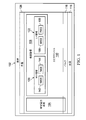
図1を参照すると、装置102は、縦型電力装置104および混合信号表面装置108を含む。
Referring to FIG. 1, the
縦型電力装置104は、バルクシリコン116上のエピタキシャルシリコン110の一部として形成され、金属126および金属118に接続される。縦型電力装置104は、SJMOSFET、IGBT、シリコン接合ダイオード、ショットキーダイオード、または複合装置のような単一の高出力装置を形成する並列に接続された半導体装置を含む。金属126と金属118との間の装置102の高さは、縦型電力装置104の所与のブレークダウン電圧をサポートできるほど十分に高い。縦型電力装置104の最上部は、装置102の最上部のドーピング領域の一部を形成する。縦型電力装置104は、高電圧端子を上面に戻さずに金属118等を介して高電圧端子を裏面に出す裏面接続を有する。裏面端子は、ドレイン(MOS)、コレクタ(IGBT)、またはカソード(ダイオード)などの1次の高電圧通電端子である。裏面端子は、装置の主要機能に関与していない寄生容量や寄生接合のような寄生端子ではない。
表面装置108は、バルクシリコン116上に形成されたエピタキシャルシリコン110内またはその上面に形成された1若しくはそれ以上の複数のアナログ装置およびデジタル装置を含む混合信号装置である。表面装置108は、中電圧(medium voltage:MV)領域120および低電圧(low voltage:LV)領域122を含む。代替的な実施形態は、1若しくはそれ以上のMV領域、1若しくはそれ以上のLV領域、あるいは1若しくはそれ以上のMV領域と1若しくはそれ以上のLV領域との組み合わせを使用する。表面装置108を形成する電子回路は装置102の上面に沿って電気的に活性なので、表面装置108からの電流は底部の金属118または装置102の裏面には流れない。表面装置108は、縦型電力装置104の最上部と共に、装置102の最上部のドーピング領域を形成する。表面装置108を形成する装置は、装置102の上面の横軸に沿って電気的に活性である横型装置であるか、または表面装置領域内に1次の電気的活性が閉じ込められる縦型装置(NPNトランジスタ等)のどちらかである。
The
特定の実施形態では、表面装置108を形成する電子回路は、縦型電力装置104を制御するために使用される。特定の実施形態では、表面装置108は、1若しくはそれ以上の横型NMOS、横型PMOS、LDMOS、縦型NPN、縦型PNP、横型NPN、および横型PNPトランジスタを含む。特定の実施形態では、表面装置108の回路は、1若しくはそれ以上のEPROM(消去可能プログラマブル読み出し専用メモリ)またはEEPROM(電気的に消去可能プログラマブル読み出し専用メモリ)不揮発性メモリ素子を形成する。特定の実施形態では、表面装置108は、1若しくはそれ以上の容量性、誘導性および抵抗性素子を含む。代替的な実施形態は、トランジスタ、抵抗器、コンデンサなどの表面装置108に形成された任意の数またはタイプの電気部品を有することができ、これによりアナログデジタル変換器、デジタルアナログ変換器、論理ゲート、メモリ、プロセッサ、ステートマシン、EPROM、EEPROM、論理ゲートなどの任意の数のデジタルあるいはアナログ部品が形成される。
In certain embodiments, the electronic circuitry forming the
MV領域120は、NMOS領域142およびPMOS領域144の内部に1若しくはそれ以上のトランジスタを有する。追加の実施形態では、NMOS領域142とPMOS領域144との間の特定のトランジスタは、互いに補完して単純な論理ゲートおよびメモリから複雑なステートマシンおよびプロセッサへCMOS論理回路を形成する。
The
LV領域122は、NMOS領域168およびPMOS領域169の内部に1若しくはそれ以上のトランジスタを有する。LV領域122は、MV領域120のトランジスタよりも低電圧でより小さいトランジスタサイズを使用する。
The
金属126は、1若しくはそれ以上の金属の層を含む。縦型電力装置104に電流を流すために、金属の最上層は厚く(厚さ約2〜5マイクロメートル[μm])されている。
表面装置108を接続する金属126の部分のために、金属126は、厚さ約0.3〜1.0μmでシリコンに最も近い、MV領域120およびLV領域122の高密度配線のための1若しくはそれ以上のより薄い下部金属層を含んでもよい。次に、これらのより薄い層には、最上金属層の厚い電力装置金属層がかぶせられる。縦型電力装置104の上にあるより薄い金属の層126はスタックされ、厚い最上金属層からより薄い金属層を通って最終的に縦型電力装置104まで電流を運ぶためのビアを含む。
For the portion of the
バルクシリコン116上のエピタキシャルシリコン110の一部は表面装置108の下に電流を流さないので、エピタキシャルシリコン110のこの部分は、縦型電力装置104を形成するエピタキシャルシリコン110の一部よりも低温である。特定の実施形態では、表面装置108の各領域は、縦型装置領域の周りまたは内部に戦略的に配置または点在して配置され、縦型電力装置104から熱を放熱させ、装置102の全体的な温度を低下させる。
Since a portion of the
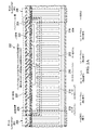
図2Aを参照すると、バルクシリコン上のエピタキシャル内または上にある混合信号装置と組み合わされた縦型電力超接合MOSFET(superjunction MOSFET:SJMOSFET)を有する半導体装置202の断面図が示されている。装置202は、図1の装置102の実施形態である。
Referring to FIG. 2A, a cross-sectional view of a
装置202は、すべてバルクシリコン216上のエピタキシャルシリコン210内または上に形成される第1のSJMOSFET部分204、第2のSJMOSFET部分206、および表面装置208を含む。
第1のSJMOSFET部分204および第2のSJMOSFET部分206は、互いに電気的に接続している。追加のSJMOSFET部分を含めることで、装置202上に形成されたSJMOSFETの電力処理能力を高めてもよい。
The
エピタキシャルシリコン210は、N−型エピタキシャル層214内に形成されたP−型シリコンカラム212を含む。P−型シリコンカラム212およびN−型エピタキシャル層214は、約4〜6×10¹⁵(中E15)cm−3から約1〜3×10¹⁶(低E16)cm−3の濃度にドープされる。N+層216は、ウェハの裏面の金属層218と接触するバルクシリコンの層である。
特定の実施形態では、P−型カラム212は、n+バルク基板上に配置された1若しくはそれ以上のn−型エピタキシャルシリコン堆積のそれぞれに、マスクされたp−型注入を実行することによって構成される。特定の実施形態では、P−型カラム212は、n+バルク基板上に配置されたn−型エピタキシャル領域にトレンチをエッチングし、トレンチ側壁にP−型インプラントを注入し、ドープされていないエピタキシャルシリコンまたはシリコン酸化物(silicon oxide)をトレンチに再充填することによって構成される。特定の実施形態では、P−型カラム212は、n+バルク基板上に配置されたn−型エピタキシャル領域にトレンチをエッチングし、トレンチ内でシリコン酸化物を成長させ、トレンチ側壁にP−型インプラントを注入し、ドープされたまたはドープされていないポリシリコンをトレンチに再充填することによって構成される。
In certain embodiments, the P−
特定の実施形態では、高電圧終端領域は装置202のSJMOSFETに必要とされないが、それは隣接する超接合カラムの電荷バランスを乱さないように十分に低い内部電荷を有するトレンチ絶縁材料に、十分な電気的分離を提供する縦型にエッチングされた絶縁トレンチを追加するためである。特定の実施形態では、縦型にエッチングされた絶縁トレンチは、P−型のカラム幅を実質的に二等分して電荷バランスを維持する。
In certain embodiments, a high voltage termination region is not required for the SJMOSFET of
特定の実施形態では、縦型にエッチングされた絶縁トレンチは、N−型のカラム幅を実質的に二等分して電荷バランスを維持する。バルクシリコン上のエピタキシャル技術を使用する設計では、SOI技術に存在するような縦型にエッチングされた絶縁トレンチが追加され、バルク上のエピタキシャル技術において使用される高電圧終端領域が消費する面積を低減する。縦型にエッチングされた絶縁トレンチは、表面装置の領域を電力装置の各領域から横方向に電気的に絶縁する一方で、バルク上のエピタキシャル設計には底部絶縁体がないので、依然として接合/ドリフト絶縁に依存して縦型の電気的絶縁を提供する。 In certain embodiments, the vertically etched isolation trench substantially bisects the N-type column width to maintain charge balance. Designs using epitaxial technology on bulk silicon add vertical etched isolation trenches as present in SOI technology, reducing the area consumed by high voltage termination regions used in epitaxial technology on bulk To do. Vertically etched isolation trenches electrically isolate the surface device regions laterally from each region of the power device, while the epitaxial design on the bulk does not have a bottom insulator so it is still junction / drift Rely on the insulation to provide vertical electrical insulation.
特定の実施形態では、表面装置208は、中電圧(medium voltage:MV)領域220および低電圧(low voltage:LV)領域222を含む。表面装置208は、例として4つのトランジスタを含む。代替的な実施形態は、ただ1つのMV領域、ただ1つのLV領域、またはその組み合わせを有することができ、トランジスタ、抵抗器、コンデンサなどの任意の数またはタイプの電気部品を有することができるので、これによりアナログデジタル変換器、デジタルアナログ変換器、論理ゲート、メモリ、プロセッサ、ステートマシン、EPROM、EEPROM、論理ゲートなどの任意の数またはタイプのデジタルまたはアナログ部品が形成される。
In certain embodiments, the
パッシベーション層224は装置202の上面を覆って、装置202が環境要因の影響を受けにくいようにする。パッシベーション層224は、酸化物、窒化物、ポリイミドなどの1若しくはそれ以上で形成される。
The
図2Bは、SJMOSFET部分204の断面をより詳細に示す。
FIG. 2B shows the cross section of the
金属226は、SJMOSFET部分204のソースと、SJMOSFET部分206などの他のSJMOSFET部分のソースとを相互接続する。代替的な実施形態では、多層金属トポロジを使用してもよい。多層金属トポロジはすべての層にアルミニウム(Al)を使用してもよく、あるいは、最上層が装置202のSJMOSFETの高電力要件を処理するのに十分に厚い(厚さ約2〜5マイクロメートル[μm])限り、最下層の金属層に対するAlと最上層の金属層に対する銅(Cu)とを組み合わせて使用してもよい。MV領域220およびLV領域222の金属層のために、金属層226は、厚さ約0.3〜1.0μmでシリコンに最も近い、MV領域220およびLV領域222の高密度配線のための1若しくはそれ以上のより薄い下部金属層を有していてもよい。次に、これらのより薄い層には、最上金属層の厚い電力装置金属層がかぶせられる。より薄い金属層を有する装置202のSJMOSFET部分に対して、下部金属層および下部ビア層のスタックは、最上金属層からシリコン内のSJMOSFETに電流を運ぶ。
Metal 226 interconnects the source of
ビア228は、コンタクト底部を有するタングステン(W)プラグと、チタン(Ti)、窒化チタン(TiN)、またはそれらの組み合わせなどのバリア層で裏打ちされた側壁とで作られる。 Via 228 is made of a tungsten (W) plug with a contact bottom and sidewalls lined with a barrier layer such as titanium (Ti), titanium nitride (TiN), or combinations thereof.
層間絶縁膜(Interlayer dielectric:ILD)230は、多結晶シリコンからなるゲート238と金属226との間の誘電体材料の層である。装置202のSJMOSFETのような電力装置は、表面から最も近くに非荷電非ドープ酸化物層(非プラズマ強化堆積)を有する複数のSiO2(酸化物)層を典型的に有し、ドープされた(例えば、PSG(フォスフォシリケートグラス))およびプラズマ堆積酸化物(例えば、PETEOS(プラズマ強化テトラエチルオルトシリケート))が続く。
The interlayer dielectric (ILD) 230 is a dielectric material layer between the
電界酸化物232は電力装置のための層電界酸化物であり、通常(表面に)厚く堆積された酸化物であり(すなわち、シリコンの局所酸化(local oxidation of silicon:LOCOS)ではない)、湿式エッチングされて45°に非常に近い傾斜が与えられてスムーズに変化する電界を維持する。これは、電力装置が(電界がほぼ縦型である)コア領域から(電界が水平および縦型の組み合わせであり、ほぼ水平である)終端領域に遷移する際に重要である。
ゲート酸化物234は、ゲート238をnカラムおよびp−ボディ236から分離する。
P−ボディドーピング236は、VDMOS(縦型拡散金属酸化物半導体)装置とも呼ばれるSJMOSFET部分204のチャネル領域を形成する。P−ボディ236はN+およびP−ベースのドーピング領域を含むが、図示していない。
P-
ゲート238はポリシリコンを有し、ゲート238に印加される電圧は、装置202のSJMOSFETのソースとドレインとの間を通過する電流の量を制御する。
The
図2Cは、表面装置208の断面図である。表面装置208は、中電圧(medium voltage:MV)領域220および低電圧(low voltage:LV)領域222を含む。中電圧領域220および低電圧領域222は、それぞれ2つの例示的MOSFET装置を有する。別の実施形態では、表面装置208は、アナログ信号処理およびデジタル信号処理のうちの1若しくはそれ以上を実行する追加のトランジスタおよび部品を含む。代替的な一実施形態では、表面装置208は、SJMOSFET装置202のオン/オフ状態を制御するために使用されるステートマシンを形成する追加のトランジスタを含む。表面装置208は、エピタキシャルシリコン210の上部に形成された中電圧P−型ウェル(medium voltage P−type well:MV P−ウェル)240を含む。MV P−ウェル240はおよそ低〜中E16cm−3濃度にドープされ、その下限は、MV P−ウェル240のドーピング濃度がN−型エピタキシャル層214のバックグラウンドドーピング濃度よりも高くなるように、N−型エピタキシャル層214の濃度によって制限される。
FIG. 2C is a cross-sectional view of the
図2Dは、装置202の中電圧領域220の断面図である。中電圧領域220は、中電圧N−型金属酸化物半導体(medium voltage N−type metal oxide semiconductor:MV NMOS)領域242および中電圧P−型金属酸化物半導体(medium voltage P−type metal oxide semiconductor:MV PMOS)領域244を含む。
FIG. 2D is a cross-sectional view of the
MV NMOS領域242は、MV P−ウェル240内に形成されたトランジスタ246を含む。
The
MV PMOS領域244は、MV N−ウェル250内に形成されたトランジスタ248を含む。MV N−ウェル250は、MV P−ウェル240の内部に形成され、中E16cm−3濃度にドープされ、その下限は、MV N−ウェル250のドーピング濃度がMV P−ウェル240のバックグラウンドドーピング濃度よりも高くなるように、MV P−ウェル240のドーピング濃度によって制限される。
The
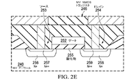
図2Eは、MV NMOS領域242におけるトランジスタ246の断面図である。トランジスタ246は、ゲート252と、ソース254と、ドレイン256とを含む。ゲート252は、ゲート252に印加される電圧に基づいてソース253とドレイン254との間の電流を制御する多結晶シリコンで作られる。ゲート酸化物層255は、ゲート252をエピタキシャルシリコン210から分離する。ソース253は、MV P−ウェル240内のエピタキシャルシリコン210の上部に形成されたN+領域256およびN++領域257を有する。ドレイン254は、MV P−ウェル240内のエピタキシャルシリコン210の上部に形成されたN+領域258およびN++領域259を有する。N++領域257および259のドーズ量は約3〜7E15cm−2で、濃度は約7〜9×10¹⁹(高E19)〜中E20cm−3である。N+領域256および258は、N++領域257および259をそれぞれ囲んで、横方向電界をグレードアウトし、トランジスタ246を中電圧レベルで動作可能にする。N+領域256および258のドーズ量は高E13〜高E14cm−2で、濃度は中E17〜高E18 cm−3である。
FIG. 2E is a cross-sectional view of
図2Fは、MV PMOS領域244におけるトランジスタ248の断面図である。トランジスタ248は、ゲート260と、ソース261と、ドレイン262とを含む。ゲート260は、ゲート260に印加される電圧に基づいてソース261とドレイン262との間の電流を制御する多結晶シリコンで作られる。ゲート酸化物層263は、ゲート260をエピタキシャルシリコン210から分離する。ソース261は、MV N−ウェル250内のエピタキシャルシリコン210の上部に形成されたP+領域264およびP++領域265を有する。ドレイン262は、MV N−ウェル250内のエピタキシャルシリコン210の上部に形成されたP+領域266およびP++領域267を有する。P++領域265および267のドーズ量は約1〜5 E15cm−2で、濃度は中E19〜中E20cm−3である。P+領域264および266は、P++領域265および267をそれぞれ囲んで、横方向電界をグレードアウトし、トランジスタ248を中電圧レベルで動作可能にする。P+領域264および266のドーズ量は高E13〜高E14cm−2で、濃度は中E17〜高E18 cm−3である。
FIG. 2F is a cross-sectional view of transistor 248 in
図2Gは、装置202の低電圧領域222の断面図である。低電圧領域222は、低電圧N−型金属酸化物半導体(low voltage N−type metal oxide semiconductor:LV NMOS)領域268および低電圧P−型金属酸化物半導体(low voltage P−type metal oxide semiconductor:LV PMOS)領域269を含む。
FIG. 2G is a cross-sectional view of the
LV NMOS領域268は、LV P−ウェル272内に形成されたトランジスタ270を含む。LV P−ウェル272は、MV P−ウェル240の内部に形成され、約中E16〜中E17cm−3のドーピング濃度を有する。
The LV NMOS region 268 includes a
LV PMOS領域269は、LV N−ウェル273内に形成されたトランジスタ271を含む。LV N−ウェル273は、MV P−ウェル240の内部に形成され、約高E16〜中E17cm−3のドーピング濃度を有し、その下限は、LV N−ウェル273のドーピング濃度がMV P−ウェル240のバックグラウンドドーピング濃度よりも高くなるように、MV P−ウェル240のドーピング濃度によって制限される。
The LV PMOS region 269 includes a
図2Hは、LV NMOS領域268におけるトランジスタ270の断面図である。トランジスタ270は、ゲート274と、ソース275と、およびドレイン276とを含む。ゲート274は、ゲート274に印加される電圧に基づいてソース275とドレイン276との間の電流を制御する多結晶シリコンで作られる。ゲート酸化物層277は、ゲート274をエピタキシャルシリコン210から分離する。ソース275は、MV P−ウェル240の内部に形成されたLV P−ウェル272内のエピタキシャルシリコン210の上部に形成されたN++領域278を有する。ドレイン276は、LV P−ウェル272内のエピタキシャルシリコン210の上部に形成されたN++領域279を有する。N++領域278および279のドーズ量は約3〜7E15cm−2で、濃度は高E19〜中E20cm−3である。
FIG. 2H is a cross-sectional view of
図2Iは、LV PMOS領域269におけるトランジスタ271の断面図である。トランジスタ271は、ゲート280と、ソース281と、ドレイン282とを含む。ゲート280は、ゲート280に印加される電圧に基づいてソース281とドレイン282との間の電流を制御する多結晶シリコンで作られる。ゲート酸化物層283は、ゲート280をエピタキシャルシリコン210から分離する。ソース281は、LV N−ウェル273内のエピタキシャルシリコン210の上部に形成されたP++領域285を有する。ドレイン282は、LV N−ウェル273内のエピタキシャルシリコン210の上部に形成されたP++領域284を有する。P++領域284および285のドーズ量は約1〜5 E15cm−2で、濃度は中E19〜中E20cm−3である。
FIG. 2I is a cross-sectional view of
図2Jは、SJMOSFET部分204と並列である超接合IGBT(super junction IGBT:SJIGBT)部分207を含む縦型電力装置を有する装置の断面図である。SJIGBTをSJMOSFETと並列で提供することにより、複合超接合IGBTおよびMOSFET高電圧装置が形成される。SJIGBT部分207およびSJMOSFET部分204のゲートバスは、SJIGBT部分207およびSJMOSFET部分204のオンオフタイミングを個別に制御するために分離可能である。SJIGBT部分207およびSJMOSFET部分204の相対的オンオフタイミングを最適化することにより、MOSFETの優れたスイッチング速度とIGBTの優れた電流処理能力とを組み合わせた複合装置が得られる。特定の実施形態では、埋め込み混合信号回路は、SJIGBT部分207およびSJMOSFET部分204の相対的なオンオフタイミングを制御して、複合装置のスイッチング速度および電流処理能力を最適化する。
FIG. 2J is a cross-sectional view of a device having a vertical power device that includes a super junction IGBT (SJIGBT) portion 207 that is in parallel with the
図3Aを参照すると、バルクシリコン上のエピタキシャル内の混合信号装置と組み合わされた縦型IGBTを有する半導体装置302の断面図が示されている。装置302は、図1の装置102の実施形態である。
Referring to FIG. 3A, a cross-sectional view of a
第1のIGBT部分304および第2のIGBT部分306は、互いに電気的に接続している。追加のIGBT部分を含めることで、装置302上に形成されたIGBTの電力処理能力を高めてもよい。
The
エピタキシャルシリコン310はN−型エピタキシャル層314を含み、このN−型エピタキシャル層314は、約4〜6×10¹⁵(中E15)cm−3〜約1〜3×10¹⁶(低E16)cm−3の濃度にドープされる。バルクシリコンN+層316および金属層318は、ウェハの裏面に形成される。
表面装置308は、中電圧(medium voltage:MV)領域320および低電圧(low voltage:LV)領域322を含む。表面装置308は、4つのトランジスタを含む。代替的な実施形態は、ただ1つのMV領域、ただ1つのLV領域、またはその組み合わせを有することができ、トランジスタ、抵抗器、コンデンサなどの任意の数またはタイプの電気部品を有することができるので、これによりアナログデジタル変換器、デジタルアナログ変換器、論理ゲート、メモリ、プロセッサ、ステートマシンなどの任意の数またはタイプのデジタルまたはアナログ部品が形成される。
The
パッシベーション層324は、装置302の上面を覆って、装置302が環境要因の影響を受けにくいようにする。パッシベーション層324は、酸化物、窒化物、ポリイミドなどの1若しくはそれ以上で形成される。
The
図3Bは、IGBT部分304の断面をより詳細に示す。
FIG. 3B shows the cross section of the
金属326は、IGBT部分304のエミッタと、IGBT部分306などの他のIGBT部分のエミッタとを相互接続する。代替的な実施形態では、多層金属トポロジを使用してもよい。多層金属トポロジはすべての層にアルミニウム(Al)を使用してもよく、あるいは、最上層が装置302のIGBTの高電力要件を処理するのに十分に厚い(厚さ約2〜5マイクロメートル[μm])限り、最下層の金属層に対するAlと最上層の金属層に対する銅(Cu)とを組み合わせて使用してもよい。MV領域320のMV NMOSトランジスタ346のソースは、金属326によって装置302のIGBTのエミッタに接続されている。
ビア328は、コンタクト底部を有するタングステン(W)プラグと、チタン(Ti)、窒化チタン(TiN)、またはそれらの組み合わせなどのバリア層で裏打ちされた側壁とで作られる。 Via 328 is made of a tungsten (W) plug with a contact bottom and sidewalls lined with a barrier layer such as titanium (Ti), titanium nitride (TiN), or combinations thereof.
層間絶縁膜(Interlayer dielectric:ILD)330は、多結晶シリコンからなるゲートと金属326との間の誘電体材料の層である。装置302のIGBTのような電力装置は、表面から最も近くに非荷電非ドープ酸化物層(非プラズマ強化堆積)を有する複数のSiO2(酸化物)層を典型的に有し、ドープされた(例えば、PSG)およびプラズマ堆積酸化物(例えば、PETEOS)が続く。
An interlayer dielectric (ILD) 330 is a layer of dielectric material between the gate made of polycrystalline silicon and the
電界酸化物332は電力装置のための層電界酸化物であり、(表面に)厚く堆積された酸化物であり(すなわち、シリコンの局所酸化(local oxidation of silicon:LOCOS)ではない)、湿式エッチングされて45°に非常に近い傾斜が与えられてスムーズに変化する電界を維持する。これは、電力装置が(電界がほぼ縦型である)コア領域から(電界が水平および縦型の組み合わせであり、ほぼ水平である)終端領域に遷移する際に重要である。
ゲート酸化物334は、ウェハのエピタキシャルシリコン310内のN−型エピタキシャル層314からゲート338を分離する。
The
低E16cm−3〜低E18cm−3のドーピング範囲を有するP−ボディドーピング336は、IGBT部分306のエピタキシャルシリコン310の上面に向かって形成される。N++層331は、P−ボディ336内に形成される。
A P-
ゲート338はポリシリコンを有し、ゲート338に印加される電圧は、装置302のIGBTのエミッタとコレクタとの間を通過する電流の量を制御する。図面を分かりやすくするために、ゲート接触および制御は示していない。
P+層339は、N+層316とP−N接合を形成して、第1のIGBT部分304のコレクタを形成する。
P +
図3Cは、表面装置308の断面図である。表面装置308は、中電圧(medium voltage:MV)領域320および低電圧(low voltage:LV)領域322を含む。中電圧領域320および低電圧領域322は、それぞれ2つの例示的MOSFET装置を有する。別の実施形態では、表面装置308は、アナログ信号処理およびデジタル信号処理のうちの1若しくはそれ以上を実行する追加のトランジスタおよび部品を含む。代替的な一実施形態では、表面装置308は、装置302のIGBTのオン/オフ状態を制御するために使用されるステートマシンを形成する追加のトランジスタを含む。表面装置308は、エピタキシャルシリコン310の頂部に形成された中電圧P−型ウェル(medium voltage P−type well:MV P−ウェル)340を含む。MV P−ウェル340はおよそ低〜中E16cm−3濃度にドープされ、その下限は、MV P−ウェル340のドーピング濃度がN−型エピタキシャル層314のバックグラウンドドーピング濃度よりも高くなるように、N−型エピタキシャル層314の濃度によって制限される。
FIG. 3C is a cross-sectional view of the
金属326は、ILD330の頂部に単一の不連続層として形成される。代替的な実施形態では、MV領域320およびLV領域322の金属層のために、金属層326は、厚さ約0.3〜1.0μmでシリコンに最も近い、MV領域320およびLV領域322の高密度配線のための1若しくはそれ以上の「薄い」下部金属層を有していてもよい。次に、これらの薄い層には、最上金属層の厚い電力装置金属層がかぶせられる。薄い金属層を有する装置302のIGBT部分に対して、下部金属層および下部ビア層のスタックは、最上金属層からシリコン内のIGBTに電流を運ぶ。
中電圧領域320は、中電圧N−型金属酸化物半導体(medium voltage N−type metal oxide semiconductor:MV NMOS)領域342および中電圧P−型金属酸化物半導体(medium voltage P−type metal oxide semiconductor:MV PMOS)領域344を含む。MV NMOS領域342は、MV P−ウェル340内に形成されたトランジスタ346を含む。MV PMOS領域344は、MV N−ウェル350内に形成されたトランジスタ348を含む。
The
MV N−ウェル350は、MV P−ウェル340の内部に形成され、中E16cm−3濃度にドープされ、その下限は、MV N−ウェル350のドーピング濃度がMV P−ウェル340のバックグラウンドドーピング濃度よりも高くなるように、MV P−ウェル340のドーピング濃度によって制限される。 The MV N-well 350 is formed inside the MV P-well 340 and is doped to a medium E16 cm −3 concentration, the lower limit being that the doping concentration of the MV N-well 350 is the background doping concentration of the MV P-well 340 Is limited by the doping concentration of the MVP-well 340.
MV NMOS領域342のトランジスタ346およびMV PMOS領域344のトランジスタ348はそれぞれ、図2Eのトランジスタ246および図2Fのトランジスタ248と形態および機能において同様である。
低電圧領域322は、低電圧N−型金属酸化物半導体(low voltage N−type metal oxide semiconductor:LV NMOS)領域368および低電圧P−型金属酸化物半導体(low voltage P−type metal oxide semiconductor:LV PMOS)領域369を含む。LV NMOS領域368は、LV P−ウェル372内に形成されたトランジスタ370を含む。LV P−ウェル372は、MV P−ウェル340の内部に形成され、約中E16〜中E17cm−3のドーピング濃度を有する。
The low voltage region 322 includes a low voltage N-type metal oxide semiconductor (LV NMOS)
LV PMOS領域369は、LV N−ウェル373内に形成されたトランジスタ371を含む。LV N−ウェル373は、MV P−ウェル340の内部に形成され、約高E16〜中E17cm−3のドーピング濃度を有し、その下限は、LV N−ウェル373のドーピング濃度がMV P−ウェル340のバックグラウンドドーピング濃度よりも高くなるように、MV P−ウェル340のドーピング濃度によって制限される。
The
LV NMOS領域368のトランジスタ370およびLV PMOS領域369のトランジスタ371はそれぞれ、図2Hのトランジスタ270および図2Iのトランジスタ271と形態および機能において同様である。
図4Aを参照すると、バルクシリコン上のエピタキシャル内または上にある混合信号装置と組み合わされた縦型電力ダイオードを有する半導体装置402の断面図が示されている。装置402は、図1の装置102の実施形態である。
Referring to FIG. 4A, a cross-sectional view of a
第1のダイオード部分404および第2のダイオード部分406は、互いに電気的に接続している。追加のダイオード部分を含めることで、装置402上に形成されたダイオードの電力処理能力を高めてもよい。
The
エピタキシャルシリコン410は、N−型エピタキシャル層414を含み、このN−型エピタキシャル層414は、約4〜6×10¹⁵(中E15)cm−3から約1〜3×10¹⁶(低E16)cm−3の濃度にドープされる。N+層416は、ウェハの裏面の金属層418と接触するバルクシリコンの層である。
The
表面装置408は、中電圧(medium voltage:MV)領域420および低電圧(low voltage:LV)領域422を含む。表面装置408は、4つのトランジスタを含む。代替的な実施形態は、ただ1つのMV領域、ただ1つのLV領域、またはその組み合わせを有することができ、トランジスタ、抵抗器、コンデンサなどの任意の数またはタイプの電気部品を有することができるので、これによりアナログデジタル変換器、デジタルアナログ変換器、論理ゲート、メモリ、プロセッサ、ステートマシンなどの任意の数またはタイプのデジタルまたはアナログ部品が形成される。
The
パッシベーション層424は、装置402の上面を覆って、装置402が環境要因の影響を受けにくいようにする。パッシベーション層424は、酸化物、窒化物、ポリイミドなどの1若しくはそれ以上で形成される。
The
MV領域420は、MV NMOSトランジスタ446およびMV PMOSトランジスタ448を含む。MV領域420およびそのそれぞれのトランジスタは、図2CのMV領域220および図3CのMV領域320の形態および機能と同様である。
The
LV領域422は、LV NMOSトランジスタ470およびLV PMOSトランジスタ471を含む。LV領域422およびそのそれぞれのトランジスタは、図2CのLV領域222および図3CのLV領域322のトランジスタと形態および機能において同様である。
The LV region 422 includes an
図4Bは、ダイオード部分404の断面をより詳細に示す。
FIG. 4B shows the cross section of the
金属426は、ダイオード部分404のアノードと、ダイオード部分406などの他のダイオード部分のアノードとを相互接続する。代替的な実施形態では、装置402のダイオードの高電力要件を処理するためのアルミニウム(Al)の厚い層を有する多層金属トポロジにおいて、Alまたは銅(Cu)が使用される。多層金属トポロジでは、全面的にAlが使用されるか、あるいはシリコンの近くでAlが使用され、上層でCuが使用される。装置402に電流を流すために、金属の最上層は厚く(厚さ約2〜5マイクロメートル(μm))されている。MV領域420のMV NMOSトランジスタ446のソースは、金属426によって装置402のダイオードのエミッタに接続されている。
ビア428は、コンタクト底部を有するタングステン(W)プラグと、チタン(Ti)、窒化チタン(TiN)、またはそれらの組み合わせなどのバリア層で裏打ちされた側壁とで作られる。 Via 428 is made of a tungsten (W) plug with a contact bottom and sidewalls lined with a barrier layer such as titanium (Ti), titanium nitride (TiN), or combinations thereof.
層間絶縁膜(Interlayer dielectric:ILD)430は、金属426を装置402の電気的に活性な部分から分離する誘電体材料の層である。装置402のダイオードのような電力装置は、表面に最も近くに非荷電非ドープ酸化物層(非プラズマ強化堆積)を有する複数のSiO2(酸化物)層を典型的に有し、ドープされた(例えば、PSG)およびプラズマ堆積酸化物(例えば、PETEOS)が続く。
Interlayer dielectric (ILD) 430 is a layer of dielectric material that separates
電界酸化物432は電力装置のための層電界酸化物であり、(表面に)厚く堆積された酸化物であり(すなわち、シリコンの局所酸化(local oxidation of silicon:LOCOS)ではない)、湿式エッチングされて45°に非常に近い傾斜が与えられてスムーズに変化する電界を維持する。これは、電力装置が(電界がほぼ縦型である)コア領域から(電界が水平および縦型の組み合わせであり、ほぼ水平である)終端領域に遷移する際に重要である。
高E18cm−3から低E20cm−3の範囲でドーピングされたP+層433は、ダイオード部分404のエピタキシャルシリコン410の上面に向かって形成され、ビア428によって金属426に接続される。インターフェース435は、P+層433とN−ドープされたエピタキシャル層414との間のインターフェースであり、P−N接合を形成してシリコン接合ダイオードを作る。インターフェース437は、ビア429とN−ドープされたN−型エピタキシャル層414との間のインターフェースであり、金属−半導体接合を形成してショットキーダイオード用のショットキー障壁を作る。追加の実施形態では、装置402のダイオードは、シリコン接合ダイオードのみを有し、ショットキーダイオードのみを有し、またはシリコン接合ダイオードおよびショットキーダイオードの任意の組み合わせを有する。
A P +
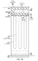
図5は、シリコン・オン・インシュレータ(silicon−on−insulator:SOI)技術を使用して形成された縦型電力装置504および混合信号表面装置508を含む半導体装置502のブロック図である。一実施形態では、縦型電力装置504は表面装置508によって制御される。縦型電力装置504および表面装置508は、エピタキシャルシリコン510上に形成され、絶縁体586によって分離される。
FIG. 5 is a block diagram of a
縦型電力装置504は1若しくはそれ以上の電力装置を有し、そのサブセットは互いに並列に接続されてSJMOSFET、IGBT、シリコン接合ダイオード、ショットキーダイオードなどのような1若しくはそれ以上の電力装置を形成する。縦型電力装置504は金属526と金属518との間に接続され、金属はそれぞれ1若しくはそれ以上の金属の層を含んでいてもよい。電力は、ウェハの上面または前側にある金属526と、ウェハの底面または裏側にある金属518との間で、縦型電力装置504を通って流れる。
The
表面装置508は、アナログ回路およびデジタル回路のうちの1若しくはそれ以上を有する混合信号装置である。表面装置508は、MV NMOS領域542、MV PMOS領域544、LV NMOS領域568、およびLV PMOS領域569などの1若しくはそれ以上のMOS領域を含む。各領域は、1若しくはそれ以上のトランジスタを有する1若しくはそれ以上の回路を有し、種々の回路は金属526によって相互接続される。代替的な実施形態は、トランジスタ、抵抗器、コンデンサなどの表面装置508に形成された任意の数またはタイプの電気部品を有することができ、これによりアナログデジタル変換器、デジタルアナログ変換器、論理ゲート、メモリ、プロセッサ、ステートマシン、EPROM、EEPROM、論理ゲートなどの任意の数のデジタルあるいはアナログ部品が形成される。
The
MV NMOS領域542およびMV PMOS領域544は中電圧レベルで動作し、LV NMOS領域568およびLV PMOS領域569は低電圧レベルで動作する。各領域は、選択的に、絶縁体586によって互いに分離される。
エピタキシャルシリコン510の一部は表面装置508の下に電流を流さないので、エピタキシャルシリコン510のこの部分は、縦型電力装置504を形成するエピタキシャルシリコン510よりも低温である。特定の実施形態では、表面装置508の各領域は、縦型装置領域の周りまたは内部に戦略的に配置または点在して配置され、それにより、縦型電力装置504から熱を放熱させ、装置502の全体的な温度を低下させる。
Because a portion of epitaxial silicon 510 does not pass current under
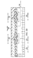
図6Aは、バルクシリコン616上のエピタキシャルシリコン610上に形成され、絶縁体686によって分離される縦型SJMOSFETおよび表面装置608を有する装置602の断面図である。装置602は、図5の装置502の実施形態である。ハンドルウェハ690は、取り扱いおよび処理中に装置602を支持する。第1のSJMOSFET部分604は、エピタキシャルシリコン610内に形成されたP−型カラム612を含む。表面装置608は、絶縁体686によってそれぞれ分離された、MV NMOS領域642、MV PMOS領域644、LV NMOS領域668、およびLV PMOS領域669を有する。MV NMOS領域642、MV PMOS領域644、LV NMOS領域668、およびLV PMOS領域669は、エピタキシャルシリコン610内にP−型カラムを含まない。MV NMOS領域642、MV PMOS領域644、LV NMOS領域668、およびLV PMOS領域669はそれぞれ、それぞれの領域で具体化される装置のタイプに必要な半導体ドーピングタイプおよび濃度を有する単一のウェルを含む。
FIG. 6A is a cross-sectional view of a
図6Bは、第1のSJMOSFET部分604の断面図である。第1のSJMOSFET部分604は、パッシベーション層624、金属626、ILD630、ゲート638、P−ボディドーピング636、ゲート酸化物634、P−型カラム612、N−型エピタキシャル層614、N+層616、金属618を含み、絶縁体686によって囲まれている。第1のSJMOSFET部分604の形態および機能は、図2Aおよび2Bの第1のSJMOSFET部分204の形態および機能と同様である。絶縁体686は、装置602の一部である他の回路から第1のSJMOSFET部分604を分離して絶縁する。
FIG. 6B is a cross-sectional view of the
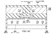
図6Cは、MV NMOS領域642の断面図である。MV NMOS領域642は、エピタキシャルシリコン610内のウェハの上面に形成される。MV NMOS領域642は、絶縁体686によって囲まれ、MV NMOS領域642の上および内部に形成された電気回路を絶縁する。MV NMOS領域642は中電圧レベルを使用し、トランジスタ646を含む。MV P−ウェル640は、他の半導体ドーピングタイプおよび濃度のウェルを含まない。MV P−ウェル640の代替的な実施形態は、他の半導体ドーピングタイプおよび濃度のウェルを含み得る。
FIG. 6C is a cross-sectional view of the
トランジスタ646は、エピタキシャルシリコン610内に形成されたMV NMOS領域642から酸化物655によって分離されたゲート652を含む。トランジスタ646は、N++層657およびN+層656によって形成されたソース653を含む。トランジスタ646は、N++層659およびN+層658によって形成されたドレイン654を含む。
Transistor 646 includes a gate 652 separated by an
図6Dは、MV PMOS領域644の断面図である。MV PMOS領域644は、エピタキシャルシリコン610内のウェハの上面に形成される。MV PMOS領域644は、絶縁体686によって囲まれ、MV PMOS領域644の上および内部に形成された電気回路を絶縁する。MV PMOS領域644は中電圧レベルを使用し、トランジスタ648を含む。MV N−ウェル650は、他の半導体ドーピングタイプおよび濃度のウェルを含まない。MV N−ウェル650の代替的な実施形態は、MV N−ウェル650内に形成された他の半導体ドーピングタイプおよび濃度のウェルを使用する。
FIG. 6D is a cross-sectional view of the
トランジスタ648は、エピタキシャルシリコン610内に形成されたMV PMOS領域644から酸化物663によって分離されたゲート660を含む。トランジスタ648は、P++層665およびP+層664によって形成されたソース661を含む。トランジスタ648は、P++層665およびP+層664によって形成されたドレイン662を含む。
トランジスタ646のドレイン654およびトランジスタ648のドレイン662は、金属626によって接続されている。一実施形態では、トランジスタ646のゲート652およびトランジスタ648のゲート660は電気的に接続されてCMOSインバータの入力を形成し、トランジスタ646のドレイン654およびトランジスタ648のドレイン662はCMOSインバータの出力を形成する。
The
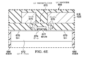
図6Eは、LV NMOS領域668の断面図である。LV NMOS領域668は、エピタキシャルシリコン610内のウェハの上面に形成される。LV NMOS領域668は、絶縁体686によって囲まれ、LV NMOS領域668の上および内部に形成された電気回路を絶縁する。LV NMOS領域668は低電圧レベルを使用し、トランジスタ670を含む。LV P−ウェル672は、他の半導体ドーピングタイプおよび濃度のウェルを含まない。LV P−ウェル672の代替的な実施形態は、他の半導体ドーピングタイプおよび濃度のウェルを含み得る。
FIG. 6E is a cross-sectional view of the
トランジスタ670は、エピタキシャルシリコン610内に形成されたLV NMOS領域668から酸化物677によって分離されたゲート674を含む。トランジスタ670は、N++層678によって形成されたソース675を含む。トランジスタ670は、N++層679によって形成されたドレイン676を含む。
Transistor 670 includes a
図6Fは、LV PMOS領域669の断面図である。LV PMOS領域669は、エピタキシャルシリコン610内のウェハの上面に形成される。LV PMOS領域669は、絶縁体686によって囲まれ、LV PMOS領域669の上および内部に形成された電気回路を絶縁する。LV PMOS領域669は低電圧レベルを使用し、トランジスタ671を含む。LV N−ウェル673は、他の半導体ドーピングタイプおよび濃度のウェルを含まない。LV N−ウェル670の代替的な実施形態は、LV N−ウェル670内に形成された他の半導体ドーピングタイプおよび濃度のウェルを使用する。
FIG. 6F is a cross-sectional view of the
トランジスタ671は、エピタキシャルシリコン610内に形成されたLV PMOS領域669から酸化物683によって分離されたゲート680を含む。トランジスタ671は、P++層685によって形成されたソース681を含む。トランジスタ671は、P++層684によって形成されたドレイン682を含む。明確にするために、中間金属層およびゲートへのコンタクトは示していない。
トランジスタ670のドレイン676およびトランジスタ671のドレイン682は、金属626によって接続されている。一実施形態では、トランジスタ670のゲート674およびトランジスタ671のゲート680は電気的に接続されてCMOSインバータの入力を形成し、トランジスタ670のドレイン676およびトランジスタ671のドレイン682はCMOSインバータの出力を形成する。
The
図7Aは、第1のIGBT部分704および表面装置708を含む装置702の断面図である。装置702は図5の装置502の実施形態であり、図6Aの装置602と異なる点は、図7Aの実施形態における縦型電力装置が縦型電力IGBTであるのに対し、図6Aの実施形態における縦型電力装置は縦型電力SJMOSFETであるという点である。ハンドルウェハ790は、取り扱いおよび処理中に装置702を支持する。
FIG. 7A is a cross-sectional view of a
表面装置708は、図6Aの表面装置608と形態および機能において同様であり、MV NMOS領域742、MV PMOS領域744、LV NMOS領域768、およびLV PMOS領域769を含む。MV NMOS領域742、MV PMOS領域744、LV NMOS領域768、およびLV PMOS領域769の各々は、絶縁体786によって囲まれている。MV NMOS領域742、MV PMOS領域744、LV NMOS領域768、およびLV PMOS領域769の各々は、エピタキシャルシリコン710の頂部に形成されたトランジスタを有する。代替的な実施形態では、それぞれが任意の数の電気部品を含む任意の数のMOS領域が組み合わされて、1つ若しくは以上の縦型電力装置を制御するために使用され得る表面装置708を形成する。
図7Bは、装置702の縦型IGBTの断面図である。装置702の縦型IGBTは、ゲート738を含むトレンチゲートIGBTである。明確にするために、中間金属層およびゲートへのコンタクトは示していない。
FIG. 7B is a cross-sectional view of the vertical IGBT of the
金属726は、IGBT部分704のエミッタと、表面装置708を含む他の電子回路とを相互接続する。代替的な実施形態では、多層金属トポロジを使用してもよい。多層金属トポロジはすべての層にアルミニウム(Al)を使用してもよく、あるいは、最上層が装置702のIGBTの高電力要件を処理するのに十分に厚い(厚さ約2〜5マイクロメートル[μm])限り、最下層の金属層に対するAlと最上層の金属層に対する銅(Cu)とを組み合わせて使用してもよい。MV NMOS領域742のトランジスタのソースは、金属726によって装置702のIGBTのエミッタに接続されている。
ビア728は、コンタクト底部を有するタングステン(W)プラグと、チタン(Ti)、窒化チタン(TiN)、またはそれらの組み合わせなどのバリア層で裏打ちされた側壁とで作られる。 Via 728 is made of a tungsten (W) plug with a contact bottom and sidewalls lined with a barrier layer such as titanium (Ti), titanium nitride (TiN), or combinations thereof.
ILD730は、エピタキシャルシリコン710の頂部と金属726との間の誘電体材料の層である。装置702のIGBTのような電力装置は、表面から最も近くに非荷電非ドープ酸化物層(非プラズマ強化堆積)を有する複数のSiO2(酸化物)層を典型的に有し、ドープされた(例えば、PSG)およびプラズマ堆積酸化物(例えば、PETEOS)が続く。
The
ゲート酸化物734は、ウェハのエピタキシャルシリコン710内のN−型エピタキシャル層714からゲート738を分離する。
The
P−ボディドーピング736は、IGBT部分704のエピタキシャルシリコン710の上面に向かって形成される。N++層731は、P−ボディ736内に形成される。
P-
ゲート738はポリシリコンを有し、ゲート738に印加される電圧は、装置702のIGBTのエミッタとコレクタとの間を通過する電流の量を制御する。図面を分かりやすくするために、ゲート接触および制御は示していない。
P+層739は、N+層316とP−N接合を形成して、第1のIGBT部分704のコレクタを形成する。
The P +
図8Aは、第1のダイオード部分804および表面装置808を含む装置802の断面図である。装置802は、図5の装置502の実施形態であり、図6Aの装置602と異なる点は、図8Aの実施形態における縦型電力装置が縦型電力ダイオードであるのに対し、図6Aの実施形態における縦型電力装置は縦型電力SJMOSFETであるという点である。装置802は、ハンドルウェハなしで示している。
FIG. 8A is a cross-sectional view of a
表面装置808は、図6Aの表面装置608と形態および機能において同様であり、MV NMOS領域842、MV PMOS領域844、LV NMOS領域868、およびLV PMOS領域869を含む。MV NMOS領域842、MV PMOS領域844、LV NMOS領域868、およびLV PMOS領域869の各々は、絶縁体886によって囲まれている。MV NMOS領域842、MV PMOS領域844、LV NMOS領域868、およびLV PMOS領域869の各々は、エピタキシャルシリコン810の頂部に形成されたトランジスタを有する。代替的な実施形態では、それぞれが任意の数の電気部品を含む任意の数のMOS領域が組み合わされて、1つ若しくは以上の縦型電力装置を制御するために使用され得る表面装置808を形成する。
図8Bは、ダイオード部分804の断面をより詳細に示す。 FIG. 8B shows a cross section of the diode portion 804 in more detail.
金属826は、ダイオード部分804のアノードと表面装置802とを相互接続する。代替的な実施形態では、金属826は、ダイオード部分804のアノードと、他のダイオード部分のアノードとを相互接続する。他の代替的な実施形態では、多層金属トポロジを使用してもよい。多層金属トポロジはすべての層にアルミニウム(Al)を使用してもよく、あるいは、最上層が装置802のダイオードの高電力要件を処理するのに十分に厚い(厚さ約2〜5マイクロメートル[μm])限り、最下層の金属層に対するAlと最上層の金属層に対する銅(Cu)とを組み合わせて使用してもよい。
Metal 826 interconnects the anode of diode portion 804 and
ビア828は、コンタクト底部を有するタングステン(W)プラグと、チタン(Ti)、窒化チタン(TiN)、またはそれらの組み合わせなどのバリア層で裏打ちされた側壁とで作られる。 Via 828 is made of a tungsten (W) plug with a contact bottom and sidewalls lined with a barrier layer such as titanium (Ti), titanium nitride (TiN), or combinations thereof.
ILD830は、金属826を装置802の電気的に活性な部分から分離する誘電体材料の層である。装置802のダイオードのような電力装置は、表面に最も近くに非荷電非ドープ酸化物層(非プラズマ強化堆積)を有する複数のSiO2(酸化物)層を典型的に有し、ドープされた(例えば、PSG)およびプラズマ堆積酸化物(例えば、PETEOS)が続く。
The ILD 830 is a layer of dielectric material that separates the metal 826 from the electrically active portion of the
P+層833は、ダイオード部分804のエピタキシャルシリコン810の上面に向かって形成され、ビア828によって金属826に接続される。インターフェース835は、P+層833とN−ドープされたエピタキシャル層814との間のインターフェースであり、P−N接合を形成してシリコン接合ダイオードを作る。インターフェース837は、ビア829とN−ドープされたN−型エピタキシャル層414との間のインターフェースであり、金属−半導体接合を形成してショットキーダイオード用のショットキー障壁を作る。追加の実施形態では、装置802のダイオードは、シリコン接合ダイオードのみを有し、ショットキーダイオードのみを有し、またはシリコン接合ダイオードおよびショットキーダイオードの任意の組み合わせを有する。
P +
図9は、混合信号表面装置を有する縦型電力装置を有する装置902の3次元図である。装置902は、図5の装置502の実施形態である。
FIG. 9 is a three-dimensional view of a
SJMOSFET904は、P−型カラム912を有するエピタキシャルシリコン910内に形成される。SJMOSFET904の形態および機能は、図2Aおよび図2Bに記載したSJMOSFETのものと同様である。SJMOSFET904のゲートは並列に接続されたいくつかのゲートを含み、その一部は切り詰められてMV領域920のための空間を作る。SJMOSFET904のドレインは、金属層918に接続されたN+層916によって底部または裏側に形成される。
表面装置908は、MV NMOSトランジスタ946およびMV PMOSトランジスタ948から形成されるCMOSインバータを有するMV領域920を含む。トランジスタ946のゲート952およびトランジスタ948のゲート960は、並列に接続されてCMOSインバータへの入力を形成する。トランジスタ946のドレイン954およびトランジスタ948のドレイン962は、互いに接続されてCMOSインバータの出力を形成する。トランジスタ946のソース953は、SJMOSFET904の並列に接続されたソースに接続されている。トランジスタ948のソース961は、電圧VDDに接続されている。
Surface device 908 includes an MV region 920 having a CMOS inverter formed from
MV NMOSトランジスタ946は、MV P−ウェル940の内部に形成される。MV PMOSトランジスタ948は、MV P−ウェル940に形成されたMV N−ウェル950の内部に形成される。
The
本開示に提示される実施形態は、本発明の実現可能な実施例を提供することを意図しているが、本発明を限定することを意図するものではない。例えば、シリコン以外の他の材料をベース半導体材料として使用できる。当業者によって認識されるように、P−型バルクシリコンまたはエピタキシャル層(N−型ではない)を使用し、ドーパントタイプを反転させて相補型装置を形成するのと同様に、必要に応じてN−型およびP−型領域の様々な範囲のドーピングレベルを使用できる。種々のタイプおよび厚さの酸化物材料を使用できる。プレーナゲートおよびトレンチゲートの両方を含む高電圧装置のための種々のタイプのゲート構造を採用できる。任意の一実施形態の任意の特徴、要素、または利点は、他の実施形態の特徴、要素および利点と組み合わせることができる。 The embodiments presented in this disclosure are intended to provide feasible examples of the present invention, but are not intended to limit the present invention. For example, materials other than silicon can be used as the base semiconductor material. As will be appreciated by those skilled in the art, P-type bulk silicon or epitaxial layers (not N-type) are used, and N may be optionally formed as well as inversion of dopant types to form complementary devices. Various ranges of doping levels in the -type and P-type regions can be used. Various types and thicknesses of oxide materials can be used. Various types of gate structures for high voltage devices including both planar gates and trench gates can be employed. Any feature, element, or advantage of any one embodiment can be combined with the features, elements, and advantages of any other embodiment.
Claims (21)
前記半導体装置の縦軸に沿って電気的に活性であり、前記半導体装置の裏面に少なくとも1つの1次電気端子を有する縦型電力装置と、
前記半導体装置の上面に沿って電気的に活性である1若しくはそれ以上の横型装置を有する表面装置と
を有する半導体装置。 A semiconductor device,
A vertical power device that is electrically active along the longitudinal axis of the semiconductor device and has at least one primary electrical terminal on the back surface of the semiconductor device;
A surface device having one or more lateral devices that are electrically active along an upper surface of the semiconductor device.
前記縦型電力装置は、超接合金属酸化物半導体電界効果トランジスタ(SJMOSFET)を形成するものである半導体装置。 The semiconductor device according to claim 1,
The vertical power device is a semiconductor device that forms a superjunction metal oxide semiconductor field effect transistor (SJMOSFET).
前記縦型電力装置は、超接合金属酸化物半導体電界効果トランジスタ(SJMOSFET)と絶縁ゲートバイポーラトランジスタ(IGBT)とを有するものである半導体装置。 The semiconductor device according to claim 1,
The vertical power device includes a super junction metal oxide semiconductor field effect transistor (SJMOSFET) and an insulated gate bipolar transistor (IGBT).
前記縦型電力装置は、超接合金属酸化物半導体電界効果トランジスタ(SJMOSFET)と、絶縁ゲートバイポーラトランジスタ(IGBT)と、電力ダイオードとを有するものである半導体装置。 The semiconductor device according to claim 1,
The vertical power device is a semiconductor device having a super junction metal oxide semiconductor field effect transistor (SJMOSFET), an insulated gate bipolar transistor (IGBT), and a power diode.
前記1若しくはそれ以上の横型装置は、N−型MOS(NMOS)トランジスタ、P−型MOS(PMOS)トランジスタ、横方向拡散MOS(LDMOS)トランジスタ、NPNバイポーラ接合トランジスタ(NPN)、PNPバイポーラ接合トランジスタ(PNP)、フローティングゲートMOSトランジスタ、ダイオード、抵抗器、コンデンサ、インダクタ、および可溶体のうちの1若しくはそれ以上を含み、
前記表面装置は、前記縦型電力装置を制御するように構成されるものである半導体装置。 The semiconductor device according to claim 2,
The one or more lateral devices include N-type MOS (NMOS) transistors, P-type MOS (PMOS) transistors, lateral diffusion MOS (LDMOS) transistors, NPN bipolar junction transistors (NPN), PNP bipolar junction transistors ( PNP), floating gate MOS transistor, diode, resistor, capacitor, inductor, and one or more of fusible bodies,
The surface device is a semiconductor device configured to control the vertical power device.
前記1若しくはそれ以上の横型装置は、消去可能プログラマブル読み出し専用メモリ(EPROM)、電気的消去可能プログラマブル読み出し専用メモリ(EEPROM)、ステートマシン、アナログデジタル変換器、デジタルアナログ変換器、ゲートドライバ、温度センサ、論理ゲート、プロセッサ、および任意の他の混合アナログデジタル回路構造物のうちの1若しくはそれ以上を形成するように相互接続され、
前記表面装置は、前記縦型電力装置を制御するように構成されるものである半導体装置。 The semiconductor device according to claim 2,
The one or more horizontal devices include an erasable programmable read only memory (EPROM), an electrically erasable programmable read only memory (EEPROM), a state machine, an analog to digital converter, a digital to analog converter, a gate driver, and a temperature sensor. Interconnected to form one or more of logic gates, processors, and any other mixed analog digital circuit structures;
The surface device is a semiconductor device configured to control the vertical power device.
前記表面装置は、中電圧領域と低電圧領域とを有し、
前記中電圧領域は、NMOS領域とPMOS領域とを有し、
前記低電圧領域は、NMOS領域とPMOS領域とを有するものである半導体装置。 The semiconductor device according to claim 5.
The surface device has a medium voltage region and a low voltage region,
The medium voltage region has an NMOS region and a PMOS region,
The low-voltage region is a semiconductor device having an NMOS region and a PMOS region.
前記半導体装置の上部に金属層を有するものであり、
前記金属層は、前記縦型電力装置と前記表面装置とを相互接続するものである半導体装置。 The semiconductor device according to claim 1, further comprising:
The semiconductor device has a metal layer on top,
The metal layer is a semiconductor device that interconnects the vertical power device and the surface device.
前記表面装置の一部は前記縦型電力装置の一部に点在して配置され、それにより、前記縦型電力装置からの熱が放熱され、前記半導体装置の全体的な温度が低下するものである半導体装置。 The semiconductor device according to claim 1,
A part of the surface device is scattered and arranged in a part of the vertical power device, whereby heat from the vertical power device is dissipated and the overall temperature of the semiconductor device is lowered. A semiconductor device.
前記縦型電力装置を前記表面装置から分離する絶縁体を有するものであり、
前記半導体装置はシリコン・オン・インシュレータ装置として形成され、前記絶縁体はシリコン酸化物およびアルミニウム酸化物のうちの1つである半導体装置。 The semiconductor device according to claim 8, further comprising an insulator that separates the vertical power device from the surface device,
The semiconductor device is formed as a silicon-on-insulator device, and the insulator is one of silicon oxide and aluminum oxide.
前記半導体装置の縦軸に沿って電気的に活性であり、前記半導体装置の裏面にコレクタ端子を有する絶縁ゲートバイポーラトランジスタ(IGBT)を形成する縦型電力装置と、
前記半導体装置の上面に沿って電気的に活性である1若しくはそれ以上の横型装置を有する表面装置と
を有する半導体装置。 A semiconductor device,
A vertical power device that forms an insulated gate bipolar transistor (IGBT) that is electrically active along the longitudinal axis of the semiconductor device and has a collector terminal on the back surface of the semiconductor device;
A surface device having one or more lateral devices that are electrically active along an upper surface of the semiconductor device.
前記1若しくはそれ以上の横型装置は、N−型MOS(NMOS)トランジスタ、P−型MOS(PMOS)トランジスタ、横方向拡散MOS(LDMOS)トランジスタ、NPNバイポーラ接合トランジスタ(NPN)、PNPバイポーラ接合トランジスタ(PNP)、フローティングゲートMOSトランジスタ、ダイオード、抵抗器、コンデンサ、インダクタ、および可溶体のうちの1若しくはそれ以上を含み、
前記表面装置は、前記縦型電力装置を制御するように構成されるものである半導体装置。 The semiconductor device according to claim 11.
The one or more lateral devices include N-type MOS (NMOS) transistors, P-type MOS (PMOS) transistors, lateral diffusion MOS (LDMOS) transistors, NPN bipolar junction transistors (NPN), PNP bipolar junction transistors ( PNP), floating gate MOS transistor, diode, resistor, capacitor, inductor, and one or more of fusible bodies,
The surface device is a semiconductor device configured to control the vertical power device.
前記1若しくはそれ以上の横型装置は、消去可能プログラマブル読み出し専用メモリ(EPROM)、電気的消去可能プログラマブル読み出し専用メモリ(EEPROM)、ステートマシン、アナログデジタル変換器、デジタルアナログ変換器、ゲートドライバ、温度センサ、論理ゲート、プロセッサ、および任意の他の混合アナログデジタル回路構造物のうちの1若しくはそれ以上を形成するように相互接続され、
前記表面装置は、前記縦型電力装置を制御するように構成されるものである半導体装置。 The semiconductor device according to claim 11.
The one or more horizontal devices include an erasable programmable read only memory (EPROM), an electrically erasable programmable read only memory (EEPROM), a state machine, an analog to digital converter, a digital to analog converter, a gate driver, and a temperature sensor. Interconnected to form one or more of logic gates, processors, and any other mixed analog digital circuit structures;
The surface device is a semiconductor device configured to control the vertical power device.
前記表面装置は、中電圧領域と低電圧領域とを有し、
前記中電圧領域は、NMOS領域とPMOS領域とを有し、
前記低電圧領域は、NMOS領域とPMOS領域とを有するものである半導体装置。 The semiconductor device according to claim 11.
The surface device has a medium voltage region and a low voltage region,
The medium voltage region has an NMOS region and a PMOS region,
The low-voltage region is a semiconductor device having an NMOS region and a PMOS region.
前記半導体装置の上部に金属層を有するものであり、
前記金属層は、前記縦型電力装置と前記表面装置とを相互接続するものである半導体装置。 12. The semiconductor device according to claim 11, further comprising:
The semiconductor device has a metal layer on top,
The metal layer is a semiconductor device that interconnects the vertical power device and the surface device.
前記表面装置の一部は前記縦型電力装置の一部に点在して配置され、それにより、前記縦型電力装置からの熱が放熱され、前記半導体装置の全体的な温度が低下するものである半導体装置。 The semiconductor device according to claim 11.
A part of the surface device is scattered and arranged in a part of the vertical power device, whereby heat from the vertical power device is dissipated and the overall temperature of the semiconductor device is lowered. A semiconductor device.
前記縦型電力装置を前記表面装置から分離する絶縁体を有するものであり、
前記半導体装置はシリコン・オン・インシュレータ装置として形成され、前記絶縁体はシリコン酸化物およびアルミニウム酸化物のうちの1つである半導体装置。 The semiconductor device according to claim 11, further comprising an insulator separating the vertical power device from the surface device,
The semiconductor device is formed as a silicon-on-insulator device, and the insulator is one of silicon oxide and aluminum oxide.
前記半導体装置の縦軸に沿って電気的に活性であり、前記半導体装置の裏面にカソード端子を有するダイオードを形成する縦型電力装置と、
前記半導体装置の上面に沿って電気的に活性である1若しくはそれ以上の横型装置を有する表面装置とを有する半導体装置。 A semiconductor device,
A vertical power device that is electrically active along the longitudinal axis of the semiconductor device and forms a diode having a cathode terminal on the back surface of the semiconductor device;
A surface device having one or more lateral devices that are electrically active along an upper surface of the semiconductor device.
前記1若しくはそれ以上の横型装置は、N−型MOS(NMOS)トランジスタ、P−型MOS(PMOS)トランジスタ、横方向拡散MOS(LDMOS)トランジスタ、NPNバイポーラ接合トランジスタ(NPN)、PNPバイポーラ接合トランジスタ(PNP)、フローティングゲートMOSトランジスタ、ダイオード、抵抗器、コンデンサ、インダクタ、および可溶体のうちの1若しくはそれ以上を含み、
前記1若しくはそれ以上の横型装置は、消去可能プログラマブル読み出し専用メモリ(EPROM)、電気的消去可能プログラマブル読み出し専用メモリ(EEPROM)、ステートマシン、アナログデジタル変換器、デジタルアナログ変換器、ゲートドライバ、温度センサ、論理ゲート、プロセッサ、および任意の他の混合アナログデジタル回路構造物のうちの1若しくはそれ以上を形成するように相互接続され、
前記表面装置は、前記縦型電力装置を制御するように構成されるものである半導体装置。 The semiconductor device according to claim 18.
The one or more lateral devices include N-type MOS (NMOS) transistors, P-type MOS (PMOS) transistors, lateral diffusion MOS (LDMOS) transistors, NPN bipolar junction transistors (NPN), PNP bipolar junction transistors ( PNP), floating gate MOS transistor, diode, resistor, capacitor, inductor, and one or more of fusible bodies,
The one or more horizontal devices include an erasable programmable read only memory (EPROM), an electrically erasable programmable read only memory (EEPROM), a state machine, an analog to digital converter, a digital to analog converter, a gate driver, and a temperature sensor. Interconnected to form one or more of logic gates, processors, and any other mixed analog digital circuit structures;
The surface device is a semiconductor device configured to control the vertical power device.
前記表面装置は、中電圧領域と低電圧領域とを有し、
前記中電圧領域は、NMOS領域とPMOS領域とを有し、
前記低電圧領域は、NMOS領域とPMOS領域とを有するものである半導体装置。 The semiconductor device according to claim 18.
The surface device has a medium voltage region and a low voltage region,
The medium voltage region has an NMOS region and a PMOS region,
The low-voltage region is a semiconductor device having an NMOS region and a PMOS region.
前記縦型電力装置を前記表面装置から分離する絶縁体を有するものであり、
前記半導体装置はシリコン・オン・インシュレータ装置として形成され、前記絶縁体はシリコン酸化物およびアルミニウム酸化物のうちの1つである半導体装置。 The semiconductor device according to claim 18, further comprising an insulator that separates the vertical power device from the surface device,
The semiconductor device is formed as a silicon-on-insulator device, and the insulator is one of silicon oxide and aluminum oxide.
Applications Claiming Priority (3)
| Application Number | Priority Date | Filing Date | Title |
|---|---|---|---|
| US201562126240P | 2015-02-27 | 2015-02-27 | |
| US62/126,240 | 2015-02-27 | ||
| PCT/US2016/019917 WO2016138468A1 (en) | 2015-02-27 | 2016-02-26 | Surface devices within a vertical power device |
Publications (2)
| Publication Number | Publication Date |
|---|---|
| JP2018511168A true JP2018511168A (en) | 2018-04-19 |
| JP2018511168A5 JP2018511168A5 (en) | 2019-04-25 |
Family
ID=56789964
Family Applications (1)
| Application Number | Title | Priority Date | Filing Date |
|---|---|---|---|
| JP2017545244A Pending JP2018511168A (en) | 2015-02-27 | 2016-02-26 | Surface device in vertical power unit |
Country Status (6)
| Country | Link |
|---|---|
| US (2) | US9755058B2 (en) |
| EP (1) | EP3262678A4 (en) |
| JP (1) | JP2018511168A (en) |
| KR (1) | KR20170121224A (en) |
| CN (1) | CN107851614A (en) |
| WO (1) | WO2016138468A1 (en) |
Families Citing this family (5)
| Publication number | Priority date | Publication date | Assignee | Title |
|---|---|---|---|---|
| US10580884B2 (en) * | 2017-03-08 | 2020-03-03 | D3 Semiconductor LLC | Super junction MOS bipolar transistor having drain gaps |
| WO2019204829A1 (en) * | 2018-04-20 | 2019-10-24 | Hamza Yilmaz | Small pitch super junction mosfet structure and method |
| US11764209B2 (en) * | 2020-10-19 | 2023-09-19 | MW RF Semiconductors, LLC | Power semiconductor device with forced carrier extraction and method of manufacture |
| CN112560328B (en) * | 2020-11-18 | 2022-04-19 | 电子科技大学 | IGBT bonding lead fault diagnosis method based on surface micro-strain signal |
| TWI826190B (en) * | 2022-12-16 | 2023-12-11 | 力晶積成電子製造股份有限公司 | High frequency transistor |
Citations (9)
| Publication number | Priority date | Publication date | Assignee | Title |
|---|---|---|---|---|
| JPH02252262A (en) * | 1989-03-27 | 1990-10-11 | Nippon Telegr & Teleph Corp <Ntt> | Semiconductor device |
| JP2006049668A (en) * | 2004-08-06 | 2006-02-16 | Matsushita Electric Ind Co Ltd | Semiconductor device and manufacturing method therefor |
| JP2007288774A (en) * | 2006-03-22 | 2007-11-01 | Toyota Central Res & Dev Lab Inc | Power mos circuit which realizes both low switching loss and low noise |
| JP2008166705A (en) * | 2006-12-06 | 2008-07-17 | Denso Corp | Semiconductor device and manufacturing method thereof |
| US20080266922A1 (en) * | 2004-11-08 | 2008-10-30 | Asim Mumtaz | Integrated Circuits and Power Supplies |
| JP2009147297A (en) * | 2007-11-20 | 2009-07-02 | Denso Corp | Semiconductor device having soi substrate and method for manufacturing the same |
| JP2010141244A (en) * | 2008-12-15 | 2010-06-24 | Mitsumi Electric Co Ltd | Semiconductor device |
| JP2010251793A (en) * | 2007-11-06 | 2010-11-04 | Denso Corp | Semiconductor device and its manufacturing method |
| JP2012256718A (en) * | 2011-06-09 | 2012-12-27 | Renesas Electronics Corp | Semiconductor device and semiconductor device manufacturing method |
Family Cites Families (25)
| Publication number | Priority date | Publication date | Assignee | Title |
|---|---|---|---|---|
| US5578841A (en) | 1995-12-18 | 1996-11-26 | Motorola, Inc. | Vertical MOSFET device having frontside and backside contacts |
| US6127701A (en) * | 1997-10-03 | 2000-10-03 | Delco Electronics Corporation | Vertical power device with integrated control circuitry |
| JP3641547B2 (en) * | 1998-03-25 | 2005-04-20 | 株式会社豊田中央研究所 | Semiconductor device including lateral MOS element |
| EP1047133A1 (en) * | 1999-04-23 | 2000-10-25 | STMicroelectronics S.r.l. | Method for producing devices for control circuits integrated in power devices |
| DE10202479A1 (en) * | 2002-01-23 | 2003-08-07 | Infineon Technologies Ag | Integrated circuit arrangement with a structure for reducing a minority carrier current |
| JP3634830B2 (en) * | 2002-09-25 | 2005-03-30 | 株式会社東芝 | Power semiconductor device |
| DE102005009020B4 (en) * | 2005-02-28 | 2012-04-26 | Infineon Technologies Austria Ag | Method for generating a power transistor and thus generated integrated circuit arrangement |
| US7195952B2 (en) * | 2005-03-22 | 2007-03-27 | Micrel, Inc. | Schottky diode device with aluminum pickup of backside cathode |
| US8427235B2 (en) * | 2007-04-13 | 2013-04-23 | Advanced Analogic Technologies, Inc. | Power-MOSFETs with improved efficiency for multi-channel class-D audio amplifiers and packaging thereof |
| US7911023B2 (en) * | 2007-11-06 | 2011-03-22 | Denso Corporation | Semiconductor apparatus including a double-sided electrode element and method for manufacturing the same |
| DE102009047763A1 (en) * | 2009-12-10 | 2011-06-16 | Robert Bosch Gmbh | Hochstromkontaktierung and corresponding method for producing a Hochstromkontaktieranordnung |
| US8502346B2 (en) * | 2010-12-23 | 2013-08-06 | Alpha And Omega Semiconductor Incorporated | Monolithic IGBT and diode structure for quasi-resonant converters |
| US9093286B2 (en) * | 2010-12-23 | 2015-07-28 | Alpha And Omega Semiconductor Incorporated | Monolithic IGBT and diode structure for quai-resonant converters |
| US8461645B2 (en) * | 2011-03-16 | 2013-06-11 | Infineon Technologies Austria Ag | Power semiconductor device |
| CN102201445B (en) * | 2011-04-14 | 2012-10-03 | 中北大学 | Partial silicon on insulator (PSOI) lateral super-junction power semiconductor device |
| JP5630579B2 (en) * | 2011-06-09 | 2014-11-26 | トヨタ自動車株式会社 | Semiconductor device and manufacturing method of semiconductor device |
| US8680645B2 (en) * | 2011-08-09 | 2014-03-25 | Infineon Technologies Austria Ag | Semiconductor device and a method for forming a semiconductor device |
| JP5999748B2 (en) * | 2011-08-12 | 2016-09-28 | ルネサスエレクトロニクス株式会社 | Power MOSFET, IGBT and power diode |
| US9117687B2 (en) * | 2011-10-28 | 2015-08-25 | Texas Instruments Incorporated | High voltage CMOS with triple gate oxide |
| US8941188B2 (en) | 2012-03-26 | 2015-01-27 | Infineon Technologies Austria Ag | Semiconductor arrangement with a superjunction transistor and a further device integrated in a common semiconductor body |
| US8610220B2 (en) * | 2012-05-16 | 2013-12-17 | Taiwan Semiconductor Manufacturing Company, Ltd. | Semiconductor device with self-aligned interconnects |
| CN103151384A (en) * | 2013-03-07 | 2013-06-12 | 矽力杰半导体技术(杭州)有限公司 | Semiconductor device and manufacturing method thereof |
| US9184237B2 (en) * | 2013-06-25 | 2015-11-10 | Cree, Inc. | Vertical power transistor with built-in gate buffer |
| WO2015001926A1 (en) * | 2013-07-05 | 2015-01-08 | 富士電機株式会社 | Semiconductor device |
| US9337185B2 (en) * | 2013-12-19 | 2016-05-10 | Infineon Technologies Ag | Semiconductor devices |
-
2016
- 2016-02-26 EP EP16756505.0A patent/EP3262678A4/en not_active Withdrawn
- 2016-02-26 CN CN201680024714.3A patent/CN107851614A/en active Pending
- 2016-02-26 JP JP2017545244A patent/JP2018511168A/en active Pending
- 2016-02-26 KR KR1020177026543A patent/KR20170121224A/en unknown
- 2016-02-26 WO PCT/US2016/019917 patent/WO2016138468A1/en active Application Filing
- 2016-02-26 US US15/055,333 patent/US9755058B2/en not_active Expired - Fee Related
-
2017
- 2017-09-01 US US15/694,320 patent/US10074735B2/en not_active Expired - Fee Related
Patent Citations (9)
| Publication number | Priority date | Publication date | Assignee | Title |
|---|---|---|---|---|
| JPH02252262A (en) * | 1989-03-27 | 1990-10-11 | Nippon Telegr & Teleph Corp <Ntt> | Semiconductor device |
| JP2006049668A (en) * | 2004-08-06 | 2006-02-16 | Matsushita Electric Ind Co Ltd | Semiconductor device and manufacturing method therefor |
| US20080266922A1 (en) * | 2004-11-08 | 2008-10-30 | Asim Mumtaz | Integrated Circuits and Power Supplies |
| JP2007288774A (en) * | 2006-03-22 | 2007-11-01 | Toyota Central Res & Dev Lab Inc | Power mos circuit which realizes both low switching loss and low noise |
| JP2008166705A (en) * | 2006-12-06 | 2008-07-17 | Denso Corp | Semiconductor device and manufacturing method thereof |
| JP2010251793A (en) * | 2007-11-06 | 2010-11-04 | Denso Corp | Semiconductor device and its manufacturing method |
| JP2009147297A (en) * | 2007-11-20 | 2009-07-02 | Denso Corp | Semiconductor device having soi substrate and method for manufacturing the same |
| JP2010141244A (en) * | 2008-12-15 | 2010-06-24 | Mitsumi Electric Co Ltd | Semiconductor device |
| JP2012256718A (en) * | 2011-06-09 | 2012-12-27 | Renesas Electronics Corp | Semiconductor device and semiconductor device manufacturing method |
Also Published As
| Publication number | Publication date |
|---|---|
| CN107851614A (en) | 2018-03-27 |
| EP3262678A4 (en) | 2019-01-09 |
| US10074735B2 (en) | 2018-09-11 |
| EP3262678A1 (en) | 2018-01-03 |
| WO2016138468A1 (en) | 2016-09-01 |
| KR20170121224A (en) | 2017-11-01 |
| US20160254373A1 (en) | 2016-09-01 |
| US20180012981A1 (en) | 2018-01-11 |
| US9755058B2 (en) | 2017-09-05 |
Similar Documents
| Publication | Publication Date | Title |
|---|---|---|
| US10541327B2 (en) | Semiconductor device comprising a trench structure | |
| EP2913847B1 (en) | Method of fabricating a semiconductor device and semiconductor product | |
| US9159825B2 (en) | Double-sided vertical semiconductor device with thinned substrate | |
| US10074735B2 (en) | Surface devices within a vertical power device | |
| CN211428177U (en) | Power semiconductor device | |
| KR101232662B1 (en) | Method of forming a semiconductor device and structure therefor | |
| KR20130119439A (en) | Vertical semiconductor device with thinned substrate | |
| US20200026517A1 (en) | Surface devices within a vertical power device | |
| US10504891B2 (en) | Semiconductor device and a manufacturing method therefor | |
| US6818950B1 (en) | Increasing switching speed of geometric construction gate MOSFET structures | |
| JP4678547B2 (en) | Semiconductor device and manufacturing method thereof | |
| JP2012238741A (en) | Semiconductor device and manufacturing method for the same | |
| JP3951815B2 (en) | Semiconductor device | |
| US10903345B2 (en) | Power MOSFET with metal filled deep sinker contact for CSP | |
| JP7140349B2 (en) | Semiconductor device and its manufacturing method | |
| US10319712B2 (en) | Integrated transistor and protection diode and fabrication method | |
| JP2008270367A (en) | Semiconductor device | |
| US20070290226A1 (en) | Method for producing a semiconductor arrangement, semiconductor arrangement and its application |
Legal Events
| Date | Code | Title | Description |
|---|---|---|---|
| A521 | Request for written amendment filed |
Free format text: JAPANESE INTERMEDIATE CODE: A523 Effective date: 20190220 |
|
| A621 | Written request for application examination |
Free format text: JAPANESE INTERMEDIATE CODE: A621 Effective date: 20190220 |
|
| A977 | Report on retrieval |
Free format text: JAPANESE INTERMEDIATE CODE: A971007 Effective date: 20200124 |
|
| A131 | Notification of reasons for refusal |
Free format text: JAPANESE INTERMEDIATE CODE: A131 Effective date: 20200128 |
|
| A02 | Decision of refusal |
Free format text: JAPANESE INTERMEDIATE CODE: A02 Effective date: 20200901 |