JP2018190914A5 - - Google Patents
Download PDFInfo
- Publication number
- JP2018190914A5 JP2018190914A5 JP2017094551A JP2017094551A JP2018190914A5 JP 2018190914 A5 JP2018190914 A5 JP 2018190914A5 JP 2017094551 A JP2017094551 A JP 2017094551A JP 2017094551 A JP2017094551 A JP 2017094551A JP 2018190914 A5 JP2018190914 A5 JP 2018190914A5
- Authority
- JP
- Japan
- Prior art keywords
- substrate
- screw
- shape
- hole
- screwed
- Prior art date
- Legal status (The legal status is an assumption and is not a legal conclusion. Google has not performed a legal analysis and makes no representation as to the accuracy of the status listed.)
- Pending
Links
- 239000000758 substrate Substances 0.000 description 7
- 240000004282 Grewia occidentalis Species 0.000 description 1
- 238000005452 bending Methods 0.000 description 1
- 239000003990 capacitor Substances 0.000 description 1
- 239000011889 copper foil Substances 0.000 description 1
- 230000005669 field effect Effects 0.000 description 1
- 239000011810 insulating material Substances 0.000 description 1
Images

Description
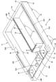
(基板21)
基板21は、長方形状であって、絶縁材料からなる絶縁板に銅箔等からなる導電路が印刷されたプリント基板とされており、バスバー40A〜40Cの接続部42が挿通される複数のスルーホール22と、ネジ67でネジ留めするための複数のネジ孔23A,23Bとが貫通形成されている。基板21は、放熱部材30の上面の縁部を除いた全面に重ねられており、図示しない複数の電子部品が実装されている。複数の電子部品は、FET(Field Effect Transistor)、コイル、コンデンサ、抵抗等からなる。
(Substrate 21)
The
内枠部56は、図6に示すように、L字状に曲がってバスバー40Bが圧入される圧入孔58を有する内枠本体60と、台座部52と連結される連結部61とを有する。
外枠部51の下面(裏面)には、四隅の位置に、基板21に載置される複数の載置部63が形成されている。複数の載置部63は、円柱状であって、下方(基板21側)に突出している。なお、載置部63の形状は円柱状に限られず、例えば、角柱状としたり、外枠部51の延びる方向に沿って延びる長尺の形状としてもよい。載置部63の下面(裏面)には、図5に示すように、下方からネジ67でネジ留め可能な留め部64が形成されている。留め部64には、基板21のネジ孔23Bを通ったネジ67の軸部がネジ留めされるネジ孔が形成されている。
As shown in FIG. 6, the
On the lower surface (back surface) of the
Priority Applications (6)
| Application Number | Priority Date | Filing Date | Title |
|---|---|---|---|
| JP2017094551A JP2018190914A (en) | 2017-05-11 | 2017-05-11 | Circuit structure and electric connection box |
| DE112018002422.9T DE112018002422T5 (en) | 2017-05-11 | 2018-04-25 | Circuit arrangement and electrical distribution box |
| US16/611,522 US10893611B2 (en) | 2017-05-11 | 2018-04-25 | Circuit assembly and electrical junction box |
| PCT/JP2018/016717 WO2018207621A1 (en) | 2017-05-11 | 2018-04-25 | Circuit configuration and electrical connection box |
| KR1020197032491A KR102287797B1 (en) | 2017-05-11 | 2018-04-25 | circuit assembly and electrical junction box |
| CN201880027498.7A CN110915312B (en) | 2017-05-11 | 2018-04-25 | Circuit structure and electrical connection box |
Applications Claiming Priority (1)
| Application Number | Priority Date | Filing Date | Title |
|---|---|---|---|
| JP2017094551A JP2018190914A (en) | 2017-05-11 | 2017-05-11 | Circuit structure and electric connection box |
Publications (2)
| Publication Number | Publication Date |
|---|---|
| JP2018190914A JP2018190914A (en) | 2018-11-29 |
| JP2018190914A5 true JP2018190914A5 (en) | 2019-11-07 |
Family
ID=64104499
Family Applications (1)
| Application Number | Title | Priority Date | Filing Date |
|---|---|---|---|
| JP2017094551A Pending JP2018190914A (en) | 2017-05-11 | 2017-05-11 | Circuit structure and electric connection box |
Country Status (6)
| Country | Link |
|---|---|
| US (1) | US10893611B2 (en) |
| JP (1) | JP2018190914A (en) |
| KR (1) | KR102287797B1 (en) |
| CN (1) | CN110915312B (en) |
| DE (1) | DE112018002422T5 (en) |
| WO (1) | WO2018207621A1 (en) |
Cited By (1)
| Publication number | Priority date | Publication date | Assignee | Title |
|---|---|---|---|---|
| JP7426861B2 (en) | 2020-03-17 | 2024-02-02 | 古河電気工業株式会社 | Busbar with electrical junction box and holder |
Families Citing this family (7)
| Publication number | Priority date | Publication date | Assignee | Title |
|---|---|---|---|---|
| JP6919599B2 (en) * | 2018-03-05 | 2021-08-18 | 住友電装株式会社 | Electrical junction box |
| JP2022161399A (en) * | 2021-04-09 | 2022-10-21 | 住友電装株式会社 | Electric connection box |
| JP2022161400A (en) * | 2021-04-09 | 2022-10-21 | 住友電装株式会社 | Electric connection box |
| JP2022161397A (en) * | 2021-04-09 | 2022-10-21 | 住友電装株式会社 | Electric connection box |
| JP2022161398A (en) * | 2021-04-09 | 2022-10-21 | 住友電装株式会社 | Electric connection box |
| JP2022161402A (en) * | 2021-04-09 | 2022-10-21 | 住友電装株式会社 | Electric connection box |
| JP2022161401A (en) * | 2021-04-09 | 2022-10-21 | 住友電装株式会社 | Electric connection box |
Family Cites Families (15)
| Publication number | Priority date | Publication date | Assignee | Title |
|---|---|---|---|---|
| JPS52134066U (en) | 1976-04-06 | 1977-10-12 | ||
| JPH0515035A (en) * | 1991-07-04 | 1993-01-22 | Fujikura Ltd | Electric connection box |
| JPH1141749A (en) | 1997-07-17 | 1999-02-12 | Yazaki Corp | Bus-bar fixing structure |
| JP3521115B2 (en) * | 1998-06-16 | 2004-04-19 | 矢崎総業株式会社 | Electronic unit wiring structure |
| JP3917473B2 (en) * | 2002-06-21 | 2007-05-23 | 株式会社オートネットワーク技術研究所 | Power module |
| JP2008125190A (en) * | 2006-11-09 | 2008-05-29 | Auto Network Gijutsu Kenkyusho:Kk | Electrical connection box |
| JP2009131017A (en) * | 2007-11-22 | 2009-06-11 | Yaskawa Electric Corp | Bus-bar support and motor controller using it |
| JP4974173B2 (en) * | 2007-12-28 | 2012-07-11 | 古河電気工業株式会社 | Electrical junction box |
| JP5679959B2 (en) | 2011-12-27 | 2015-03-04 | 三菱電機株式会社 | Current assist assembly using current assist members |
| JP2014011929A (en) * | 2012-07-03 | 2014-01-20 | Yazaki Corp | Electric connection box |
| JP5975070B2 (en) * | 2014-07-16 | 2016-08-23 | 株式会社オートネットワーク技術研究所 | Electrical junction box |
| JP6252871B2 (en) * | 2015-01-16 | 2017-12-27 | 株式会社オートネットワーク技術研究所 | Circuit structure and electrical junction box |
| JP6585359B2 (en) | 2015-03-25 | 2019-10-02 | 株式会社タムラ製作所 | Terminal unit and reactor |
| JP6614451B2 (en) * | 2016-06-08 | 2019-12-04 | 株式会社オートネットワーク技術研究所 | Board unit |
| US10368465B2 (en) * | 2017-09-07 | 2019-07-30 | Lear Corporation | Electrical unit |
-
2017
- 2017-05-11 JP JP2017094551A patent/JP2018190914A/en active Pending
-
2018
- 2018-04-25 DE DE112018002422.9T patent/DE112018002422T5/en active Granted
- 2018-04-25 KR KR1020197032491A patent/KR102287797B1/en active IP Right Grant
- 2018-04-25 US US16/611,522 patent/US10893611B2/en active Active
- 2018-04-25 WO PCT/JP2018/016717 patent/WO2018207621A1/en active Application Filing
- 2018-04-25 CN CN201880027498.7A patent/CN110915312B/en active Active
Cited By (1)
| Publication number | Priority date | Publication date | Assignee | Title |
|---|---|---|---|---|
| JP7426861B2 (en) | 2020-03-17 | 2024-02-02 | 古河電気工業株式会社 | Busbar with electrical junction box and holder |
Similar Documents
| Publication | Publication Date | Title |
|---|---|---|
| JP2018190914A5 (en) | ||
| US7969742B2 (en) | Bracket for mounting heat sink | |
| EP1995775A3 (en) | Semiconductor device with stress reducing element | |
| DE602008003166D1 (en) | SHIELDING AND HEAT DISPOSING DEVICE | |
| WO2018207621A1 (en) | Circuit configuration and electrical connection box | |
| JP2016015822A5 (en) | ||
| WO2008014325A3 (en) | An assembly for mounting electronic components, methods of use and manfacture thereof | |
| JP2011155056A (en) | Shielding structure | |
| JP2016152399A5 (en) | ||
| KR20180060572A (en) | Device package having heat dissipating member and the manufacturing method thereof | |
| JP6652144B2 (en) | Electronic parts, manufacturing method of electronic parts, mechanical parts | |
| JP5803961B2 (en) | Substrate spacing member and inverter device | |
| JPH0736468U (en) | Heat dissipation structure for electronic components | |
| WO2016115702A1 (en) | Heat dissipation apparatus for small-size device and circuit board heat dissipation system | |
| JP6230799B2 (en) | Control device | |
| WO2009063546A1 (en) | Heatsink | |
| JP2015135889A (en) | Capacitor | |
| JP2019197855A (en) | Circuit structure and electric connection box | |
| WO2014147681A1 (en) | Populated board, pressing member, and electronic device | |
| JP2000244080A (en) | Printed wiring board | |
| JP2011014837A5 (en) | ||
| JP6895065B2 (en) | Electronic component mounts and power supplies | |
| JP6789031B2 (en) | Heat dissipation structure | |
| US20140313674A1 (en) | Electronic device with heat sink | |
| JP3195849U (en) | Printed circuit board fixing device and apparatus using printed circuit board fixing device |