JP2018167166A - Light irradiation device and photo-curing device including the same - Google Patents
Light irradiation device and photo-curing device including the same Download PDFInfo
- Publication number
- JP2018167166A JP2018167166A JP2017065793A JP2017065793A JP2018167166A JP 2018167166 A JP2018167166 A JP 2018167166A JP 2017065793 A JP2017065793 A JP 2017065793A JP 2017065793 A JP2017065793 A JP 2017065793A JP 2018167166 A JP2018167166 A JP 2018167166A
- Authority
- JP
- Japan
- Prior art keywords
- light source
- light
- source unit
- led elements
- ultraviolet led
- Prior art date
- Legal status (The legal status is an assumption and is not a legal conclusion. Google has not performed a legal analysis and makes no representation as to the accuracy of the status listed.)
- Pending
Links
Images


Landscapes
- Led Device Packages (AREA)
- Physical Or Chemical Processes And Apparatus (AREA)
Abstract
【課題】光源をLED素子で構成した場合であっても、簡易な構成で所定の材料を十分に光硬化させることのできる光照射装置を提供する。【解決手段】 本発明は、所定の第一方向に搬送されるワークに対して光を照射する光照射装置であって、複数の第一紫外LED素子が平面上に配置されてなる第一光源部と、第一光源部に対して第一方向に隣接した位置において、複数の第二紫外LED素子が平面上に配列されてなる第二光源部とを有する。複数の第一紫外LED素子と、複数の第二紫外LED素子とは、同一条件下で点灯させたときに主たる発光波長が同一であり、第一光源部の温度特性と第二光源部の温度特性とが異なっている。【選択図】 図3Provided is a light irradiation device capable of sufficiently photocuring a predetermined material with a simple configuration even when the light source is configured by an LED element. The present invention is a light irradiation device for irradiating light to a workpiece conveyed in a predetermined first direction, and a first light source in which a plurality of first ultraviolet LED elements are arranged on a plane. And a second light source part in which a plurality of second ultraviolet LED elements are arranged on a plane at a position adjacent to the first light source part in the first direction. The plurality of first ultraviolet LED elements and the plurality of second ultraviolet LED elements have the same main emission wavelength when turned on under the same conditions, and the temperature characteristics of the first light source unit and the temperature of the second light source unit The characteristics are different. [Selection] Figure 3
Description
本発明は光照射装置に関し、特に紫外光を照射する装置に関する。また、本発明は、この光照射装置を備えた光硬化装置に関する。 The present invention relates to a light irradiation apparatus, and more particularly to an apparatus that irradiates ultraviolet light. Moreover, this invention relates to the photocuring apparatus provided with this light irradiation apparatus.
光エネルギーの作用で液状体から固体に変化させる技術を「光硬化」と呼び、インク、接着剤などのあらゆる分野で利用されている。例えば、下記特許文献1には、ワークの表面に塗布されたインクに対して光を照射されることで、インクが硬化して印字される画像形成装置が開示されている。
The technique of changing from a liquid to a solid by the action of light energy is called “photocuring” and is used in various fields such as ink and adhesives. For example,
特許文献1に記載されている画像形成装置では、紫外線エネルギーの付与によって硬化(重合化)する成分(主剤)と、重合開始剤とを含有したインクが用いられる。重合開始剤は光を吸収しやすい性質を有し、光が照射されると定められた過程を経てラジカルと呼ばれる非常に不安定な状態になる(下記式1)。
In the image forming apparatus described in
I→I*→R・ (1)
なお、上記式(1)において、Iは重合開始剤を示し、I*は重合開始剤が励起状態にあることを示し、R・はフリーラジカルを示す。重合開始剤に所定の光が照射されると、重合開始剤は励起され、開裂し、ラジカルを発生する。
I → I * → R ・ (1)
In the above formula (1), I represents a polymerization initiator, I * represents that the polymerization initiator is in an excited state, and R. represents a free radical. When the polymerization initiator is irradiated with predetermined light, the polymerization initiator is excited and cleaved to generate radicals.
発生したラジカルは、主剤に含まれるモノマーの二重結合と反応して連鎖反応種を生成する(下記式2,3)。
The generated radical reacts with the double bond of the monomer contained in the main agent to generate a chain reaction species (the following
R・+M→RM・ (2)
RM・+M→RMM・ (3)
上記式(2)、(3)において、Mはモノマーを示す。
R ・ + M → RM ・ (2)
RM ・ + M → RMM ・ (3)
In the above formulas (2) and (3), M represents a monomer.
連鎖反応種が成長反応へと進み、ポリマー鎖を生成する(下記式4)。下記式において、Pm、Pnはポリマーを示す。
RMm・+RMn・→Pm+Pn (4)
The chain reaction species proceeds to the growth reaction, and a polymer chain is generated (Formula 4 below). In the following formulae, P m and P n represent polymers.
RM m + RM n → P m + P n (4)
上記式(1)〜(4)を経て、重合反応が進行し、インクが硬化されることで、ワーク(例えば紙)の上面に印字が行われる。 Through the above formulas (1) to (4), the polymerization reaction proceeds and the ink is cured, whereby printing is performed on the upper surface of the workpiece (for example, paper).
上記特許文献1にも記載されているように、従来、光硬化装置用の光源としてはランプが用いられていた。しかし、近年、発光波長が紫外域を示す半導体発光素子の開発が進展し、その出力が向上しつつあることから、光源として、ランプから、ランプよりも長寿命が期待できるLED素子への置換が考えられている。
As described in
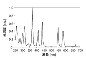
ところで、上記(1)式の反応を生じさせるべく、光硬化装置に用いられる光源は、その発光波長が重合開始剤の吸収スペクトルに適したものを採用することが要求される。LED素子の発光波長の帯域幅は、ランプのそれよりも狭い。このため、本発明者(ら)は、LED素子の発光波長をどの程度にするべきかを検討すべく、まず、従来用いられていた光硬化用のインクに添加されていた重合性化合物及び重合開始剤の吸収スペクトルを分析した。この吸収スペクトルの一例を図8に示す。図8において、横軸は波長を示し、縦軸は吸光度を示す。なお、図8では、重合性化合物として、フェノキシアクリレート、トリプロピレングリコールジアクリレート、トリシクロデカンジメタノールジアクリレートを含む材料を採用した。また、重合開始剤として、ビス(2,4,6−トリメチルベンゾイル)−フェニルフォスフィンオキサイド、2,4,6−トリメチルベンゾイル−ジフェニル−フォスフィンオキサイドを含む材料を採用した。 By the way, in order to cause the reaction of the above formula (1), it is required that the light source used in the photocuring apparatus adopts an emission wavelength suitable for the absorption spectrum of the polymerization initiator. The bandwidth of the emission wavelength of the LED element is narrower than that of the lamp. For this reason, in order to examine how much the emission wavelength of the LED element should be, the present inventors (e.g.) firstly added a polymerizable compound and a polymerization agent that were added to the conventionally used photo-curing ink. The absorption spectrum of the initiator was analyzed. An example of this absorption spectrum is shown in FIG. In FIG. 8, the horizontal axis indicates the wavelength, and the vertical axis indicates the absorbance. In FIG. 8, a material containing phenoxy acrylate, tripropylene glycol diacrylate, and tricyclodecane dimethanol diacrylate was employed as the polymerizable compound. As the polymerization initiator, a material containing bis (2,4,6-trimethylbenzoyl) -phenylphosphine oxide and 2,4,6-trimethylbenzoyl-diphenyl-phosphine oxide was employed.
また、この重合性化合物及び重合開始剤を含むインクの硬化用光源として用いられていたランプの発光スペクトルの一例を図9に示す。図9において、横軸は波長を示し、縦軸は光強度の相対値を示す。 FIG. 9 shows an example of an emission spectrum of a lamp used as a light source for curing the ink containing the polymerizable compound and the polymerization initiator. In FIG. 9, the horizontal axis indicates the wavelength, and the vertical axis indicates the relative value of the light intensity.
図8に示すように、重合性化合物や重合開始剤の吸収スペクトルは比較的帯域幅が広いことが確認された。また、図9に示される発光スペクトルによれば、図8に示す、重合性化合物及び重合開始剤の吸収スペクトルと重なりを有していることが確認された。よって、図9に示すスペクトルを示す光を射出するランプを光源として用いることで、ランプからの射出光が重合開始剤に効率よく吸収され、重合反応が進行することが予想される。 As shown in FIG. 8, it was confirmed that the absorption spectra of the polymerizable compound and the polymerization initiator have a relatively wide bandwidth. Further, according to the emission spectrum shown in FIG. 9, it was confirmed that there was an overlap with the absorption spectra of the polymerizable compound and the polymerization initiator shown in FIG. 8. Therefore, by using a lamp that emits light having a spectrum shown in FIG. 9 as a light source, it is expected that the light emitted from the lamp is efficiently absorbed by the polymerization initiator and the polymerization reaction proceeds.
次に、光源をランプからLED素子に置換することを検討する。LED素子の発光スペクトルはランプよりも狭帯域となることが知られている。そこで、本発明者は、LED素子の発光スペクトルのピーク波長が、重合開始剤の吸収スペクトルのピーク波長にほぼ等しくなるようにLED素子を選択することを検討した。具体的には、図8に示す例であれば、発光スペクトルのピーク波長が、365nmを示すLED素子を光硬化用光源として選択した。 Next, consider replacing the light source with a LED element from the lamp. It is known that the emission spectrum of the LED element is narrower than that of the lamp. Therefore, the present inventor has studied to select an LED element so that the peak wavelength of the emission spectrum of the LED element is substantially equal to the peak wavelength of the absorption spectrum of the polymerization initiator. Specifically, in the example shown in FIG. 8, an LED element having an emission spectrum peak wavelength of 365 nm was selected as a light source for photocuring.
しかし、上記LED素子によって光源を設計した場合、従来のランプと比較して、硬化が不十分であることが確認された。本発明者は、この理由を以下のように推察している。 However, when the light source was designed with the LED element, it was confirmed that the curing was insufficient as compared with the conventional lamp. The inventor presumes this reason as follows.
LED素子の発光スペクトルは、従来用いられていた重合開始剤の吸収スペクトルに比べて帯域幅が極めて狭い。また、上述したように、LED素子の発光スペクトルは、ランプの発光スペクトルに比べても帯域幅が狭い。従来の重合開始剤に対してランプからの光を照射すると、この重合開始剤は、原理的に、吸収スペクトルのピーク波長成分の光のみならず、当該ピークから少し離れた波長成分の光も吸収する。 The emission spectrum of the LED element has a very narrow bandwidth compared to the absorption spectrum of a polymerization initiator that has been conventionally used. Further, as described above, the emission spectrum of the LED element has a narrower bandwidth than the emission spectrum of the lamp. When a conventional polymerization initiator is irradiated with light from a lamp, in principle, this polymerization initiator absorbs not only light having a peak wavelength component in the absorption spectrum but also light having a wavelength component slightly away from the peak. To do.
ワークの表面に塗布された未硬化のインクは、ある程度の径(大きさ)を有する。このため、インクに含まれる重合開始剤についても、インクの外表面に存在するものもあれば、インクの内部付近に存在するものもある。LED素子の発光スペクトルは狭帯域であるため、波長によっては、インクの表面付近に存在する重合開始剤には光が十分に吸収されるものの、インク内部付近に存在する重合開始剤には光が十分に吸収されないことが想定される。また、逆に、インクの内部付近に存在する重合開始剤には光が十分に吸収されるものの、インク表面付近に存在する重合開始剤には光が十分に吸収されないことが想定される。 The uncured ink applied to the surface of the work has a certain diameter (size). For this reason, some of the polymerization initiators contained in the ink are present on the outer surface of the ink, while others are present in the vicinity of the inside of the ink. Since the emission spectrum of the LED element is narrow, depending on the wavelength, the polymerization initiator present near the ink surface absorbs light sufficiently, but the polymerization initiator present near the ink has light. It is assumed that it is not sufficiently absorbed. Conversely, it is assumed that light is sufficiently absorbed by the polymerization initiator present near the inside of the ink, but light is not sufficiently absorbed by the polymerization initiator present near the ink surface.
なお、重合開始剤には、吸収スペクトルの帯域幅が比較的狭いものも存在する。従って、このような重合開始剤が添加されたインクを用いることで、LED素子からの射出光であっても十分に硬化できる可能性がある。しかしながら、従来用いていたインクから他のインクに置き換えた場合、印字後の色味が変化してしまうおそれがあることから、従来のインクを引き続き使用したいというユーザの要請が存在する。このため、光源に応じて適したインクに置き換えることは、市場の需要に鑑みるとあまり好ましいことではない。 Some polymerization initiators have a relatively narrow absorption spectrum bandwidth. Therefore, by using the ink to which such a polymerization initiator is added, there is a possibility that the light emitted from the LED element can be sufficiently cured. However, when the ink used in the past is replaced with another ink, there is a possibility that the color after printing may change, and there is a user's request to continue using the conventional ink. For this reason, replacing with a suitable ink according to the light source is not very preferable in view of market demand.
また、別の方法として、発光波長の異なる複数のLED素子を光源に配置するという方法が考えられる。例えば、図8に示す吸収スペクトルを示す重合開始剤が添加されたインクであれば、ピーク波長が365nm、385nm、405nmを示す複数のLED素子を光源に備えることが考えられる。しかし、発光波長の異なるLED素子は、相互に組成が異なっており発光特性が異なる。このため、これらのLED素子に対して共通の電源や配線で実装することができない。つまり、発光波長ごとに電源や配線を分けて配置する必要があるため、機構が複雑化してしまう。 As another method, a method of arranging a plurality of LED elements having different emission wavelengths in a light source is conceivable. For example, in the case of an ink to which a polymerization initiator having an absorption spectrum shown in FIG. 8 is added, it is conceivable that the light source includes a plurality of LED elements having peak wavelengths of 365 nm, 385 nm, and 405 nm. However, LED elements having different emission wavelengths have different compositions and different emission characteristics. For this reason, these LED elements cannot be mounted with a common power source or wiring. That is, since it is necessary to separately arrange the power source and wiring for each emission wavelength, the mechanism becomes complicated.
本発明は上記の課題に鑑み、光源をLED素子で構成した場合であっても、簡易な構成で所定の材料を十分に光硬化させることのできる光照射装置を提供することを目的とする。また、本発明は、このような光照射装置を含む光硬化装置を実現することを目的とする。 In view of the above problems, an object of the present invention is to provide a light irradiation apparatus capable of sufficiently photocuring a predetermined material with a simple configuration even when the light source is configured by an LED element. Moreover, an object of this invention is to implement | achieve the photocuring apparatus containing such a light irradiation apparatus.
本発明は、所定の第一方向に搬送されるワークに対して光を照射する光照射装置であって、
複数の第一紫外LED素子が配置されてなる第一光源部と、
前記第一光源部に対して前記第一方向に隣接した位置において、複数の第二紫外LED素子が配置されてなる第二光源部とを有し、
複数の前記第一紫外LED素子と、複数の前記第二紫外LED素子とは、同一条件下で点灯させたときに主たる発光波長が同一であり、
前記第一光源部の温度特性と前記第二光源部の温度特性とが異なっていることを特徴とする。
The present invention is a light irradiation device for irradiating light to a workpiece conveyed in a predetermined first direction,
A first light source unit in which a plurality of first ultraviolet LED elements are disposed;
A second light source part in which a plurality of second ultraviolet LED elements are arranged at a position adjacent to the first light source part in the first direction;
The plurality of first ultraviolet LED elements and the plurality of second ultraviolet LED elements have the same main emission wavelength when lit under the same conditions,
The temperature characteristics of the first light source unit and the temperature characteristics of the second light source unit are different.
上記構成によれば、第一光源部と第二光源部に備えられた紫外LED素子は、いずれも同一条件下で点灯させたときの主たる発光波長が同一である。このため、電源や配線を共通化した状態で発光させることができる。そして、第一光源部と第二光源部の温度特性が異なっているため、上記のように電源や配線を共通化して発光させたとしても、両光源部の温度環境が異なるため、各光源部から射出される光の波長を相互に異ならせることができる。 According to the said structure, as for the ultraviolet LED element with which the 1st light source part and the 2nd light source part were equipped, the main light emission wavelength when all are made to light on the same conditions is the same. For this reason, it is possible to emit light with the power supply and the wiring shared. Since the temperature characteristics of the first light source unit and the second light source unit are different, even if the power source and the wiring are made common to emit light as described above, the temperature environment of both the light source units is different. The wavelengths of light emitted from each other can be made different from each other.
特に、第一光源部と第二光源部は、ワークの搬送方向である第一方向に隣接した位置に配置されている。つまり、ワーク上の同一の箇所に対して、第一光源部から射出された光と、第二光源部から射出された光とが照射される。このため、ワーク上に載置されたインクに添付されている重合開始剤に対して、異なる波長の光を照射させることができる。これにより、インクの全体にわたって光を届かせることができるため、全体にわたって重合反応が促進され、十分に硬化させることができる。 In particular, the first light source unit and the second light source unit are arranged at positions adjacent to the first direction, which is the workpiece transfer direction. That is, the light emitted from the first light source unit and the light emitted from the second light source unit are irradiated to the same location on the workpiece. For this reason, the light of a different wavelength can be irradiated with respect to the polymerization initiator attached to the ink mounted on the workpiece | work. Thereby, since light can reach over the whole ink, a polymerization reaction is promoted over the whole and it can fully harden | cure.
光照射装置は、第一光源部と第二光源部以外に、第一光源部及び第二光源部に対して更に温度が異なる別の光源部を、第一方向に沿って配置するものとしても構わない。 In addition to the first light source unit and the second light source unit, the light irradiation device may be arranged with another light source unit having a different temperature from the first light source unit and the second light source unit along the first direction. I do not care.
上記において、第一紫外LED素子と第二紫外LED素子とが、同一条件下で点灯させたときに主たる発光波長が同一であると記載した。ここで、発光波長が同一であるとは、同一の温度環境下で同一の電流量を注入して点灯させたときに両素子から発せられる光の主たるピーク波長の相違が、一般的な誤差範囲内に留められているものをいう。例えば、この誤差範囲とは、±20nmである。 In the above, it described that the 1st ultraviolet LED element and the 2nd ultraviolet LED element had the same main light emission wavelength when it was made to light on the same conditions. Here, the same emission wavelength means that the difference between the main peak wavelengths of light emitted from both elements when the same current amount is injected and lighted under the same temperature environment is a general error range. The one that is held inside. For example, this error range is ± 20 nm.
第一光源部の温度特性と第二光源部の温度特性を異ならせるための具体的な手段としては、以下の二つの方法が想定される。 As specific means for making the temperature characteristics of the first light source unit different from the temperature characteristics of the second light source unit, the following two methods are assumed.
第一の方法は、第一光源部と第二光源部の加熱の程度を異ならせることである。より具体的には、
前記第一光源部内において前記第一方向とは非平行な第二方向に配置された複数の前記第一紫外LED素子の配置密度と、前記第二光源部内において前記第二方向に配置された複数の前記第二紫外LED素子の配置密度とを異ならせる構成とすることができる。
The first method is to vary the degree of heating of the first light source unit and the second light source unit. More specifically,
An arrangement density of the plurality of first ultraviolet LED elements arranged in a second direction non-parallel to the first direction in the first light source unit, and a plurality arranged in the second direction in the second light source unit The arrangement density of the second ultraviolet LED element can be made different.
このような構成とすることで、紫外LED素子の配置密度が高い光源部の温度が上昇しやすくなり、配置密度が低い光源部の温度は上昇しにくくなる。このため、両光源部間に温度差を設けることができる。なお、第二方向は、ワークの面に平行な方向であるものとしてよい。更に、第二方向は、第一方向に直交する方向であるものとしても構わない。 By setting it as such a structure, the temperature of the light source part with a high arrangement density of an ultraviolet LED element becomes easy to rise, and the temperature of the light source part with a low arrangement density becomes difficult to rise. For this reason, a temperature difference can be provided between both light source parts. The second direction may be a direction parallel to the surface of the workpiece. Furthermore, the second direction may be a direction orthogonal to the first direction.
第二の方法は、第一光源部と第二光源部の冷却性能を異ならせることである。より具体的には、
前記第一光源部は、複数の前記第一紫外LED素子を主面上に配置した第一実装基板と、前記第一実装基板の主面とは反対側の面に連絡して設けられた第一ヒートシンクとを有し、
前記第二光源部は、複数の前記第二紫外LED素子を主面上に配置した第二実装基板と、前記第二実装基板の主面とは反対側の面に連絡して設けられ、前記第一ヒートシンクと冷却能力の異なる第二ヒートシンクとを有する構成とすることができる。
The second method is to vary the cooling performance of the first light source unit and the second light source unit. More specifically,
The first light source unit is provided in contact with a first mounting substrate in which a plurality of the first ultraviolet LED elements are arranged on a main surface, and a surface opposite to the main surface of the first mounting substrate. One heat sink,
The second light source unit is provided in contact with a second mounting substrate in which a plurality of the second ultraviolet LED elements are arranged on a main surface, and a surface opposite to the main surface of the second mounting substrate, It can be set as the structure which has a 1st heat sink and the 2nd heat sink from which cooling capacity differs.
第一ヒートシンクと第二ヒートシンクで冷却能力を異ならせるためには、種々の具体的な方法が考えられる。第一ヒートシンクと第二ヒートシンクで厚みを異ならせるものとしても構わない。第一ヒートシンクと第二ヒートシンクの双方を水冷機構とし、流通させる水の流量や経路を異ならせるものとしても構わない。第一ヒートシンクと第二ヒートシンクの双方を空冷機構とし、フィンの数や厚みを異ならせるものとしても構わない。更に、第一ヒートシンク及び第二ヒートシンクにファンを設け、このファンの能力を異ならせるものとしても構わない。 In order to make the cooling capacity different between the first heat sink and the second heat sink, various specific methods are conceivable. The thickness may be different between the first heat sink and the second heat sink. Both the first heat sink and the second heat sink may be water cooling mechanisms, and the flow rate and path of water to be circulated may be different. Both the first heat sink and the second heat sink may be air cooling mechanisms, and the number and thickness of the fins may be different. Further, fans may be provided on the first heat sink and the second heat sink, and the capabilities of the fans may be different.
本発明の光硬化装置は、上記の光照射装置を備え、
前記第一方向に搬送される前記ワークの表面には所定の材料物が塗布されており、
前記第一光源部及び前記第二光源部から前記ワークに対して光が照射されることで、前記材料物が硬化されることを特徴とする。
The photocuring device of the present invention comprises the above light irradiation device,
A predetermined material is applied to the surface of the workpiece conveyed in the first direction,
The material is cured by irradiating the workpiece with light from the first light source unit and the second light source unit.
光硬化装置の一例として、画像形成装置を構成することができる。この画像形成装置は、搬送されるワークの一方の面に、光が照射されると硬化する塗料やインクなどの材料物が塗布されており、光照射装置から射出される光が照射されることでこの材料物が硬化し、ワークの面に画像が形成される。ワークとしては、樹脂シート、フィルム、布、プリント基板、紙など、材質や形状を問わず種々のものを利用することができる。 An image forming apparatus can be configured as an example of a photocuring apparatus. In this image forming apparatus, a material such as paint or ink that is cured when irradiated with light is applied to one surface of a conveyed work, and light emitted from the light irradiation apparatus is irradiated. This material is cured and an image is formed on the surface of the workpiece. As a workpiece, various materials such as a resin sheet, a film, a cloth, a printed board, and paper can be used regardless of the material and shape.
本発明によれば、光源をLED素子で構成しながらも、簡易な構成で所定の材料を十分に光硬化させることのできる光照射装置が実現される。 ADVANTAGE OF THE INVENTION According to this invention, the light irradiation apparatus which can fully photocure a predetermined material with a simple structure is implement | achieved, although comprising a light source with an LED element.
本発明の光照射装置及び光硬化装置の実施形態につき、図面を参照して説明する。なお、以下の各図面は、あくまで模式的に図示されたものであり、図面の寸法比と実際の寸法比は必ずしも一致しない。 Embodiments of a light irradiation device and a photocuring device of the present invention will be described with reference to the drawings. Note that the following drawings are only schematically shown, and the dimensional ratios in the drawings do not necessarily match the actual dimensional ratios.
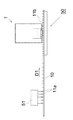
図1は、光硬化装置の構成を模式的に示す図面である。光硬化装置50は、光照射装置1と、その上流側に配置された材料物塗布部51とを備えている。光照射装置1は、紫外光を発するLED素子を光源として含む。材料物塗布部51は、ワーク10の上面の所定の箇所に、材料物11aを塗布する。例えば、光硬化装置50が画像形成装置で構成される場合には、ワーク10の上面に形成したい画像情報に応じて決定される、ワーク10の上面の所定の箇所に、材料物塗布部51が材料物11aを塗布する。
FIG. 1 is a drawing schematically showing a configuration of a photocuring apparatus. The
材料物塗布部51によって表面に材料物11aが塗布されたワーク10は、搬送方向D1に沿って搬送され、光照射装置1から射出された光が照射される。これにより、材料物11aが硬化され、硬化後の材料物11bがワーク10の上面に形成される。
The
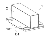
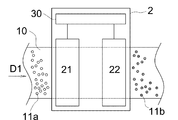
図2及び図3は、光照射装置1の構成を模式的に示す図面である。図2は、光照射装置1の斜視図に対応する。また、図3は光照射装置1の模式的なブロック図に対応する。
2 and 3 are drawings schematically showing the configuration of the
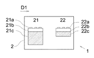
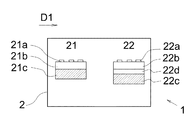
光照射装置1は、光照射ユニット2を備え、D1方向に搬送されるワーク10に対して光照射ユニット2が光を照射する。図3の例では、光照射ユニット2が、第一光源部21、第二光源部22、及び電源部30を備える構成が図示されている。第一光源部21及び第二光源部22は、それぞれ複数の紫外LED素子を含み、電源部30から電力が供給されることで発光する。第一光源部21と第二光源部22は、D1方向に隣接して配置されており、両者の温度特性が異なるように構成されている。
The
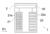
(第一実施形態)
図4は、光照射装置1の第一実施形態の構成を模式的に示す図面である。D1方向に隣接して配置された第一光源部21と第二光源部22において、D1方向に直交する方向、すなわちワーク10の幅方向に関して、紫外LED素子の配置密度を異ならせている。第一光源部21は、複数の紫外LED素子21a(第一紫外LED素子)を含み、第二光源部22は、複数の紫外LED素子22a(第二紫外LED素子)を含む構成である。これらの紫外LED素子21a及び22aは、同一条件下で点灯させたときに主たる発光波長が同一である素子である。言い換えれば、同一の特性を示すと認められる素子同士である。なお、以下では、「紫外LED素子」を単に「LED素子」と略記することがある。
(First embodiment)
FIG. 4 is a drawing schematically showing the configuration of the first embodiment of the
そして、図4の例では、上流側に位置する第一光源部21は、下流側に位置する第二光源部22よりも、配置されるLED素子の密度が低くなるように構成されている。LED素子の配置密度を高めることで、隣接するLED素子同士の間隔が狭まり、この結果、温度が上昇しやすくなる。すなわち、光照射時において、第二光源部22は、第一光源部21よりも温度が高くなる。この結果、第二光源部22から照射される光は、第一光源部21から照射される光よりも波長が長くなる。
And in the example of FIG. 4, the 1st
上述したように、第一光源部21と第二光源部22は、ワーク10の搬送方向D1に沿って隣接して配置されている。このため、ワーク10が搬送されると、ワーク10上に塗布された材料物11aは、第一光源部21からの光が照射された後に、第二光源部22からの光が照射されることになる。この結果、異なる波長の光が照射されるため、材料物11aの全体に光が進行し、硬化の度合を高めることができる。
As described above, the first
なお、図5に示すように、上流側に位置する第一光源部21が備えるLED素子21aを高密度に配置し、下流側に位置する第二光源部22が備えるLED素子22aを低密度に配置するものとしても構わない。
In addition, as shown in FIG. 5, the
他の例として、光照射ユニット2は、第一光源部21及び第二光源部22をD1方向に沿って複数組備えるものとしても構わない。また、光照射ユニット2は、第一光源部21及び第二光源部22以外に、これらとは更にLED素子の配置密度を異ならせた光源部を備えるものとしても構わない。
As another example, the
(第二実施形態)
図6は、光照射装置1の第二実施形態の構成を模式的に示す図面である。本実施形態では、D1方向に隣接して配置された第一光源部21と第二光源部22において、冷却能力を異ならせている。
(Second embodiment)
FIG. 6 is a drawing schematically showing the configuration of the second embodiment of the
より詳細には、第一光源部21は、複数の第一紫外LED素子21aを主面上に配置した第一実装基板21bと、第一実装基板21bの主面とは反対側の面に連絡して設けられた第一ヒートシンク21cとを有する。同様に、第二光源部22は、複数の第二紫外LED素子22aを主面上に配置した第二実装基板22bと、第二実装基板22bの主面とは反対側の面に連絡して設けられた第二ヒートシンク22cとを有する。
More specifically, the first
そして、図6の例では、第一ヒートシンク21cと第二ヒートシンク22cとの厚みが異なっており、これによって、両者の冷却能力に差を生じさせている。より詳細には、第一ヒートシンク21cの厚みを第二ヒートシンク22cよりも厚くすることで、第一ヒートシンク21cの方が第二ヒートシンク22cよりも高い冷却能力を有するように構成されている。
In the example of FIG. 6, the
このような構成とすることで、第一発光部21の方が第二発光部22よりも冷却されやすくなるため、光照射時において、第二光源部22は、第一光源部21よりも温度が高くなる。この結果、第二光源部22から照射される光は、第一光源部21から照射される光よりも波長が長くなり、第一実施形態と同様の効果を実現することができる。
By adopting such a configuration, the first
第一ヒートシンク21cと第二ヒートシンク22cとで冷却能力を異ならせる方法としては、種々の方法を採用することができる。図7は別の例を示す模式的な図面であり、第二ヒートシンク22cと第二実装基板22bとの間に、熱伝導率の低い材料層22dを設けている。この構成により、第二ヒートシンク22cは、第一ヒートシンク21cよりも冷却能力が低下する。
Various methods can be adopted as a method of making the cooling capacity different between the
また、別の例として、第一ヒートシンク21cと第二ヒートシンク22cを共に水冷方式のヒートシンクとし、第一ヒートシンク21c内に流通させる水量を、第二ヒートシンク22c内に流通させる水量よりも高めることで、第一ヒートシンク21cを第二ヒートシンク22cよりも冷却能力を高める構成とすることもできる。
As another example, both the
また、別の例として、第一ヒートシンク21cと第二ヒートシンク22cを共に空冷方式のヒートシンクとし、第一ヒートシンク21cを第二ヒートシンク22cよりもフィンの数を増やす態様も可能である。
As another example, the
更に別の例として、第一ヒートシンク21c側に設けられたファンの出力を、第二ヒートシンク22c側に設けられたファンの出力よりも高める態様も可能である。
As yet another example, a mode in which the output of the fan provided on the
なお、上記の実施形態では、第一ヒートシンク21cを第二ヒートシンク22cよりも冷却能力を高めた場合について説明したが、逆に、第二ヒートシンク22cを第一ヒートシンク21cよりも冷却能力を高めた構成を採用しても構わない。
In the above embodiment, the case where the
第二実施形態においても、光照射ユニット2は、第一光源部21及び第二光源部22をD1方向に沿って複数組備える構成としても構わない。また、光照射ユニット2は、第一光源部21及び第二光源部22以外に、これらとは更に冷却能力を異ならせたヒートシンクを含む光源部を備えるものとしても構わない。
Also in 2nd embodiment, the
[別実施形態]
以下、別実施形態につき説明する。
[Another embodiment]
Hereinafter, another embodiment will be described.
〈1〉 第一実施形態では、第一光源部21と第二光源部22とで、LED素子の配置密度を異ならせることで発熱の程度を異ならせ、これによって温度環境を異ならせていた。これに対し、第一光源部21と第二光源部22とにおいて、LED素子の配置密度を同一にしながら、注入電流量を異ならせることで発熱の程度を異ならせることで、温度環境を異ならせるものとしても構わない。
<1> In the first embodiment, the first
〈2〉 上記の実施形態では、第一光源部21及び第二光源部22は、いずれもD1方向に沿って複数列(図面上は3列)のLED素子が配置されているものとしたが、この列数は1でも構わない。
<2> In the above-described embodiment, the first
〈3〉 第二実施形態において、上述した図面では、第一発光部21が備える第一紫外LED素子21aが実装されている基板と、第二発光部22が備える第二紫外LED素子22aが実装されている基板とが分離されているものとして説明したが、これらが同一の基板で構成されているものとしても構わない。
<3> In the second embodiment, in the above-described drawings, the substrate on which the first
1 : 光照射装置
2 : 光照射ユニット
10 : ワーク
11a : 材料物
11b : 硬化後の材料物
21 : 第一光源部
21a : 第一紫外LED素子
21b : 第一実装基板
21c : 第一ヒートシンク
22 : 第二光源部
22a : 第二紫外LED素子
22b : 第二実装基板
22c : 第二ヒートシンク
22d : 材料層
30 : 電源部
50 : 光硬化装置
51 : 材料物塗布部
D1 : 搬送方向
1: Light irradiation device 2: Light irradiation unit 10:
Claims (4)
複数の第一紫外LED素子が配置されてなる第一光源部と、
前記第一光源部に対して前記第一方向に隣接した位置において、複数の第二紫外LED素子が配置されてなる第二光源部とを有し、
複数の前記第一紫外LED素子と、複数の前記第二紫外LED素子とは、同一条件下で点灯させたときに主たる発光波長が同一であり、
前記第一光源部の温度特性と前記第二光源部の温度特性とが異なっていることを特徴とする光照射装置。 A light irradiation device that irradiates light to a workpiece conveyed in a predetermined first direction,
A first light source unit in which a plurality of first ultraviolet LED elements are disposed;
A second light source part in which a plurality of second ultraviolet LED elements are arranged at a position adjacent to the first light source part in the first direction;
The plurality of first ultraviolet LED elements and the plurality of second ultraviolet LED elements have the same main emission wavelength when lit under the same conditions,
The light irradiation apparatus, wherein the temperature characteristics of the first light source unit and the temperature characteristics of the second light source unit are different.
前記第二光源部は、複数の前記第二紫外LED素子を主面上に配置した第二実装基板と、前記第二実装基板の主面とは反対側の面に連絡して設けられ、前記第一ヒートシンクと冷却能力の異なる第二ヒートシンクとを有することを特徴とする請求項1に記載の光照射装置。 The first light source unit is provided in contact with a first mounting substrate in which a plurality of the first ultraviolet LED elements are arranged on a main surface, and a surface opposite to the main surface of the first mounting substrate. One heat sink,
The second light source unit is provided in contact with a second mounting substrate in which a plurality of the second ultraviolet LED elements are arranged on a main surface, and a surface opposite to the main surface of the second mounting substrate, The light irradiation apparatus according to claim 1, further comprising: a first heat sink and a second heat sink having different cooling capabilities.
前記第一方向に搬送される前記ワークの表面には所定の材料物が塗布されており、
前記第一光源部及び前記第二光源部から前記ワークに対して光が照射されることで、前記材料物が硬化されることを特徴とする光硬化装置。
The light irradiation apparatus according to any one of claims 1 to 3,
A predetermined material is applied to the surface of the workpiece conveyed in the first direction,
The photocuring apparatus, wherein the material is cured by irradiating the workpiece with light from the first light source unit and the second light source unit.
Priority Applications (1)
| Application Number | Priority Date | Filing Date | Title |
|---|---|---|---|
| JP2017065793A JP2018167166A (en) | 2017-03-29 | 2017-03-29 | Light irradiation device and photo-curing device including the same |
Applications Claiming Priority (1)
| Application Number | Priority Date | Filing Date | Title |
|---|---|---|---|
| JP2017065793A JP2018167166A (en) | 2017-03-29 | 2017-03-29 | Light irradiation device and photo-curing device including the same |
Publications (1)
| Publication Number | Publication Date |
|---|---|
| JP2018167166A true JP2018167166A (en) | 2018-11-01 |
Family
ID=64018401
Family Applications (1)
| Application Number | Title | Priority Date | Filing Date |
|---|---|---|---|
| JP2017065793A Pending JP2018167166A (en) | 2017-03-29 | 2017-03-29 | Light irradiation device and photo-curing device including the same |
Country Status (1)
| Country | Link |
|---|---|
| JP (1) | JP2018167166A (en) |
Cited By (5)
| Publication number | Priority date | Publication date | Assignee | Title |
|---|---|---|---|---|
| CN114617986A (en) * | 2020-12-11 | 2022-06-14 | 波音公司 | Ultraviolet light emitting assembly |
| US12023413B2 (en) | 2020-12-11 | 2024-07-02 | The Boeing Company | Ultraviolet light-emitting module and disinfecting system |
| US12053554B2 (en) | 2020-12-11 | 2024-08-06 | The Boeing Company | Ultraviolet light-emitting module and disinfecting system |
| US12165864B2 (en) | 2020-12-11 | 2024-12-10 | The Boeing Company | Ultraviolet light-emitting module and disinfecting system |
| US12377180B2 (en) | 2020-12-11 | 2025-08-05 | The Boeing Company | Ultraviolet light-emitting module and disinfecting system |
-
2017
- 2017-03-29 JP JP2017065793A patent/JP2018167166A/en active Pending
Cited By (7)
| Publication number | Priority date | Publication date | Assignee | Title |
|---|---|---|---|---|
| CN114617986A (en) * | 2020-12-11 | 2022-06-14 | 波音公司 | Ultraviolet light emitting assembly |
| EP4035690A3 (en) * | 2020-12-11 | 2022-10-26 | The Boeing Company | Ultraviolet light-emitting assembly |
| US12023413B2 (en) | 2020-12-11 | 2024-07-02 | The Boeing Company | Ultraviolet light-emitting module and disinfecting system |
| US12053554B2 (en) | 2020-12-11 | 2024-08-06 | The Boeing Company | Ultraviolet light-emitting module and disinfecting system |
| US12165864B2 (en) | 2020-12-11 | 2024-12-10 | The Boeing Company | Ultraviolet light-emitting module and disinfecting system |
| US12377180B2 (en) | 2020-12-11 | 2025-08-05 | The Boeing Company | Ultraviolet light-emitting module and disinfecting system |
| US12383640B2 (en) | 2020-12-11 | 2025-08-12 | The Boeing Company | Ultraviolet light-emitting assembly |
Similar Documents
| Publication | Publication Date | Title |
|---|---|---|
| JP2018167166A (en) | Light irradiation device and photo-curing device including the same | |
| US7642527B2 (en) | Multi-attribute light effects for use in curing and other applications involving photoreactions and processing | |
| ES2713862T3 (en) | Method for curing a substance, device for performing said method and ink | |
| US6457823B1 (en) | Apparatus and method for setting radiation-curable ink | |
| KR101985823B1 (en) | Light irradiation apparatus | |
| US8421043B2 (en) | Solid state radiation source array | |
| TWI640412B (en) | Curing device and method with multi-wavelength LED | |
| CN1980961A (en) | UV light for inkjet printers | |
| WO2004108417A1 (en) | Ink jet printer using uv ink | |
| JPWO2008078560A1 (en) | Inkjet recording device | |
| TW201350745A (en) | Deflectors for a lighting module | |
| JP2011233522A (en) | Exposure device having array of light-emitting diode | |
| US10261420B2 (en) | UV mask device and method for using the same | |
| US7461949B2 (en) | Methods and systems relating to solid state light sources for use in industrial processes | |
| JP6006379B2 (en) | Light irradiation device | |
| CN219271186U (en) | Light emitting module, light source and dental light curing machine | |
| JP3197315U (en) | Wrap-around window for lighting module | |
| US7684665B2 (en) | Methods and systems relating to solid state light sources for use in industrial processes | |
| KR20140128718A (en) | Cure unit and apparatus for manufacturing printend electronics adopting the same | |
| CN209534483U (en) | LED light curing device and inkjet printer | |
| JP7793066B2 (en) | light irradiation device | |
| JP6664135B2 (en) | 3D printer | |
| KR20120041479A (en) | Photolithography apparatus | |
| JP2017048263A (en) | Method for producing cured product of photocurable resin composition and light irradiation device | |
| JP2023016519A (en) | Light irradiation device and printing device |