JP2011233522A - Exposure device having array of light-emitting diode - Google Patents
Exposure device having array of light-emitting diode Download PDFInfo
- Publication number
- JP2011233522A JP2011233522A JP2011098386A JP2011098386A JP2011233522A JP 2011233522 A JP2011233522 A JP 2011233522A JP 2011098386 A JP2011098386 A JP 2011098386A JP 2011098386 A JP2011098386 A JP 2011098386A JP 2011233522 A JP2011233522 A JP 2011233522A
- Authority
- JP
- Japan
- Prior art keywords
- light
- length
- region
- light incident
- light guide
- Prior art date
- Legal status (The legal status is an assumption and is not a legal conclusion. Google has not performed a legal analysis and makes no representation as to the accuracy of the status listed.)
- Pending
Links
- 239000000758 substrate Substances 0.000 claims abstract description 10
- 238000000034 method Methods 0.000 claims abstract description 5
- 239000000203 mixture Substances 0.000 claims description 44
- 238000001228 spectrum Methods 0.000 claims description 10
- 230000003287 optical effect Effects 0.000 claims description 9
- 238000005286 illumination Methods 0.000 claims description 7
- 239000000853 adhesive Substances 0.000 abstract description 5
- 230000001070 adhesive effect Effects 0.000 abstract description 5
- 239000000976 ink Substances 0.000 abstract description 3
- 239000000126 substance Substances 0.000 abstract 1
- 239000000463 material Substances 0.000 description 16
- 238000001723 curing Methods 0.000 description 10
- 230000005855 radiation Effects 0.000 description 7
- 239000012530 fluid Substances 0.000 description 6
- 238000005516 engineering process Methods 0.000 description 5
- 239000000178 monomer Substances 0.000 description 5
- 239000003973 paint Substances 0.000 description 3
- 229920000642 polymer Polymers 0.000 description 3
- 239000004593 Epoxy Substances 0.000 description 2
- CERQOIWHTDAKMF-UHFFFAOYSA-M Methacrylate Chemical compound CC(=C)C([O-])=O CERQOIWHTDAKMF-UHFFFAOYSA-M 0.000 description 2
- 150000001252 acrylic acid derivatives Chemical class 0.000 description 2
- 238000001816 cooling Methods 0.000 description 2
- 238000004519 manufacturing process Methods 0.000 description 2
- 150000002734 metacrylic acid derivatives Chemical class 0.000 description 2
- 239000013307 optical fiber Substances 0.000 description 2
- 239000002245 particle Substances 0.000 description 2
- 238000000016 photochemical curing Methods 0.000 description 2
- 239000003505 polymerization initiator Substances 0.000 description 2
- 238000006116 polymerization reaction Methods 0.000 description 2
- 239000002904 solvent Substances 0.000 description 2
- NIXOWILDQLNWCW-UHFFFAOYSA-M Acrylate Chemical compound [O-]C(=O)C=C NIXOWILDQLNWCW-UHFFFAOYSA-M 0.000 description 1
- 229920001651 Cyanoacrylate Polymers 0.000 description 1
- 239000004606 Fillers/Extenders Substances 0.000 description 1
- 235000005811 Viola adunca Nutrition 0.000 description 1
- 240000009038 Viola odorata Species 0.000 description 1
- 235000013487 Viola odorata Nutrition 0.000 description 1
- 235000002254 Viola papilionacea Nutrition 0.000 description 1
- 239000000654 additive Substances 0.000 description 1
- 239000002318 adhesion promoter Substances 0.000 description 1
- 230000005540 biological transmission Effects 0.000 description 1
- 239000008199 coating composition Substances 0.000 description 1
- 239000003086 colorant Substances 0.000 description 1
- 150000001875 compounds Chemical class 0.000 description 1
- NLCKLZIHJQEMCU-UHFFFAOYSA-N cyano prop-2-enoate Chemical class C=CC(=O)OC#N NLCKLZIHJQEMCU-UHFFFAOYSA-N 0.000 description 1
- 239000008393 encapsulating agent Substances 0.000 description 1
- 125000003700 epoxy group Chemical group 0.000 description 1
- UHESRSKEBRADOO-UHFFFAOYSA-N ethyl carbamate;prop-2-enoic acid Chemical compound OC(=O)C=C.CCOC(N)=O UHESRSKEBRADOO-UHFFFAOYSA-N 0.000 description 1
- 230000020169 heat generation Effects 0.000 description 1
- 238000010438 heat treatment Methods 0.000 description 1
- 239000003112 inhibitor Substances 0.000 description 1
- 239000003999 initiator Substances 0.000 description 1
- 150000002576 ketones Chemical class 0.000 description 1
- 230000000873 masking effect Effects 0.000 description 1
- 238000002156 mixing Methods 0.000 description 1
- 238000012544 monitoring process Methods 0.000 description 1
- MPQXHAGKBWFSNV-UHFFFAOYSA-N oxidophosphanium Chemical class [PH3]=O MPQXHAGKBWFSNV-UHFFFAOYSA-N 0.000 description 1
- 239000004014 plasticizer Substances 0.000 description 1
- 229920000647 polyepoxide Polymers 0.000 description 1
- 239000000565 sealant Substances 0.000 description 1
- 239000004065 semiconductor Substances 0.000 description 1
- 125000006850 spacer group Chemical group 0.000 description 1
- 239000004094 surface-active agent Substances 0.000 description 1
- 238000012719 thermal polymerization Methods 0.000 description 1
- 238000002211 ultraviolet spectrum Methods 0.000 description 1
- 238000010792 warming Methods 0.000 description 1
Images


Classifications
-
- G—PHYSICS
- G03—PHOTOGRAPHY; CINEMATOGRAPHY; ANALOGOUS TECHNIQUES USING WAVES OTHER THAN OPTICAL WAVES; ELECTROGRAPHY; HOLOGRAPHY
- G03F—PHOTOMECHANICAL PRODUCTION OF TEXTURED OR PATTERNED SURFACES, e.g. FOR PRINTING, FOR PROCESSING OF SEMICONDUCTOR DEVICES; MATERIALS THEREFOR; ORIGINALS THEREFOR; APPARATUS SPECIALLY ADAPTED THEREFOR
- G03F7/00—Photomechanical, e.g. photolithographic, production of textured or patterned surfaces, e.g. printing surfaces; Materials therefor, e.g. comprising photoresists; Apparatus specially adapted therefor
- G03F7/20—Exposure; Apparatus therefor
-
- G—PHYSICS
- G02—OPTICS
- G02B—OPTICAL ELEMENTS, SYSTEMS OR APPARATUS
- G02B6/00—Light guides; Structural details of arrangements comprising light guides and other optical elements, e.g. couplings
- G02B6/0001—Light guides; Structural details of arrangements comprising light guides and other optical elements, e.g. couplings specially adapted for lighting devices or systems
- G02B6/0005—Light guides; Structural details of arrangements comprising light guides and other optical elements, e.g. couplings specially adapted for lighting devices or systems the light guides being of the fibre type
- G02B6/0006—Coupling light into the fibre
-
- G—PHYSICS
- G02—OPTICS
- G02B—OPTICAL ELEMENTS, SYSTEMS OR APPARATUS
- G02B6/00—Light guides; Structural details of arrangements comprising light guides and other optical elements, e.g. couplings
- G02B6/0001—Light guides; Structural details of arrangements comprising light guides and other optical elements, e.g. couplings specially adapted for lighting devices or systems
- G02B6/0005—Light guides; Structural details of arrangements comprising light guides and other optical elements, e.g. couplings specially adapted for lighting devices or systems the light guides being of the fibre type
- G02B6/0008—Light guides; Structural details of arrangements comprising light guides and other optical elements, e.g. couplings specially adapted for lighting devices or systems the light guides being of the fibre type the light being emitted at the end of the fibre
-
- H—ELECTRICITY
- H05—ELECTRIC TECHNIQUES NOT OTHERWISE PROVIDED FOR
- H05B—ELECTRIC HEATING; ELECTRIC LIGHT SOURCES NOT OTHERWISE PROVIDED FOR; CIRCUIT ARRANGEMENTS FOR ELECTRIC LIGHT SOURCES, IN GENERAL
- H05B33/00—Electroluminescent light sources
-
- B—PERFORMING OPERATIONS; TRANSPORTING
- B05—SPRAYING OR ATOMISING IN GENERAL; APPLYING FLUENT MATERIALS TO SURFACES, IN GENERAL
- B05D—PROCESSES FOR APPLYING FLUENT MATERIALS TO SURFACES, IN GENERAL
- B05D3/00—Pretreatment of surfaces to which liquids or other fluent materials are to be applied; After-treatment of applied coatings, e.g. intermediate treating of an applied coating preparatory to subsequent applications of liquids or other fluent materials
- B05D3/06—Pretreatment of surfaces to which liquids or other fluent materials are to be applied; After-treatment of applied coatings, e.g. intermediate treating of an applied coating preparatory to subsequent applications of liquids or other fluent materials by exposure to radiation
- B05D3/061—Pretreatment of surfaces to which liquids or other fluent materials are to be applied; After-treatment of applied coatings, e.g. intermediate treating of an applied coating preparatory to subsequent applications of liquids or other fluent materials by exposure to radiation using U.V.
- B05D3/065—After-treatment
- B05D3/067—Curing or cross-linking the coating
Abstract
Description
本発明は、基材を集中光源に曝すための装置及び方法に関する。より詳細には、本発明は、感光性のインク、接着剤及び写真画素等の物質を硬化させるための発光ダイオード(LED)装置に関する。紫外光又は可視光がLEDの配列から発せられ、次いで導光部の配列により、集光部の長さに沿った入光領域を有する集光部に導かれる。次いで、光は集光され、集光部の長さに沿った光出力領域から、露光されるべき感光性の標的に発せられる。 The present invention relates to an apparatus and method for exposing a substrate to a concentrated light source. More particularly, the present invention relates to light emitting diode (LED) devices for curing materials such as photosensitive inks, adhesives and photographic pixels. Ultraviolet light or visible light is emitted from the array of LEDs and then guided by the array of light guides to a light collection section having a light incident area along the length of the light collection section. The light is then collected and emitted from a light output area along the length of the collector to a photosensitive target to be exposed.
電磁エネルギー、特に紫外光(UV光)の周波数範囲内のエネルギーは、インク、塗料及び接着剤等の流体を含むいくつかの物質の硬化を促進させることが知られている。これらの流体の多くは、流体がUV光に曝されたときに、流体中のモノマーをポリマーに変換してモノマー材料を固化させる光開始剤を含む。UV光源を用いて物質を硬化させるための従来の器具には、硬化時間が最適化されるように選択されるUVの周波数範囲内の光を生成するランプ及び/又はLEDが挙げられる。LEDは、これを電流が通過するときに光を発する電子半導体デバイスの一種である。尚、光硬化性の感光性組成物は、電子部品、医療機器及び他の工業製品の製造において用いられている。 It is known that electromagnetic energy, especially energy in the frequency range of ultraviolet light (UV light), accelerates the curing of several materials including fluids such as inks, paints and adhesives. Many of these fluids contain a photoinitiator that converts the monomer in the fluid to a polymer and solidifies the monomer material when the fluid is exposed to UV light. Conventional appliances for curing materials using a UV light source include lamps and / or LEDs that produce light in the UV frequency range that is selected so that the cure time is optimized. An LED is a type of electronic semiconductor device that emits light when current passes through it. In addition, the photocurable photosensitive composition is used in manufacture of an electronic component, a medical device, and other industrial products.
従来、このような環境において見出された組成物は、UV感光性材料をUV光でみなぎらせるために高圧アークランプを用いて硬化されてきた。アークランプの技術は広く用いられているが、このような技術はいくつかの不利益を有する。1つの不利益は、従来のアークランプで構成された硬化光源において用いられる電球の寿命が比較的短いことである。そのうえ、アーク電球は、この寿命の間において非線形的に劣化する。結果として、従来のアークランプの光硬化系は、しばしば、電球が劣化するにつれて出力の監視及び調節を必要とする。さらに、アークランプは、煩雑な暖気及び冷却のサイクルを要するので、それらは一般に、待機時間中でさえ通電されている。結果として、従来の電球の寿命の多くは、これらの待機時間中に失われることがある。別の不利益は、アークランプにより放射される光のスペクトルが幅広いことである。アークランプは、UV光、可視光及び赤外(IR)光を放射する。一般に、UV帯透過フィルターは、特定の感光性材料を硬化させるために必要なUVスペクトルの一部を透過する。熱遮断IRフィルターが、通常、硬化面の加熱を防ぐために用いられる。IRの放射は、ランプのハウジングを非常に熱くするので、ランプのハウジング近傍の透過の光学部材は、耐熱性のUV透過材料で作製されなければならない。LEDは、しばしば、このようなアークランプの代わりに用いられる。 Traditionally, compositions found in such environments have been cured using high pressure arc lamps in order to make the UV photosensitive material visible with UV light. Although arc lamp technology is widely used, such technology has several disadvantages. One disadvantage is the relatively short life of bulbs used in curing light sources constructed with conventional arc lamps. Moreover, arc bulbs degrade nonlinearly during this lifetime. As a result, conventional arc lamp photocuring systems often require power monitoring and adjustment as the bulb degrades. Furthermore, arc lamps require cumbersome warm-up and cooling cycles so that they are generally energized even during standby times. As a result, much of the life of conventional bulbs can be lost during these waiting times. Another disadvantage is the broad spectrum of light emitted by the arc lamp. The arc lamp emits UV light, visible light and infrared (IR) light. In general, a UV band transmission filter transmits a portion of the UV spectrum necessary to cure a particular photosensitive material. A heat shield IR filter is usually used to prevent heating of the cured surface. Since IR radiation makes the lamp housing very hot, the transmissive optical element in the vicinity of the lamp housing must be made of a heat resistant UV transmissive material. LEDs are often used in place of such arc lamps.
米国特許第7273369号には、少なくとも1つのヒートシンクと、LED配列等の2つ以上の光源とを含む中空のハウジングを含む光ファイバーモジュールが示されている。米国特許第4948214号には、導光部を含む光走査装置、及びLEDの画像処理のための微小レンズ装置のためのレンズ配列が示されている。米国特許第6645230号には、ハウジングの上又は中に搭載されたLEDの配列を含む構造が示されている。米国特許第7218830号には、いくつかの導光部品と、LED又はLED配列等の少なくとも1つの点光源を含有する平板導光部が示されている。米国特許第7134768号は、車両ランプ、交通信号ランプ、テレビゲーム、及び他の照明用途において用いるための導光部をもつLEDランプに関する。その構造は複数のLEDを含み、LEDの光は導光部により平行にされ、ハウジング内の多重反射面により内側に反射される。米国特許第7194185号は、カバーを通り突出し着色された導光部を有する電子装置に関する。導光部は、カバーの下の2個のLEDにより照らされている。この2個のLEDは、この2個のLEDからの光の色を混合することが可能である、カバーの下の第2の導光部に接触している。米国特許第6880954号には、LEDと、強い光強度を生み出すための集光部とを用いて感光性材料を硬化させるための方法及び器具が示されている。この参照文献では、平行光LEDと、LED及び光ファイバーの間の光学要素との両方を用いられる。これらの開口配列の問題は、光強度の不均一性であることが明らかになっている。 U.S. Pat. No. 7,273,369 shows an optical fiber module that includes a hollow housing that includes at least one heat sink and two or more light sources, such as an LED array. U.S. Pat. No. 4,948,214 shows a lens arrangement for an optical scanning device including a light guide and a microlens device for image processing of LEDs. US Pat. No. 6,645,230 shows a structure that includes an array of LEDs mounted on or in a housing. U.S. Pat. No. 7,218,830 shows a flat light guide containing several light guide components and at least one point light source such as an LED or LED array. U.S. Pat. No. 7,134,768 relates to an LED lamp with a light guide for use in vehicle lamps, traffic signal lamps, video games, and other lighting applications. The structure includes a plurality of LEDs, and the light of the LEDs is made parallel by the light guide and reflected inward by the multiple reflection surfaces in the housing. U.S. Pat. No. 7,194,185 relates to an electronic device having a colored light guide that projects through a cover. The light guide is illuminated by two LEDs under the cover. The two LEDs are in contact with a second light guide under the cover that can mix the color of the light from the two LEDs. U.S. Pat. No. 6,880,954 shows a method and apparatus for curing a photosensitive material using an LED and a light concentrator for producing strong light intensity. In this reference, both a parallel light LED and an optical element between the LED and the optical fiber are used. The problem with these aperture arrangements has been shown to be non-uniformity in light intensity.
発光ダイオードの導入により、いくつかの感光性材料を硬化させるための新たな選択肢が生み出された。LED技術により、従来のアークランプ技術を上回るいくつかの利益がもたらされる。一般的なLEDは、20000から50000時間の間持続し、アークランプ技術を上回る著しい寿命の改善をもたらす。LEDは、著しい量のIR放射も発しない。追加の利益として、熱生成が低減されることにより、光学用の経済的な光透過ポリマーの使用が可能になる。 The introduction of light emitting diodes has created new options for curing some photosensitive materials. LED technology provides several benefits over conventional arc lamp technology. Typical LEDs last for 20000 to 50000 hours and provide significant lifetime improvements over arc lamp technology. LEDs do not emit significant amounts of IR radiation. As an additional benefit, reduced heat generation allows the use of economical light transmissive polymers for optics.
LEDは、アークランプ系において一般的な暖気及び冷却の時間を要しないので、LED光源を、必要に応じて点けたり消したりすることもできる。いくつかのLED硬化系は、駆動回路を実行させて、LEDに供給される電流を制御することができる。これらの回路は、一般に、駆動電流を制御することによりLEDの出力を監視及び制御する閉回路系を用いて、安定で信頼性のあるUV/青紫光源を提供する。これらの回路は、特定の長さの時間の間において特定の出力を発する等、いろいろな感光性材料に対していろいろな硬化サイクルを定義することもできる。 Since the LED does not require warming and cooling times that are common in arc lamp systems, the LED light source can be turned on and off as needed. Some LED curing systems can run a drive circuit to control the current supplied to the LED. These circuits generally provide a stable and reliable UV / blue-violet light source using a closed circuit system that monitors and controls the output of the LED by controlling the drive current. These circuits can also define different cure cycles for different photosensitive materials, such as producing a particular output for a particular length of time.
従来のLED光源及びLED系は、従来のアークランプに比べて、比較的低い出力を有するという欠点があった。小さい出力のLED光硬化系は、一部の歯科用用途に対しては十分であることが分かっているが、多くの商業及び工業の感光性材料は、高速の製造環境において材料を迅速に硬化させるために、より大きい出力を必要とする。 Conventional LED light sources and LED systems have the disadvantage of having a relatively low output compared to conventional arc lamps. While low power LED photocuring systems have been found to be sufficient for some dental applications, many commercial and industrial photosensitive materials cure materials quickly in high-speed manufacturing environments. In order to do that, you need a larger output.
本発明は、光強度の改善された均一性及び量を有する、改善された導光露光装置を提供する。この照明装置は、紫外光及び/又は可視光の領域内の光に対して実質的に透明である光学式の集光部を含む。集光部は、その長さに沿った入光領域及び光出力領域を有する。いくつかの発光ダイオードが設けられ、一連の導光部のそれぞれの入光端に1つ設けられている。それぞれの導光部の光出力端は、入光領域において集光部にその長さに沿って接しているので、集光された光が基材上に配置された感光性組成物に向かって導かれるように、集光された光は、集光部の光出力領域の長さに沿って発せられる。 The present invention provides an improved light guide exposure apparatus having improved uniformity and amount of light intensity. The illumination device includes an optical concentrator that is substantially transparent to light in the ultraviolet and / or visible light region. The condensing unit has a light incident region and a light output region along the length. Several light emitting diodes are provided, one at each light incident end of the series of light guides. Since the light output end of each light guide part is in contact with the light collecting part along its length in the light incident region, the light collected is directed toward the photosensitive composition disposed on the substrate. As guided, the collected light is emitted along the length of the light output region of the light collection section.
本発明は、感光性組成物を硬化させるための照明装置であって、電磁スペクトルの紫外光及び/又は可視光の領域内の光に対して実質的に透明である光学式の集光部を含み、前記集光部は、長さ及び幅を有すると共に、集光部の長さに沿った入光領域、及び、集光部の長さに沿って入光領域から間隔を空けた位置にある光出力領域を有し、それぞれ入光端及び光出力端を有する複数の導光部を含み、前記導光部の光出力端は、集光部の長さに沿って入光領域に接しており、前記導光部の入光端に並置され、導光部の入光端に光を発することが可能である、複数の発光ダイオードを含む照明装置を提供する。 The present invention is an illumination device for curing a photosensitive composition, comprising an optical condensing part that is substantially transparent to light in the ultraviolet and / or visible region of the electromagnetic spectrum. The light collecting part has a length and a width, and a light incident area along the length of the light collecting part, and a position spaced from the light incident area along the length of the light collecting part. A plurality of light guides each having a light input region and a light input end and a light output end, wherein the light output end of the light guide unit is in contact with the light input region along the length of the light collecting unit. And an illumination device including a plurality of light emitting diodes arranged in parallel to the light incident end of the light guide and capable of emitting light to the light incident end of the light guide.
本発明は、
i)感光性組成物を硬化させるための照明装置であって、電磁スペクトルの紫外光及び/又は可視光の領域内の光に対して実質的に透明である光学式の集光部を含み、前記集光部は、長さ及び幅を有すると共に、集光部の長さに沿った入光領域、及び、集光部の長さに沿って入光領域から間隔を空けた位置にある光出力領域を有し、それぞれ入光端及び光出力端を有する複数の導光部を含み、前記導光部の光出力端は、集光部の長さに沿って入光領域に接しており、前記導光部の入光端に並置され、導光部の入光端に光を発することが可能である、複数の発光ダイオードを含む照明装置を用意すること、
ii)基材上に配置された感光性組成物を用意すること、次いで
iii)電磁スペクトルの紫外光及び/又は可視光の領域内の光を、集光部の光出力領域から感光性組成物に導くことにより、感光性組成物を露光させること
を含む、感光性組成物の露光方法をさらに提供する。
The present invention
i) an illuminating device for curing the photosensitive composition, comprising an optical concentrator that is substantially transparent to light in the ultraviolet and / or visible region of the electromagnetic spectrum; The condensing unit has a length and a width, a light incident region along the length of the light condensing unit, and light at a position spaced from the light incident region along the length of the condensing unit. A plurality of light guides each having an output region and having a light incident end and a light output end, wherein the light output end of the light guide unit is in contact with the light incident region along the length of the light collecting unit; Providing a lighting device including a plurality of light emitting diodes, juxtaposed to the light incident end of the light guide, and capable of emitting light to the light incident end of the light guide;
ii) preparing a photosensitive composition disposed on the substrate, and then iii) emitting light in the ultraviolet and / or visible light region of the electromagnetic spectrum from the light output region of the light collecting portion. In addition, the present invention further provides a method for exposing a photosensitive composition comprising exposing the photosensitive composition.
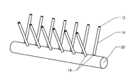
図1に、本発明による、感光性組成物を硬化させるための照明装置10の一実施形態を示す。それは、発光ダイオード12の配列と、対応する導光部16の配列とを有する。それぞれの導光部16は、入光端14及び光出力端18を有する。それぞれの発光ダイオード12が、それが並置された導光部16の入光端14に光を発するために設置されるように、それぞれの発光ダイオード12は、1つの導光部16の入光端14において単一の導光部16と並置されている。その照明装置は、電磁スペクトルの紫外光及び/又は可視光の領域内の光に対して実質的に透明である光学式の集光部20も有する。集光部20は、長さ及び幅、集光部の長さに沿った入光領域22、及び入光領域から間隔を空けた位置に集光部の長さに沿った光出力領域24を有する。それぞれの導光部16の光出力端18は、入光領域22において集光部20にその長さに沿って接する。本発明の目的のために、「接する」の用語は、導光部16の光出力端18が集光部20の入光領域22に接触している、又は導光部16の光出力端18と集光部20の入光領域22とが互いの約0.010インチ以内であることを意味する。
FIG. 1 shows an embodiment of a
次いで、すべての発光ダイオードから集光された光は、光出力領域24に沿って集光部20から出る。本発明の一実施形態において、その照明装置は、発光ダイオード及び導光部の組合せの単一の配列26を有することができる。本発明の別の実施形態において、その照明装置は、配列26に配置された発光ダイオードが、集光部からの第1の距離にあり、配列28の発光ダイオードが、集光部からの第2の距離にあり、第2の距離が第1の距離と異なるように配置された、発光ダイオード及び導光部の組合せの1つより多い配列28を有することができる。好ましい実施形態において、その照明装置は、発光ダイオード近傍に位置する1つ又は複数の放熱装置30をさらに含み、発光ダイオードからの熱を集光部20から熱伝導で取り去ることが可能である。
Next, the light collected from all the light emitting diodes exits the
発光ダイオードは、紫外光、可視光又は両方の1つ又は複数の波長を発することが可能である。一実施形態において、発光ダイオードは、約200nmから約800nmの範囲内の光を発することが可能である。別の実施形態において、発光ダイオードは、約250nmから約450nmの範囲内の光を発することが可能である。 The light emitting diode can emit one or more wavelengths of ultraviolet light, visible light, or both. In one embodiment, the light emitting diode can emit light in the range of about 200 nm to about 800 nm. In another embodiment, the light emitting diode can emit light in the range of about 250 nm to about 450 nm.
図2に、集光部20が実質的に円形の断面を有する、本発明の別の実施形態を示す。この実施形態において、導光部16は湾曲している。図3に、集光部が実質的に長円形の断面を有し、導光部が直線形で互いに等間隔である、本発明の別の実施形態を示す。図4に、集光部が実質的に半円形の断面を有し、導光部が直線形で互いに等間隔である、本発明の別の実施形態を示す。
FIG. 2 shows another embodiment of the present invention in which the
好ましくは、集光部20は、円形、四角形、六角形又は長円形の断面を有する棒を含む。好ましくは、導光部16は、円形、四角形、六角形又は長円形の断面を有する棒を含む。図5に、導光部16の断面が六角形である、本発明の別の実施形態を示す。図6に、導光部16及び集光部20が円形の断面を有し、導光部16が互いに等間隔である、本発明の別の実施形態を示す。図7に示す本発明の別の実施形態において、照明装置1は、電磁スペクトルの紫外光及び/又は可視光の領域内の光に対して実質的に透明である第2の集光部32をさらに含む。第2の集光部32も、長さ及び幅を有する。第2の集光部32は、この長さに沿った入光領域34と、集光部の長さに沿って入光領域から間隔を空けた位置にある光出力領域36とを有する。第2の集光部32の入光領域34が、集光部20の光出力領域22の長さに沿って位置するように、第2の集光部32は設置される。図8に、導光部16が、広い円錐部及び狭い円錐部を有する先細の円錐形の断面を有し、導光部16の光出力端18が、集光部においてそれらの広い円錐部に沿って接している、本発明の別の実施形態を示す。図9に、導光部の光出力端18が、集光部20の中心の位置より集光部20の末端の位置において近い間隔であるように、導光部16の光出力端18が、集光部の入光領域に沿って設置されている、本発明の別の実施形態を示す。好ましくは、集光部の光出力領域に沿った光強度の出力の変化が、光出力領域に沿って約25%未満、より好ましくは5%未満であるように、発光ダイオードが選択され、導光部が集光部の入光領域に沿って設置される。図10に、導光部16の光出力端18が、集光部の入光領域に沿って様々な角度で設置されている、本発明の別の実施形態を示す。図11に、導光部16が様々な高さを有する、本発明の別の実施形態を示す。図12に、導光部16が、放熱器30に隣接して設置されている、本発明の実施形態を示す。
Preferably, the
使用時において、上述の照射装置を用意する。この装置は、基材38上に配置された感光性組成物に隣接して設置される。集光部の光出力領域からの、電磁スペクトルの紫外光及び/又は可視光の領域内の光40を、感光性組成物上に導くことにより、感光性組成物は硬化される。使用時において、上述の導光露光装置10及び感光性組成物は、基材38上に配置される。UV光及び/又は可視光は、導光部16及び集光部20を通して、感光性組成物の状態に変化を引き起こすのに十分な時間、及び十分な光強度で、LED12の配列から感光性組成物上に導かれる。感光性組成物は、適切に、当技術分野において周知である光硬化性接着剤組成物、塗料組成物、カプセル封入剤組成物、マスキング組成物又は密封剤組成物である。感光性組成物には、アクリレート、メタクリレート、シアノアクリレート、エポキシ、又はこれらの組合せを含む、重合性又は架橋性の材料が含まれる。これらは、紫外光もしくは可視光、又は両方に反応性であることができる。選択された基材38上に未硬化の形態の感光性組成物を配置することにより、その導光露光装置はオペレータにより使用される。感光性材料がUV/可視光に露光して、感光性組成物に所望の物理的変化が生じる所定の時間の間、LEDを作動したままにする。
At the time of use, the above-mentioned irradiation apparatus is prepared. This device is placed adjacent to the photosensitive composition disposed on the
感光性組成物は、有機ラジカル重合性成分及び重合開始剤の混合物を含む、実質的に均一な流体を一般に含む。有機ラジカル重合性成分は、少なくとも1つ、好ましくは2つのオレフィン性不飽和二重結合を有するモノマー、オリゴマー又はポリマーであることができる。このようなものは、当技術分野において周知である。有用なラジカル重合性成分には、アクリレート及びメタクリレートが挙げられる。有機ラジカル重合性成分は、十分な化学線放射に曝された際に重合するのに十分な量で存在する。好ましい実施形態において、有機ラジカル重合性成分は、感光性組成物全体の非溶媒部に基づいて約1重量%から約99重量%、好ましくは約50%から約99%の量で感光性組成物全体の中に存在する。ラジカル生成成分は、好ましくは、十分な化学線放射に曝された際に重合性化合物の重合を生じさせるのに十分な量で存在する。重合開始剤は、感光性組成物の非溶媒部の約0.1%から約50%、より好ましくは約0.1%から約10%を構成することができる。 The photosensitive composition generally comprises a substantially uniform fluid comprising a mixture of organic radical polymerizable components and a polymerization initiator. The organic radically polymerizable component can be a monomer, oligomer or polymer having at least one, preferably two olefinically unsaturated double bonds. Such are well known in the art. Useful radical polymerizable components include acrylates and methacrylates. The organic radical polymerizable component is present in an amount sufficient to polymerize when exposed to sufficient actinic radiation. In a preferred embodiment, the organic radical polymerizable component is present in the photosensitive composition in an amount of about 1% to about 99% by weight, preferably about 50% to about 99%, based on the non-solvent portion of the total photosensitive composition. It exists in the whole. The radical generating component is preferably present in an amount sufficient to cause polymerization of the polymerizable compound when exposed to sufficient actinic radiation. The polymerization initiator can comprise from about 0.1% to about 50%, more preferably from about 0.1% to about 10% of the non-solvent portion of the photosensitive composition.
場合による様々な添加剤を、放射硬化性組成物の具体的な最終用途、及び他の様々な条件に応じて組成物に添加することができる。これらの例には、熱重合禁止剤、可塑剤、増量剤、導電性粒子、熱伝導性粒子、スペーサー、着色剤、接着促進剤、界面活性剤、増感剤及び露光指示薬等が挙げられる。感光性組成物は、接着剤又は塗料の組成物としての用途が見出される。 Various optional additives can be added to the composition depending on the specific end use of the radiation curable composition and various other conditions. Examples thereof include thermal polymerization inhibitors, plasticizers, extenders, conductive particles, thermally conductive particles, spacers, colorants, adhesion promoters, surfactants, sensitizers, exposure indicators, and the like. The photosensitive composition finds use as an adhesive or paint composition.
本発明の好ましい実施形態において、感光性組成物は、アクリレートモノマー及び/又はメタクリレートモノマーと組み合わせた、ウレタンのアクリレート及び/もしくはメタクリレートのオリゴマー、ならびに/又はエポキシオリゴマーである重合性成分を有し、重合開始剤は、ケトン及び/又はホスフィンオキシドを含む。感光性組成物は、実質的に均一な流体が形成されるまで、組成物の成分を混合することにより調製され得る。次いで、感光性組成物は、基材上に塗料として塗布され、重合性成分の重合を開始するのに十分な紫外光又は可視光の放射に曝される。露光時間の長さは、当業者により容易に決定でき、放射硬化性組成物に特有の成分の選択に依存する。一般に、露光は、約1秒から約60秒、好ましくは約2秒から約30秒、より好ましくは約2秒から約15秒の範囲である。一般に、露光の強度は、約10mW/cm2から約20mW/cm2、好ましくは約50mW/cm2から約15mW/cm2、より好ましくは約100mW/cm2から約10mW/cm2の範囲である。 In a preferred embodiment of the present invention, the photosensitive composition has a polymerizable component that is an oligomer of urethane acrylate and / or methacrylate and / or an epoxy oligomer in combination with an acrylate monomer and / or a methacrylate monomer, and is polymerized. Initiators include ketones and / or phosphine oxides. The photosensitive composition can be prepared by mixing the components of the composition until a substantially uniform fluid is formed. The photosensitive composition is then applied as a paint on the substrate and exposed to sufficient ultraviolet or visible radiation to initiate polymerization of the polymerizable component. The length of the exposure time can be readily determined by one skilled in the art and depends on the choice of components specific to the radiation curable composition. Generally, the exposure ranges from about 1 second to about 60 seconds, preferably from about 2 seconds to about 30 seconds, more preferably from about 2 seconds to about 15 seconds. Generally, the intensity of exposure is in the range of about 10 mW / cm 2 to about 20 mW / cm 2 , preferably about 50 mW / cm 2 to about 15 mW / cm 2 , more preferably about 100 mW / cm 2 to about 10 mW / cm 2 . is there.
本発明によれば、基材に対して十分な強度の光を均一に照射することができる。本発明は、多種の感光性材料を迅速に硬化させることができ、その応用範囲は広いものとなっている。 According to the present invention, it is possible to uniformly irradiate the substrate with light having sufficient intensity. The present invention can rapidly cure a variety of photosensitive materials and has a wide range of applications.
10 照明装置
12 発光ダイオード
14 入光端
16 導光部
18 光出力端
20 集光部
22 入光領域
24 光出力領域
26 単一の配列
28 1つより多い配列
30 放熱装置(放熱器)
32 第2の集光部
34 入光領域
36 光出力領域
38 基材
40 光
DESCRIPTION OF
32 Second
Claims (7)
電磁スペクトルの紫外光及び/又は可視光の領域内の光に対して実質的に透明である光学式の集光部を含み、前記集光部は、長さ及び幅を有すると共に、集光部の長さに沿った入光領域、及び、集光部の長さに沿って入光領域から間隔を空けた位置にある光出力領域を有し、
それぞれ入光端及び光出力端を有する複数の導光部を含み、前記導光部の光出力端は、集光部の長さに沿って入光領域に接しており、
前記導光部の入光端に並置され、導光部の入光端に光を発することが可能である、複数の発光ダイオードを含む照明装置。 A lighting device for curing a photosensitive composition comprising:
An optical condensing part that is substantially transparent to light in the ultraviolet and / or visible light region of the electromagnetic spectrum, the condensing part having a length and a width; A light incident area along the length of the light output area, and a light output area at a position spaced from the light incident area along the length of the light collecting portion,
Each including a plurality of light guide portions each having a light incident end and a light output end, and the light output end of the light guide portion is in contact with the light incident region along the length of the light collecting portion;
An illumination device including a plurality of light emitting diodes juxtaposed to a light incident end of the light guide unit and capable of emitting light to the light incident end of the light guide unit.
電磁スペクトルの紫外光及び/又は可視光の領域内の光に対して実質的に透明である光学式の集光部を含み、
前記集光部は、長さ及び幅を有すると共に、集光部の長さに沿った入光領域、及び、集光部の長さに沿って入光領域から間隔を空けた位置にある光出力領域を有し、
それぞれ入光端及び光出力端を有する複数の導光部を含み、
前記導光部の光出力端は、集光部の長さに沿って入光領域に接しており、
前記導光部の入光端に並置され、導光部の入光端に光を発することが可能である、複数の発光ダイオードを含む照明装置を用意すること、
ii)基材上に配置された感光性組成物を用意すること、次いで、
iii)電磁スペクトルの紫外光及び/又は可視光の領域内の光を、集光部の光出力領域から感光性組成物に導くことにより、感光性組成物を露光させること、
を含む、感光性組成物の露光方法。 i) a lighting device for curing the photosensitive composition comprising:
An optical concentrator that is substantially transparent to light in the ultraviolet and / or visible region of the electromagnetic spectrum;
The condensing unit has a length and a width, a light incident region along the length of the light condensing unit, and light at a position spaced from the light incident region along the length of the condensing unit. Has an output area,
A plurality of light guides each having a light incident end and a light output end;
The light output end of the light guide part is in contact with the light incident region along the length of the light collecting part,
Providing an illuminating device including a plurality of light emitting diodes, juxtaposed to a light incident end of the light guide, and capable of emitting light to the light incident end of the light guide;
ii) providing a photosensitive composition disposed on a substrate;
iii) exposing the photosensitive composition by directing light in the ultraviolet and / or visible light region of the electromagnetic spectrum from the light output region of the condensing part to the photosensitive composition;
The exposure method of the photosensitive composition containing this.
Applications Claiming Priority (2)
| Application Number | Priority Date | Filing Date | Title |
|---|---|---|---|
| US12/769,594 | 2010-04-28 | ||
| US12/769,594 US8134132B2 (en) | 2010-04-28 | 2010-04-28 | Exposure device having an array of light emitting diodes |
Publications (2)
| Publication Number | Publication Date |
|---|---|
| JP2011233522A true JP2011233522A (en) | 2011-11-17 |
| JP2011233522A5 JP2011233522A5 (en) | 2014-06-19 |
Family
ID=44858454
Family Applications (1)
| Application Number | Title | Priority Date | Filing Date |
|---|---|---|---|
| JP2011098386A Pending JP2011233522A (en) | 2010-04-28 | 2011-04-26 | Exposure device having array of light-emitting diode |
Country Status (5)
| Country | Link |
|---|---|
| US (1) | US8134132B2 (en) |
| EP (1) | EP2400324A1 (en) |
| JP (1) | JP2011233522A (en) |
| KR (1) | KR20110120210A (en) |
| CN (1) | CN102236266A (en) |
Families Citing this family (11)
| Publication number | Priority date | Publication date | Assignee | Title |
|---|---|---|---|---|
| CN102246219B (en) * | 2008-12-09 | 2015-02-25 | 皇家飞利浦电子股份有限公司 | Lighting system with fiber diffusing element |
| US9108369B2 (en) * | 2011-07-25 | 2015-08-18 | Microsoft Technology Licensing, Llc | Wedge light guide |
| US8944659B2 (en) | 2012-02-21 | 2015-02-03 | Apple Inc. | Methods for assembling electronic devices using embedded light guide structures |
| CN103862854A (en) * | 2012-12-14 | 2014-06-18 | 江苏广发光电科技有限公司 | Device for solidifying printing ink |
| ITMI20130155A1 (en) * | 2013-02-05 | 2014-08-06 | Asr R Di Montagnani Valerio | DEVICE FOR HYGIENE OF MEDICAL INSTRUMENTS |
| US10064940B2 (en) | 2013-12-11 | 2018-09-04 | Siva Therapeutics Inc. | Multifunctional radiation delivery apparatus and method |
| US10180248B2 (en) | 2015-09-02 | 2019-01-15 | ProPhotonix Limited | LED lamp with sensing capabilities |
| FR3049686B1 (en) * | 2016-03-29 | 2022-07-01 | Peugeot Citroen Automobiles Sa | LIGHTING DEVICE COMPRISING A HOUSING EQUIPPED WITH A RECEPTION POLE FOR A CYLINDRICAL SECTION OF A LIGHT GUIDE. |
| WO2017174549A1 (en) * | 2016-04-04 | 2017-10-12 | Heraeus Noblelight Gmbh | Method for irradiating treatment goods in industrial processes |
| CN110024144B (en) | 2016-12-01 | 2022-11-25 | 昕诺飞控股有限公司 | Light emitting apparatus |
| EP4127003A1 (en) | 2020-03-31 | 2023-02-08 | Dymax Corporation | Hybrid light-curing composition |
Citations (3)
| Publication number | Priority date | Publication date | Assignee | Title |
|---|---|---|---|---|
| JPH10188647A (en) * | 1996-12-26 | 1998-07-21 | Iwasaki Electric Co Ltd | Ultraviolet curing device |
| JP2002324407A (en) * | 2001-04-24 | 2002-11-08 | Hybec Corp | Method to convert a point light source to a line light source |
| JP2009070817A (en) * | 2007-08-22 | 2009-04-02 | Masaaki Miyamoto | Light-emitting body and illuminating device equipped with it |
Family Cites Families (30)
| Publication number | Priority date | Publication date | Assignee | Title |
|---|---|---|---|---|
| US4677531A (en) * | 1986-01-31 | 1987-06-30 | Applied Intelligent Systems, Inc. | Inspection illumination device |
| US4948214A (en) | 1989-07-10 | 1990-08-14 | Eastman Kodak Company | Step-index light guide and gradient index microlens device for LED imaging |
| US5217290A (en) * | 1991-12-20 | 1993-06-08 | Ford Motor Company | Miniaturized fiberoptic illuminating device |
| US5222794A (en) * | 1991-12-20 | 1993-06-29 | Ford Motor Company | Fiberoptic line-of-light illuminating device |
| FR2732094A1 (en) * | 1995-03-22 | 1996-09-27 | Philips Eclairage | LIGHT GENERATOR FOR OPTICAL FIBERS |
| US5854865A (en) | 1995-12-07 | 1998-12-29 | The United States Of America As Represented By The Secretary Of The Navy | Method and apparatus for side pumping an optical fiber |
| GB2370992B (en) | 2000-03-23 | 2002-11-20 | Photo Therapeutics Ltd | Therapeutic light source and method |
| US6554463B2 (en) | 2000-05-19 | 2003-04-29 | Addent Inc. | Optical waveguide concentrator and illuminating device |
| US6956701B1 (en) * | 2004-04-26 | 2005-10-18 | Infocus Corporation | Method and apparatus for combining light paths of multiple colored light sources through a common integration tunnel |
| US6784603B2 (en) * | 2001-07-20 | 2004-08-31 | Teledyne Lighting And Display Products, Inc. | Fluorescent lighting apparatus |
| US7153015B2 (en) * | 2001-12-31 | 2006-12-26 | Innovations In Optics, Inc. | Led white light optical system |
| DE60337026D1 (en) * | 2002-11-07 | 2011-06-16 | Sony Deutschland Gmbh | LIGHTING ARRANGEMENT FOR A PROJECTION DEVICE |
| US6880954B2 (en) * | 2002-11-08 | 2005-04-19 | Smd Software, Inc. | High intensity photocuring system |
| AU2003297588A1 (en) * | 2002-12-02 | 2004-06-23 | 3M Innovative Properties Company | Illumination system using a plurality of light sources |
| JP3838196B2 (en) | 2002-12-24 | 2006-10-25 | ブラザー工業株式会社 | Electronics |
| KR100779133B1 (en) * | 2003-08-06 | 2007-11-23 | 씨씨에스 가부시키가이샤 | Linear light irradiation device |
| US7250611B2 (en) * | 2003-12-02 | 2007-07-31 | 3M Innovative Properties Company | LED curing apparatus and method |
| JP4300123B2 (en) | 2004-01-13 | 2009-07-22 | スタンレー電気株式会社 | LED lamp using light guide |
| KR101074984B1 (en) * | 2004-03-11 | 2011-10-18 | 톰슨 라이센싱 | Multiple lamp illumination system with polarization recovery and integration |
| JP4020397B2 (en) * | 2004-06-14 | 2007-12-12 | 惠次 飯村 | Surface light source using point light source |
| US7182498B2 (en) * | 2004-06-30 | 2007-02-27 | 3M Innovative Properties Company | Phosphor based illumination system having a plurality of light guides and an interference reflector |
| US7255469B2 (en) * | 2004-06-30 | 2007-08-14 | 3M Innovative Properties Company | Phosphor based illumination system having a light guide and an interference reflector |
| AU2005270014A1 (en) | 2004-07-02 | 2006-02-09 | Discus Dental, Llc. | Curing light having a reflector |
| US8251689B2 (en) | 2005-09-20 | 2012-08-28 | Summit Business Products, Inc. | Ultraviolet light-emitting diode device |
| US7470921B2 (en) | 2005-09-20 | 2008-12-30 | Summit Business Products, Inc. | Light-emitting diode device |
| US7360934B2 (en) * | 2005-10-24 | 2008-04-22 | Sumitomo Electric Industries, Ltd. | Light supply unit, illumination unit, and illumination system |
| CN101542245A (en) | 2006-11-30 | 2009-09-23 | 皇家飞利浦电子股份有限公司 | Illumination system |
| US20080310181A1 (en) * | 2007-06-15 | 2008-12-18 | Microalign Technologies, Inc. | Brightness with reduced optical losses |
| US7959282B2 (en) * | 2007-12-20 | 2011-06-14 | Summit Business Products, Inc. | Concentrated energy source |
| CN102460254B (en) * | 2009-04-29 | 2015-05-06 | Plc诊断股份有限公司 | Waveguide-based detection system with scanning light source |
-
2010
- 2010-04-28 US US12/769,594 patent/US8134132B2/en active Active
-
2011
- 2011-03-29 EP EP11160254A patent/EP2400324A1/en not_active Withdrawn
- 2011-03-30 KR KR1020110028703A patent/KR20110120210A/en not_active Application Discontinuation
- 2011-04-26 JP JP2011098386A patent/JP2011233522A/en active Pending
- 2011-04-28 CN CN2011101171742A patent/CN102236266A/en active Pending
Patent Citations (3)
| Publication number | Priority date | Publication date | Assignee | Title |
|---|---|---|---|---|
| JPH10188647A (en) * | 1996-12-26 | 1998-07-21 | Iwasaki Electric Co Ltd | Ultraviolet curing device |
| JP2002324407A (en) * | 2001-04-24 | 2002-11-08 | Hybec Corp | Method to convert a point light source to a line light source |
| JP2009070817A (en) * | 2007-08-22 | 2009-04-02 | Masaaki Miyamoto | Light-emitting body and illuminating device equipped with it |
Also Published As
| Publication number | Publication date |
|---|---|
| KR20110120210A (en) | 2011-11-03 |
| US20110268888A1 (en) | 2011-11-03 |
| US8134132B2 (en) | 2012-03-13 |
| CN102236266A (en) | 2011-11-09 |
| EP2400324A1 (en) | 2011-12-28 |
Similar Documents
| Publication | Publication Date | Title |
|---|---|---|
| JP2011233522A (en) | Exposure device having array of light-emitting diode | |
| US7202490B2 (en) | LED modifying apparatus and method | |
| US7802910B2 (en) | Light guide exposure device | |
| EP3043740B1 (en) | Thin led film-based curing light system | |
| JP5001937B2 (en) | Solid state light source for curing and surface modification | |
| JP3197099U (en) | Linear Fresnel Optics to reduce the angular spread of light from LED arrays | |
| JP5727682B2 (en) | Waveguide | |
| KR20050044865A (en) | High efficiency solid-state light source and methods of use and manufacture | |
| KR20060121264A (en) | Led modifying apparatus and method | |
| US9388967B2 (en) | Edge weighted spacing of LEDs for improved uniformity range | |
| JP2012505522A (en) | High illumination transmission decentered optical system | |
| TWI615580B (en) | Wrap-around window for lighting module | |
| KR101288390B1 (en) | Lamp with Ultra Violet Light Emitting Diode | |
| JP2012089601A (en) | Light irradiation device | |
| TWM573697U (en) | Light curing resin light source structure |
Legal Events
| Date | Code | Title | Description |
|---|---|---|---|
| A521 | Request for written amendment filed |
Free format text: JAPANESE INTERMEDIATE CODE: A523 Effective date: 20140424 |
|
| A621 | Written request for application examination |
Free format text: JAPANESE INTERMEDIATE CODE: A621 Effective date: 20140424 |
|
| A977 | Report on retrieval |
Free format text: JAPANESE INTERMEDIATE CODE: A971007 Effective date: 20141211 |
|
| A131 | Notification of reasons for refusal |
Free format text: JAPANESE INTERMEDIATE CODE: A131 Effective date: 20141215 |
|
| A02 | Decision of refusal |
Free format text: JAPANESE INTERMEDIATE CODE: A02 Effective date: 20150508 |