JP2018092998A - Circuit board and electronic apparatus - Google Patents
Circuit board and electronic apparatus Download PDFInfo
- Publication number
- JP2018092998A JP2018092998A JP2016233367A JP2016233367A JP2018092998A JP 2018092998 A JP2018092998 A JP 2018092998A JP 2016233367 A JP2016233367 A JP 2016233367A JP 2016233367 A JP2016233367 A JP 2016233367A JP 2018092998 A JP2018092998 A JP 2018092998A
- Authority
- JP
- Japan
- Prior art keywords
- circuit board
- reinforcing member
- component
- reinforcing
- bump
- Prior art date
- Legal status (The legal status is an assumption and is not a legal conclusion. Google has not performed a legal analysis and makes no representation as to the accuracy of the status listed.)
- Granted
Links
Images


Classifications
-
- H—ELECTRICITY
- H01—ELECTRIC ELEMENTS
- H01L—SEMICONDUCTOR DEVICES NOT COVERED BY CLASS H10
- H01L2924/00—Indexing scheme for arrangements or methods for connecting or disconnecting semiconductor or solid-state bodies as covered by H01L24/00
- H01L2924/15—Details of package parts other than the semiconductor or other solid state devices to be connected
- H01L2924/151—Die mounting substrate
- H01L2924/153—Connection portion
- H01L2924/1531—Connection portion the connection portion being formed only on the surface of the substrate opposite to the die mounting surface
- H01L2924/15311—Connection portion the connection portion being formed only on the surface of the substrate opposite to the die mounting surface being a ball array, e.g. BGA
Abstract
Description
本発明の実施形態は、回路基板及び電子機器に関する。 Embodiments described herein relate generally to a circuit board and an electronic device.
回路基板に補強板を取り付けることがある。 A reinforcing plate may be attached to the circuit board.
回路基板には、高い耐衝撃性と薄板化が要望されている。 The circuit board is required to have high impact resistance and thin plate.
本発明の目的は、薄板化と、耐衝撃性の向上を図ることができる回路基板を提供することである。 An object of the present invention is to provide a circuit board capable of reducing the thickness and improving the impact resistance.
実施形態によれば、回路基板は、回路基板本体と、回路基板本体上に取り付けられた電子部品と、回路基板本体上への電子部品の投影領域の内側に設けられ、電子部品と回路基板本体とを電気的に接続させる、回路基板本体上の取付部と、取付部の回路基板本体上の位置に対応して、回路基板本体内部に埋設された補強部材とを備えている。 According to the embodiment, the circuit board is provided inside the circuit board main body, the electronic component attached on the circuit board main body, and the projection area of the electronic component on the circuit board main body. And a reinforcing member embedded in the circuit board body corresponding to the position of the mounting part on the circuit board body.
以下、実施形態の回路基板について、図面を参照して説明する。
(第1実施形態)
第1実施形態の回路基板10は、例えば電子機器としてのノートブック型ポータブルコンピュータ(ノートPC)12に設けられている。図1に示すように、ノートPC12は、第1ユニット14と、第2ユニット16と、ヒンジ部18とを有する。第1ユニット14は、例えば電子機器本体である。第1ユニット14は、第1筐体20を備えている。
Hereinafter, a circuit board according to an embodiment will be described with reference to the drawings.
(First embodiment)
The
図1に示すように、第1筐体20は、上壁21と、底壁23と、周壁(側壁)25とを有している。第1筐体20の周壁25には、少なくとも一つの排気孔27(開口部)が設けられている。第1筐体20は、第1部品34を有する実施形態に係る回路基板10と、ファン40と、ヒートシンク42と、熱伝導部材43(図2参照)とを収容している。熱伝導部材43は、第2部品45に接続している。第2部品45には、従来の補強構造である第2補強部47が設けられている。
As shown in FIG. 1, the
第2ユニット16は、例えば表示部であり、第2筐体22と、この第2筐体22に収容された表示装置24とを備えている。第2筐体22は、表示装置24の表示画面が外部に露出する開口部26を有する。
The
第2筐体22は、ヒンジ部18によって、第1筐体20の後端部に回動可能(開閉可能)に連結されている。これによりノートPC12は、第1ユニット14と第2ユニット16とが重ねられた第1の位置と、第1ユニット14と第2ユニット16とが開かれた第2の位置との間で回動可能である。
The
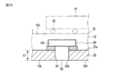
図2、図3に回路基板10を示す。図2は、回路基板10の平面図、図3は、回路基板10を図2の破断線F3−F3で破断して示す断面図である。
The
回路基板10は、平板状で、第1基板30と第2基板32とを有する。第1基板30の上に第2基板32が積層されている。請求項でいう、回路基板本体は、基本的に第1基板30の上に第2基板32が積層された基板である。回路基板10は、第1面10aと、この第1面10aとは反対側に位置した第2面10bとを有する。
The
第1基板30は、第1面30aと、この第1面30aとは反対側に位置した第2面30bとを有する。第2基板32は、第1面32aと、この第1面32aとは反対側に位置した第2面32bとを有する。つまり、回路基板10の第1面10aは、第2基板32の第1面32aであり、回路基板10の第2面10bは、第1基板30の第2面30bである。第1面10aに、第1部品34が実装されている。第2面10bに、上述したように第2部品45が実装され、第2部品45に、熱伝導部材43が設けられている。
The
尚、本実施形態では、回路基板10の第1面10aが第1筐体20の上方に面し、第2面10bが第1筐体20の底壁23に対向しているが、これに代えて、第1面10aが底壁23に対向し、第2面10bが第1筐体20の上壁21に面してもよい。
In the present embodiment, the
第1部品34は、例えば表面実装タイプの半導体部品である。第1部品34は、通電されることで発熱する。第1部品34は、例えば比較的発熱量が小さく、自然放熱で十分な放熱が可能である。第1部品34は、ヒートシンク42に熱接続されていない。
The
図3、図4に示すように、第1部品34は、BGA(Ball Grid Array)である。第1部品34は、パッケージ44と、このパッケージの裏面(下面)に格子状に並べられた複数のバンプ46とを有する。パッケージ44は、基板48と、この基板48に搭載された半導体(電子部品)50とを含む。尚、第1部品34は、BGAに限定されるものではなく、エリアアレイ型またはその他の半導体部品を含む種々の部品が適宜該当する。
As shown in FIGS. 3 and 4, the
図2、図3、図4に示すように、パッケージ44は、例えば四角形状の扁平な箱状に形成されている。パッケージ44は、半導体50や電子部品を外部環境から保護するケースであり、封止部の一例である。尚、パッケージ44は、半導体50や電子部品を完全に覆うものに限られない。第1部品34は、半導体50や電子部品の一部または全部が外部に露出されているものでもよい。
As shown in FIGS. 2, 3, and 4, the
パッケージ44は、第1面44aと、第2面44bと、外周面44dとを有する。第2面44bは、第1面44aとは反対側に位置し、第1面44aと略平行に広がる。第2面44bは、いわゆるパッケージ44の裏面(第1部品の裏面)であり、回路基板10に向かい合う。請求項でいう投影領域は、外周面44dの形状に相当する。
The
第2面44bには、複数のバンプ46が設けられている。外周面44dは、第1面44a及び第2面44bと交差する方向(略直交する方向)に延びている。外周面44dは、第1面44aと第2面44bとに亘り、第1面44aの周縁と第2面44bの周縁とを繋いでいる。
A plurality of
パッケージ44の外周面44dは、四つの角部60と、この四つの角部60の間に延びた四つの側壁62とを有する。四つの角部60は、第1角部60a、第2角部60b、第3角部60c、及び第4角部60dを含む。
The outer
第2角部60bは、第1角部60aに隣り合う。第3角部60cは、第1角部60aの対角に位置する。第4角部60dは、第1角部60aに隣り合うとともに、第2角部60bの対角に位置する。尚、四つの角部60は、図25に示すように、それぞれ丸みを有してもよい。
The second corner 60b is adjacent to the first corner 60a. The third corner portion 60c is located on the opposite side of the first corner portion 60a. The fourth corner portion 60d is adjacent to the first corner portion 60a and is located diagonally to the second corner portion 60b. The four
四つの側壁62は、第1側壁62a、第2側壁62b、第3側壁62c、及び第4側壁62dを含む。第1側壁62aは、第1角部60aと第2角部60bとの間に延びる。第2側壁62bは、第2角部60bと第3角部60cとの間に延びる。第3側壁62cは、第3角部60cと第4角部60dとの間に延びる。第4側壁62dは、第4角部60dと第1角部60aとの間に延びる。
The four
図4に示すように、バンプ46は、パッケージ44の第2面44b(裏面)内に設けられ、第1部品34の側壁62よりも内側に位置する。バンプ46は、外周面44dの四つの側壁62に沿って格子状に並べられている。バンプ46は、第1部品34の中央点P(図4参照)を中心にして点対称に配置されている。
As shown in FIG. 4, the
本明細書では、パッケージ44の中央点Pを基準(基点)として、この中央点Pから遠ざかる側を外側、中央点Pに近づく側を内側と規定する。各バンプ46は、回路基板10の第1面10aに、後述する取付部を介して電気的に接続されている。
In this specification, the center point P of the
バンプ46は、図4に示すように、最外周としての第1周R1(第1列、第1ライン)、この第1周R1よりも内側に位置した第2周R2(第2列、第2ライン)、この第2周R2よりも内側に位置した第3周R3(第3列、第3ライン)、この第3周R3よりも内側に位置した第4周R4(第4列、第4ライン)などに分かれて、複数の枠状(矩形状)のラインに沿って配置されている。尚、図4では、各枠の一部を示す。
As shown in FIG. 4, the
図4に示すように、第1周R1(以下、最外周R1ともいう)に位置したバンプ46は、最外周R1の角に位置する第1バンプ46aと、第1バンプ46a以外の第2バンプ46bとを有する。第1バンプ46aは、パッケージ44の角部60に対応した、いわゆるコーナーバンプである。
As shown in FIG. 4, the
第1バンプ46aは、パッケージ44の角部60に最も近傍に位置する。第1部品34は、四つの第1バンプ46aを、四つの角部60の近傍にそれぞれ分かれて有している。
The
第2バンプ46bは、第1バンプ46aに比べて、パッケージ44の角部60から離れている。第2バンプ46bは、パッケージ44の側壁62に沿って並べられている。
The
次に、本実施形態の回路基板10が有する補強構造について説明する。
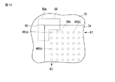
図3、図4に示すように、回路基板10は、回路基板10の内部に補強部36を有している。補強部36は、図3に示すように、回路基板10の第1面10aと第2面10bとの間に埋設されている。補強部36は、パッケージ44の外周面44dに沿う形に形成されている。補強部36は、四つの補強部材66を有している。
Next, a reinforcing structure included in the
As shown in FIGS. 3 and 4, the
補強部材66の1つを図5に示す。補強部材66は、例えば金属プレート(金属片)である。補強部材66は、それぞれ例えば第1部品34の外形に比べて小さなL字形をしている。図4、図5に示すように、補強部材66は、L字状に屈曲した挟み角の外側に位置する第1縁66aと、挟み角の内側に位置する第2縁66bとを有している。第1縁66aは、補強部材66の外縁であり、第2縁66bは、補強部材66の内縁である。
One of the reinforcing
補強部材66の長さLの一例は、約6.0mmである。補強部材66の厚さTの一例は、約0.6mmである。尚、補強部材66の大きさは、これに限定されるものではない。
An example of the length L of the reinforcing
補強部材66は、図4に示すように、第1部品34の四つの角部60にそれぞれに対応して配置されている。補強部材66は、互いに別体であるとともに、第1部品34の四つの角部60に対応して、分かれて設けられている。
As shown in FIG. 4, the reinforcing
四つの補強部材66は、互いの間に隙間Cを有し、それぞれ個別に回路基板10内に設けられている。四つの補強部材66の間の隙間Cは、例えば補強部材66の一辺の長さLよりも大きい。すなわち、補強部材66は、パッケージ44の角部に沿う形に配置されている。
The four reinforcing
図5に示すように、補強部材66は、外縁としての第1縁66a(第1端部)と、内縁としての第2縁66b(第2端部)とを有する。第1縁66aは、最外周R1のバンプ46と、パッケージ44の外周面44d、つまり第1部品34の側壁62との間に位置している。又、内縁である第2縁66bは、最外周R1に位置したバンプ46の内側に位置している。
As shown in FIG. 5, the reinforcing
補強部材66は、例えば第1基板30のパッドにはんだ固定されることで、固定されている。図4に示すように、補強部材66は、最外周の第1周R1に位置したバンプ46と回路基板10の厚み方向に重なる位置に設けられている。
The reinforcing
又、図3、図4に示すように、補強部材66は、第1バンプ46aに対向する位置に設けられているとともに、少なくとも一つの第2バンプ46bには対向していない。すなわち、いくつかの第2バンプ46bの直下には、補強部材66の間に設けられた隙間Cが位置している。
Further, as shown in FIGS. 3 and 4, the reinforcing
図6に、補強部材66を実装する実装工程の一例を示す。図6に示すように、まず、第1基板30の上面の第1面30aに銅箔31を備えた第1基板30を用意する(a)。銅箔31は、回路基板10に取り付けられる第1部品34の取付位置に対応して設けられている。
FIG. 6 shows an example of a mounting process for mounting the reinforcing
第1面30a上の銅箔31にはんだ(はんだペースト)33を印刷する(b)。はんだ33は、回路基板10に取り付けるべき内蔵部品があるときは、その内蔵部品を取り付けるためにも印刷される。
Solder (solder paste) 33 is printed on the
次に、内蔵部品を実装する実装工程で、補強部材66がはんだ33の上にマウントされ、第1リフロー工程を経て、補強部材66が第1基板30の第1面30a上に固定される(c)。その際、回路基板10の内部に埋設される内蔵部品も第1基板30の第1面30aに取り付けられる。すなわち、補強部材66は、回路基板10に内蔵部品を固定させる工程にて第1基板30に固定される。
Next, in the mounting process for mounting the built-in component, the reinforcing
次に、第1基板30の第1面30aの上に第2基板32が設けられる(d)。第2基板32は、補強部材66や内臓部品を覆って第1基板30上に設けられる。第2基板32の第1面32aは、第1基板30の第2面30bと平行に形成される。
Next, the
次に、第2印刷工程で、回路基板10の第1面10a、つまり第2基板32の第1面32aに、はんだ35が印刷される(e)。はんだ35が、請求項でいう取付部に相当する。次に、第1部品34の実装工程で、第1部品34が回路基板10にマウントされ(f)、第2リフロー工程を経ることで、第1部品34が回路基板10の第1面32aに実装される。これにより、回路基板10が完成する(図3参照)。
Next, in the second printing step, the
ここで、補強部材66の材質は、回路基板10と線膨張係数が近い材料であり、例えばステンレス鋼(SUS)である。このため、第2リフロー工程では、回路基板10の熱膨張/収縮に追従して補強部材66が膨張/収縮し、回路基板10に大きなストレスが作用しにくい。
Here, the material of the reinforcing
尚、補強部材66は、上記例に限定されるものではない。補強部材66は、金属でなく、例えば樹脂材料でもよい。また補強部材66は、回路基板10の第1基板30に塗布されて硬化された接着剤やはんだでもよい。
The reinforcing
本実施形態の回路基板10は、回路基板10の第1面10aに実装される、角部60を有する第1部品34と、回路基板10の内部で第1部品34の角部60に対応して設けられた補強部材66とを備えている。
The
補強部材66は、第1部品34の裏面全体に対応したものではなく、最も応力が集中しやすい第1部品34の角部60の近傍を保護する。これにより、回路基板10の剛性をあまり高めることなく、第1部品34の保護を図り、回路基板10の耐衝撃性を高めることができる。
The reinforcing
更に第1部品34は、角部60を有したパッケージ44と、格子状に並べられた複数のバンプ46とを有する。複数のバンプ46のなかで最外周R1に位置したバンプ46は、角部60に位置する第1バンプ46aと、角部60から離れた複数の第2バンプ46bとを含む。そして本実施形態では、補強部材66は、パッケージ44の中心に対して第1バンプ46aよりも外側に位置した第1縁66aを有する。
Further, the
これにより、補強部材66は、回路基板10の端部10d(図2参照)から回路基板10を伝わって第1バンプ46aに向かう応力波を、第1バンプ46aよりも外側で受けることができる。これにより、第1バンプ46aよりも外側に応力集中部をずらすことができる。このため、最も応力が集中しやすかった第1バンプ46aの負荷を減らすことができ、耐衝撃性を高めることができる。
As a result, the reinforcing
又、本実施形態では、四つの補強部材66が設けられている。四つの補強部材66は、互いに別体であるとともに、部品の四つの角部60に分かれて対応している。これにより、第1部品34の四つの角部60が適切に保護され、回路基板10の耐衝撃性を高めることができる。
In the present embodiment, four reinforcing
尚、補強部材66の大きさは、これに限らず、最外周R1に位置したバンプ46だけを覆う小さなものや、最外周R1に位置したバンプ46から第3周R3に位置したバンプまで覆う大きなものでもよい。
The size of the reinforcing
本実施形態では、補強部材66が、回路基板10の内部に埋設されている。これにより、回路基板10は、第1面10aと第2面10bの実装面積を有効に活用することができる。
In the present embodiment, the reinforcing
本実施形態では、最外周のバンプ46は、四つの角部60のなかの一つの角部60の近傍に位置した第1バンプ46aと、この第1バンプ46aに比べて角部60から離れた複数の第2バンプ46bとを含む。補強部材66は、第1バンプ46aに対向するとともに、少なくとも第2バンプ46bの一つに対向していない。これにより、最外周の第1周R1に位置したバンプ46の中でも最も応力が集中しやすい第1バンプ46aの負荷を減らすことができ、耐衝撃性を高めることができる。
In the present embodiment, the outermost
本実施形態では、補強部材66の材料として、回路基板10と線膨張係数が近いステンレス鋼のような部材が使用される。これにより、熱応力による回路基板10への影響を小さく抑えることができる。
In the present embodiment, a member such as stainless steel having a linear expansion coefficient close to that of the
補強部材66が他の内部部品と共に実装工程で実装されるので、バックプレートのようなねじ止め工程や治具が必要なくなる。また、接着剤、テープ、ねじ止めなどのような後工程での作業がなくなる。これらにより、製造コストの低下が図られる。
Since the reinforcing
本実施形態では、補強部材66は、第1部品34の角部60に沿うL字形を有している。補強部材66がL字形であるので、第1部品34の角部60を適切に保護するとともに、補強部材66の材料歩留まりが比較的高くなる。
In the present embodiment, the reinforcing
本実施形態では、補強部材66の第1縁66aは、最外周の第1周R1のバンプ46に沿っている。これにより、最外周R1のバンプ46の負荷を、上記例より更に減らすことができる。
In the present embodiment, the
尚、図9に示すように、補強部材66は、最外周R1に位置したバンプ46に加え、第2周R2のバンプ46に位置するように形成してもよい。更に、補強部材66は、L字形に限られない。図16、図22、図23に示すように、補強部材66は、丸形、四角形、三角形、その他の形状でもよい。
As shown in FIG. 9, the reinforcing
(比較例)
以下、本実施形態に係る回路基板10とその比較例について説明する。
従来、剛性が高い基板の方が部品の保護が図れ、基板の寿命(部品の寿命)が長くなると考えられていた。そのため、回路基板に取り付けられる第1部品に補強板(バックプレート)を設ける場合、補強板は、その第1部品の外形よりも大きくして、補強板で第1部品の全体を覆うようにしていた。
(Comparative example)
Hereinafter, the
Conventionally, it has been considered that a board with higher rigidity can protect a component, and the life of the board (the life of the part) becomes longer. Therefore, when a reinforcing plate (back plate) is provided on the first component attached to the circuit board, the reinforcing plate is made larger than the outer shape of the first component so that the entire first component is covered with the reinforcing plate. It was.
しかしながら、発明者らは、基板に部品の全体を覆うような補強板を取り付けることは、静荷重に対しては有効であるが、振動・衝撃(または熱)に対しては従来考えられているほど有効ではなく、逆に基板の寿命を低下させる可能性があることを見出した。すなわち、本発明者らは、基板の剛性を高めることが、必ずしも部品の保護に繋がらない場合があることを見出した。 However, the inventors attach a reinforcing plate that covers the entire component to the substrate, which is effective for static load, but has been conventionally considered for vibration / impact (or heat). It has been found that it is not as effective and may reduce the life of the substrate. That is, the present inventors have found that increasing the rigidity of the substrate may not necessarily lead to protection of components.
詳しく述べると、本発明者らは、それぞれ同じ部品が実装された2枚の基板の寿命試験を行った。基板は、それぞれ基本的な剛性を有する通常基板と、この通常基板よりも厚く、剛性が高い剛性基板である。これら2枚の通常基板と剛性基板に繰り返し衝撃を加え(例えば落下試験)、それら各基板に不具合が生じるまでの回数をカウントした。上記試験によれば、通常基板に比べて、剛性基板の方が寿命が短くなった。 More specifically, the present inventors conducted a life test on two substrates each mounted with the same component. The substrates are a normal substrate having basic rigidity and a rigid substrate that is thicker and higher in rigidity than the normal substrate. The impact was repeatedly applied to these two normal substrates and rigid substrates (for example, a drop test), and the number of times until each of the substrates was defective was counted. According to the above test, the life of the rigid substrate was shorter than that of the normal substrate.
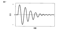
本発明者らは、この理由を次のように分析している。
図7は、剛性が低い回路基板(通常基板)の衝撃入力時の様子を示す。図7、図8の横軸は時間、縦軸は応力である。横軸及び縦軸の値は、図7と図8で同じである。通常基板に衝撃が加わった時、通常基板には所定の振幅で振れる応力が振動として繰り返し作用する。剛性が低い通常基板の場合、応力のピークは高くなるものの、応力が繰り返し作用する回数(図中の波の回数)は少なくなる傾向にある。
The present inventors have analyzed this reason as follows.
FIG. 7 shows a state at the time of impact input of a circuit board (normal board) having low rigidity. 7 and 8, the horizontal axis represents time, and the vertical axis represents stress. The values on the horizontal axis and the vertical axis are the same in FIGS. When an impact is applied to the normal substrate, stress that swings with a predetermined amplitude repeatedly acts as vibration on the normal substrate. In the case of a normal substrate with low rigidity, the stress peak increases, but the number of times the stress repeatedly acts (the number of waves in the figure) tends to decrease.
一方、図8は、剛性が高い剛性基板の衝撃入力時の様子を示す。剛性基板の場合、応力のピークは低くなるものの、応力が繰り返し作用する回数(図中の波の回数)は多くなる傾向にある。寿命に関しては、衝撃入力時に応力が繰り返し作用する回数が重要な要素の一つであり、このため、剛性基板では逆にストレスが作用しやすく、寿命が低下したものと考えられる。 On the other hand, FIG. 8 shows a state at the time of impact input of a rigid substrate having high rigidity. In the case of a rigid substrate, although the stress peak decreases, the number of times stress repeatedly acts (the number of waves in the figure) tends to increase. Regarding the life, the number of times the stress repeatedly acts upon impact input is one of the important factors. For this reason, it is considered that the stress is likely to act on the rigid substrate and the life is reduced.
本実施形態の回路基板10では、補強部材66の取付位置は、第1バンプ46aに対応しているが、少なくとも一つの第2バンプ46bに対応していない。これにより、回路基板10は、壊れやすいところを補強部材66により補強する一方、回路基板10の剛性を低く保つことができている。したがって、本実施形態の回路基板10は、耐衝撃性が向上し、かつ従来のような部品の裏面全体を補強板で覆うような基板に比べて寿命が長くなっている。
In the
次に、回路基板10の第2乃至第12実施形態について説明する。尚、上記第1実施形態の構成と同一または類似の機能を有する構成は、同一の符号を付してその説明に代える。
Next, second to twelfth embodiments of the
(第2実施形態)
図10を参照して、第2実施形態の回路基板10を説明する。回路基板10は、回路基板10の内部に補強部36を有している。補強部36は、4つの補強部材66を備えている。図10は、そのうちの一つの補強部材66を示す。
(Second Embodiment)
With reference to FIG. 10, the
補強部材66は、最外周R1に位置したバンプ46よりも外側に第2縁66bが位置している。すなわち、補強部材66は、回路基板10の厚み方向においてバンプ46に対向していない。このような補強部36によっても、補強部材66は、回路基板10を伝わって回路基板10の端部10d(図2参照)からバンプ46に向かう応力波を、最外周R1に位置したバンプ46よりも外側で受ける。
The reinforcing
これにより、バンプ46にかかる負荷を減らすことができ、回路基板10は、高い耐衝撃性と耐久性が得られる。尚、補強部材66が、最外周R1に位置したバンプ46に対向した位置にある第1実施形態の回路基板10は、この第2実施形態の回路基板10よりも耐衝撃性が高いものと考えられる。
Thereby, the load applied to the
(第3実施形態)
図11を参照して、第3実施形態の回路基板10を説明する。図11に示すように、回路基板10には、パッケージ44の角部60に対応したバンプ46が複数設けられている。バンプ46は、パッケージ44の角部60に対して斜め45度の角度に並べられている。第3実施形態では、補強部材66は、パッケージ44の角部60に対して斜め45度に並べられているバンプ46に沿って、外縁66cがバンプ46と平行に配置されている。更に、補強部材66の外縁66cは、バンプ46の外側に位置している。この構成によっても、回路基板10は、高い耐衝撃性と耐久性が得られる。
(Third embodiment)
With reference to FIG. 11, the
(第4実施形態)
図12を参照して、第4実施形態に係る回路基板10を説明する。本実施形態の回路基板10は、補強部36が第1部品34の外形全体、つまり側壁62に沿って設けられている。補強部36は、第1部品34の四つの側壁62のそれぞれ略中心に対応した位置でスリット80が形成され、四つの補強部材66に互いに別体に分割されている。
(Fourth embodiment)
A
この実施形態によれば、補強部36は、四つの補強部材66に、スリット80により互いに分断されているため、一つの大きな補強部材に比べて全体の剛性は小さい。このため、回路基板10の剛性が高まることを抑制しつつ、バンプ46にかかる負荷の低減を図ることができる。これにより、回路基板10は、高い耐衝撃性と耐久性が得られる。
According to this embodiment, since the reinforcing
(第5実施形態)
次に、図13を参照して、第5実施形態に係る回路基板10を説明する。本実施形態の回路基板10は、補強部材66の第1縁66aが第1部品34の外側、つまり側壁62の外側に位置している。本実施形態の構成によれば、第1実施形態と同様に、回路基板10は、高い耐衝撃性と耐久性が得られる。
(Fifth embodiment)
Next, a
(第6実施形態)
次に、図14を参照して、第6実施形態に係る回路基板10を説明する。本実施形態の回路基板10は、補強部36が第1部品34の全周の一部に設けられている。補強部材66は、第1部品34の四つの側壁62のうちの三つの側壁62に対応して設けられている。
(Sixth embodiment)
Next, a
本実施形態によれば、補強部36が設けられている側の耐衝撃性が向上する。例えば、衝撃が発生する個所が特定できるときは、発生する個所側にのみ補強部材66を設けることで、耐衝撃性を確保し、他の部分に補強部材を設けないことで、剛性を緩和させ、回路基板10の耐久性を向上できる。図14においては、例えば図の右方から衝撃が伝播されてくるものとする。尚、補強部材66は、第1部品34の一つの側壁62、または二つの側壁62に対応して設けられてもよい。
According to this embodiment, the impact resistance on the side where the reinforcing
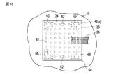
(第7実施形態)
次に、図15を参照して、第7実施形態に係る回路基板10を説明する。本実施形態の回路基板10は、複数設けられた補強部材66の間に、他の内蔵部品(電子部品)82や配線パターン84が配置されている。すなわち、内蔵部品82や配線パターン84は、補強部材66の間の隙間Cに設けられている。内蔵部品82は、例えばコンデンサや抵抗のようなチップ部品である。尚、内蔵部品82は、上記例に限定されるものではない。
(Seventh embodiment)
Next, the
本実施形態によれば、第1実施形態と同様に、回路基板10は、高い耐衝撃性と耐久性が得られる。更に、補強部材66の間の隙間Cを利用して、他の内蔵部品82や配線パターン84が設けられている。これにより、本実施形態では、回路基板10の高密度実装を実現できる。
According to the present embodiment, as in the first embodiment, the
(第8実施形態)
次に、図16を参照して、第8実施形態に係る回路基板10を説明する。本実施形態では、補強部材66の外縁である2つの第1縁66aの交差部(角部)66dは、丸みを有している。回路基板10は、第1部品34の角部60に隣接した領域に内蔵部品(電子部品)82を有する。尚、内蔵部品82は、第1部品34の角部60の近傍に位置し、第1縁66aの交差部(角部)66dに向かい合う。内蔵部品82の一例は、コンデンサや抵抗のようなチップ部品である。尚、内蔵部品82は、上記例に限定されるものではない。
(Eighth embodiment)
Next, a
本実施形態では、補強部材66の外縁の角部66dに丸みが設けられている。これによれば、外側から補強部材66の角部66dに入力される応力を分散させ、角部66dでの応力集中を緩和することができる。本実施形態によれば、第1実施形態と同様に、回路基板10は、高い耐衝撃性と耐久性が得られる。
In this embodiment, the
更に本実施形態によれば、補強部材66の角部66dに隣接した領域を利用し、内蔵部品82が実装されている。補強部材66の角部66dが丸みを有することで、内蔵部品82を補強部材66の近くに配置することができる。これは、回路基板10の高密度実装に寄与する。
Furthermore, according to the present embodiment, the built-in
(第9実施形態)
次に、図17を参照して、第9実施形態の回路基板10を説明する。本実施形態の回路基板10の補強部材66は、例えば金属のような熱伝導性が良好な材料で形成されている。補強部材66は、図17に示すように、突起(フィン)86を有している。突起86は、例えば回路基板10の厚さ方向に延び、突起86の放熱面積を拡大させている。
(Ninth embodiment)
Next, with reference to FIG. 17, the
補強部材66は、回路基板10を介して第1部品34のバンプ46に熱的に接続されており、第1部品34のバンプ46から熱を受けとる。受け取った熱は、突起86から回路基板10の内部に放散される。補強部材66は、第1部品34の放熱を促進する放熱部の一例として機能する。
The reinforcing
本実施形態によれば、第1実施形態と同様に、回路基板10は、高い耐衝撃性と耐久性が得られる。更に本実施形態によれば、突起86を有した補強部材66により、第1部品34の放熱が促進される。これにより、回路基板10の放熱性能の向上も図ることができる。
According to the present embodiment, as in the first embodiment, the
尚、突起86は、補強部材66とは別部材で形成されてもよい。突起86は、何かを支持する支持部でもよく、何かを固定する固定部でもよく、または放熱だけを目的としたものでもよい。突起86は、回路基板10の第2面10bから突出していてもよい。この場合、第1部品34から受けた熱は、第2面10bに露出した突起86から回路基板10の外部に容易に放散される。
The
又、本実施形態では、補強部材66は、回路基板10に設けた孔87の内部に突起86が挿入埋設されている。これにより、補強部材66は、はんだによる固定を行わなくともよくなり、補強部材66を回路基板10に取り付ける取付作業が容易になる。
In the present embodiment, the reinforcing
(第10実施形態)
次に、図18を参照して、第10実施形態に係る回路基板10を説明する。本実施形態の回路基板10の補強部材66は、第1部品34の中央点Pを中心に設けられている。補強部材66は、例えば金属のような熱伝導性が良好な材料で形成されている。補強部材66は、第1部品34のバンプ46に熱的に接続されている。補強部材66は、第1部品34の放熱を促進する放熱部の一例として機能する。
(10th Embodiment)
Next, the
本実施形態によれば、回路基板10は、耐衝撃性が高められる。更に本実施形態によれば、第1部品34の放熱が促進される。尚、補強部材66は、第9実施形態と同様、突起を有していてもよい。
According to this embodiment, the
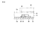
(第11実施形態)
次に、図19を参照して、第11実施形態の回路基板10を説明する。図19は、回路基板10から第2基板32を除いた状態で、補強部材66を上方から示す平面図である。図19に示すように、回路基板10の第1基板30の第1面30aに、補強部材66と銅箔部材88が設けられている。補強部材66は、第1実施形態における補強部材66とほぼ同一の構成である。
(Eleventh embodiment)
Next, with reference to FIG. 19, the
銅箔部材88は、L字状の形状を有している。銅箔部材88は、回路基板10の第1基板30に設けられている。銅箔部材88は、一対互いに平行に、それぞれの間に補強部材66の横幅のスペースをあけて設けられている。
The
補強部材66は、2つの銅箔部材88の間に配置されている。補強部材66は、銅箔部材88の間に配置されると、図20に示すように銅箔部材88により補強部材66の両側が保持される。図20は、図19のF20−F20線で破断した状態を示す断面図である。回路基板10に取り付けるべき内蔵部品があるときは、これと同時に第1基板30に設ける。
The reinforcing
補強部材66が回路基板10の第1基板30上に銅箔部材88により保持されたら、第2基板32を第1基板30の上に形成する。補強部材66は、第1基板30と第2基板32の間、つまり回路基板10の内部に埋設される。これと同時に内蔵部品が、回路基板10に埋設される。補強部材66は、回路基板10に内蔵部品を埋設させる埋設工程により埋設される。第2基板32の第1面32aは、第1基板30の第2面30bと平行に形成される。
When the reinforcing
第2基板32の上面の第1面32aにはんだ(はんだペースト)を印刷する。はんだは、回路基板10に取り付けられる第1部品34の取付位置に対応して印刷される。第1部品34の実装工程で、第1部品34が回路基板10にマウントされ、第2リフロー工程を経ることで、第1部品34が図20に示すように、回路基板10の第1面10aに実装される。補強部材66は、第1部品34のバンプ46の直下に位置している。これにより、回路基板10が完成する。
Solder (solder paste) is printed on the
本実施形態によれば、補強部材66が銅箔部材88の間に配置して保持されるので、補強部材66を組み付ける組付作業が容易となる。
According to this embodiment, since the reinforcing
(第12実施形態)
次に、図21を参照して、第12実施形態の回路基板10を説明する。補強部材66は、円形の頭部90と軸部92とを有する。頭部90は、円板状である。軸部92は、円筒状で、頭部90の平面視の中心に同軸に設けられている。軸部92は、第1基板30に形成された孔94に挿入されている。
(Twelfth embodiment)
Next, with reference to FIG. 21, the
軸部92は、図22に示すように、第1基板30の厚みd1に対応した長さを有している。補強部材66を第1基板30に形成された孔94に組み付けると、軸部92の端面92bが第1基板30の第2面30bとほぼ同一面を形成する。図22は、図21のF22−F22線で破断した状態を示す断面図である。
As shown in FIG. 22, the
本実施形態によれば、補強部材66をはんだによって固定しなくとも第1基板30に固定されるので、補強部材66を回路基板10に取り付ける取付作業が容易になる。第1部品34で発生した熱が、頭部90に吸収され、軸部92を介して回路基板10の外部に放散されるので、第1部品34をより効率よく冷却できる。
According to the present embodiment, since the reinforcing
又、本実施形態によれば、補強部材66の頭部90が円形であるので、応力の分散が緩やかになる。
In addition, according to the present embodiment, since the
(第13実施形態)
次に、図23を参照して、第13実施形態の回路基板10を説明する。本実施形態の回路基板10は、補強部材66の平面視での形状が円形である。補強部材66は、第1実施形態と同様、第1部品34の角部60のバンプ46aに対応する位置にそれぞれ設けられている。補強部材66をこのような形状に形成しても、第1実施形態の回路基板10と同様の効果が得られる。更に、補強部材66が平面視で円形であるので、回路基板10から第1部品34に加えられる応力の分散が緩やかとなる。
(13th Embodiment)
Next, with reference to FIG. 23, the
(第14実施形態)
次に、図24を参照して、第14実施形態の回路基板10を説明する。本実施形態の回路基板10は、補強部材66の平面視での形状が三角形である。補強部材66は、第1実施形態と同様、第1部品34の角部60に対応する位置に設けられている。補強部材66をこのような形状に形成しても、第1実施形態と同様の効果が得られる。更に、補強部材66が平面視で三角形であるので、補強部材66によって補強される個所を限定でき、回路基板10の必要な個所を選択的に補強することができる。
(14th Embodiment)
Next, the
(第15実施形態)
次に、図25を参照して、第15実施形態の回路基板を説明する。本実施形態の回路基板10は、他の部品としての複数の第2部品45と、複数の第2補強部47とを有する。回路基板10の第1面10aや第2面10bに、他の部品としての第2部品45が実装されている。第2部品45が設けられている反対側の面(第2面10bや第1面10a)には、第2部品45に対応した位置にそれぞれ第2補強部47が設けられている。
(Fifteenth embodiment)
Next, a circuit board according to a fifteenth embodiment will be described with reference to FIG. The
第2部品45及び第2補強部47は、回路基板10の端部10dと第1部品34との間に位置する。複数の第2部品45及び第2補強部47は、第1部品34を間に挟むように、第1部品34の両側(または周囲)に配置されている。換言すれば、複数の第2部品45及び第2補強部47によって囲まれた領域に、第1部品34及び補強部36が設けられている。なお、第2部品45及び第2補強部47の数は、それぞれ2つでもよく、3つ以上でもよい。
The
本実施形態の回路基板10によれば、第1実施形態と同様に、第1部品34における耐衝撃性を補強部36により高めることができる。更に、本実施形態では、回路基板10は、第1部品34と回路基板10の端部10dとの間で、第1面10aまたは第2面10bに設けられた第2部品45と、この第2部品45の裏側に設けられ、第2部品45の全周を覆う第2補強部47とが設けられている。
According to the
これによれば、外部からの衝撃を受けやすい回路基板10の端部10d近くが、剛性が高い第2補強部47で補強されるとともに、第1部品34を第2補強部47によって囲み、回路基板10の端部10dから入力される外部衝撃が第1部品34に伝わりにくくなっている。
According to this, the vicinity of the
これにより、回路基板10は、回路基板10の全体としてそれほど剛性を高めずに、外部からの衝撃を直接受けにくい回路基板10の中央部近傍の必要な第1部品34を十分に補強することができる。
As a result, the
上記第1乃至第15実施形態は、それぞれ、ノートPC12の他、テレビジョン受像機、携帯電話、スマートフォン、電子書籍端末、ゲーム機などを含む種々の電子機器に広く適用可能である。
Each of the first to fifteenth embodiments can be widely applied to various electronic devices including a
尚、本発明は上記実施形態そのままに限定されるものではなく、実施段階ではその要旨を逸脱しない範囲で構成要素を変形して具現化できる。また、上記実施形態に開示されている複数の構成要素の適宜な組み合わせにより種々の発明を形成できる。例えば、実施形態に示される全構成要素から幾つかの構成要素を削除してもよい。更に、異なる実施形態に亘る構成要素を適宜組み合わせてもよい。 Note that the present invention is not limited to the above-described embodiment as it is, and can be embodied by modifying the constituent elements without departing from the scope of the invention in the implementation stage. In addition, various inventions can be formed by appropriately combining a plurality of components disclosed in the embodiment. For example, some components may be deleted from all the components shown in the embodiment. Furthermore, you may combine the component covering different embodiment suitably.
P…中央点、R1…第1周、R2…第2周、R3…第3周、R4…第4周、C…隙間、10…回路基板、10a…第1面、10b…第2面、10d…端部、12…ノートPC、14…第1ユニット、16…第2ユニット、18…ヒンジ部、20…第1筐体、21…上壁、22…第2筐体、23…底壁、24…表示装置、25…周壁、26…開口部、27…排気孔、30…第1基板、30a…第1面、30b…第2面、31…銅箔、32…第2基板、32a…第1面、32b…第2面、33、35…はんだ、34…第1部品、36…補強部、40…ファン、42…ヒートシンク、43…ヒートパイプ、44…パッケージ、44a…第1面、44b…第2面、44d…外周面、45…第2部品、46…バンプ、46a…第1バンプ、46b…第2バンプ、48…基板、50…半導体、60…角部、60a…第1角部、60b…第2角部、60c…第3角部、60d…第4角部、62…側壁、62a…第1側壁、62b…第2側壁、62c…第3側壁、62d…第4側壁、66…補強部材、66a…第1縁、66b…第2縁、66c…外縁、66d…角部、80…スリット、82…内蔵部品、84…配線パターン、86…突起、87…孔、88…銅箔部材、90…頭部、92…軸部、94…孔。
P ... center point, R1 ... first turn, R2 ... second turn, R3 ... third turn, R4 ... fourth turn, C ... gap, 10 ... circuit board, 10a ... first face, 10b ... second face, 10d ... end, 12 ... notebook PC, 14 ... first unit, 16 ... second unit, 18 ... hinge part, 20 ... first housing, 21 ... top wall, 22 ... second housing, 23 ... bottom wall , 24 ... display device, 25 ... peripheral wall, 26 ... opening, 27 ... exhaust hole, 30 ... first substrate, 30a ... first surface, 30b ... second surface, 31 ... copper foil, 32 ... second substrate, 32a ... 1st surface, 32b ... 2nd surface, 33, 35 ... Solder, 34 ... 1st part, 36 ... Reinforcement part, 40 ... Fan, 42 ... Heat sink, 43 ... Heat pipe, 44 ... Package, 44a ...
Claims (11)
前記回路基板本体上に取り付けられた電子部品と、
前記回路基板本体上への前記電子部品の投影領域の内側に設けられ、前記電子部品と前記回路基板本体とを電気的に接続させる、前記回路基板本体上の取付部と、
前記取付部の前記回路基板本体上の位置に対応して、前記回路基板本体内部に埋設された補強部と、を備えた回路基板。 A circuit board body;
Electronic components mounted on the circuit board body;
A mounting portion on the circuit board body, which is provided inside a projection region of the electronic component on the circuit board body, and electrically connects the electronic component and the circuit board body;
A circuit board comprising: a reinforcing part embedded in the circuit board main body corresponding to a position of the mounting part on the circuit board main body.
前記補強部は、前記バンプの位置に対応して埋設された補強部材から形成されている請求項1に記載の回路基板。 The electronic component includes a plurality of bumps arranged in a grid, which is electrically connected to the mounting portion.
The circuit board according to claim 1, wherein the reinforcing portion is formed of a reinforcing member embedded corresponding to the position of the bump.
前記補強部材は、第1基板と前記第2基板の間に設けられている請求項4に記載の回路基板。 The circuit board body includes a first substrate and a second substrate stacked on the first substrate,
The circuit board according to claim 4, wherein the reinforcing member is provided between the first board and the second board.
Priority Applications (1)
| Application Number | Priority Date | Filing Date | Title |
|---|---|---|---|
| JP2016233367A JP6855226B2 (en) | 2016-11-30 | 2016-11-30 | Circuit boards and electronic devices |
Applications Claiming Priority (1)
| Application Number | Priority Date | Filing Date | Title |
|---|---|---|---|
| JP2016233367A JP6855226B2 (en) | 2016-11-30 | 2016-11-30 | Circuit boards and electronic devices |
Publications (3)
| Publication Number | Publication Date |
|---|---|
| JP2018092998A true JP2018092998A (en) | 2018-06-14 |
| JP2018092998A5 JP2018092998A5 (en) | 2019-12-26 |
| JP6855226B2 JP6855226B2 (en) | 2021-04-07 |
Family
ID=62566406
Family Applications (1)
| Application Number | Title | Priority Date | Filing Date |
|---|---|---|---|
| JP2016233367A Active JP6855226B2 (en) | 2016-11-30 | 2016-11-30 | Circuit boards and electronic devices |
Country Status (1)
| Country | Link |
|---|---|
| JP (1) | JP6855226B2 (en) |
Citations (6)
| Publication number | Priority date | Publication date | Assignee | Title |
|---|---|---|---|---|
| JP2000068328A (en) * | 1998-08-21 | 2000-03-03 | Olympus Optical Co Ltd | Wiring board for flip-chip mounting |
| JP2011210755A (en) * | 2010-03-29 | 2011-10-20 | Panasonic Corp | Mounting substrate |
| CN102281715A (en) * | 2010-06-10 | 2011-12-14 | 富士通株式会社 | Board reinforcing structure, board assembly, and electronic device |
| US20130016289A1 (en) * | 2011-07-14 | 2013-01-17 | Kabushiki Kaisha Toshiba | Television and electronic apparatus |
| JP2013084748A (en) * | 2011-10-07 | 2013-05-09 | Murata Mfg Co Ltd | Electronic component |
| JP2014130865A (en) * | 2012-12-28 | 2014-07-10 | Keihin Corp | Multilayer circuit board and electronic apparatus having the same |
-
2016
- 2016-11-30 JP JP2016233367A patent/JP6855226B2/en active Active
Patent Citations (9)
| Publication number | Priority date | Publication date | Assignee | Title |
|---|---|---|---|---|
| JP2000068328A (en) * | 1998-08-21 | 2000-03-03 | Olympus Optical Co Ltd | Wiring board for flip-chip mounting |
| JP2011210755A (en) * | 2010-03-29 | 2011-10-20 | Panasonic Corp | Mounting substrate |
| CN102281715A (en) * | 2010-06-10 | 2011-12-14 | 富士通株式会社 | Board reinforcing structure, board assembly, and electronic device |
| US20110303441A1 (en) * | 2010-06-10 | 2011-12-15 | Fujitsu Limited | Board reinforcing structure, board assembly, and electronic device |
| JP2011258836A (en) * | 2010-06-10 | 2011-12-22 | Fujitsu Ltd | Board reinforcing structure, board assembly, and electronic equipment |
| US20130016289A1 (en) * | 2011-07-14 | 2013-01-17 | Kabushiki Kaisha Toshiba | Television and electronic apparatus |
| JP2013026633A (en) * | 2011-07-14 | 2013-02-04 | Toshiba Corp | Television receiver and electronic apparatus |
| JP2013084748A (en) * | 2011-10-07 | 2013-05-09 | Murata Mfg Co Ltd | Electronic component |
| JP2014130865A (en) * | 2012-12-28 | 2014-07-10 | Keihin Corp | Multilayer circuit board and electronic apparatus having the same |
Also Published As
| Publication number | Publication date |
|---|---|
| JP6855226B2 (en) | 2021-04-07 |
Similar Documents
| Publication | Publication Date | Title |
|---|---|---|
| JP5132801B1 (en) | Television receiver and electronic device | |
| JP5445340B2 (en) | Substrate reinforcement structure, substrate assembly, and electronic device | |
| JPWO2006080048A1 (en) | Semiconductor device | |
| JP2000151083A (en) | Enforcing structure for ic package | |
| JP2010278133A (en) | Circuit board | |
| US9451699B2 (en) | Circuit board, electronic device, and method of manufacturing circuit board | |
| US9391029B2 (en) | Electronic device | |
| JP5895091B1 (en) | Optical module | |
| JP2010056489A (en) | Electronic control device | |
| JP6855226B2 (en) | Circuit boards and electronic devices | |
| JP5300994B2 (en) | Electronics | |
| JP2017162860A (en) | Electronic control device | |
| US20130194516A1 (en) | Television and electronic apparatus | |
| US9538661B2 (en) | Electronic device module including a printed circuit | |
| JP4871676B2 (en) | Electronic circuit equipment | |
| JP5617011B2 (en) | Electronic control unit | |
| JP2006229447A (en) | Television reception tuner | |
| JP5300995B2 (en) | Electronics | |
| US20090314536A1 (en) | Printed circuit board, electric instrument, and semiconductor package | |
| JP5290367B2 (en) | Electronic control unit | |
| JP2010093310A (en) | Electronic apparatus | |
| JP2012253214A (en) | Circuit board | |
| JP2018170371A (en) | Electronic apparatus | |
| JP6322764B2 (en) | Circuit board mounting structure and circuit board mounting method | |
| JP4479598B2 (en) | Circuit board mounting structure |
Legal Events
| Date | Code | Title | Description |
|---|---|---|---|
| A711 | Notification of change in applicant |
Free format text: JAPANESE INTERMEDIATE CODE: A711 Effective date: 20181207 |
|
| A521 | Request for written amendment filed |
Free format text: JAPANESE INTERMEDIATE CODE: A523 Effective date: 20191113 |
|
| A621 | Written request for application examination |
Free format text: JAPANESE INTERMEDIATE CODE: A621 Effective date: 20191113 |
|
| A977 | Report on retrieval |
Free format text: JAPANESE INTERMEDIATE CODE: A971007 Effective date: 20200910 |
|
| A131 | Notification of reasons for refusal |
Free format text: JAPANESE INTERMEDIATE CODE: A131 Effective date: 20201020 |
|
| A521 | Request for written amendment filed |
Free format text: JAPANESE INTERMEDIATE CODE: A523 Effective date: 20201130 |
|
| A131 | Notification of reasons for refusal |
Free format text: JAPANESE INTERMEDIATE CODE: A131 Effective date: 20201215 |
|
| A521 | Request for written amendment filed |
Free format text: JAPANESE INTERMEDIATE CODE: A523 Effective date: 20210204 |
|
| TRDD | Decision of grant or rejection written | ||
| A01 | Written decision to grant a patent or to grant a registration (utility model) |
Free format text: JAPANESE INTERMEDIATE CODE: A01 Effective date: 20210224 |
|
| A61 | First payment of annual fees (during grant procedure) |
Free format text: JAPANESE INTERMEDIATE CODE: A61 Effective date: 20210317 |
|
| R150 | Certificate of patent or registration of utility model |
Ref document number: 6855226 Country of ref document: JP Free format text: JAPANESE INTERMEDIATE CODE: R150 |