JP2018026331A5 - - Google Patents
Download PDFInfo
- Publication number
- JP2018026331A5 JP2018026331A5 JP2017137656A JP2017137656A JP2018026331A5 JP 2018026331 A5 JP2018026331 A5 JP 2018026331A5 JP 2017137656 A JP2017137656 A JP 2017137656A JP 2017137656 A JP2017137656 A JP 2017137656A JP 2018026331 A5 JP2018026331 A5 JP 2018026331A5
- Authority
- JP
- Japan
- Prior art keywords
- generator
- signal
- impedance matching
- matching circuit
- measurement
- Prior art date
- Legal status (The legal status is an assumption and is not a legal conclusion. Google has not performed a legal analysis and makes no representation as to the accuracy of the status listed.)
- Granted
Links
- 238000005259 measurement Methods 0.000 claims description 25
- 230000000051 modifying Effects 0.000 claims description 12
- 238000000034 method Methods 0.000 claims description 6
- 239000000758 substrate Substances 0.000 claims 6
- 238000009832 plasma treatment Methods 0.000 claims 1
- 210000002381 Plasma Anatomy 0.000 description 4
- 230000005540 biological transmission Effects 0.000 description 3
- 238000010586 diagram Methods 0.000 description 2
- 230000004907 flux Effects 0.000 description 2
- 150000002500 ions Chemical class 0.000 description 2
- 235000019800 disodium phosphate Nutrition 0.000 description 1
- 239000007789 gas Substances 0.000 description 1
Images
Description
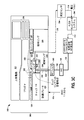
電力量を受信すると、xMHzRF発生器またはx1kHzRF発生器は、その電力量を有するRF信号を生成し、RFケーブル126を介してIMC108へ供給する。IMC108は、IMC108に接続された負荷のインピーダンスとIMC108に接続されたソースのインピーダンスとを整合して、xMHzRF発生器またはx1kHzRF発生器から受信したRF信号から変調RF信号を生成する。変調RF信号は、RFフィルタ208、RFフィルタ208に接続された供給リング、および、同軸ケーブル220を介して、電極202に供給される。電極202とエッジリング110の下面との間のキャパシタンスは、エッジ領域102内のプラズマのインピーダンスを変化させて、さらに、エッジ領域102内のイオン束の方向を変えるために、電極202が変調RF信号を受信した時に変化する。
Upon receiving the amount of power, the xMHz RF generator or x1 kHz RF generator generates an RF signal having that amount of power and supplies it to the
DCバイアスセンサ352の一部は、エッジリング110の開口部を通してエッジリング110内に伸びており、DCバイアスセンサ352の残りの部分は、絶縁リング228の開口部を通して絶縁リング228内に伸びている。DCバイアスセンサ352は、ケーブル356を介して測定センサ354へ接続されている。測定センサ354は、エッジリング110のRF電力によって生成されたDCバイアス(例えば、DCバイアス電圧など)の測定値を提供する。エッジリング110のRF電力は、エッジ領域102内のプラズマのRF電力に基づく。測定センサ354は、転送ケーブル310を介してホストコンピュータシステム306に接続されている。
A portion of the
電力量を受信すると、xMHzRF発生器またはx1kHzRF発生器は、その電力量を有するRF信号を生成し、RFケーブル126を介してIMC108へ供給する。IMC108は、IMC108に接続された負荷のインピーダンスとIMC108に接続されたソースのインピーダンスとを整合して、xMHzRF発生器またはx1kHzRF発生器から受信したRF信号から変調RF信号を生成する。変調RF信号は、RFフィルタ208、RFフィルタ208に接続された供給リング、および、同軸ケーブル220を介して、電極202に供給される。電極202とエッジ領域102との間のキャパシタンスは、エッジ領域102内のプラズマのインピーダンスを変化させて、さらに、エッジ領域102内のイオン束の方向を変えるために、電極202が変調RF信号を受信した時に変化する。
Upon receiving the amount of power, the xMHz RF generator or x1 kHz RF generator generates an RF signal having that amount of power and supplies it to the
RF発生器1002およびマスタRF発生器1014は、RF信号を生成する。マスタRF発生器1014によって生成されるRF信号は、マスタRF発生器1014の動作周波数から予め定められた限度内にある(例えば、同じである、予め格納された限度内にある、など)周波数を有する。マスタRF発生器1014によって生成されたRF信号は、RFケーブル1036および入力1040を介してIMC108へ供給される。同様に、RF発生器1002によって生成されたRF信号は、RFケーブル1034および入力1038を介してIMC108へ供給される。IMC108は、IMC108の出力1008に接続された負荷(例えば、伝送線路124およびチャック114など)のインピーダンスを、IMC108の入力1034および1036に接続されたソース(例えば、RFケーブル1034および1036、ならびに、RF発生器1002および1014など)のインピーダンスと整合して、変調RF信号を生成する。変調RF信号は、プラズマチャンバ104(図1)内でプラズマを生成または維持するために、処理ガスの内の1または複数と共に、RF伝送線路124を介してチャック114へ供給する。
The RF generator 1002 and the master RF generator 1014 generate an RF signal. The RF signal generated by the master RF generator 1014 has a frequency that is within a predetermined limit from the operating frequency of the master RF generator 1014 (eg, is the same, is within a pre-stored limit, etc.). Have. The RF signal generated by master RF generator 1014 is provided to IMC 108 via RF cable 1036 and input 1040. Similarly, the RF signal generated by RF generator 1002 is provided to IMC 108 via RF cable 1034 and input 1038. The
さらに、RF伝送線路122を介して送られる変調RF信号が、スレーブRF発生器1012Bによって生成された状態S2に対する予め定められた範囲内の周波数を有するRF信号に基づいて生成されると、DSP1114は、状態S2に対して、転送ケーブル1030を介して出力1008に関連する状態S2に対する変数を受信し、転送ケーブル1032を介して出力1010に関連する状態S2に対する変数を受信する。出力1008に関連する状態S2に対する変数は、出力1008に関連する変数の位相を含み、出力1010に関連する状態S2に対する変数は、出力1008に関連する変数の位相を含む。一例として、状態S2に対する出力1008に関連する変数の位相は、状態S1に対する出力1008に関連する変数の位相とは異なる(例えば、より小さい、より大きい、など)。別の例として、状態S2に対する出力1008に関連する変数の位相は、状態S1に対する出力1008に関連する変数の位相と同じである。一例として、状態S2に対する出力1010に関連する変数の位相は、状態S1に対する出力1010に関連する変数の位相とは異なる(例えば、より小さい、より大きい、など)。別の例として、状態S2に対する出力1010に関連する変数の位相は、状態S1に対する出力1010に関連する変数の位相と同じである。
Further, when the modulated RF signal sent via the
図14は、マスタRF発生器1014B(図13)によって生成されたRF信号1402、スレーブRF発生器1012B(図13)によって生成されたRF信号1404、および、TTL信号1406の複数の状態を示すタイミング図の一実施形態の図である。グラフ1408は、TTL信号1404の論理レベル(例えば、0および1、高および低、など)を時間tに対してプロットしている。1つの論理レベルが状態S1に対応し、別の論理レベルが状態S2に対応する。さらに、グラフ1410は、状態S1およびS2のためにマスタRF発生器1014Bによって生成されたRF信号1402の電力レベルを時刻tに対してプロットしており、グラフ1412は、状態S1およびS2のためにスレーブRF発生器1012Bによって生成されたRF信号1404の電力レベルを時刻tに対してプロットしている。 FIG. 14 is a timing diagram illustrating multiple states of the RF signal 1402 generated by the master RF generator 1014B (FIG. 13), the RF signal 1404 generated by the slave RF generator 1012B (FIG. 13), and the TTL signal 1406. 1 is a diagram of one embodiment of the figure. Graph 1408 plots the logic level (eg, 0 and 1, high and low, etc.) of TTL signal 1404 against time t. One logical level corresponds to state S1, and another logical level corresponds to state S2. Further, graph 1410 plots the power level of RF signal 1402 generated by master RF generator 1014B for states S1 and S2 against time t, and graph 1412 shows for states S1 and S2. The power level of the RF signal 1404 generated by the slave RF generator 1012B is plotted against time t.
Claims (23)
第1インピーダンス整合回路を介して前記プラズマチャンバ内のメイン電極に高周波(RF)信号を供給する工程であって、前記RF信号は、第1RF発生器の動作周波数に基づいて生成される、工程と、
第2インピーダンス整合回路を介して前記プラズマチャンバ内のエッジ電極に別のRF信号を供給する工程であって、前記別のRF信号は、前記第1RF発生器の前記動作周波数に基づいて生成される、工程と、
前記第1インピーダンス整合回路の出力に関連する変数の第1測定値を受信する工程と、
前記第2インピーダンス整合回路の出力に関連する前記変数の第2測定値を受信する工程と、
前記第1測定値および前記第2測定値に基づいて、前記別のRF信号の位相を修正する工程と、
前記予め定められた要素を達成するように、第2RF発生器に関連する変数の大きさを変更する工程と、
を備える、方法。 A method for achieving a predetermined element associated with an edge region in a plasma chamber, the method comprising:
Supplying a radio frequency (RF) signal to a main electrode in the plasma chamber through a first impedance matching circuit, the RF signal being generated based on an operating frequency of a first RF generator; ,
Supplying another RF signal to an edge electrode in the plasma chamber via a second impedance matching circuit, the another RF signal being generated based on the operating frequency of the first RF generator. , Process,
Receiving a first measurement of a variable associated with the output of the first impedance matching circuit;
Receiving a second measurement of the variable associated with the output of the second impedance matching circuit;
Modifying the phase of the other RF signal based on the first measurement value and the second measurement value;
Changing the magnitude of a variable associated with the second RF generator to achieve the predetermined factor;
Comprising a method.
メイン電極およびエッジ電極を有するプラズマチャンバと、 A plasma chamber having a main electrode and an edge electrode,
前記メイン電極に接続された第1インピーダンス整合回路と、 A first impedance matching circuit connected to the main electrode,
前記エッジ電極に接続された第2インピーダンス整合回路と、 A second impedance matching circuit connected to the edge electrode;
前記第1インピーダンス整合回路に第1高周波(RF)信号を供給するために前記第1インピーダンス整合回路に接続された第1RF発生器であって、前記第1RF信号は、前記第1RF発生器の動作周波数に基づいて生成される、第1RF発生器と、 A first RF generator connected to the first impedance matching circuit to provide a first radio frequency (RF) signal to the first impedance matching circuit, the first RF signal being the operation of the first RF generator. A first RF generator generated based on frequency;
前記第2インピーダンス整合回路に第2RF信号を供給するために前記第2インピーダンス整合回路に接続された第2RF発生器であって、前記第2RF信号は、前記第1RF発生器の前記動作周波数に基づいて生成される、第2RF発生器と、 A second RF generator connected to the second impedance matching circuit to provide a second RF signal to the second impedance matching circuit, the second RF signal being based on the operating frequency of the first RF generator. A second RF generator generated by
を備える、システム。A system comprising.
前記第2RF発生器は、前記第1インピーダンス整合回路の出力に関連する変数の第1測定値を受信するよう構成され、 The second RF generator is configured to receive a first measurement of a variable associated with the output of the first impedance matching circuit,
前記第2RF発生器は、前記第2インピーダンス整合回路の出力に関連する前記変数の第2測定値を受信するよう構成され、 The second RF generator is configured to receive a second measurement of the variable associated with an output of the second impedance matching circuit,
前記第2RF発生器は、前記第1測定値および前記第2測定値に基づいて、前記第2RF信号の位相を修正するよう構成され、 The second RF generator is configured to modify the phase of the second RF signal based on the first measurement value and the second measurement value,
前記第2RF発生器は、予め定められた要素を達成するように、第2RF発生器に関連する変数の大きさを変更するよう構成される、システム。 The second RF generator is configured to change the magnitude of a variable associated with the second RF generator to achieve a predetermined factor.
前記大きさは、前記第2RF信号が生成された後および前記第2RF信号の前記位相が修正された後に変更される、システム。 The system wherein the magnitude is changed after the second RF signal is generated and after the phase of the second RF signal is modified.
前記第1測定値は、前記第1インピーダンス整合回路の前記出力から受信され、前記第2測定値は、前記第2インピーダンス整合回路の前記出力から受信される、システム。 The system wherein the first measurement is received from the output of the first impedance matching circuit and the second measurement is received from the output of the second impedance matching circuit.
前記第2RF発生器は、前記第2測定値の位相から予め定められた範囲内にある前記第1測定値の位相を達成するように、前記第2RF信号の前記位相を修正するよう構成される、システム。 The second RF generator is configured to modify the phase of the second RF signal to achieve a phase of the first measurement that is within a predetermined range from the phase of the second measurement. ,system.
前記第2RF発生器に関連する前記変数は、前記第1および第2インピーダンス整合回路の前記出力に関連する前記変数とは異なる、システム。 The system wherein the variable associated with the second RF generator is different than the variable associated with the outputs of the first and second impedance matching circuits.
前記第2RF発生器は、前記第1RF発生器の前記動作周波数から予め定められた範囲内にある動作周波数を有するように制御される、システム。 The system wherein the second RF generator is controlled to have an operating frequency that is within a predetermined range from the operating frequency of the first RF generator.
前記メイン電極は、基板を支持して、前記プラズマチャンバ内の中央領域で前記基板を処理するよう構成され、前記エッジ電極は、前記エッジ領域で前記基板を処理するよう構成される、システム。 The main electrode supports a substrate and is configured to process the substrate in a central region within the plasma chamber, and the edge electrode is configured to process the substrate in the edge region.
前記メイン電極はチャックであり、前記エッジ電極はエッジリングまたは接続リングである、システム。 The system, wherein the main electrode is a chuck and the edge electrode is an edge ring or a connecting ring.
前記メイン電極は上側電極であり、前記エッジ電極は上側電極延長部である、システム。 The system, wherein the main electrode is an upper electrode and the edge electrode is an upper electrode extension.
前記エッジ電極は、前記メイン電極を囲む、システム。 The system wherein the edge electrode surrounds the main electrode.
別のRF発生器の動作周波数に基づいてRF信号を生成するよう構成された電源と、 A power supply configured to generate an RF signal based on the operating frequency of another RF generator;
前記電源と接続されたプロセッサと、を備え、 A processor connected to the power supply,
前記プロセッサは、前記別のRF発生器に接続された第1インピーダンス整合回路の出力に関連する変数の第1測定値を受信するよう構成され、 The processor is configured to receive a first measurement of a variable associated with an output of a first impedance matching circuit connected to the another RF generator,
前記プロセッサは、前記電源に接続された第2インピーダンス整合回路の出力に関連する前記変数の第2測定値を受信するよう構成され、 The processor is configured to receive a second measurement of the variable associated with an output of a second impedance matching circuit connected to the power supply,
前記プロセッサは、前記第1測定値および前記第2測定値に基づいて、前記RF信号の位相を修正するよう構成される、高周波発生器。 A high frequency generator, wherein the processor is configured to modify the phase of the RF signal based on the first measurement value and the second measurement value.
前記電源および前記プロセッサに接続されたドライバを備え、前記プロセッサは、制御信号を前記ドライバへ送信するよう構成され、前記ドライバは、前記制御信号の受信後に電流信号を生成するよう構成され、前記電源は、前記電流信号の受信に応答して前記RF信号を生成するよう構成される、高周波発生器。 A power supply and a driver connected to the processor, the processor configured to send a control signal to the driver, the driver configured to generate a current signal after receiving the control signal, the power supply A high frequency generator configured to generate the RF signal in response to receiving the current signal.
前記プロセッサは、予め定められた要素を達成するように、前記電源に関連する変数の大きさを変更するよう構成される、高周波発生器。 A high frequency generator, wherein the processor is configured to change the magnitude of a variable associated with the power supply to achieve a predetermined factor.
Priority Applications (1)
| Application Number | Priority Date | Filing Date | Title |
|---|---|---|---|
| JP2022077412A JP7335999B2 (en) | 2016-07-25 | 2022-05-10 | A system and method for achieving a predetermined factor associated with an edge region in a plasma chamber by synchronizing a main RF generator and an edge RF generator |
Applications Claiming Priority (4)
| Application Number | Priority Date | Filing Date | Title |
|---|---|---|---|
| US201662366567P | 2016-07-25 | 2016-07-25 | |
| US62/366,567 | 2016-07-25 | ||
| US15/636,519 | 2017-06-28 | ||
| US15/636,519 US10283330B2 (en) | 2016-07-25 | 2017-06-28 | Systems and methods for achieving a pre-determined factor associated with an edge region within a plasma chamber by synchronizing main and edge RF generators |
Related Child Applications (1)
| Application Number | Title | Priority Date | Filing Date |
|---|---|---|---|
| JP2022077412A Division JP7335999B2 (en) | 2016-07-25 | 2022-05-10 | A system and method for achieving a predetermined factor associated with an edge region in a plasma chamber by synchronizing a main RF generator and an edge RF generator |
Publications (3)
| Publication Number | Publication Date |
|---|---|
| JP2018026331A JP2018026331A (en) | 2018-02-15 |
| JP2018026331A5 true JP2018026331A5 (en) | 2020-08-20 |
| JP7072354B2 JP7072354B2 (en) | 2022-05-20 |
Family
ID=60990094
Family Applications (2)
| Application Number | Title | Priority Date | Filing Date |
|---|---|---|---|
| JP2017137656A Active JP7072354B2 (en) | 2016-07-25 | 2017-07-14 | Systems and methods for achieving predetermined elements associated with the edge region within the plasma chamber by synchronizing the main RF generator and the edge RF generator. |
| JP2022077412A Active JP7335999B2 (en) | 2016-07-25 | 2022-05-10 | A system and method for achieving a predetermined factor associated with an edge region in a plasma chamber by synchronizing a main RF generator and an edge RF generator |
Family Applications After (1)
| Application Number | Title | Priority Date | Filing Date |
|---|---|---|---|
| JP2022077412A Active JP7335999B2 (en) | 2016-07-25 | 2022-05-10 | A system and method for achieving a predetermined factor associated with an edge region in a plasma chamber by synchronizing a main RF generator and an edge RF generator |
Country Status (5)
| Country | Link |
|---|---|
| US (2) | US10283330B2 (en) |
| JP (2) | JP7072354B2 (en) |
| KR (2) | KR102410563B1 (en) |
| CN (2) | CN111489952B (en) |
| TW (2) | TWI800158B (en) |
Families Citing this family (61)
| Publication number | Priority date | Publication date | Assignee | Title |
|---|---|---|---|---|
| US9873180B2 (en) | 2014-10-17 | 2018-01-23 | Applied Materials, Inc. | CMP pad construction with composite material properties using additive manufacturing processes |
| US9776361B2 (en) | 2014-10-17 | 2017-10-03 | Applied Materials, Inc. | Polishing articles and integrated system and methods for manufacturing chemical mechanical polishing articles |
| KR102295988B1 (en) | 2014-10-17 | 2021-09-01 | 어플라이드 머티어리얼스, 인코포레이티드 | Cmp pad construction with composite material properties using additive manufacturing processes |
| US11745302B2 (en) | 2014-10-17 | 2023-09-05 | Applied Materials, Inc. | Methods and precursor formulations for forming advanced polishing pads by use of an additive manufacturing process |
| US10875153B2 (en) | 2014-10-17 | 2020-12-29 | Applied Materials, Inc. | Advanced polishing pad materials and formulations |
| US10593574B2 (en) | 2015-11-06 | 2020-03-17 | Applied Materials, Inc. | Techniques for combining CMP process tracking data with 3D printed CMP consumables |
| US10391605B2 (en) | 2016-01-19 | 2019-08-27 | Applied Materials, Inc. | Method and apparatus for forming porous advanced polishing pads using an additive manufacturing process |
| US9852889B1 (en) * | 2016-06-22 | 2017-12-26 | Lam Research Corporation | Systems and methods for controlling directionality of ions in an edge region by using an electrode within a coupling ring |
| US10283330B2 (en) * | 2016-07-25 | 2019-05-07 | Lam Research Corporation | Systems and methods for achieving a pre-determined factor associated with an edge region within a plasma chamber by synchronizing main and edge RF generators |
| US10665433B2 (en) * | 2016-09-19 | 2020-05-26 | Varian Semiconductor Equipment Associates, Inc. | Extreme edge uniformity control |
| US11289355B2 (en) | 2017-06-02 | 2022-03-29 | Lam Research Corporation | Electrostatic chuck for use in semiconductor processing |
| US10763081B2 (en) * | 2017-07-10 | 2020-09-01 | Applied Materials, Inc. | Apparatus and methods for manipulating radio frequency power at an edge ring in plasma process device |
| US11471999B2 (en) | 2017-07-26 | 2022-10-18 | Applied Materials, Inc. | Integrated abrasive polishing pads and manufacturing methods |
| JP6902450B2 (en) * | 2017-10-10 | 2021-07-14 | 東京エレクトロン株式会社 | Plasma processing method |
| CN111670491A (en) | 2018-01-31 | 2020-09-15 | 朗姆研究公司 | Electrostatic chuck (ESC) pedestal voltage isolation |
| US11848177B2 (en) * | 2018-02-23 | 2023-12-19 | Lam Research Corporation | Multi-plate electrostatic chucks with ceramic baseplates |
| US11086233B2 (en) | 2018-03-20 | 2021-08-10 | Lam Research Corporation | Protective coating for electrostatic chucks |
| CN110323117B (en) * | 2018-03-28 | 2024-06-21 | 三星电子株式会社 | Plasma processing apparatus |
| CN110416049B (en) * | 2018-04-28 | 2022-02-11 | 中微半导体设备(上海)股份有限公司 | CCP etching device and method capable of adjusting edge radio frequency plasma distribution |
| JP7170422B2 (en) * | 2018-05-15 | 2022-11-14 | 東京エレクトロン株式会社 | processing equipment |
| TWI652751B (en) * | 2018-06-26 | 2019-03-01 | 旺矽科技股份有限公司 | Point measuring method for surface-emitting laser crystal grains of vertical resonance cavity |
| JP7080114B2 (en) * | 2018-06-27 | 2022-06-03 | 株式会社Screenホールディングス | Board processing equipment and board processing method |
| US11183368B2 (en) * | 2018-08-02 | 2021-11-23 | Lam Research Corporation | RF tuning systems including tuning circuits having impedances for setting and adjusting parameters of electrodes in electrostatic chucks |
| KR101938574B1 (en) * | 2018-08-24 | 2019-04-10 | 주식회사 알에프피티 | A Digital Power Delivery Apparatus For Supplying High-Precision and High-speed Power to the Plasma Chamber |
| WO2020050932A1 (en) | 2018-09-04 | 2020-03-12 | Applied Materials, Inc. | Formulations for advanced polishing pads |
| US10991550B2 (en) * | 2018-09-04 | 2021-04-27 | Lam Research Corporation | Modular recipe controlled calibration (MRCC) apparatus used to balance plasma in multiple station system |
| US11335539B2 (en) * | 2018-09-28 | 2022-05-17 | Lam Research Corporation | Systems and methods for optimizing power delivery to an electrode of a plasma chamber |
| JP6762410B2 (en) * | 2018-10-10 | 2020-09-30 | 東京エレクトロン株式会社 | Plasma processing equipment and control method |
| KR102111504B1 (en) * | 2018-10-15 | 2020-05-18 | 세메스 주식회사 | Substrate processing apparatus and method |
| KR102595900B1 (en) * | 2018-11-13 | 2023-10-30 | 삼성전자주식회사 | Plasma processing apparatus |
| US11289310B2 (en) * | 2018-11-21 | 2022-03-29 | Applied Materials, Inc. | Circuits for edge ring control in shaped DC pulsed plasma process device |
| JP7117734B2 (en) * | 2018-12-06 | 2022-08-15 | 東京エレクトロン株式会社 | Plasma processing apparatus and plasma processing method |
| US10720305B2 (en) * | 2018-12-21 | 2020-07-21 | Advanced Energy Industries, Inc. | Plasma delivery system for modulated plasma systems |
| US11804362B2 (en) * | 2018-12-21 | 2023-10-31 | Advanced Energy Industries, Inc. | Frequency tuning for modulated plasma systems |
| US11515123B2 (en) * | 2018-12-21 | 2022-11-29 | Advanced Energy Industries, Inc. | Apparatus and system for modulated plasma systems |
| US11361947B2 (en) * | 2019-01-09 | 2022-06-14 | Tokyo Electron Limited | Apparatus for plasma processing and method of etching |
| JP7258562B2 (en) * | 2019-01-11 | 2023-04-17 | 東京エレクトロン株式会社 | Processing method and plasma processing apparatus |
| US11967517B2 (en) | 2019-02-12 | 2024-04-23 | Lam Research Corporation | Electrostatic chuck with ceramic monolithic body |
| JP7542001B2 (en) * | 2019-04-29 | 2024-08-29 | ラム リサーチ コーポレーション | Systems and methods for multi-level pulsing in RF plasma tools - Patents.com |
| KR102256216B1 (en) * | 2019-06-27 | 2021-05-26 | 세메스 주식회사 | Plasma processing apparatus and method |
| KR102214333B1 (en) | 2019-06-27 | 2021-02-10 | 세메스 주식회사 | Apparatus and method for treating substrate |
| KR102290910B1 (en) * | 2019-06-27 | 2021-08-19 | 세메스 주식회사 | Apparatus and method for treating substrate |
| CN112151343B (en) * | 2019-06-28 | 2023-03-24 | 中微半导体设备(上海)股份有限公司 | Capacitive coupling plasma processing device and method thereof |
| WO2021112991A1 (en) * | 2019-12-06 | 2021-06-10 | Lam Research Corporation | Substrate supports with integrated rf filters |
| CN112992635B (en) * | 2019-12-13 | 2023-10-24 | 中微半导体设备(上海)股份有限公司 | Wafer fixing device, forming method thereof and plasma processing equipment |
| KR20220149749A (en) * | 2020-03-06 | 2022-11-08 | 램 리써치 코포레이션 | Voltage Setpoint Tuning of Pulsed RF Signals for TUNABLE EDGE SHEATH Systems |
| JP7411463B2 (en) * | 2020-03-17 | 2024-01-11 | 東京エレクトロン株式会社 | Inspection method and inspection device |
| US11276601B2 (en) * | 2020-04-10 | 2022-03-15 | Applied Materials, Inc. | Apparatus and methods for manipulating power at an edge ring in a plasma processing device |
| JP7516198B2 (en) * | 2020-05-01 | 2024-07-16 | 東京エレクトロン株式会社 | Etching apparatus and method |
| TW202234461A (en) * | 2020-05-01 | 2022-09-01 | 日商東京威力科創股份有限公司 | Etching apparatus and etching method |
| CN115605989A (en) * | 2020-06-29 | 2023-01-13 | 住友大阪水泥股份有限公司(Jp) | Electrostatic chuck |
| CN114551199A (en) * | 2020-11-19 | 2022-05-27 | 中微半导体设备(上海)股份有限公司 | Limiting ring, manufacturing method thereof and plasma processing device |
| JP2023553066A (en) * | 2020-12-08 | 2023-12-20 | ラム リサーチ コーポレーション | Low frequency RF generators and related electrostatic chucks |
| KR20220090903A (en) | 2020-12-23 | 2022-06-30 | 삼성전자주식회사 | Method of monitoring substrate processing appartus and system thereof |
| JP2024507722A (en) * | 2021-02-05 | 2024-02-21 | ラム リサーチ コーポレーション | Duty cycle control for uniformity |
| KR20230164552A (en) * | 2021-04-07 | 2023-12-04 | 램 리써치 코포레이션 | Systems and methods for controlling plasma sheath properties |
| KR20240038999A (en) * | 2021-07-23 | 2024-03-26 | 램 리써치 코포레이션 | Plasma systems and methods for using SQUARE-SHAPED pulse signals |
| KR102580583B1 (en) * | 2021-08-10 | 2023-09-21 | 피에스케이 주식회사 | Substrate processing apparatus |
| KR20240063924A (en) * | 2021-09-29 | 2024-05-10 | 램 리써치 코포레이션 | Edge capacitively coupled plasma (CCP) chamber structure |
| WO2023240003A1 (en) * | 2022-06-08 | 2023-12-14 | Lam Research Corporation | Rf and dc frequency and phase locked pulsed edge tilt control system |
| WO2024112517A1 (en) * | 2022-11-23 | 2024-05-30 | Lam Research Corporation | Systems and methods for controlling tilts across a surface of a substrate |
Family Cites Families (21)
| Publication number | Priority date | Publication date | Assignee | Title |
|---|---|---|---|---|
| US5824606A (en) | 1996-03-29 | 1998-10-20 | Lam Research Corporation | Methods and apparatuses for controlling phase difference in plasma processing systems |
| US6447719B1 (en) * | 2000-10-02 | 2002-09-10 | Johnson & Johnson | Power system for sterilization systems employing low frequency plasma |
| JP4773079B2 (en) * | 2004-11-26 | 2011-09-14 | 株式会社日立ハイテクノロジーズ | Control method of plasma processing apparatus |
| US8083890B2 (en) * | 2005-09-27 | 2011-12-27 | Lam Research Corporation | Gas modulation to control edge exclusion in a bevel edge etching plasma chamber |
| US20080179948A1 (en) * | 2005-10-31 | 2008-07-31 | Mks Instruments, Inc. | Radio frequency power delivery system |
| US20100015357A1 (en) * | 2008-07-18 | 2010-01-21 | Hiroji Hanawa | Capacitively coupled plasma etch chamber with multiple rf feeds |
| US20130059448A1 (en) * | 2011-09-07 | 2013-03-07 | Lam Research Corporation | Pulsed Plasma Chamber in Dual Chamber Configuration |
| KR101246566B1 (en) * | 2010-12-30 | 2013-03-25 | 엘아이지에이디피 주식회사 | Substrate treatment device using plasma and substrate treatment method thereof |
| US8988848B2 (en) * | 2011-12-15 | 2015-03-24 | Applied Materials, Inc. | Extended and independent RF powered cathode substrate for extreme edge tunability |
| US8911588B2 (en) * | 2012-03-19 | 2014-12-16 | Lam Research Corporation | Methods and apparatus for selectively modifying RF current paths in a plasma processing system |
| US10526708B2 (en) * | 2012-06-19 | 2020-01-07 | Aixtron Se | Methods for forming thin protective and optical layers on substrates |
| US9408288B2 (en) * | 2012-09-14 | 2016-08-02 | Lam Research Corporation | Edge ramping |
| US9336995B2 (en) | 2013-04-26 | 2016-05-10 | Mks Instruments, Inc. | Multiple radio frequency power supply control of frequency and phase |
| US10224210B2 (en) * | 2014-12-09 | 2019-03-05 | Applied Materials, Inc. | Plasma processing system with direct outlet toroidal plasma source |
| US9595424B2 (en) * | 2015-03-02 | 2017-03-14 | Lam Research Corporation | Impedance matching circuit for operation with a kilohertz RF generator and a megahertz RF generator to control plasma processes |
| US9761414B2 (en) * | 2015-10-08 | 2017-09-12 | Lam Research Corporation | Uniformity control circuit for use within an impedance matching circuit |
| US10187032B2 (en) * | 2016-06-17 | 2019-01-22 | Lam Research Corporation | Combiner and distributor for adjusting impedances or power across multiple plasma processing stations |
| US9852889B1 (en) * | 2016-06-22 | 2017-12-26 | Lam Research Corporation | Systems and methods for controlling directionality of ions in an edge region by using an electrode within a coupling ring |
| US10026592B2 (en) * | 2016-07-01 | 2018-07-17 | Lam Research Corporation | Systems and methods for tailoring ion energy distribution function by odd harmonic mixing |
| US10283330B2 (en) * | 2016-07-25 | 2019-05-07 | Lam Research Corporation | Systems and methods for achieving a pre-determined factor associated with an edge region within a plasma chamber by synchronizing main and edge RF generators |
| TWI788390B (en) * | 2017-08-10 | 2023-01-01 | 美商應用材料股份有限公司 | A distributed electrode array for plasma processing |
-
2017
- 2017-06-28 US US15/636,519 patent/US10283330B2/en active Active
- 2017-07-13 KR KR1020170088762A patent/KR102410563B1/en active IP Right Grant
- 2017-07-14 JP JP2017137656A patent/JP7072354B2/en active Active
- 2017-07-24 TW TW110146906A patent/TWI800158B/en active
- 2017-07-24 TW TW106124679A patent/TWI752063B/en active
- 2017-07-25 CN CN202010078575.0A patent/CN111489952B/en active Active
- 2017-07-25 CN CN201710611474.3A patent/CN107665804B/en active Active
-
2019
- 2019-04-15 US US16/384,442 patent/US11195706B2/en active Active
-
2022
- 2022-05-10 JP JP2022077412A patent/JP7335999B2/en active Active
- 2022-06-14 KR KR1020220072281A patent/KR102451940B1/en active IP Right Grant
Similar Documents
| Publication | Publication Date | Title |
|---|---|---|
| JP2018026331A5 (en) | ||
| JP5922053B2 (en) | System and method for bimodal automatic tuning of RF generator power and frequency | |
| TWI767088B (en) | Plasma processing system, control method for modulating supplies therein and related plasma processing control system | |
| KR102130921B1 (en) | State-based adjustment of power and frequency | |
| TWI620471B (en) | Determining a value of a variable on an rf transmission model | |
| TWI633810B (en) | Determining a malfunctioning device in a plasma system | |
| JP6780009B2 (en) | Impedance matching system, impedance matching method and semiconductor processing equipment | |
| JP6181792B2 (en) | System, method and apparatus for controlling ion energy distribution | |
| KR102265231B1 (en) | Plasma processing apparatus | |
| JP6374647B2 (en) | Plasma processing equipment | |
| KR101478626B1 (en) | Plasma processing method and plasma processing device | |
| KR101769073B1 (en) | Plasuma processing apparatus | |
| JP2013191554A5 (en) | ||
| TWI599272B (en) | Adjustment of power and frequency based on three or more states | |
| KR20140098715A (en) | Using modeling to determine wafer bias associated with a plasma system | |
| KR20150039125A (en) | Control of etch rate using modeling, feedback and impedance match | |
| JP2021524654A (en) | Power supply device and method of operating the power supply device | |
| US20230317414A1 (en) | Systems and Methods for Use of Low Frequency Harmonics in Bias Radiofrequency Supply to Control Uniformity of Plasma Process Results Across Substrate | |
| JP2015138602A (en) | Matching unit for plasma processing, plasma processing apparatus and driving method of matching unit for plasma processing | |
| TWI677263B (en) | Soft pulsing | |
| WO2022103765A1 (en) | Systems and methods for radiofrequency signal generator-based control of impedance matching system | |
| KR20240084124A (en) | The rf generator | |
| TW201939569A (en) | Plasma radio frequency adjustment method and plasma processing device capable of quickly adjusting the frequency and finding the radio frequency power corresponding to the minimum reflected power |