JP2017538293A - Low distortion ceramic support plate and method for manufacturing - Google Patents
Low distortion ceramic support plate and method for manufacturing Download PDFInfo
- Publication number
- JP2017538293A JP2017538293A JP2017531824A JP2017531824A JP2017538293A JP 2017538293 A JP2017538293 A JP 2017538293A JP 2017531824 A JP2017531824 A JP 2017531824A JP 2017531824 A JP2017531824 A JP 2017531824A JP 2017538293 A JP2017538293 A JP 2017538293A
- Authority
- JP
- Japan
- Prior art keywords
- layer
- support plate
- ceramic
- tension
- glass
- Prior art date
- Legal status (The legal status is an assumption and is not a legal conclusion. Google has not performed a legal analysis and makes no representation as to the accuracy of the status listed.)
- Withdrawn
Links
- 239000000919 ceramic Substances 0.000 title claims abstract description 66
- 238000000034 method Methods 0.000 title claims description 44
- 238000004519 manufacturing process Methods 0.000 title claims description 16
- 239000010410 layer Substances 0.000 claims abstract description 228
- 239000002346 layers by function Substances 0.000 claims abstract description 91
- 239000011521 glass Substances 0.000 claims abstract description 64
- 238000005245 sintering Methods 0.000 claims abstract description 39
- 239000000463 material Substances 0.000 claims description 21
- 239000002245 particle Substances 0.000 claims description 20
- 230000008569 process Effects 0.000 claims description 13
- 239000007787 solid Substances 0.000 claims description 9
- 238000001816 cooling Methods 0.000 claims description 8
- 230000008878 coupling Effects 0.000 claims description 8
- 238000010168 coupling process Methods 0.000 claims description 8
- 238000005859 coupling reaction Methods 0.000 claims description 8
- 239000000945 filler Substances 0.000 claims description 5
- 230000001680 brushing effect Effects 0.000 claims description 4
- 239000003990 capacitor Substances 0.000 claims description 4
- 229910000859 α-Fe Inorganic materials 0.000 claims description 3
- 150000001875 compounds Chemical class 0.000 claims description 2
- 238000001465 metallisation Methods 0.000 claims description 2
- 238000005498 polishing Methods 0.000 claims description 2
- 229910052700 potassium Inorganic materials 0.000 claims description 2
- 238000005488 sandblasting Methods 0.000 claims description 2
- 229910017625 MgSiO Inorganic materials 0.000 claims 1
- -1 ZrO 2 Chemical class 0.000 claims 1
- 229910052814 silicon oxide Inorganic materials 0.000 claims 1
- 101000587820 Homo sapiens Selenide, water dikinase 1 Proteins 0.000 description 21
- 102100031163 Selenide, water dikinase 1 Human genes 0.000 description 21
- 150000002500 ions Chemical class 0.000 description 6
- 239000011230 binding agent Substances 0.000 description 5
- 230000006870 function Effects 0.000 description 5
- 239000000758 substrate Substances 0.000 description 5
- 229910052782 aluminium Inorganic materials 0.000 description 4
- XAGFODPZIPBFFR-UHFFFAOYSA-N aluminium Chemical compound [Al] XAGFODPZIPBFFR-UHFFFAOYSA-N 0.000 description 4
- 239000000203 mixture Substances 0.000 description 4
- RVTZCBVAJQQJTK-UHFFFAOYSA-N oxygen(2-);zirconium(4+) Chemical compound [O-2].[O-2].[Zr+4] RVTZCBVAJQQJTK-UHFFFAOYSA-N 0.000 description 4
- 229910001928 zirconium oxide Inorganic materials 0.000 description 4
- 230000009471 action Effects 0.000 description 3
- 238000009792 diffusion process Methods 0.000 description 3
- 238000002844 melting Methods 0.000 description 3
- 230000008018 melting Effects 0.000 description 3
- 101000828738 Homo sapiens Selenide, water dikinase 2 Proteins 0.000 description 2
- 101000701815 Homo sapiens Spermidine synthase Proteins 0.000 description 2
- 102100023522 Selenide, water dikinase 2 Human genes 0.000 description 2
- VYPSYNLAJGMNEJ-UHFFFAOYSA-N Silicium dioxide Chemical compound O=[Si]=O VYPSYNLAJGMNEJ-UHFFFAOYSA-N 0.000 description 2
- 230000001070 adhesive effect Effects 0.000 description 2
- AYJRCSIUFZENHW-UHFFFAOYSA-L barium carbonate Chemical compound [Ba+2].[O-]C([O-])=O AYJRCSIUFZENHW-UHFFFAOYSA-L 0.000 description 2
- 239000005388 borosilicate glass Substances 0.000 description 2
- 230000008859 change Effects 0.000 description 2
- 230000007423 decrease Effects 0.000 description 2
- ZOXJGFHDIHLPTG-UHFFFAOYSA-N Boron Chemical compound [B] ZOXJGFHDIHLPTG-UHFFFAOYSA-N 0.000 description 1
- VYZAMTAEIAYCRO-UHFFFAOYSA-N Chromium Chemical compound [Cr] VYZAMTAEIAYCRO-UHFFFAOYSA-N 0.000 description 1
- GYHNNYVSQQEPJS-UHFFFAOYSA-N Gallium Chemical compound [Ga] GYHNNYVSQQEPJS-UHFFFAOYSA-N 0.000 description 1
- ZLMJMSJWJFRBEC-UHFFFAOYSA-N Potassium Chemical compound [K] ZLMJMSJWJFRBEC-UHFFFAOYSA-N 0.000 description 1
- 229910052777 Praseodymium Inorganic materials 0.000 description 1
- RTAQQCXQSZGOHL-UHFFFAOYSA-N Titanium Chemical compound [Ti] RTAQQCXQSZGOHL-UHFFFAOYSA-N 0.000 description 1
- 238000005411 Van der Waals force Methods 0.000 description 1
- 230000006978 adaptation Effects 0.000 description 1
- 229910000272 alkali metal oxide Inorganic materials 0.000 description 1
- 230000004075 alteration Effects 0.000 description 1
- 239000002585 base Substances 0.000 description 1
- 230000008901 benefit Effects 0.000 description 1
- 229910052796 boron Inorganic materials 0.000 description 1
- 229910052810 boron oxide Inorganic materials 0.000 description 1
- 230000015556 catabolic process Effects 0.000 description 1
- 229910052804 chromium Inorganic materials 0.000 description 1
- 239000011651 chromium Substances 0.000 description 1
- 238000010344 co-firing Methods 0.000 description 1
- 229910052681 coesite Inorganic materials 0.000 description 1
- 230000006835 compression Effects 0.000 description 1
- 238000007906 compression Methods 0.000 description 1
- 230000008602 contraction Effects 0.000 description 1
- 229910052906 cristobalite Inorganic materials 0.000 description 1
- 239000013078 crystal Substances 0.000 description 1
- 230000002950 deficient Effects 0.000 description 1
- 238000006731 degradation reaction Methods 0.000 description 1
- 230000032798 delamination Effects 0.000 description 1
- 230000006866 deterioration Effects 0.000 description 1
- 230000001627 detrimental effect Effects 0.000 description 1
- 238000010586 diagram Methods 0.000 description 1
- JKWMSGQKBLHBQQ-UHFFFAOYSA-N diboron trioxide Chemical compound O=BOB=O JKWMSGQKBLHBQQ-UHFFFAOYSA-N 0.000 description 1
- 238000000454 electroless metal deposition Methods 0.000 description 1
- 238000009713 electroplating Methods 0.000 description 1
- 229910052733 gallium Inorganic materials 0.000 description 1
- 229910052732 germanium Inorganic materials 0.000 description 1
- GNPVGFCGXDBREM-UHFFFAOYSA-N germanium atom Chemical compound [Ge] GNPVGFCGXDBREM-UHFFFAOYSA-N 0.000 description 1
- BDAGIHXWWSANSR-NJFSPNSNSA-N hydroxyformaldehyde Chemical compound O[14CH]=O BDAGIHXWWSANSR-NJFSPNSNSA-N 0.000 description 1
- 238000010030 laminating Methods 0.000 description 1
- 238000003475 lamination Methods 0.000 description 1
- HCWCAKKEBCNQJP-UHFFFAOYSA-N magnesium orthosilicate Chemical compound [Mg+2].[Mg+2].[O-][Si]([O-])([O-])[O-] HCWCAKKEBCNQJP-UHFFFAOYSA-N 0.000 description 1
- 239000000395 magnesium oxide Substances 0.000 description 1
- CPLXHLVBOLITMK-UHFFFAOYSA-N magnesium oxide Inorganic materials [Mg]=O CPLXHLVBOLITMK-UHFFFAOYSA-N 0.000 description 1
- 239000000391 magnesium silicate Substances 0.000 description 1
- 229910052919 magnesium silicate Inorganic materials 0.000 description 1
- 235000019792 magnesium silicate Nutrition 0.000 description 1
- AXZKOIWUVFPNLO-UHFFFAOYSA-N magnesium;oxygen(2-) Chemical compound [O-2].[Mg+2] AXZKOIWUVFPNLO-UHFFFAOYSA-N 0.000 description 1
- 239000000155 melt Substances 0.000 description 1
- 229910052751 metal Inorganic materials 0.000 description 1
- 239000002184 metal Substances 0.000 description 1
- 150000004767 nitrides Chemical class 0.000 description 1
- 239000011224 oxide ceramic Substances 0.000 description 1
- 229910052574 oxide ceramic Inorganic materials 0.000 description 1
- TWNQGVIAIRXVLR-UHFFFAOYSA-N oxo(oxoalumanyloxy)alumane Chemical compound O=[Al]O[Al]=O TWNQGVIAIRXVLR-UHFFFAOYSA-N 0.000 description 1
- 230000000704 physical effect Effects 0.000 description 1
- 239000011591 potassium Substances 0.000 description 1
- CHWRSCGUEQEHOH-UHFFFAOYSA-N potassium oxide Chemical compound [O-2].[K+].[K+] CHWRSCGUEQEHOH-UHFFFAOYSA-N 0.000 description 1
- 229910001950 potassium oxide Inorganic materials 0.000 description 1
- 239000000843 powder Substances 0.000 description 1
- PUDIUYLPXJFUGB-UHFFFAOYSA-N praseodymium atom Chemical compound [Pr] PUDIUYLPXJFUGB-UHFFFAOYSA-N 0.000 description 1
- 230000001681 protective effect Effects 0.000 description 1
- 230000009993 protective function Effects 0.000 description 1
- 230000009467 reduction Effects 0.000 description 1
- 239000011819 refractory material Substances 0.000 description 1
- 239000004065 semiconductor Substances 0.000 description 1
- 229910052710 silicon Inorganic materials 0.000 description 1
- 239000010703 silicon Substances 0.000 description 1
- 239000000377 silicon dioxide Substances 0.000 description 1
- 235000012239 silicon dioxide Nutrition 0.000 description 1
- 229910052682 stishovite Inorganic materials 0.000 description 1
- 229910000018 strontium carbonate Inorganic materials 0.000 description 1
- 239000000126 substance Substances 0.000 description 1
- 229910052719 titanium Inorganic materials 0.000 description 1
- 239000010936 titanium Substances 0.000 description 1
- 230000007704 transition Effects 0.000 description 1
- 229910052905 tridymite Inorganic materials 0.000 description 1
- 239000002699 waste material Substances 0.000 description 1
Images

Classifications
-
- H—ELECTRICITY
- H01—ELECTRIC ELEMENTS
- H01G—CAPACITORS; CAPACITORS, RECTIFIERS, DETECTORS, SWITCHING DEVICES, LIGHT-SENSITIVE OR TEMPERATURE-SENSITIVE DEVICES OF THE ELECTROLYTIC TYPE
- H01G4/00—Fixed capacitors; Processes of their manufacture
- H01G4/30—Stacked capacitors
-
- H—ELECTRICITY
- H05—ELECTRIC TECHNIQUES NOT OTHERWISE PROVIDED FOR
- H05K—PRINTED CIRCUITS; CASINGS OR CONSTRUCTIONAL DETAILS OF ELECTRIC APPARATUS; MANUFACTURE OF ASSEMBLAGES OF ELECTRICAL COMPONENTS
- H05K1/00—Printed circuits
- H05K1/16—Printed circuits incorporating printed electric components, e.g. printed resistor, capacitor, inductor
- H05K1/162—Printed circuits incorporating printed electric components, e.g. printed resistor, capacitor, inductor incorporating printed capacitors
-
- H—ELECTRICITY
- H01—ELECTRIC ELEMENTS
- H01C—RESISTORS
- H01C7/00—Non-adjustable resistors formed as one or more layers or coatings; Non-adjustable resistors made from powdered conducting material or powdered semi-conducting material with or without insulating material
- H01C7/10—Non-adjustable resistors formed as one or more layers or coatings; Non-adjustable resistors made from powdered conducting material or powdered semi-conducting material with or without insulating material voltage responsive, i.e. varistors
- H01C7/105—Varistor cores
-
- H—ELECTRICITY
- H01—ELECTRIC ELEMENTS
- H01G—CAPACITORS; CAPACITORS, RECTIFIERS, DETECTORS, SWITCHING DEVICES, LIGHT-SENSITIVE OR TEMPERATURE-SENSITIVE DEVICES OF THE ELECTROLYTIC TYPE
- H01G4/00—Fixed capacitors; Processes of their manufacture
- H01G4/002—Details
- H01G4/018—Dielectrics
- H01G4/06—Solid dielectrics
- H01G4/08—Inorganic dielectrics
- H01G4/12—Ceramic dielectrics
-
- H—ELECTRICITY
- H01—ELECTRIC ELEMENTS
- H01L—SEMICONDUCTOR DEVICES NOT COVERED BY CLASS H10
- H01L23/00—Details of semiconductor or other solid state devices
- H01L23/12—Mountings, e.g. non-detachable insulating substrates
- H01L23/14—Mountings, e.g. non-detachable insulating substrates characterised by the material or its electrical properties
- H01L23/15—Ceramic or glass substrates
-
- H—ELECTRICITY
- H01—ELECTRIC ELEMENTS
- H01L—SEMICONDUCTOR DEVICES NOT COVERED BY CLASS H10
- H01L23/00—Details of semiconductor or other solid state devices
- H01L23/48—Arrangements for conducting electric current to or from the solid state body in operation, e.g. leads, terminal arrangements ; Selection of materials therefor
- H01L23/488—Arrangements for conducting electric current to or from the solid state body in operation, e.g. leads, terminal arrangements ; Selection of materials therefor consisting of soldered or bonded constructions
- H01L23/498—Leads, i.e. metallisations or lead-frames on insulating substrates, e.g. chip carriers
- H01L23/49822—Multilayer substrates
-
- H—ELECTRICITY
- H05—ELECTRIC TECHNIQUES NOT OTHERWISE PROVIDED FOR
- H05K—PRINTED CIRCUITS; CASINGS OR CONSTRUCTIONAL DETAILS OF ELECTRIC APPARATUS; MANUFACTURE OF ASSEMBLAGES OF ELECTRICAL COMPONENTS
- H05K1/00—Printed circuits
- H05K1/02—Details
- H05K1/0271—Arrangements for reducing stress or warp in rigid printed circuit boards, e.g. caused by loads, vibrations or differences in thermal expansion
-
- H—ELECTRICITY
- H05—ELECTRIC TECHNIQUES NOT OTHERWISE PROVIDED FOR
- H05K—PRINTED CIRCUITS; CASINGS OR CONSTRUCTIONAL DETAILS OF ELECTRIC APPARATUS; MANUFACTURE OF ASSEMBLAGES OF ELECTRICAL COMPONENTS
- H05K1/00—Printed circuits
- H05K1/02—Details
- H05K1/03—Use of materials for the substrate
- H05K1/0306—Inorganic insulating substrates, e.g. ceramic, glass
-
- H—ELECTRICITY
- H05—ELECTRIC TECHNIQUES NOT OTHERWISE PROVIDED FOR
- H05K—PRINTED CIRCUITS; CASINGS OR CONSTRUCTIONAL DETAILS OF ELECTRIC APPARATUS; MANUFACTURE OF ASSEMBLAGES OF ELECTRICAL COMPONENTS
- H05K1/00—Printed circuits
- H05K1/16—Printed circuits incorporating printed electric components, e.g. printed resistor, capacitor, inductor
- H05K1/167—Printed circuits incorporating printed electric components, e.g. printed resistor, capacitor, inductor incorporating printed resistors
-
- H—ELECTRICITY
- H05—ELECTRIC TECHNIQUES NOT OTHERWISE PROVIDED FOR
- H05K—PRINTED CIRCUITS; CASINGS OR CONSTRUCTIONAL DETAILS OF ELECTRIC APPARATUS; MANUFACTURE OF ASSEMBLAGES OF ELECTRICAL COMPONENTS
- H05K3/00—Apparatus or processes for manufacturing printed circuits
- H05K3/0011—Working of insulating substrates or insulating layers
- H05K3/0044—Mechanical working of the substrate, e.g. drilling or punching
-
- H—ELECTRICITY
- H05—ELECTRIC TECHNIQUES NOT OTHERWISE PROVIDED FOR
- H05K—PRINTED CIRCUITS; CASINGS OR CONSTRUCTIONAL DETAILS OF ELECTRIC APPARATUS; MANUFACTURE OF ASSEMBLAGES OF ELECTRICAL COMPONENTS
- H05K3/00—Apparatus or processes for manufacturing printed circuits
- H05K3/46—Manufacturing multilayer circuits
- H05K3/4644—Manufacturing multilayer circuits by building the multilayer layer by layer, i.e. build-up multilayer circuits
-
- H—ELECTRICITY
- H01—ELECTRIC ELEMENTS
- H01L—SEMICONDUCTOR DEVICES NOT COVERED BY CLASS H10
- H01L23/00—Details of semiconductor or other solid state devices
- H01L23/48—Arrangements for conducting electric current to or from the solid state body in operation, e.g. leads, terminal arrangements ; Selection of materials therefor
- H01L23/488—Arrangements for conducting electric current to or from the solid state body in operation, e.g. leads, terminal arrangements ; Selection of materials therefor consisting of soldered or bonded constructions
- H01L23/498—Leads, i.e. metallisations or lead-frames on insulating substrates, e.g. chip carriers
- H01L23/49827—Via connections through the substrates, e.g. pins going through the substrate, coaxial cables
-
- H—ELECTRICITY
- H01—ELECTRIC ELEMENTS
- H01L—SEMICONDUCTOR DEVICES NOT COVERED BY CLASS H10
- H01L2924/00—Indexing scheme for arrangements or methods for connecting or disconnecting semiconductor or solid-state bodies as covered by H01L24/00
- H01L2924/0001—Technical content checked by a classifier
- H01L2924/0002—Not covered by any one of groups H01L24/00, H01L24/00 and H01L2224/00
Landscapes
- Engineering & Computer Science (AREA)
- Microelectronics & Electronic Packaging (AREA)
- Power Engineering (AREA)
- Chemical & Material Sciences (AREA)
- Physics & Mathematics (AREA)
- Manufacturing & Machinery (AREA)
- Ceramic Engineering (AREA)
- Condensed Matter Physics & Semiconductors (AREA)
- Computer Hardware Design (AREA)
- General Physics & Mathematics (AREA)
- Inorganic Chemistry (AREA)
- Electromagnetism (AREA)
- Compositions Of Oxide Ceramics (AREA)
- Thermistors And Varistors (AREA)
- Production Of Multi-Layered Print Wiring Board (AREA)
- Laminated Bodies (AREA)
- Ceramic Capacitors (AREA)
- Apparatuses And Processes For Manufacturing Resistors (AREA)
- Fixed Capacitors And Capacitor Manufacturing Machines (AREA)
Abstract
支持プレートについて、側方の焼結収縮を低減するために、第1のセラミック機能層を、結合層(VS)を介してセラミックのテンション層(SPS)によって緊張させることが提案される。機能層(FS)及びテンション層(SPS)は、ガラスを有していないか、又は質量(%)よりも少ないわずかなガラス割合だけを有しており、一方、結合層(VS)はガラス成分を含むか、又はガラス層である。For the support plate, it is proposed to tension the first ceramic functional layer by means of a ceramic tension layer (SPS) via a bonding layer (VS) in order to reduce the lateral sintering shrinkage. The functional layer (FS) and tension layer (SPS) do not have glass or have only a small glass proportion less than mass (%), while the bonding layer (VS) has a glass component. Or a glass layer.
Description
本発明は、当該支持プレート内に組み込まれた受動構成要素を含むことができ、電気部品の取付のための基板としての役割を担うセラミックの支持プレートに関するものである。更に、本発明は、支持プレートを製造するための方法に関するものである。 The present invention relates to a ceramic support plate that can include passive components incorporated into the support plate and serves as a substrate for mounting electrical components. Furthermore, the present invention relates to a method for manufacturing a support plate.
公知のセラミックの支持プレートは少なくとも1つの機能層を備えており、この機能層は、電気部品が実現されているか、又は電気部品を実現することが可能な機能セラミックを含んでいる。このような機能セラミックは、バリスタセラミック又はフェライト、圧電セラミック、NTC及びPTC、多層コンデンサ(MLCC)のための誘電セラミック、LTCCセラミック(MCM)及びその他のものから選択されるサーミスタ材料のような他の電子セラミックから選択されることができる。 Known ceramic support plates are provided with at least one functional layer, which comprises an electrical component on which an electrical component can be realized or on which an electrical component can be realized. Such functional ceramics include other thermistor materials such as varistor ceramics or ferrites, piezoelectric ceramics, NTC and PTC, dielectric ceramics for multilayer capacitors (MLCC), LTCC ceramics (MCM) and others. It can be selected from electronic ceramics.
支持プレートはグリーン体の焼結によって製造され、このグリーン体は、既に構造化された電極又は未処理の構造化された電極層を含んでいる。したがって、グリーン体が焼結時に側方の収縮をわずかしか有していなければ、電極及びインターフェースの構造精度を維持するのに有利である。 The support plate is manufactured by sintering of a green body, which green body contains already structured electrodes or untreated structured electrode layers. Therefore, it is advantageous to maintain the structural accuracy of the electrode and interface if the green body has only a slight lateral shrinkage during sintering.
側方の収縮を低減するための様々な可能性が知られている。1つの可能性は、収縮を主に層面に対して垂直な方向へ強制するために、焼結中に力を層面に対して垂直にグリーン体へ作用させることにある。別の可能性は、グリーン体との接着作用に基づき焼結時の側方の収縮を低減する機能セラミックのためのグリーン体と結合されているテンション層を設けることにある。テンション層は、焼結プロセス後に支持プレートの組み込まれた構成要素として残存する。 Various possibilities for reducing lateral contraction are known. One possibility is to apply a force to the green body during the sintering perpendicular to the layer surface during the sintering in order to force the shrinkage mainly in the direction perpendicular to the layer surface. Another possibility is to provide a tension layer bonded to the green body for a functional ceramic that reduces the lateral shrinkage during sintering based on the adhesive action with the green body. The tension layer remains as an integrated component of the support plate after the sintering process.
しかし、テンション層を、グリーン体と共に焼結され、焼結プロセス後に基板から除去される犠牲層として構成することも可能である。 However, the tension layer can also be configured as a sacrificial layer that is sintered with the green body and removed from the substrate after the sintering process.
特に、第2及び第3の方法については、テンション層と機能層あるいはグリーン体の間に固体の結合部が十分に生じることが重要であるが、このことは、異なるセラミックにより、達成することが困難である。 In particular, for the second and third methods, it is important that sufficient solid bonding occurs between the tension layer and the functional layer or green body, but this can be achieved with different ceramics. Have difficulty.
公知の方法においては、少なくとも表面において5%より多くのガラス割合を含有するテンション層及び/又は機能層が用いられる。ガラス割合によって初めて、焼結されていないテンション層の後の機能セラミックとの付着性が確保される。結合平面の両側において例えば5質量%よりも小さな層範囲におけるガラス割合を選択すると、焼結中の層の付着が確保されておらず、両層の規則的な層剥離が生じることとなり、その結果、基板層剥離が生じ、これにより、製造時に全体的により多くの廃品が生じてしまう。 In known methods, a tension layer and / or a functional layer containing at least a glass proportion of more than 5% at the surface is used. For the first time, the glass proportion ensures adhesion to the functional ceramic after the unsintered tension layer. For example, if a glass ratio in a layer range smaller than 5% by weight is selected on both sides of the bonding plane, adhesion of the layers during sintering is not ensured, resulting in regular delamination of both layers. Substrate layer peeling occurs, which results in more waste products overall during manufacturing.
しかしながら、ガラス混合物における欠点は、このガラス混合物により、機能セラミックの電気的な特性又は誘電的な特性の変質が引き起こされることにある。このことは、一方では、純粋でない、機能セラミックの機能を許容できないほど強く低下させ得るガラスを含有する機能層に起因し得る。更に、いくつかのガラス成分は、拡散するとともに、同様に変質をもたらす機能セラミックの層の化学変化を生じさせ得る。 However, a drawback with glass mixtures is that this glass mixture causes a change in the electrical or dielectric properties of the functional ceramic. This can be attributed, on the one hand, to a functional layer containing glass that is impure and can severely degrade the function of the functional ceramic. In addition, some glass components can cause chemical changes in the layer of functional ceramic that diffuse and cause alteration as well.
固体のテンション層、したがって完成されたセラミック又は機能層のグリーン体が設けられた完成された結晶を用いれば、いくつかのケースでは、互いに良好な付着性を有する材料の組合せを見出すことが可能である。しかしながら、可能な材料の組合せは、数において非常に限定されているとともに、全ての機能層がこのようにして緊張され得るわけではない。 Using a finished crystal with a solid tension layer, and thus a finished ceramic or green body of a functional layer, in some cases it is possible to find a combination of materials that have good adhesion to each other. is there. However, the possible material combinations are very limited in number and not all functional layers can be tensioned in this way.
したがって、本発明の課題は、当該支持プレートのテンション層及び機能層が、互いに良好に付着し、したがって、焼結後に大きく低減される側方の収縮を有する、支持プレートを提供することにある。テンション層と機能層の良好な付着性は、機能層の電気的な特性又は誘電的な特性を損なうことなく行われ得るべきである。別の課題は、支持プレートを製造するための方法を提供することにある。 The object of the present invention is therefore to provide a support plate in which the tension layer and the functional layer of the support plate adhere well to each other and thus have a lateral shrinkage that is greatly reduced after sintering. Good adhesion between the tension layer and the functional layer should be able to be done without compromising the electrical or dielectric properties of the functional layer. Another object is to provide a method for manufacturing a support plate.
この課題は、本発明により、請求項1の特徴を有する支持プレートによって解決される。本発明の別の有利な形態及び支持プレートを製造するための方法は、別の請求項から把握され得る。 This object is achieved according to the invention by a support plate having the features of claim 1. Further advantageous forms of the invention and methods for manufacturing the support plate can be taken from the further claims.
本発明は、機能層とテンション層の間の付着性の問題をこれらの間に配置された結合層を用いて解決するものである。機能層及びテンション層は、ガラスを含んでいないか、又は5質量(%)より小さなわずかなガラス割合のみを有し、このガラス割合は、通常、まだ機能層あるいは機能層に存在する機能セラミックの電気的な特性の低下を生じさせるものではない。結合層は、それ自体がガラス層であるか、又は以下ではガラス成分ともいう、焼結プロセスにおいてガラスへ変化する酸化物のようなガラスを形成する成分を含んでいる。 The present invention solves the adhesion problem between the functional layer and the tension layer by using a tie layer disposed between them. The functional layer and the tension layer do not contain glass or have only a small glass proportion of less than 5% by weight, this glass proportion usually being that of the functional ceramic still present in the functional layer or functional layer. It does not cause deterioration of electrical characteristics. The tie layer includes a component that forms a glass, such as an oxide that is itself a glass layer, or in the following also referred to as a glass component, that changes to glass in the sintering process.
このような支持プレートを、ほんのわずかな側方の焼結収縮によって歪みを少なく製造することが可能である。なぜなら、結合層が、機能層とテンション層の間の良好な付着性を保証するためである。本発明による支持プレートは、結合層によって機能層の電気的な特性に影響を与えず、したがって悪化もさせないという利点を有している。 Such a support plate can be manufactured with less distortion by only a slight lateral shrinkage. This is because the tie layer ensures good adhesion between the functional layer and the tension layer. The support plate according to the invention has the advantage that the electrical properties of the functional layer are not affected and therefore not deteriorated by the bonding layer.
結合層は、約0.5〜10μmの層厚を有している。この比較的わずかな層厚によって、機能層及び/又はテンション層の粗い表面構造においてもガラス成分が両層のセラミックの粒子を完全に包囲することが既に保証される。このことは、最大の共通の表面(境界面)と、したがって最大の付着性を保証する。 The tie layer has a layer thickness of about 0.5 to 10 μm. This relatively small layer thickness already ensures that the glass component completely surrounds the ceramic particles of both layers even in the rough surface structure of the functional layer and / or tension layer. This ensures the maximum common surface (interface) and therefore maximum adhesion.
更に、結合層は適合された熱膨張係数を有しており、この熱膨張係数は、好ましくはテンション層の熱膨張係数と機能層の熱膨張係数の間にある。テンション層が、犠牲層として用いられ、後に再び除去されれば、結合層の熱膨張係数は、有利には機能層の膨張係数以下に選択される。 Furthermore, the tie layer has a adapted thermal expansion coefficient, which is preferably between the thermal expansion coefficient of the tension layer and the functional layer. If the tension layer is used as a sacrificial layer and later removed again, the thermal expansion coefficient of the tie layer is advantageously selected below the expansion coefficient of the functional layer.
結合層の流動特性も、また熱膨張係数も、選択された充填材料粒子の添加によって調整されることができる。有利な充填材料は、例えば、テンション層と同一の材料から選択されることができる。このことは、機能層あるいはテンション層の膨張係数への良好な適合を保証するものである。充填材料は、結合層の他の物理的な特性の調整にも役立つものである。 Both the flow properties of the tie bed and the coefficient of thermal expansion can be adjusted by the addition of selected filler material particles. An advantageous filling material can be selected, for example, from the same material as the tension layer. This ensures a good fit to the expansion coefficient of the functional layer or tension layer. The filler material also serves to adjust other physical properties of the tie layer.
1つのガラス成分あるいは複数のガラス成分は、結合層において、焼結前には微細なガラス粒子として、又はガラスを形成する酸化物として存在する。更に、結合層は、好ましくは、機能層内へ拡散し、場合によってはその特性の低下を引き起こしかねない可動のイオンを有していない。機能層がバリスタセラミックであり、特に機能層がプラセオジムによってドープされていれば、このことを特に考慮すべきである。 One glass component or a plurality of glass components are present in the bonding layer as fine glass particles or as an oxide forming glass before sintering. Furthermore, the tie layer preferably does not have mobile ions that can diffuse into the functional layer and possibly cause degradation of its properties. This should be especially taken into account if the functional layer is a varistor ceramic, especially if the functional layer is doped with praseodymium.
結合層の融点は、機能層の範囲にあることができるが、通常は、機能層の融点よりも低い。しかし、融点における過剰な拡散は好ましくない。 The melting point of the tie layer can be in the range of the functional layer, but is usually lower than the melting point of the functional layer. However, excessive diffusion at the melting point is not preferred.
更に、結合層は、焼結プロセス中にコントロールされて流れる材料から成っている。十分に良好な接着作用のために、結合層がテンション層及び機能層の表面を完全に湿らせることも不要である。したがって、このときに付着性を大きく低減することなく、湿潤特性が低減することがない。 In addition, the tie layer consists of a material that flows in a controlled manner during the sintering process. It is not necessary for the bonding layer to completely wet the surfaces of the tension layer and the functional layer for a sufficiently good adhesion. Therefore, at this time, the wet characteristics are not reduced without greatly reducing the adhesion.
結合層は好ましくはホウケイ酸ガラスのためのガラス成分を含んでおり、ホウケイ酸ガラスは、低い熱膨張係数CTEによって傑出しているとともに、エラストプラスチック特性を有している。エラストプラスチック特性によって、冷却時に過剰に大きな熱的緊張を結合層内で生じさせないことが可能である。したがって、ガラス成分は、主成分として、好ましくはケイ素及び/又はゲルマニウム、ホウ素並びにカリウム又は他のアルカリ金属の酸化物を備えている。結合層のガラス成分は、上述のイオン及び酸化物のみから選択されることができる。しかし、他のイオンがホウケイ酸ガラスの特性を許容できないほどには変化させず、機能セラミックの電気的な特性を低下させるものでない限り、他のイオンも可能である。 The tie layer preferably comprises a glass component for borosilicate glass, which is distinguished by a low coefficient of thermal expansion CTE and has elastoplastic properties. Due to the elastoplastic properties it is possible not to cause excessively large thermal tensions in the bonding layer during cooling. Thus, the glass component preferably comprises as main components silicon and / or germanium, boron and potassium or other alkali metal oxides. The glass component of the tie layer can be selected only from the ions and oxides described above. However, other ions are possible as long as the other ions do not unacceptably change the properties of the borosilicate glass and degrade the electrical properties of the functional ceramic.
上述の主成分は、結合層の少なくとも70質量%を含んでいる。そのほかに、固体の、高焼結された充填材料が100質量%へ不足した割合を形成することが可能である。このようなガラス割合又はガラス成分割合及び充填材料割合についてのこのような上限によって、結合層は、テンション層と機能層の間の良好な機械的な結合を保証することが可能である。 The above-mentioned main component contains at least 70% by mass of the bonding layer. In addition, it is possible to form a proportion of solid, highly sintered filling material deficient to 100% by weight. With such an upper limit for the glass proportion or glass component proportion and filler material proportion, the tie layer can ensure a good mechanical bond between the tension layer and the functional layer.
支持プレートが、特に所定のイオンの拡散に対して敏感で、その後その電気的な特性を低下させ得るバリスタセラミックを含んでいれば、結合層あるいはこのために用いられるガラス及びガラス成分は、好ましくは本質的にアルミニウム、ガリウム、クロム及びチタンを含んでいない。しかし、機能層の焼結温度がアルミニウムが機能セラミック内へ拡散することができる拡散温度以下であり、特に機能セラミックがバリスタ材料から選択されていれば、事情によってはアルミニウム割合も許容される。しかし、特にLTCCセラミックにおけるCo−焼成プロセスにはアルミニウムはあまり適していない。 If the support plate comprises a varistor ceramic which is particularly sensitive to the diffusion of certain ions and can subsequently degrade its electrical properties, the bonding layer or the glass and glass components used for this are preferably Essentially free of aluminum, gallium, chromium and titanium. However, if the sintering temperature of the functional layer is not higher than the diffusion temperature at which aluminum can diffuse into the functional ceramic, and the functional ceramic is selected from varistor materials, the proportion of aluminum may be allowed depending on circumstances. However, aluminum is not well suited for the Co-firing process, especially in LTCC ceramics.
機能層がバリスタセラミックとは異なる層及び特に他の半導体であれば、他のイオンは、その電気的な機能にとって不利であり得るとともに、有利には中間層あるいはそのために用いられるガラス及びガラス成分の構成要素として回避される。 If the functional layer is a layer different from the varistor ceramic and especially other semiconductors, other ions can be detrimental to their electrical function, and advantageously the intermediate layer or the glass and glass components used therefor. Avoided as a component.
機能セラミックは、フェライト、NTCセラミック又はPTCセラミックであり得る。 The functional ceramic can be ferrite, NTC ceramic or PTC ceramic.
テンション層は、機能層及び結合層の焼結温度よりはるかに大きな焼結温度を有している。これにより、テンション層の構造が変化しないままであり、この構造が焼結時及び特に冷却後にその作用を機能層のためのテンション層として発揮する焼結方法が可能となる。 The tension layer has a sintering temperature much greater than the sintering temperature of the functional layer and the bonding layer. This allows a sintering method in which the structure of the tension layer remains unchanged and this structure exhibits its action as a tension layer for the functional layer during sintering and especially after cooling.
テンション層は、固体の、したがって密なセラミックであり得る。この場合には、異なる熱膨張係数の互いの良好な適合が非常に有利である。しかし、テンション層は、結合剤のみが燃え尽きた焼結されていない粉体層であってもよい。このような層も、そのテンション層としての使用が可能な大きな機械的な強度を備えている。機械的な強度は、ファンデルワールス力に基づくものである。 The tension layer can be a solid and thus a dense ceramic. In this case, a good adaptation of the different coefficients of thermal expansion to each other is very advantageous. However, the tension layer may be an unsintered powder layer in which only the binder is burned out. Such a layer also has a large mechanical strength that can be used as its tension layer. Mechanical strength is based on van der Waals forces.
したがって、テンション層のための材料についての有利な選択は、小さな熱膨張係数を有する、安価で、高焼結された材料である。 Thus, an advantageous choice for the material for the tension layer is an inexpensive, highly sintered material with a small coefficient of thermal expansion.
例示的な良好で適切な材料は、高焼結された酸化物及び例えば酸化ジルコニウム、酸化マグネシウム、炭酸ストロンチウム、炭酸バリウム又はケイ酸マグネシウムのような他の化合物である。更に、必ずしも安価ではないが窒化物及びホウ化物も適している。酸化アルミニウムセラミックも、他の耐火材料のようにテンション層としても適している。 Exemplary good and suitable materials are highly sintered oxides and other compounds such as zirconium oxide, magnesium oxide, strontium carbonate, barium carbonate or magnesium silicate. Furthermore, nitrides and borides are also suitable, although not necessarily inexpensive. Aluminum oxide ceramic is also suitable as a tension layer like other refractory materials.
テンション層については、機能層の層厚にほぼ対応する層厚が選択される。機能層の厚さは、機能層の部分層全体の厚さと理解され、この機能層は、機能セラミックから成る層のほかに、電極のためのメタライズ層並びに他の補助層及び中間層を含み得る。応力層の層厚は、この応力層が機能層の層厚の少なくとも半分に対応するように選択されるべきである。 For the tension layer, a layer thickness substantially corresponding to the layer thickness of the functional layer is selected. The thickness of the functional layer is understood as the thickness of the entire partial layer of the functional layer, and this functional layer can include a metallized layer for the electrode and other auxiliary and intermediate layers in addition to the layer made of the functional ceramic. . The layer thickness of the stress layer should be selected so that this stress layer corresponds to at least half the layer thickness of the functional layer.
しかし、本発明による支持プレートにおいては2つのテンション層を設けることも可能であり、これらテンション層は、機能層の互いに対向する側に配置されているとともに、それぞれ中間層としての結合層と共に設けられる。2つのテンション層の厚さの寸法設定においては、両応力層から成る層厚の合計が考慮され、これら応力層は、最適には機能層の層厚の50〜100%である。 However, in the support plate according to the invention, it is also possible to provide two tension layers, which are arranged on opposite sides of the functional layer and are each provided with a bonding layer as an intermediate layer. . In dimensioning the thicknesses of the two tension layers, the sum of the layer thicknesses of both stress layers is taken into account, and these stress layers are optimally 50-100% of the layer thickness of the functional layer.
機能層は、バリスタが形成されたバリスタ材料を含むことができる。このバリスタは、バリスタ材料から成る機能セラミック層のほかに、更に少なくとも2つの電極層を含むが、好ましくは、多層構造において構造化された電極層を有するバリスタセラミックの複数の部分層が交互に生じる1つの多層構造を含む。 The functional layer can include a varistor material in which a varistor is formed. The varistor further comprises at least two electrode layers in addition to the functional ceramic layer made of the varistor material, but preferably a plurality of partial layers of varistor ceramic having alternating electrode layers in a multilayer structure occur alternately. Includes one multilayer structure.
他の受動構成要素も、機能層内に実現されることができる。セラミックの多層コンデンサ(MLCC)は同様に多層構造を備えており、この多層構造では、交互の電極層と機能セラミック層が部品機能を提供する。 Other passive components can also be realized in the functional layer. Ceramic multilayer capacitors (MLCCs) also have a multilayer structure, in which alternate electrode layers and functional ceramic layers provide component functions.
機能層は複数の貫通接続部を備えることもでき、これら貫通接続部を介して、異なるメタライズ平面が互いに結合されているか、又はこれら貫通接続部においてより深い位置の電極層が機能層の表面に結合されることができる。貫通接続部を用いて、このより深い位置の電極層のための接続部が機能層の表面において得られる。 The functional layer can also have a plurality of through-connections, through which the different metallization planes are connected to each other or deeper electrode layers in these through-connections are on the surface of the functional layer. Can be combined. Using a through connection, a connection for this deeper electrode layer is obtained on the surface of the functional layer.
機能層は、そのほか機能セラミックの少なくとも2つの部分層を含むことができ、これら部分層は、異なる電子セラミック特性を有し、全部で少なくとも3つのメタライズ平面を有するとともに、複数の電極を用いて2つの異なる受動電気構成要素へ構造化されている。好ましくは、少なくとも1つずつの受動構成要素が部分層内で機能セラミックにおいて実現されている。 The functional layer can also include at least two partial layers of functional ceramic, which have different electroceramic properties, have a total of at least three metallized planes, and are formed with a plurality of electrodes. Structured into two different passive electrical components. Preferably, at least one passive component is realized in the functional ceramic in the partial layer.
以下では、本発明を、複数の実施例及びこれに関連する複数の図に基づいて詳細に説明する。これら図は、本発明の説明に寄与するものであり、したがって概略的にのみ示されているとともに縮尺どおりには示されていない。したがって、絶対的な寸法も相対的にすぎない寸法も、図からは把握できない。 Hereinafter, the present invention will be described in detail based on a plurality of embodiments and a plurality of drawings related thereto. These figures contribute to the description of the invention and are therefore only shown schematically and not to scale. Therefore, neither absolute dimensions nor relative dimensions can be grasped from the figure.
これら図について、
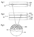
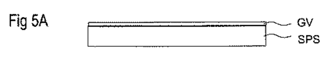
図1には本発明による支持プレートの単純な一実施形態が示されており、この実施形態においては、第1の機能層FS上にテンション層SPSが結合層VSを用いて取り付けられている。機能層FSは、例えば機能セラミックを内部に形成されたバリスタを有するバリスタセラミックの基礎上に含んでいる。 FIG. 1 shows a simple embodiment of a support plate according to the invention, in which a tension layer SPS is mounted on a first functional layer FS using a bonding layer VS. The functional layer FS includes, for example, a varistor ceramic base having a varistor formed therein.
結合層VSのために、ガラス組成物が78質量%で準備される。SiO2、19質量%酸化ホウ素、3質量%酸化カリウム。このような組成は、膨張係数に関してバリスタセラミックの材料に適合されている。ガラスの軟化点は約775°である。 For the bonding layer VS, a glass composition is prepared at 78% by weight. SiO2, 19 mass% boron oxide, 3 mass% potassium oxide. Such a composition is adapted to the material of the varistor ceramic with respect to the coefficient of expansion. The softening point of glass is about 775 °.
結合層VSは、例えば、精確に分配された形態の上述のガラス成分を含むペーストの形態で例えば印刷によって機能層FS上へ設けられる。ペースト状の結合層VSの層厚は、約2〜10μmである。 The bonding layer VS is provided on the functional layer FS by, for example, printing in the form of a paste containing the above-described glass component in a precisely distributed form. The layer thickness of the paste-like bonding layer VS is about 2 to 10 μm.
テンション層SPSのために、例えば酸化ジルコニウムを基礎とするグリーンシートが作製される。グリーンシートは、機能層FS上で結合層VS上へ積層される。 For the tension layer SPS, for example, a green sheet based on zirconium oxide is produced. The green sheet is laminated on the bonding layer VS on the functional layer FS.
つづいて、構造全体が約920℃で焼結される。この温度においては、結合層VSにおけるガラス成分が溶融し、流動化する。このとき、テンション層SPSのためのグリーンシートから結合剤のみが焼き尽くされる一方、テンション層SPSの粒子構造は、体積収縮を伴うことなく引き続き保持される。それにもかかわらず、粒子は、支持プレートあるいは構造の焼結中のテンション作用の達成に十分な高い強度が互いの間で保持される。室温へのコントロールされた冷却後に、図1に図示された構造が得られる。 Subsequently, the entire structure is sintered at about 920 ° C. At this temperature, the glass component in the bonding layer VS melts and fluidizes. At this time, only the binder is burned out from the green sheet for the tension layer SPS, while the particle structure of the tension layer SPS is continuously maintained without volume shrinkage. Nevertheless, the particles are held high enough between each other to achieve a tensioning action during sintering of the support plate or structure. After controlled cooling to room temperature, the structure illustrated in FIG. 1 is obtained.
図1に図示された構造は、電気部品のための基板として機能することが可能である。しかし、粒子状の構造を備えたテンション層SPSを基板に対する更なる処理の前に再び除去することも可能である。加えて、例えば酸化ジルコニウム粒子である、例えば適当な粒子状の媒体によるサンドブラスト、研磨粒子による湿式の研磨又はブラッシングである機械的な除去方法が考慮に値する。除去ブラッシングを多段式に行うことができ、一連の部分工程では、最後の方法工程において最も柔らかいブラシで除去ブラッシングが行われるように、異なる硬さのブラシが用いられる。 The structure illustrated in FIG. 1 can function as a substrate for electrical components. However, it is also possible to remove the tension layer SPS with a particulate structure again before further processing on the substrate. In addition, mechanical removal methods such as, for example, zirconium oxide particles, eg sand blasting with suitable particulate media, wet polishing or brushing with abrasive particles, are worth considering. The removal brushing can be performed in a multi-stage manner, and in a series of partial steps, brushes of different hardness are used so that the removal brushing is performed with the softest brush in the last method step.
焼結の前後には、機能層の寸法が決定され、したがって側方の収縮が算出される。本発明による支持プレートはx、y軸に沿って測定して1.0%よりわずかな側方の収縮を備えることが分かった。これを超える収縮は、テンション層によって阻止される。 Before and after sintering, the dimensions of the functional layer are determined and therefore the lateral shrinkage is calculated. The support plate according to the invention has been found to have a lateral shrinkage of less than 1.0% as measured along the x, y axis. Shrinkage beyond this is prevented by the tension layer.
図2には、本発明による支持プレートTPの別の一実施形態が示されており、この支持プレートにおいては、第1のテンション層SPS1に対向して第2のテンション層SPS2が第2の結合層VS2を用いて設けられている。したがって、この配置は、鏡面としての機能層FSを有する対称な構造を備えている。第2のテンション層の設置は、第1のテンション層の設置と同様になされる。両テンション層SPS1,SPS2は、互いに同期して、又は互いに連続して設けられる。焼結工程は、両テンション層に対して共通に行われる。 FIG. 2 shows another embodiment of the support plate TP according to the present invention, in which the second tension layer SPS2 is opposed to the first tension layer SPS1 and the second coupling is performed. It is provided using the layer VS2. This arrangement therefore has a symmetrical structure with the functional layer FS as a mirror surface. The second tension layer is installed in the same manner as the first tension layer. Both tension layers SPS1 and SPS2 are provided in synchronization with each other or continuously with each other. The sintering process is performed in common for both tension layers.
図3には、テンション層SPSと結合層VSと機能層FSの間の境界面における本発明による支持プレートTPの構造の一部が示されている。機能層FSは、焼結によって濃密にされているとともに、孔を有さない。表面はある程度の残留粗さを有しており、この残留粗さは、テンション層SPSの粒子構造に基づくべきである。これに対して、テンション層SPSはまだ粒子構造を有しており、この粒子構造に基づき、中間空間に元来存在する結合剤が焼結過程中に焼き尽くされている。粒子は、テンション層SPSにおいて互いに良好な付着性を備えているとともに、テンション層を機械的に安定化させ、したがってテンション作用を可能とするものである。 FIG. 3 shows part of the structure of the support plate TP according to the invention at the interface between the tension layer SPS, the coupling layer VS and the functional layer FS. The functional layer FS is made dense by sintering and has no holes. The surface has a certain degree of residual roughness, which should be based on the grain structure of the tension layer SPS. In contrast, the tension layer SPS still has a particle structure, and based on this particle structure, the binder originally present in the intermediate space is burned out during the sintering process. The particles have good adhesion to each other in the tension layer SPS and mechanically stabilize the tension layer, thus enabling a tensioning action.
結合層VSは、機能層FS及びテンション層SPSの両表面に密着するとともに、平面的に拡大された境界面によって大きな接着作用を生じさせる。それぞれ結合層VSとテンション層SPS及び機能層FSの各表面の間の境界層を境界面と呼ぶ。 The bonding layer VS is in close contact with both surfaces of the functional layer FS and the tension layer SPS, and causes a large adhesive action due to a planarly enlarged boundary surface. The boundary layers between the surfaces of the bonding layer VS, the tension layer SPS, and the functional layer FS are called boundary surfaces.
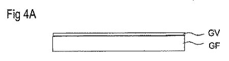
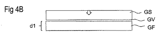
図4A〜図4Dには、第1の実施による支持プレートの製造における様々な方法段階が示されている。機能層FSのグリーン体GF上には、結合層VSの前段としてガラスペーストの層GVが最大で10μmまでの薄い層厚で設けられる。図4には配置が示されている。ガラスペーストの層GV上には、いまや、例えば、結合剤における例えば酸化ジルコニウムの基礎上の高焼結されたセラミックの粒子の密なパックを含むグリーンシートGSの積層によってテンション層SPSが設けられる。 4A to 4D show the various method steps in the production of the support plate according to the first implementation. On the green body GF of the functional layer FS, a glass paste layer GV is provided with a thin layer thickness of up to 10 μm as a preceding stage of the coupling layer VS. The arrangement is shown in FIG. On the layer GV of glass paste, a tension layer SPS is now provided, for example by lamination of a green sheet GS comprising a dense pack of highly sintered ceramic particles on the basis of eg zirconium oxide in a binder.
つづいて構造が焼結され、テンション層SPSのグリーンシートGSは、引き続きその体積を維持する。なぜなら、結合剤が燃え尽きるためである。結合層VSのガラスペースト層GVは、テンション層SPSの多孔性の表面が軟化し、流動化する。 Subsequently, the structure is sintered, and the green sheet GS of the tension layer SPS continues to maintain its volume. This is because the binder burns out. In the glass paste layer GV of the bonding layer VS, the porous surface of the tension layer SPS is softened and fluidized.
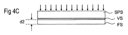
機能層FSのグリーンシート構造GFは、焼結するとともに、このとき、圧縮によって焼結収縮を生じさせる。しかし、これは、グリーンシート構造GFから機能層FSへの移行時の層厚の減少においてのみ現れる。層厚は、図4Bによる当初のd1から図4Cによるd2へ減少する。側方の収縮は、テンション層SPSによるテンションによって阻止される。焼結後の冷却時には、構造は、引き続き形状安定的及び寸法安定的なままであるとともに、熱膨張分だけ低減する。 The green sheet structure GF of the functional layer FS is sintered, and at this time, sintering shrinkage is caused by compression. However, this appears only in the reduction of the layer thickness during the transition from the green sheet structure GF to the functional layer FS. The layer thickness decreases from the original d1 according to FIG. 4B to d2 according to FIG. 4C. Lateral shrinkage is prevented by tension by the tension layer SPS. Upon cooling after sintering, the structure continues to be shape and dimensionally stable and is reduced by thermal expansion.
テンション層SPSが犠牲層として用いられれば、図4Cにおいて矢印で示唆されているようにこの犠牲層はつづいて機械的に除去される必要がある。 If the tension layer SPS is used as a sacrificial layer, this sacrificial layer must then be mechanically removed as suggested by the arrows in FIG. 4C.
図4Dには、テンション層の除去後の配置が示されている。機能層FSは、いまや、当初の結合層VSに対応するガラス層によってのみ覆われている。ガラス層あるいは結合層のより大きな硬さにより、これらガラス層あるいは結合層は、選択された除去方法に対して安定している。 FIG. 4D shows the arrangement after removal of the tension layer. The functional layer FS is now covered only by the glass layer corresponding to the original bonding layer VS. Due to the greater hardness of the glass layer or tie layer, these glass layers or tie layers are stable to the chosen removal method.
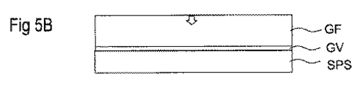
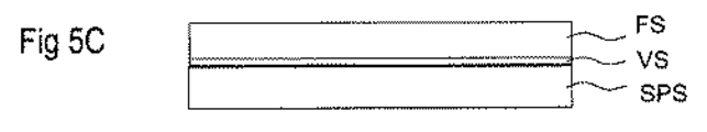
図5A〜図5Cには、第2の方法態様による本発明による支持プレートの製造における様々な方法段階が示されている。ここで、固体のプレートとして存在するテンション層SPSが起点となり、このテンション層上に、最大で10μmまでの薄い層厚の、結合層VSのためのガラスペーストGVが設けられる。図5Aには、この方法段階における配置が示されている。 5A to 5C show various method steps in the production of a support plate according to the invention according to a second method aspect. Here, the tension layer SPS present as a solid plate is a starting point, and a glass paste GV for the bonding layer VS having a thin layer thickness of up to 10 μm is provided on the tension layer. FIG. 5A shows the arrangement in this method step.
ガラス粒子の層GV上には、いまや、機能層FSのためのグリーンシートGFあるいはグリーンシートスタックが例えば積層することによって設けられている。しかし、機能層のためのグリーンシートを個別に積層することも可能である。図5Bには、機能層FSのための積層されたグリーンシートによるこの方法段階における配置が示されている。 On the glass particle layer GV, a green sheet GF or a green sheet stack for the functional layer FS is now provided, for example, by laminating. However, the green sheets for the functional layer can be individually laminated. FIG. 5B shows the arrangement in this method step with stacked green sheets for the functional layer FS.
次の工程では、図4A〜図4Dに基づき説明したものと類似のように焼結が行われる。ここでも、焼結時及び冷却時には、機能層FSのテンションが、テンション層SPSによって側方の焼結収縮を阻止し、その結果、寸法においてのみ層平面に対して垂直に焼結収縮が生じる。これに対して、図5B及び図5Cから見られるように、機能層FSのためのシートスタックの層厚又は個々の機能層FSの層厚が減少する。 In the next step, sintering is performed in a manner similar to that described with reference to FIGS. 4A to 4D. Again, during sintering and cooling, the tension of the functional layer FS prevents lateral sintering shrinkage by the tension layer SPS, resulting in sintering shrinkage perpendicular to the layer plane only in dimensions. In contrast, as can be seen from FIGS. 5B and 5C, the layer thickness of the sheet stack for the functional layer FS or the layer thickness of the individual functional layer FS decreases.
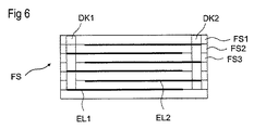
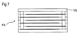
図6には、当該受動素子が後の機能層FSのためのグリーンシートGFのスタックへ組み込まれることができるように例示的な受動素子が示されている。機能セラミックのそれぞれ2つの部分層FS1,FS2,...の間には、受動素子のために、1つずつ構造化された電極層ELが配置されている。電極層ELは、少なくとも2つの貫通接続部DK1,DK2によって1つずつ交互に接続されているため、第1の電極層EL1が第1の貫通接続部DK1に接続され、その一方、第2の電極層EL2は第2の貫通接続部DK2に接続されている。このような部品構造は、例えばバリスタセラミックによって実現されることができるとともに、このときバリスタを形成する。このバリスタは、最初に調整可能な閾値電圧から、第1の電極から第2の電極へ電流を導くか、あるいは誘導する保護部品である。この閾値電圧が過電圧よりも小さければ、電圧を、閾値の到達時にこのようにして確実に誘導することが可能である。 FIG. 6 shows an exemplary passive element so that the passive element can be incorporated into a stack of green sheets GF for a later functional layer FS. Two partial layers FS1, FS2,. . . Between them, electrode layers EL structured one by one are arranged for passive elements. Since the electrode layers EL are alternately connected one by one by at least two through-connection portions DK1 and DK2, the first electrode layer EL1 is connected to the first through-connection portion DK1, while the second The electrode layer EL2 is connected to the second through connection DK2. Such a component structure can be realized, for example, by a varistor ceramic and at this time forms a varistor. The varistor is a protective component that conducts or induces current from the first electrode to the second electrode from the first adjustable threshold voltage. If this threshold voltage is smaller than the overvoltage, the voltage can be reliably induced in this way when the threshold is reached.
しかし、図6に図示された構造は、セラミックの機能層FSの部分層が誘電体で構成されている、セラミックの積層コンデンサであり得る。第1の電極層EL1と第2の電極層EL2の間に電圧を印加することで、これら両電極の間にキャパシタンスが生成される。 However, the structure shown in FIG. 6 may be a ceramic multilayer capacitor in which a partial layer of the ceramic functional layer FS is made of a dielectric. By applying a voltage between the first electrode layer EL1 and the second electrode layer EL2, a capacitance is generated between these two electrodes.
図7には、図6に図示された受動構成要素が、テンション層の焼結後及び除去後の方法生成物として示されている。機能層FS上には、いまや、元来のテンション層VSのガラス層のみがまだ存在している。 In FIG. 7, the passive component illustrated in FIG. 6 is shown as a process product after sintering and removal of the tension layer. Only the original glass layer of the tension layer VS is still present on the functional layer FS.
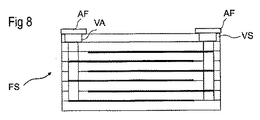
そして、単段又は多段のプロセスにおいては、貫通接続部DKの露出した上端上、及び元来の結合層VSのガラス層の表面上の隣接する縁部範囲には、接続面AFを生じさせることが可能である。第1の部分工程では、更に、例えば無電解の金属析出によって、ビアVAが元来の結合層VSのガラス層を通って延びることが可能である。つづいて、充填されたビアVA上には金属電気的な接続面AFが、例えば接触部の印刷及び焼き付けによって生じる。しかし、接触部を電気メッキ的に設けることも可能である。図8には、この方法段階における配置が示されている。 In the single-stage or multi-stage process, the connection surface AF is generated in the adjacent edge portion on the exposed upper end of the through-connection portion DK and on the surface of the glass layer of the original coupling layer VS. Is possible. In the first partial step, the via VA can further extend through the glass layer of the original bonding layer VS, for example by electroless metal deposition. Subsequently, a metal electrical connection surface AF is formed on the filled via VA by, for example, printing and baking of the contact portion. However, the contact portion can be provided by electroplating. FIG. 8 shows the arrangement in this method step.
いまや、電気部品を、接続面AF上へ電気的及び機械的に取り付けることができ、支持プレートは、部品のための支持部としての役割を担う。組み込まれた受動素子によって、支持プレートにおける保護機能を実現することができ、この支持プレートは、部品を例えば過電圧に対して保護するものである。しかし、支持プレートでは、他の受動部品機能も対応する受動構成要素の形態で実現され、部品に接続されることが可能である。 Now, the electrical component can be mounted electrically and mechanically on the connection surface AF, and the support plate serves as a support for the component. An integrated passive element can provide a protective function in the support plate, which protects the component against overvoltages, for example. However, in the support plate, other passive component functions can also be realized in the form of corresponding passive components and connected to the component.
本発明は、わずかな選択された実施例に基づいて説明され、したがって、図示の実施例及び/又は各図に限定されていない。本発明は、各請求項によってのみ定義されているとともに、その範囲において別のバリエーションを含んでいる。各請求項の特徴の下位の組合せも本発明によるものとみなされる。 The invention has been described on the basis of a few selected embodiments and is therefore not limited to the illustrated embodiments and / or figures. The present invention is defined only by the claims, and includes other variations in its scope. Subordinate combinations of the features of each claim are also considered to be according to the invention.
TP 支持プレート
FS セラミックの機能層
SPS セラミックのテンション層
VS 結合層
GV 結合層のためのガラスペースト層
CTE 熱膨張係数
GF セラミックの機能層のためのグリーン体
GS セラミックのテンション層のためのグリーン体
FS1,FS2 機能層の部分層
GS テンション層のためのグリーンシート
AF 電気的な接続面
VA 結合層を通るビア
TP support plate FS ceramic functional layer SPS ceramic tension layer VS bonding layer GV bonding layer glass paste layer CTE coefficient of thermal expansion GF green body for ceramic functional layer GS green body for ceramic tension layer FS1 , FS2 Partial layer of functional layer GS Green sheet for tension layer AF Electrical connection surface VA Via through the coupling layer
Claims (17)
−結合層(VS)と、
−セラミックのテンション層(SPS)と、
を含み、
−前記セラミックの機能層(FS)が、支持プレート(TP)のために、前記結合層(VS)を介して前記セラミックのテンション層(SPS)に結合されており、
−前記セラミックの機能層(FS)には、電気部品と接続可能な受動電気構成要素が組み込まれており、
−前記機能層(FS)及び前記テンション層(SPS)はガラスを含んでいないか、又は5質量(%)より小さなわずかなガラス割合のみを有し、
−前記結合層(VS)が、ガラス成分を含むか、又はガラス層である、
電気部品のための支持プレート。 A first ceramic functional layer;
A bonding layer (VS);
A ceramic tension layer (SPS);
Including
The ceramic functional layer (FS) is bonded to the ceramic tension layer (SPS) via the bonding layer (VS) for the support plate (TP);
The ceramic functional layer (FS) incorporates passive electrical components connectable to electrical components;
The functional layer (FS) and the tension layer (SPS) do not contain glass or have only a small glass proportion smaller than 5% by weight,
The bonding layer (VS) contains a glass component or is a glass layer,
Support plate for electrical components.
請求項1に記載の支持プレート。 The bonding layer (VS) has a thickness of 0.5 to 10 μm.
The support plate according to claim 1.
前記結合層(VS)が、前記ガラス成分のほかに、焼結されていないセラミックの充填材料を更に含んでいる、
請求項1又は2に記載の支持プレート。 The support plate according to claim 1 or 2, wherein the bonding layer (VS) further includes an unsintered ceramic filler material in addition to the glass component.
The support plate according to claim 1 or 2.
請求項1〜3のいずれか1項に記載の支持プレート。 The tension layer (SPS) has a sintering temperature exceeding the sintering temperature of the functional layer (FS) and the bonding layer (VS).
The support plate of any one of Claims 1-3.
請求項1〜4のいずれか1項に記載の支持プレート。 The tension layer (SPS) has a relatively low thermal expansion coefficient CTES that is lower than the thermal expansion coefficient CTEF of the functional layer (FS).
The support plate of any one of Claims 1-4.
請求項1〜5のいずれか1項に記載の支持プレート。 The first tension layer includes a second coupling layer (VS2) and a second tension layer (SPS2), and the second tension layer of the functional layer (FS) passes through the second coupling layer. Bound to its surface facing away from the layers, so that the support plate has a symmetrical structure with respect to layer order, material and layer thickness,
The support plate of any one of Claims 1-5.
請求項1〜6のいずれか1項に記載の支持プレート。 The at least one bonding layer (VS) includes, as a major component, oxides of Si and / or Ge, B and K, which together comprise a total of at least 70% by weight of the bonding layer. The proportion lacking up to mass% is formed of highly sintered filler material,
The support plate of any one of Claims 1-6.
請求項1〜7のいずれか1項に記載の支持プレート。 The functional layer (FS) includes a layer made of a varistor material and includes at least two electrode layers (EL1, EL2).
The support plate of any one of Claims 1-7.
請求項1〜7のいずれか1項に記載の支持プレート。 The functional layer (FS) is selected from NTC ceramic or PTC ceramic layers, ceramic multilayer capacitors, ferrite layers, piezoelectric layers and LTCC ceramics,
The support plate of any one of Claims 1-7.
請求項8又は9に記載の支持プレート。 The functional layer (FS) comprises at least two different partial layers (FS1, FS2) having at least three metallization planes structured to electrodes for different electroceramic properties and different passive electrical components; The different passive electrical components are incorporated into the functional layer;
The support plate according to claim 8 or 9.
請求項1〜10のいずれか1項に記載の支持プレート。 The tension layer (SPS) is a layer based on highly sintered oxides and compounds such as ZrO 2 , MgO, SrCO 3 , BaCO 3 or MgSiO 4 ,
The support plate according to claim 1.
b)前記グリーン体上へガラス粒子の比較的薄い層を設ける工程と、
c)セラミックのテンション層のためのグリーン体をガラス粒子上へ設ける工程と、
d)ガラス粒子及びセラミックの機能層の焼結温度より高い温度で構造を焼結する工程と、
e)前記構造をコントロールしつつ冷却する工程であって、1〜10μmの厚さのガラス層を有する固体の結合部が生じ、側方の焼結収縮が軸線ごとに3%より小さい値に制限されている、工程と、
を含む、請求項1に記載の支持プレートを製造するための方法。 a) providing a green body for a ceramic functional layer in which passive electrical components are pre-formed;
b) providing a relatively thin layer of glass particles on the green body;
c) providing a green body for the ceramic tension layer on the glass particles;
d) sintering the structure at a temperature higher than the sintering temperature of the functional layer of glass particles and ceramic;
e) Cooling process while controlling the structure, resulting in a solid joint having a glass layer with a thickness of 1-10 μm, and the lateral sintering shrinkage limited to a value less than 3% per axis A process,
A method for manufacturing a support plate according to claim 1.
請求項12に記載の方法。 The green body for the ceramic functional layer comprises at least one green sheet, wherein a layer of glass particles is provided on the at least one green sheet in the form of a paste, In the sheet, a paste or green sheet is provided on the glass particle layer as a green body for the ceramic tension layer,
The method of claim 12.
B)ガラス粒子の比較的薄い層(GV)を前記テンション層上へ設ける工程と、
C)セラミックの機能層(GF)のためのグリーン体をガラス粒子の層(GV)上へ設け、その中に受動電気構成要素をあらかじめ形成する工程と、
d)ガラス粒子及びセラミックの機能層の焼結温度より高い温度で構造を焼結する工程と、
e)前記構造をコントロールしつつ冷却する工程であって、1〜10μmの厚さのガラス層VSを有する固体の結合部が生じ、側方の焼結収縮が軸線ごとに3%より小さい値に制限されている、工程と、
を代替的に含む、請求項1に記載の支持プレートを製造するための方法。 A) providing a solid ceramic plate for the tension layer (SPS);
B) providing a relatively thin layer (GV) of glass particles on the tension layer;
C) providing a green body for a ceramic functional layer (GF) on a layer of glass particles (GV) and pre-forming passive electrical components therein;
d) sintering the structure at a temperature higher than the sintering temperature of the functional layer of glass particles and ceramic;
e) Cooling process while controlling the structure, where a solid joint having a glass layer VS with a thickness of 1 to 10 μm is generated, and the lateral sintering shrinkage is less than 3% per axis. Limited process, and
A method for manufacturing a support plate according to claim 1, comprising:
を更に含む、請求項1〜14のいずれか1項に記載の方法。 f) performing a mechanical removal method after cooling, wherein the tension layer (SPS) is removed again,
The method according to claim 1, further comprising:
電気部品のための電気的な接続面が、導電的な接触部において、前記最上の接触部と共に前記結合部上へ設けられる、請求項12〜16のいずれか1項に記載の方法。 After step E) or e), in the solid joint, the top contact of the passive component is exposed below the glass layer,
17. A method according to any one of claims 12 to 16, wherein an electrical connection surface for an electrical component is provided on the coupling part with the uppermost contact part in a conductive contact part.
Applications Claiming Priority (3)
| Application Number | Priority Date | Filing Date | Title |
|---|---|---|---|
| DE102014118749.0A DE102014118749A1 (en) | 2014-12-16 | 2014-12-16 | Low distortion ceramic carrier plate and method of manufacture |
| DE102014118749.0 | 2014-12-16 | ||
| PCT/EP2015/079813 WO2016096870A1 (en) | 2014-12-16 | 2015-12-15 | Low-warpage ceramic carrier plate and method for production |
Related Child Applications (1)
| Application Number | Title | Priority Date | Filing Date |
|---|---|---|---|
| JP2020126497A Division JP2020184646A (en) | 2014-12-16 | 2020-07-27 | Low-distortion ceramic support plate and manufacturing method thereof |
Publications (2)
| Publication Number | Publication Date |
|---|---|
| JP2017538293A true JP2017538293A (en) | 2017-12-21 |
| JP2017538293A5 JP2017538293A5 (en) | 2018-12-27 |
Family
ID=55027717
Family Applications (2)
| Application Number | Title | Priority Date | Filing Date |
|---|---|---|---|
| JP2017531824A Withdrawn JP2017538293A (en) | 2014-12-16 | 2015-12-15 | Low distortion ceramic support plate and method for manufacturing |
| JP2020126497A Pending JP2020184646A (en) | 2014-12-16 | 2020-07-27 | Low-distortion ceramic support plate and manufacturing method thereof |
Family Applications After (1)
| Application Number | Title | Priority Date | Filing Date |
|---|---|---|---|
| JP2020126497A Pending JP2020184646A (en) | 2014-12-16 | 2020-07-27 | Low-distortion ceramic support plate and manufacturing method thereof |
Country Status (6)
| Country | Link |
|---|---|
| US (1) | US20170332491A1 (en) |
| EP (1) | EP3234957A1 (en) |
| JP (2) | JP2017538293A (en) |
| CN (1) | CN107004504A (en) |
| DE (1) | DE102014118749A1 (en) |
| WO (1) | WO2016096870A1 (en) |
Families Citing this family (6)
| Publication number | Priority date | Publication date | Assignee | Title |
|---|---|---|---|---|
| KR102464070B1 (en) * | 2016-09-29 | 2022-11-07 | 주식회사 아모텍 | ESD protection device and method thereof and mobile electronic device with the same |
| KR101963283B1 (en) * | 2017-02-10 | 2019-03-28 | 삼성전기주식회사 | Capacitor Component |
| KR102404320B1 (en) * | 2017-08-31 | 2022-06-07 | 삼성전기주식회사 | Multilayer ceramic capacitor and method of manufacturing the same |
| CN111302789B (en) * | 2020-03-17 | 2021-01-19 | 华南理工大学 | Pulse energy storage dielectric material with sandwich structure and preparation method and application thereof |
| DE102020205305B4 (en) * | 2020-04-27 | 2022-06-30 | Eberspächer Catem Gmbh & Co. Kg | PTC heater and method of making same |
| CN114373632B (en) * | 2022-01-22 | 2022-09-02 | 池州昀冢电子科技有限公司 | Multilayer ceramic capacitor and method for manufacturing the same |
Citations (7)
| Publication number | Priority date | Publication date | Assignee | Title |
|---|---|---|---|---|
| JPH06143239A (en) * | 1992-11-02 | 1994-05-24 | Sumitomo Metal Ind Ltd | Manufacture of ceramic board |
| JP2002050869A (en) * | 2000-07-31 | 2002-02-15 | Kyocera Corp | Method of manufacturing multilayered wiring board |
| JP2002198647A (en) * | 2000-12-26 | 2002-07-12 | Kyocera Corp | Method of manufacturing low-temperature baked ceramic wiring board |
| WO2007004415A1 (en) * | 2005-07-01 | 2007-01-11 | Murata Manufacturing Co., Ltd. | Multilayer ceramic substrate, process for producing the same and composite green sheet for production of multilayer ceramic substrate |
| JP2008060332A (en) * | 2006-08-31 | 2008-03-13 | Sanyo Electric Co Ltd | Laminated-ceramic-substrate manufacturing method, and laminated ceramic substrate |
| JP2009522792A (en) * | 2006-01-05 | 2009-06-11 | エプコス アクチエンゲゼルシャフト | Monolithic ceramic element and fabrication method |
| JP2014160694A (en) * | 2013-02-19 | 2014-09-04 | Panasonic Corp | Ceramic wiring board and varistor built-in ceramic wiring board |
Family Cites Families (5)
| Publication number | Priority date | Publication date | Assignee | Title |
|---|---|---|---|---|
| JP3692623B2 (en) * | 1996-05-20 | 2005-09-07 | 株式会社デンソー | Ceramic laminate and manufacturing method thereof |
| JP2000208074A (en) * | 1999-01-19 | 2000-07-28 | Canon Inc | Image display device and cathode-ray tube |
| DE10145364A1 (en) * | 2001-09-14 | 2003-04-10 | Epcos Ag | Production of a ceramic substrate comprises preparing a base body having a stack of layers containing non-sintered ceramic material, arranging and fixing a rigid constrained layer to the uppermost layer of the stack, and removing |
| KR101108958B1 (en) * | 2003-02-25 | 2012-01-31 | 쿄세라 코포레이션 | Laminated ceramic capacitor and method of manufacturing the same |
| US20100103634A1 (en) * | 2007-03-30 | 2010-04-29 | Takuo Funaya | Functional-device-embedded circuit board, method for manufacturing the same, and electronic equipment |
-
2014
- 2014-12-16 DE DE102014118749.0A patent/DE102014118749A1/en not_active Withdrawn
-
2015
- 2015-12-15 JP JP2017531824A patent/JP2017538293A/en not_active Withdrawn
- 2015-12-15 WO PCT/EP2015/079813 patent/WO2016096870A1/en active Application Filing
- 2015-12-15 CN CN201580065212.0A patent/CN107004504A/en active Pending
- 2015-12-15 EP EP15817170.2A patent/EP3234957A1/en not_active Withdrawn
- 2015-12-15 US US15/531,361 patent/US20170332491A1/en not_active Abandoned
-
2020
- 2020-07-27 JP JP2020126497A patent/JP2020184646A/en active Pending
Patent Citations (7)
| Publication number | Priority date | Publication date | Assignee | Title |
|---|---|---|---|---|
| JPH06143239A (en) * | 1992-11-02 | 1994-05-24 | Sumitomo Metal Ind Ltd | Manufacture of ceramic board |
| JP2002050869A (en) * | 2000-07-31 | 2002-02-15 | Kyocera Corp | Method of manufacturing multilayered wiring board |
| JP2002198647A (en) * | 2000-12-26 | 2002-07-12 | Kyocera Corp | Method of manufacturing low-temperature baked ceramic wiring board |
| WO2007004415A1 (en) * | 2005-07-01 | 2007-01-11 | Murata Manufacturing Co., Ltd. | Multilayer ceramic substrate, process for producing the same and composite green sheet for production of multilayer ceramic substrate |
| JP2009522792A (en) * | 2006-01-05 | 2009-06-11 | エプコス アクチエンゲゼルシャフト | Monolithic ceramic element and fabrication method |
| JP2008060332A (en) * | 2006-08-31 | 2008-03-13 | Sanyo Electric Co Ltd | Laminated-ceramic-substrate manufacturing method, and laminated ceramic substrate |
| JP2014160694A (en) * | 2013-02-19 | 2014-09-04 | Panasonic Corp | Ceramic wiring board and varistor built-in ceramic wiring board |
Also Published As
| Publication number | Publication date |
|---|---|
| US20170332491A1 (en) | 2017-11-16 |
| EP3234957A1 (en) | 2017-10-25 |
| DE102014118749A1 (en) | 2016-06-16 |
| WO2016096870A1 (en) | 2016-06-23 |
| CN107004504A (en) | 2017-08-01 |
| JP2020184646A (en) | 2020-11-12 |
Similar Documents
| Publication | Publication Date | Title |
|---|---|---|
| JP2017538293A (en) | Low distortion ceramic support plate and method for manufacturing | |
| KR100821274B1 (en) | Chip Ceramic Electronic component | |
| KR101141372B1 (en) | Laminated ceramic electronic component and method for producing laminated ceramic electronic component | |
| KR101452068B1 (en) | Multi-layered ceramic capacitor and circuit board for mounting the same | |
| JP2017538293A5 (en) | ||
| JP5313289B2 (en) | Multilayer ceramic capacitor | |
| TW505932B (en) | Chip-type electronic component and manufacturing method therefor | |
| US20130222973A1 (en) | Laminated Ceramic Electronic Component and Manufacturing Method Therefor | |
| JP2008254988A (en) | Dielectric ceramics and method for producing the same, and monolithic ceramic capacitor | |
| JP2018098327A5 (en) | ||
| JP2010103987A (en) | Vibrator | |
| KR101452065B1 (en) | Multi-layered ceramic capacitor and mounting structure of circuit having thereon multi-layered ceramic capacitor | |
| WO2011122416A1 (en) | Piezoelectric-element-using device | |
| JP5960816B2 (en) | Multilayer ceramic capacitor | |
| JPWO2005104639A1 (en) | MULTILAYER CERAMIC SUBSTRATE, ITS MANUFACTURING METHOD, AND PIEZOELECTRIC RESONANT COMPONENT | |
| JP6496604B2 (en) | Electrostatic chuck and manufacturing method thereof | |
| JP2022530320A (en) | High-density corrosion-resistant layer arrangement for electrostatic chuck | |
| JP2006295418A (en) | Resonator | |
| JP5527404B2 (en) | Multilayer ceramic electronic components | |
| JP2014232850A (en) | Lamination type electronic part | |
| WO2014027553A1 (en) | Esd protection device | |
| JP2010199271A (en) | Multilayer piezoelectric element, manufacturing method thereof, and vibrator | |
| JP4144274B2 (en) | Manufacturing method of multilayer ceramic electronic component | |
| JP6306316B2 (en) | Capacitor | |
| KR102039802B1 (en) | Ceramic body for electrostatic chuck |
Legal Events
| Date | Code | Title | Description |
|---|---|---|---|
| A521 | Request for written amendment filed |
Free format text: JAPANESE INTERMEDIATE CODE: A523 Effective date: 20181119 |
|
| A621 | Written request for application examination |
Free format text: JAPANESE INTERMEDIATE CODE: A621 Effective date: 20181119 |
|
| A131 | Notification of reasons for refusal |
Free format text: JAPANESE INTERMEDIATE CODE: A131 Effective date: 20190820 |
|
| A977 | Report on retrieval |
Free format text: JAPANESE INTERMEDIATE CODE: A971007 Effective date: 20190821 |
|
| A521 | Request for written amendment filed |
Free format text: JAPANESE INTERMEDIATE CODE: A523 Effective date: 20191021 |
|
| A02 | Decision of refusal |
Free format text: JAPANESE INTERMEDIATE CODE: A02 Effective date: 20200324 |
|
| C60 | Trial request (containing other claim documents, opposition documents) |
Free format text: JAPANESE INTERMEDIATE CODE: C60 Effective date: 20200727 |
|
| C22 | Notice of designation (change) of administrative judge |
Free format text: JAPANESE INTERMEDIATE CODE: C22 Effective date: 20201222 |
|
| C13 | Notice of reasons for refusal |
Free format text: JAPANESE INTERMEDIATE CODE: C13 Effective date: 20210216 |
|
| C23 | Notice of termination of proceedings |
Free format text: JAPANESE INTERMEDIATE CODE: C23 Effective date: 20210615 |
|
| C03 | Trial/appeal decision taken |
Free format text: JAPANESE INTERMEDIATE CODE: C03 Effective date: 20210720 |
|
| C30A | Notification sent |
Free format text: JAPANESE INTERMEDIATE CODE: C3012 Effective date: 20210720 |
|
| A761 | Written withdrawal of application |
Free format text: JAPANESE INTERMEDIATE CODE: A761 Effective date: 20211115 |