JP2017532943A - Intrinsic power factor correction method and apparatus - Google Patents
Intrinsic power factor correction method and apparatus Download PDFInfo
- Publication number
- JP2017532943A JP2017532943A JP2017521091A JP2017521091A JP2017532943A JP 2017532943 A JP2017532943 A JP 2017532943A JP 2017521091 A JP2017521091 A JP 2017521091A JP 2017521091 A JP2017521091 A JP 2017521091A JP 2017532943 A JP2017532943 A JP 2017532943A
- Authority
- JP
- Japan
- Prior art keywords
- load
- voltage
- power supply
- wave
- supply voltage
- Prior art date
- Legal status (The legal status is an assumption and is not a legal conclusion. Google has not performed a legal analysis and makes no representation as to the accuracy of the status listed.)
- Pending
Links
- 238000012937 correction Methods 0.000 title claims abstract description 19
- 238000000034 method Methods 0.000 title abstract description 8
- 230000006698 induction Effects 0.000 claims abstract description 34
- 230000005540 biological transmission Effects 0.000 claims abstract description 25
- 239000003990 capacitor Substances 0.000 claims abstract description 19
- 238000002955 isolation Methods 0.000 claims description 9
- 230000010363 phase shift Effects 0.000 claims description 5
- 238000004804 winding Methods 0.000 claims description 4
- 238000001914 filtration Methods 0.000 claims description 3
- 239000004065 semiconductor Substances 0.000 claims description 3
- 230000004907 flux Effects 0.000 claims description 2
- 238000012546 transfer Methods 0.000 abstract description 13
- 238000010586 diagram Methods 0.000 description 10
- 238000006243 chemical reaction Methods 0.000 description 6
- 230000001939 inductive effect Effects 0.000 description 6
- 239000011162 core material Substances 0.000 description 5
- 230000008878 coupling Effects 0.000 description 5
- 238000010168 coupling process Methods 0.000 description 5
- 238000005859 coupling reaction Methods 0.000 description 5
- 238000013461 design Methods 0.000 description 5
- 230000009471 action Effects 0.000 description 4
- 238000005094 computer simulation Methods 0.000 description 2
- 238000010438 heat treatment Methods 0.000 description 2
- 230000006872 improvement Effects 0.000 description 2
- 230000007246 mechanism Effects 0.000 description 2
- 230000001105 regulatory effect Effects 0.000 description 2
- 238000004088 simulation Methods 0.000 description 2
- 235000013599 spices Nutrition 0.000 description 2
- 238000011282 treatment Methods 0.000 description 2
- 238000003466 welding Methods 0.000 description 2
- 230000009286 beneficial effect Effects 0.000 description 1
- 230000033228 biological regulation Effects 0.000 description 1
- 238000010411 cooking Methods 0.000 description 1
- 230000001627 detrimental effect Effects 0.000 description 1
- 238000005868 electrolysis reaction Methods 0.000 description 1
- 238000009713 electroplating Methods 0.000 description 1
- 230000008030 elimination Effects 0.000 description 1
- 238000003379 elimination reaction Methods 0.000 description 1
- 230000005669 field effect Effects 0.000 description 1
- 230000007257 malfunction Effects 0.000 description 1
- 238000000691 measurement method Methods 0.000 description 1
- 238000002844 melting Methods 0.000 description 1
- 230000008018 melting Effects 0.000 description 1
- 238000012806 monitoring device Methods 0.000 description 1
- 238000012544 monitoring process Methods 0.000 description 1
- 238000007747 plating Methods 0.000 description 1
- 230000009467 reduction Effects 0.000 description 1
- 238000005476 soldering Methods 0.000 description 1
- 230000009466 transformation Effects 0.000 description 1
Images


Classifications
-
- H—ELECTRICITY
- H02—GENERATION; CONVERSION OR DISTRIBUTION OF ELECTRIC POWER
- H02M—APPARATUS FOR CONVERSION BETWEEN AC AND AC, BETWEEN AC AND DC, OR BETWEEN DC AND DC, AND FOR USE WITH MAINS OR SIMILAR POWER SUPPLY SYSTEMS; CONVERSION OF DC OR AC INPUT POWER INTO SURGE OUTPUT POWER; CONTROL OR REGULATION THEREOF
- H02M1/00—Details of apparatus for conversion
- H02M1/42—Circuits or arrangements for compensating for or adjusting power factor in converters or inverters
- H02M1/4208—Arrangements for improving power factor of AC input
- H02M1/4258—Arrangements for improving power factor of AC input using a single converter stage both for correction of AC input power factor and generation of a regulated and galvanically isolated DC output voltage
-
- H—ELECTRICITY
- H02—GENERATION; CONVERSION OR DISTRIBUTION OF ELECTRIC POWER
- H02J—CIRCUIT ARRANGEMENTS OR SYSTEMS FOR SUPPLYING OR DISTRIBUTING ELECTRIC POWER; SYSTEMS FOR STORING ELECTRIC ENERGY
- H02J50/00—Circuit arrangements or systems for wireless supply or distribution of electric power
- H02J50/10—Circuit arrangements or systems for wireless supply or distribution of electric power using inductive coupling
- H02J50/12—Circuit arrangements or systems for wireless supply or distribution of electric power using inductive coupling of the resonant type
-
- H—ELECTRICITY
- H02—GENERATION; CONVERSION OR DISTRIBUTION OF ELECTRIC POWER
- H02J—CIRCUIT ARRANGEMENTS OR SYSTEMS FOR SUPPLYING OR DISTRIBUTING ELECTRIC POWER; SYSTEMS FOR STORING ELECTRIC ENERGY
- H02J7/00—Circuit arrangements for charging or depolarising batteries or for supplying loads from batteries
- H02J7/02—Circuit arrangements for charging or depolarising batteries or for supplying loads from batteries for charging batteries from ac mains by converters
- H02J7/04—Regulation of charging current or voltage
-
- H—ELECTRICITY
- H02—GENERATION; CONVERSION OR DISTRIBUTION OF ELECTRIC POWER
- H02M—APPARATUS FOR CONVERSION BETWEEN AC AND AC, BETWEEN AC AND DC, OR BETWEEN DC AND DC, AND FOR USE WITH MAINS OR SIMILAR POWER SUPPLY SYSTEMS; CONVERSION OF DC OR AC INPUT POWER INTO SURGE OUTPUT POWER; CONTROL OR REGULATION THEREOF
- H02M1/00—Details of apparatus for conversion
- H02M1/0048—Circuits or arrangements for reducing losses
- H02M1/0054—Transistor switching losses
- H02M1/0058—Transistor switching losses by employing soft switching techniques, i.e. commutation of transistors when applied voltage is zero or when current flow is zero
-
- H—ELECTRICITY
- H02—GENERATION; CONVERSION OR DISTRIBUTION OF ELECTRIC POWER
- H02M—APPARATUS FOR CONVERSION BETWEEN AC AND AC, BETWEEN AC AND DC, OR BETWEEN DC AND DC, AND FOR USE WITH MAINS OR SIMILAR POWER SUPPLY SYSTEMS; CONVERSION OF DC OR AC INPUT POWER INTO SURGE OUTPUT POWER; CONTROL OR REGULATION THEREOF
- H02M1/00—Details of apparatus for conversion
- H02M1/14—Arrangements for reducing ripples from dc input or output
-
- H—ELECTRICITY
- H02—GENERATION; CONVERSION OR DISTRIBUTION OF ELECTRIC POWER
- H02M—APPARATUS FOR CONVERSION BETWEEN AC AND AC, BETWEEN AC AND DC, OR BETWEEN DC AND DC, AND FOR USE WITH MAINS OR SIMILAR POWER SUPPLY SYSTEMS; CONVERSION OF DC OR AC INPUT POWER INTO SURGE OUTPUT POWER; CONTROL OR REGULATION THEREOF
- H02M1/00—Details of apparatus for conversion
- H02M1/42—Circuits or arrangements for compensating for or adjusting power factor in converters or inverters
- H02M1/4208—Arrangements for improving power factor of AC input
- H02M1/4241—Arrangements for improving power factor of AC input using a resonant converter
-
- Y—GENERAL TAGGING OF NEW TECHNOLOGICAL DEVELOPMENTS; GENERAL TAGGING OF CROSS-SECTIONAL TECHNOLOGIES SPANNING OVER SEVERAL SECTIONS OF THE IPC; TECHNICAL SUBJECTS COVERED BY FORMER USPC CROSS-REFERENCE ART COLLECTIONS [XRACs] AND DIGESTS
- Y02—TECHNOLOGIES OR APPLICATIONS FOR MITIGATION OR ADAPTATION AGAINST CLIMATE CHANGE
- Y02B—CLIMATE CHANGE MITIGATION TECHNOLOGIES RELATED TO BUILDINGS, e.g. HOUSING, HOUSE APPLIANCES OR RELATED END-USER APPLICATIONS
- Y02B70/00—Technologies for an efficient end-user side electric power management and consumption
- Y02B70/10—Technologies improving the efficiency by using switched-mode power supplies [SMPS], i.e. efficient power electronics conversion e.g. power factor correction or reduction of losses in power supplies or efficient standby modes
Abstract
【解決手段】 内在的なライン力率補正を有する共振誘導無線電力伝送装置は、特定の力率補正回路を用いずに、ライン接続点にほぼ力率1の高調波歪みの小さな負荷を伴う無線伝送方法を提供する。前記装置は、従来の直流電圧の代わりに整流正弦波供給電圧によって動作する伝送周波数インバータを提供する。共振誘導転送コイル対は、2つの直列接続された特定の値の共振コンデンサを追加することによりインピーダンスインバータに変換される。前記インピーダンスインバータは、軽負荷の条件下で前記2次側電圧を上昇させ、このようにすることにより、ライン周波数の電源電流と2次側負荷電流とを比例させることにより、ライン負荷の力率をほぼ1に維持し、高調波電流の歪みを小さく抑える。【選択図】 図3A resonance induction wireless power transmission device having an inherent line power factor correction is a wireless device with a load having a small harmonic distortion having a power factor of 1 at a line connection point without using a specific power factor correction circuit. A transmission method is provided. The apparatus provides a transmission frequency inverter that operates with a rectified sinusoidal supply voltage instead of a conventional DC voltage. The resonant induction transfer coil pair is converted to an impedance inverter by adding two series-connected specific value resonant capacitors. The impedance inverter raises the secondary side voltage under light load conditions, and in this way makes the power frequency of the line load proportional to the power frequency of the line frequency and the secondary side load current. Is kept at approximately 1, and distortion of the harmonic current is kept small. [Selection] Figure 3
Description
本出願は、2014年10月20日付けで出願された米国特許仮出願第62/065,889号に対して優先権を主張するものである。当該出願の内容は、この参照により本明細書に組み込まれる。 This application claims priority to US Provisional Application No. 62 / 065,889, filed October 20, 2014. The contents of that application are incorporated herein by this reference.
本発明は、共振誘導による電気エネルギーの伝送に関する。より具体的には、本発明は、特定の力率補正回路を用いずにライン接続点においてほぼ力率1の高調波歪みの小さな負荷を提供する無線伝送の方法に関する。その代わりに、本明細書内で説明する装置は、特定の力率補正段を必要とせずに高調波歪みの小さなほぼ力率1を提供することにより、構成要素のコスト、装置のサイズ、および電力変換損失を低減する。 The present invention relates to transmission of electrical energy by resonance induction. More specifically, the present invention relates to a method of wireless transmission that provides a load having a small harmonic distortion with a power factor of approximately 1 at a line connection point without using a specific power factor correction circuit. Instead, the devices described herein provide component power, device size, and device power by providing a near power factor of 1 with low harmonic distortion without the need for a specific power factor correction stage. Reduce power conversion loss.
誘導電力伝送は、多くの産業および市場にわたって多くの重要な用途を有する。本明細書内に含まれる開示は、本発明の、比較的大電力(100ワット超)を必要とする用途への使用を企図するものの、電力用途の潜在的なリストは限定されず、本発明は、広い範囲にわたる所要電力に適用することができる。 Inductive power transfer has many important applications across many industries and markets. While the disclosure contained herein contemplates the use of the present invention for applications that require relatively high power (greater than 100 watts), the potential list of power applications is not limited, and the present invention Can be applied to a wide range of power requirements.
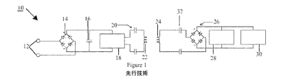
図1は、従来技術による共振誘導電力伝送システム10の概念図を示している。図示のように、ACライン12に交流ライン周波数の電気エネルギーの供給源が提供されており、ライン周波数整流器14およびシャント・コンデンサ・リップル・フィルタ16によって直流に変換される。DC/ACインバータ18が直流エネルギーを高周波交流に変換し、これが共振ネットワーク20によって1次側誘導コイル22に印加される。一般的な動作周波数は、15〜50kHzの範囲である。
FIG. 1 shows a conceptual diagram of a resonant induction
1次側誘導コイル22と2次側誘導コイル24との間の電磁結合によって1次側エネルギーが2次側に転送され、高周波整流器26によって整流され、リップルフィルタ28によってリップル濾波され、遠隔配置された電池30を充電するために使用される。共振ネットワーク32が2次側誘導コイル24を共振させることにより、最大電流の流れおよび最大エネルギーの転送を可能とする。
The primary side energy is transferred to the secondary side by electromagnetic coupling between the primary
図1の回路内のACライン接続に与えられる負荷の性質は、ライン整流器およびシャント・リップル・フィルタ・コンデンサの組み合わせによって決定される。動作時には、整流後の瞬時ライン電圧がシャントコンデンサ電圧を超えない限り、ライン整流器電流はゼロである。このことは、整流器電流が正弦波ではなく、その代わりにライン電圧正弦波が最大値に達する直前に発生する幅の狭いパルスであることを意味する。整流器電流は、正弦波の代わりに幅の狭いパルスであるので、かなりの高調波成分を含んでいる。関連付けられるライン周波数の高調波電流は、配電用の構成要素および配電システムに接続されているその他の負荷にとって有害であり、このため、電力会社または政府の規制によって低振幅に制限されている。 The nature of the load applied to the AC line connection in the circuit of FIG. 1 is determined by the combination of line rectifier and shunt ripple filter capacitor. In operation, the line rectifier current is zero unless the instantaneous rectified line voltage exceeds the shunt capacitor voltage. This means that the rectifier current is not a sine wave, but instead is a narrow pulse that occurs just before the line voltage sine wave reaches its maximum value. Since the rectifier current is a narrow pulse instead of a sine wave, it contains significant harmonic components. The associated line frequency harmonic currents are detrimental to power distribution components and other loads connected to the power distribution system and are therefore limited to low amplitudes by utility or government regulations.
別の難題として、ライン周波数整流器の電流のピークがライン周波数の最大電圧よりも前に発生するということがある。このことは、ライン周波数整流器の電流パルスの基本波成分がライン周波数の正弦波電圧に先行し、同じく規制当局による制限の対象である好ましくない進み電流の要因を生むことを意味する。ライン周波数のリップルフィルタであるシャントコンデンサ16の静電容量を増加させると、直流ライン周波数のリップルの大きさが低減されるが、しかしまた不必要に整流器電流パルスの大きさを増加させかつ幅を減少させるので、好ましくないライン周波数の高調波歪みおよび許容できないライン力率を増加させることとなる。
Another challenge is that the line frequency rectifier current peaks occur before the maximum line frequency voltage. This means that the fundamental component of the line frequency rectifier current pulse precedes the sinusoidal voltage at the line frequency and creates an undesirable lead current factor that is also subject to restrictions by the regulatory authority. Increasing the capacitance of the
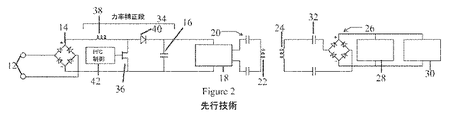
このとき問題となるのは、ライン電圧源から同相の正弦波電流を引き出しながら、如何にしてライン周波数の交流を直流に変換するかということである。図2は、この問題に対する従来の解決策、即ち、力率補正段34の追加を示している。力率補正をこのように使用することは、整流器によって生成されるライン周波数の高調波歪みの排除ならびにライン周波数の正弦波電圧および正弦波電流の位相合わせの両方を意味することに留意されたい。 The problem at this time is how to convert the alternating current of the line frequency into the direct current while extracting the in-phase sine wave current from the line voltage source. FIG. 2 shows a conventional solution to this problem, namely the addition of a power factor correction stage 34. Note that this use of power factor correction implies both elimination of line frequency harmonic distortion generated by the rectifier and phasing of sinusoidal voltage and sinusoidal current at the line frequency.
図2に示す力率補正段34は、DC/DC昇圧コンバータで構成されているものの、降圧コンバータおよび昇降圧コンバータのトポロジーを用いることもできる。シャント電界効果トランジスタ36として図2に図示されているシャント開閉器は、パルス幅によってインダクタ電流を制御し、したがって、ACライン電流を制御する。シャントトランジスタ36がオンであるとき、インダクタ電流が、整流後の瞬時ライン電圧に比例した割合で増加する。シャントトランジスタ36がオフとなると、インダクタ38に蓄積されているエネルギーが、直列ダイオード40を通ってシャント・フィルタ・コンデンサ16に投入される。制御回路42が、整流後のライン電流を監視し、整流後のライン電流がライン電圧に比例した状態が維持されるように、トランジスタの導通間隔を持続的に調節する。このようにすれば、ライン周波数整流器の電流がライン電圧振幅に比例する正弦半波となり、高調波歪みが強制的にゼロとなり、力率が強制的にほぼ1となり、DC/ACインバータの供給電圧が本質的に一定に保持される。
Although the power factor correction stage 34 shown in FIG. 2 is formed of a DC / DC boost converter, a topology of a step-down converter and a step-up / step-down converter can also be used. The shunt switch shown in FIG. 2 as shunt
しかし、図2に図示した従来の力率補正の方法には少なくとも2つの明確な不利点がある。即ち、追加の電力変換段が装置のコストおよび体積を増加させ、また不要なエネルギー変換損失をも招くことである。このような特定の力率補正回路を用いずに、共振誘導電力伝送システム内のライン接続点に、ほぼ力率1の高調波歪みの小さな負荷を提供することが望ましい。本発明は、当該技術分野におけるこの必要性に対処する。 However, the conventional power factor correction method illustrated in FIG. 2 has at least two distinct disadvantages. That is, the additional power conversion stage increases the cost and volume of the device and introduces unnecessary energy conversion losses. Instead of using such a specific power factor correction circuit, it is desirable to provide a load with a small harmonic distortion with a power factor of approximately 1 at a line connection point in the resonant induction power transmission system. The present invention addresses this need in the art.
本発明は、前記共振誘導無線電力装置の動作パラメータを変更して、追加的なエネルギー変換力率補正を必要とせずに、高調波歪みの小さなほぼ力率1のライン負荷を内在的に提供することにより、従来技術の上述の制約に対処する。従来の回路の整流器の後段のライン周波数のリップルフィルタおよびシャントコンデンサが削除され、前記DC/ACインバータは、平滑化された一定値のDC電圧によってではなく、前記ライン正弦波の全波整流に由来する正弦半波によって電力供給される。 The present invention modifies the operating parameters of the resonant inductive wireless power device to inherently provide a near power factor 1 line load with low harmonic distortion without the need for additional energy conversion power factor correction. This addresses the above-mentioned limitations of the prior art. The line frequency ripple filter and shunt capacitor after the rectifier of the conventional circuit are eliminated, and the DC / AC inverter is derived from the full wave rectification of the line sine wave, not by a smoothed constant value DC voltage. Powered by a half-sine wave.
例示的な実施形態において、前記DC/ACインバータによって生成された高周波矩形波の包絡線はもはや一定ではなく、正弦半波の形状で連続的に変化する。前記従来の伝送コイル対が、前記共振伝送コイル対が前記システム負荷電流の大きさを、したがって前記ACライン電流を、前記ACライン電圧に比例させこれと同相とする90度の伝送位相ずれを有する共振インピーダンスインバータとなるように具体的に選択された値の共振コンデンサと結合しているので、ほぼ力率1のAC負荷および小さなACライン高調波電流成分が保証される。 In an exemplary embodiment, the high frequency square wave envelope generated by the DC / AC inverter is no longer constant and varies continuously in the shape of a sine half wave. The conventional transmission coil pair has a 90 degree transmission phase shift in which the resonant transmission coil pair is proportional to the magnitude of the system load current, and thus the AC line current is proportional to and in phase with the AC line voltage. Since it is coupled with a resonant capacitor of a value specifically selected to be a resonant impedance inverter, an AC load with a power factor of approximately 1 and a small AC line harmonic current component are guaranteed.
前記無線電力伝送コイル対の2次側で、整流器が前記伝送周波数の正弦波を整流する。整流器の後段のフィルタが前記インバータ周波数のリップルを除去し、ライン周波数の正弦半波電流を前記一定DC電圧の負荷に供給する。3相AC電源電圧(three phase AC line source)の実施形態において、前記負荷に供給される電流は、相互に120度ずれた3相の整流正弦波の総和であり、したがって、低減されたライン周波数のリップルを有する。 On the secondary side of the wireless power transmission coil pair, a rectifier rectifies the sine wave of the transmission frequency. A filter after the rectifier removes the inverter frequency ripple and supplies a line frequency sine half-wave current to the constant DC voltage load. In an embodiment of a three-phase AC line source, the current supplied to the load is the sum of three-phase rectified sine waves that are offset from each other by 120 degrees, and thus a reduced line frequency. Have ripples.
前記例示的な実施形態において、本発明は、ほぼ1のACライン力率を維持し、ACライン高調波電流成分を小さく抑える装置を提供する。前記システムは、前記伝送側に、ライン周波数のリップルフィルタをその後段に有さないライン周波数整流器と、前記整流後ACライン周波数を正弦半波の形状で連続的に変化する振幅を有する包絡線変調された高周波矩形波形に変換するDC/ACインバータと、共振伝送コイル対が90度の伝送位相ずれを有する共振インピーダンスインバータとなるように具体的に選択された値を有する共振コンデンサと結合された前記伝送コイル対と、1次側誘導コイルとを含んでいる。前記受け取り側では、前記システムは、前記受け取り側の負荷に正弦半波の非交番DC電流を提供する伝送周波数整流器とこれに関連付けられる伝送周波数のリップルフィルタとを含んでいる。 In the exemplary embodiment, the present invention provides an apparatus that maintains an AC line power factor of approximately unity and keeps the AC line harmonic current component small. The system includes a line frequency rectifier that does not have a line frequency ripple filter in the transmission side on the transmission side, and an envelope modulation having an amplitude that continuously changes the AC line frequency after rectification in the form of a sine half wave. The DC / AC inverter for converting to a high frequency rectangular waveform and the resonant capacitor having a value specifically selected so that the resonant transmission coil pair is a resonant impedance inverter having a transmission phase shift of 90 degrees. A transmission coil pair and a primary induction coil are included. On the receiving side, the system includes a transmission frequency rectifier that provides a sinusoidal half-wave non-alternating DC current to the receiving load and an associated transmission frequency ripple filter.
別の実施形態において、本発明は、前記電力がDC電源からAC負荷に流れる用途に使用される。このような実施形態において、前記内在的力率補正装置は、DC電源と、前記DC電源の出力のライン周波数のリップルを濾波するシャント・リップル・フィルタ・コンデンサと、前記シャント・リップル・フィルタ・コンデンサの出力から供給されるライン周波数のリップルを濾波したDC電圧を出力方形波電圧に変換するDC/ACインバータと、前記出力方形波電圧を、ライン周波数の正弦波によって包絡線変調された前記DC/ACインバータの周波数の正弦波に変換して双極正弦波包絡線を形成するインピーダンスインバータと、前記双極正弦波包絡線を単極正弦半波包絡線に変換する2次側整流器と、前記単極正弦半波包絡線における1つおきの周期の極性を反転させて正弦波形を発生させる整流戻し(de−rectification)ネットワークと、前記正弦波形を受け取るAC負荷とを含んでいる。前記AC電源およびDC負荷の場合のように、前記インピーダンスインバータは、軽負荷条件下において2次側電圧を上昇させることにより、前記DC電源電圧から供給されるライン周波数の電源電流および前記AC負荷における電流を比例させてほぼ1力率のライン負荷力率を維持し、高調波電流の歪みを小さく抑える。例示的な実施形態において、これは、ターマンインピーダンス反転ネットワークを前記インピーダンスネットワークとして使用して前記ターマンインピーダンス反転ネットワークの2次側における瞬時負荷電圧と共に変化する変圧を提供することにより達成される。また、前記単極正弦半波包絡線が前記整流戻しネットワークに印加される前に前記単極正弦半波包絡線から高周波リップルを除去するために、リップル・フィルタ・ネットワークを提供してもよい。前記整流戻しネットワーク自体が、半波ブリッジ構成または全波ブリッジ構成の電力半導体スイッチを含むこともできる。 In another embodiment, the present invention is used in applications where the power flows from a DC power source to an AC load. In such an embodiment, the intrinsic power factor correction device includes a DC power supply, a shunt ripple filter capacitor that filters ripples of a line frequency of the output of the DC power supply, and the shunt ripple filter capacitor. A DC / AC inverter that converts a DC voltage filtered from a line frequency ripple supplied from the output to an output square wave voltage, and the output square wave voltage is envelope-modulated by a sine wave of the line frequency. An impedance inverter that converts to a sine wave of the frequency of the AC inverter to form a bipolar sine wave envelope, a secondary rectifier that converts the bipolar sine wave envelope to a single pole sine half wave envelope, and the single pole sine A rectification return that degenerates the polarity of every other period in the half-wave envelope to generate a sinusoidal waveform tion) and the network, and a AC load for receiving the sinusoidal waveform. As in the case of the AC power source and the DC load, the impedance inverter increases the secondary side voltage under light load conditions, so that the line frequency power source current supplied from the DC power source voltage and the AC load The line load power factor of approximately 1 power factor is maintained by making the current proportional, and distortion of the harmonic current is kept small. In an exemplary embodiment, this is accomplished by providing a transformer that varies with the instantaneous load voltage on the secondary side of the Turman impedance reversal network using a Turman impedance reversal network as the impedance network. A ripple filter network may also be provided to remove high frequency ripple from the unipolar sine half wave envelope before the unipolar sine half wave envelope is applied to the rectifying return network. The rectifying return network itself may also include a power semiconductor switch in a half wave bridge configuration or a full wave bridge configuration.
さらに別の実施形態において、独立した3つのDC/ACインバータストリングを使用して3相AC系統負荷が提供されており、各ストリングが、全体としてAC3相定電圧負荷を構成する前記3つのAC定電圧負荷のうちの1個を駆動する。各ストリングに絶縁変圧器を使用して前記DC電源と前記AC負荷との間にガルバニック絶縁を提供してもよい。また、前記DC電源は、3つの独立した等電圧のDC電源を含むこともでき、または3つのDC源ノードを束ねて、これに単一DC電源によって電力供給してもよい。 In yet another embodiment, a three-phase AC grid load is provided using three independent DC / AC inverter strings, and each of the three AC constants constitutes an AC three-phase constant voltage load as a whole. Drives one of the voltage loads. An isolation transformer may be used for each string to provide galvanic isolation between the DC power source and the AC load. The DC power source may include three independent equal voltage DC power sources, or three DC source nodes may be bundled and powered by a single DC power source.
添付の図に関連する以下の詳細な説明により、本発明の前述のおよびその他の有益な特徴および利点が明白となるであろう。
本発明は、本開示の一部をなす添付の図および例に関連してなされる以下の詳細な説明を参照することにより、より容易に理解することができる。本発明は本明細書内で説明されおよび/または図示される特定の製品、方法、条件またはパラメータに限定されず、かつ本明細書内で使用される専門用語は具体的な実施形態を例として説明することのみを目的とし、請求されるいずれの発明をも限定することは意図されていないことを理解すべきである。同様に、考え得る作用機序もしくは作用様式または改良の理由に関する一切の説明は例示的であることのみが意図され、本明細書内の発明は、このような提案される作用機序もしくは作用様式または改良の理由の正確さもしくは不正確さのいずれによっても制約されるものではない。 The present invention may be understood more readily by reference to the following detailed description, taken in conjunction with the accompanying drawings and examples, which form a part of this disclosure. The present invention is not limited to the particular products, methods, conditions or parameters described and / or illustrated herein, and the terminology used herein is by way of example in the specific embodiment. It should be understood that this is for illustrative purposes only and is not intended to limit any claimed invention. Similarly, any explanation as to possible mechanisms or modes of action or reasons for improvement is intended to be exemplary only, and the invention herein is intended to illustrate such proposed mechanisms or modes of action. It is not limited by the accuracy or inaccuracy of the reason for improvement.
ここで、図3〜11を参照しながら本発明の例示的な実施形態の詳細な説明を行う。この説明は本発明の考え得る実施態様の詳細な例を提供するものの、これらの詳細は例示的であることが意図されており、決して本発明の範囲を定めるものではないことに留意すべきである。 A detailed description of exemplary embodiments of the present invention will now be given with reference to FIGS. While this description provides detailed examples of possible embodiments of the invention, it should be noted that these details are intended to be exemplary and do not in any way define the scope of the invention. is there.
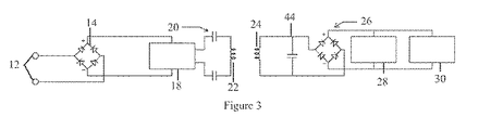
これから説明するように、本明細書内で説明し図3に示すシステムは、共振誘導による電池の無線充電器に関連して説明されるものの、当業者には、本発明はその他数多の用途を有することが明白となるであろう。当業者であれば、図3の実施形態が、共振誘導による電池の無線充電の従来の実施とは多くの点において異なることを理解するであろう。例えば、電池の充電電流は一定ではなく、正弦半波、即ち、整流正弦波の形状で変化する。このようにすれば、電池の充電電流が単相AC正弦波電源電圧と比例しかつ同相となる。前記2次側整流器の負荷インピーダンスは非線形であり、小さなテブナン抵抗を有する定電圧負荷としてふるまうと理解される。印加される前記交流電圧が前記電池の端子電圧を超えない限り、前記2次側整流器には電流は流れない。前記1次側および2次側の誘導コイル対22、24およびこれに関連付けられる共振コンデンサ20、44は、軽負荷の条件下で昇圧ネットワークとして機能するように構成することができる。このような共振LCネットワークは、軽負荷の条件下では本来的に高Q値であり、共振周波数において高い昇圧比が可能である。
As will now be described, while the system described herein and illustrated in FIG. 3 will be described in connection with a wireless charger for resonance-induced batteries, the present invention has many other uses. It will be clear to have Those skilled in the art will appreciate that the embodiment of FIG. 3 differs in many respects from the conventional implementation of wireless charging of a battery by resonance induction. For example, the charging current of the battery is not constant and changes in the shape of a sine half wave, that is, a rectified sine wave. In this way, the charging current of the battery is proportional to and in phase with the single-phase AC sine wave power supply voltage. It is understood that the load impedance of the secondary rectifier is non-linear and behaves as a constant voltage load with a small Thevenin resistance. As long as the applied AC voltage does not exceed the terminal voltage of the battery, no current flows through the secondary rectifier. The primary and secondary induction coil pairs 22 and 24 and the
整流器電流が流れていない期間、前記2次側共振回路における抵抗損失はゼロであり、瞬時負荷のかかったQ値は非常に高く、著しい変圧が発生する。このような瞬時無負荷条件下において、前記2次側整流器26に印加される共振回路出力電圧は、これが前記電池の端子電圧を超え、電池電流が流れ始めるまで増加する。設計が適切な場合、前記ライン周波数の半周期の期間を通じて前記2次側の電池充電電流を前記ACライン電圧の絶対値に比例して流すことにより、特定の力率補正段を使用せずに前記ACライン周波数電源に対して歪みの小さな力率1の負荷を与えることができる。
During the period when the rectifier current is not flowing, the resistance loss in the secondary side resonance circuit is zero, the Q value subjected to the instantaneous load is very high, and a significant transformation occurs. Under such an instantaneous no-load condition, the resonant circuit output voltage applied to the
本明細書内で説明する発明は、各ライン半周期にわたって前記ライン電流と前記ライン電圧との間の比例関係を維持するために必要な電池端子における瞬時インピーダンスの関数として連続的に変化する変圧を提供するインピーダンスインバータを使用する。当業者にとって公知であるように、インピーダンスインバータは、一方のポートに低インピーダンスを与えると他方のポートに高インピーダンスが生じる、2つのポートを有する双方向ネットワークである。 The invention described herein describes a transformer that varies continuously as a function of the instantaneous impedance at the battery terminals required to maintain a proportional relationship between the line current and the line voltage over each line half-cycle. Use the provided impedance inverter. As is known to those skilled in the art, an impedance inverter is a bi-directional network having two ports, where a low impedance at one port results in a high impedance at the other port.
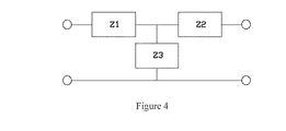
λ/4伝送線路変成器は、インピーダンスインバータの実施態様の例である。インピーダンスインバータの実現は、伝送線路による実施態様に限定されない。例えば、梯子回路網を含む複数の集中定数回路構成がある。本発明は、Terman(Radio Engineersハンドブック初版、McGraw Hill社、1943年)によって説明され、図4に示す、3素子T型インピーダンス整合ネットワークを使用する。ターマンインピーダンス整合ネットワークのリアクタンスは以下のように求められる。 A λ / 4 transmission line transformer is an example of an implementation of an impedance inverter. The realization of the impedance inverter is not limited to an embodiment with a transmission line. For example, there are a plurality of lumped constant circuit configurations including a ladder network. The present invention is described by Terman (Radio Engineers Handbook First Edition, McGraw Hill, 1943) and uses the three-element T-type impedance matching network shown in FIG. The reactance of the terman impedance matching network is obtained as follows.

但し、R1は前記2つのポートの電源インピーダンス、R2は前記2つのポートの負荷インピーダンス、およびβは前記ネットワークを通過したときに生じる位相ずれで、ラジアンで表される。前記T型インピーダンス整合ネットワークは、90度の Where R 1 is the power impedance of the two ports, R 2 is the load impedance of the two ports, and β is the phase shift that occurs when passing through the network, expressed in radians. The T-type impedance matching network is 90 degrees.
![]()
![]()
例示的な実施形態において、R1およびR2の値は一定ではなく、整流後の各半周期の期間に連続的に変化する。前記幾何学的積 In the exemplary embodiment, the values of R 1 and R 2 are not constant and vary continuously during each half-cycle period after rectification. Geometric product
図5は、共振誘導無線電力コイル対をどのようにして共振ターマン・インピーダンス・インバータに変換できるかを示している。図5Aは、19kHzで0.385の結合係数を有する無線電力伝送コイル対の無線電力コイル対等価回路を示している。前記1次側および2次側の130μHの巻線インダクタンスならびに50μHの相互インダクタンスは、19kHzでそれぞれ+j17.9および+j5.97のリアクタンスを有する。 FIG. 5 illustrates how a resonant inductive wireless power coil pair can be converted to a resonant terman impedance inverter. FIG. 5A shows a wireless power coil pair equivalent circuit of a wireless power transmission coil pair having a coupling coefficient of 0.385 at 19 kHz. The primary and secondary 130 μH winding inductance and 50 μH mutual inductance have reactances of + j17.9 and + j5.97, respectively, at 19 kHz.
図5Bにおいて、図5Aの等価回路のネットワークの直列辺に共振コンデンサ46、48が追加されている。前記リアクタンスは、19kHzにおける前記直列インダクタZ1、Z2のリアクタンスを完全に相殺し、同様に19kHzにおいてシャントの相互インダクタンス要素Z3のリアクタンスと同じ大きさの追加的な直列容量性リアクタンスを追加するように選択されている。その結果得られる図5Cのネットワークは、無線電力転送用の結合インダクタ対を組み込んだインピーダンス反転2ポート等価回路である。
In FIG. 5B,
図5Cのインピーダンス反転ネットワークは、以下のように、誘導無線電力転送ライン電流の高調波歪みを低減し、または排除する。前記ライン電圧ゼロ交差の直後には、前記整流後ライン電圧の大きさおよび前記インバータ電圧出力の大きさは小さい。前記自動車用電池30に提供される整流電流は、ゼロであるかまたは非常に小さい。前記ターマン・インピーダンス・インバータの2次側のインピーダンスは非常に高く、したがって、前記インピーダンスインバータの1次側のインピーダンスは非常に低い。前記インピーダンスインバータは低インピーダンス負荷を見て、大きな1次側電流を供給する。前記2次側電圧は、前記電池電圧を超えるまで上昇する。電池充電電流が流れ始め、前記インバータの見るインピーダンスが上昇し、前記システムが適度のライン電流、適度のインバータ電流、および適度の電池充電電流で安定する。
The impedance inversion network of FIG. 5C reduces or eliminates harmonic distortion of the inductive wireless power transfer line current as follows. Immediately after the zero crossing of the line voltage, the magnitude of the rectified line voltage and the magnitude of the inverter voltage output are small. The rectified current provided to the
前記ライン電圧周期のピーク付近では、前記整流後ライン電圧の大きさおよび前記インピーダンスインバータ電圧出力の大きさは大きい。前記自動車用電池に提供される整流電流もまた、大きい。前記ターマン・インピーダンス・インバータの2次側のインピーダンスは低く、したがって、前記インピーダンスインバータの1次側のインピーダンスは比較的高い。前記インピーダンスインバータの補償作用が、前記ライン電流および前記電池充電電流を前記ライン電圧の大きさに比例させ、これはまさに力率1およびゼロ高調波歪みに必要な条件である。従来のライン・フィルタ・ネットワークを、インバータのスイッチング周波数の過渡状態を抑制するために使用することができる。 In the vicinity of the peak of the line voltage cycle, the magnitude of the rectified line voltage and the magnitude of the impedance inverter voltage output are large. The rectified current provided to the automotive battery is also large. The impedance on the secondary side of the terman impedance inverter is low, and therefore the impedance on the primary side of the impedance inverter is relatively high. The compensating action of the impedance inverter makes the line current and the battery charging current proportional to the magnitude of the line voltage, which is exactly the necessary condition for power factor 1 and zero harmonic distortion. A conventional line filter network can be used to suppress transients in the switching frequency of the inverter.
図6は、図3に図示した種類の共振誘導無線電力機器を表す電子回路の概略図を示しており、コンピュータによる回路の時間領域解析を受けた、図5に概略を示した方法に従って前記転送コイル対22、24を共振インピーダンスインバータに変換したものである。130μHの1次側および2次側巻線インダクタンスならびに50μHの相互インダクタンスを有するT型等価回路によって表された、相互に連結した無線電力誘導コイルは、図5に関して説明した方法に従って共振インピーダンス反転ネットワーク50に変換されている。前記AC電圧源52は、前記1次側インバータ18の出力電圧を表している。前記2次側高周波整流器26およびこれに関連付けられる高周波リップル電流フィルタ28が図示されている。前記2次側電池充電負荷30は、電池の内部抵抗を表す小さなテブナン抵抗を有する直流電圧源によって表されている。
FIG. 6 shows a schematic diagram of an electronic circuit representing a resonant inductive wireless power device of the type shown in FIG. 3, which has been subjected to a time domain analysis of the circuit by a computer and the transfer according to the method outlined in FIG. The coil pairs 22 and 24 are converted into resonance impedance inverters. An interconnected wireless power induction coil, represented by a T-type equivalent circuit having a primary and secondary winding inductance of 130 μH and a mutual inductance of 50 μH, is a resonant impedance reversal network 50 according to the method described with respect to FIG. Has been converted. The AC voltage source 52 represents the output voltage of the
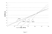
前記インバータの出力電圧の振幅は、整流されてはいるが濾波されていない前記ライン周波数の電圧に比例して変化する。前記インバータ電圧の関数としての前記負荷電流を決定するために、コンピュータによるシミュレーションを行った。ゼロボルトから前記整流後のライン電圧のピーク値までの範囲にわたるインバータの出力電圧の複数の値について、時間領域回路シミュレーションを行った。これに対応する負荷電流が、前記インバータの整流後の正弦波供給電圧の関数として図7にグラフ化されている。 The amplitude of the output voltage of the inverter varies in proportion to the voltage of the line frequency that is rectified but not filtered. A computer simulation was performed to determine the load current as a function of the inverter voltage. A time domain circuit simulation was performed for a plurality of values of the output voltage of the inverter ranging from zero volts to the peak value of the line voltage after rectification. The corresponding load current is graphed in FIG. 7 as a function of the rectified sinusoidal supply voltage of the inverter.
図7に示すように、前記AC電圧源の周波数が前記ネットワークの共振周波数である19kHzに設定されているとき、電池充電電流は線形であり、前記インバータ電源電圧に比例している。電池充電電流の線形性は、負荷が軽いときの共振回路の電圧変換特性に従って、前記電池の開路端子電圧よりもはるかに低いライン電源電圧についてさえ維持できることに留意することが重要である。図7の線形曲線は、2次側負荷電流の望ましい状態を示しており、したがって、インバータ供給電流およびライン電流はライン電圧に比例しており、これは低レベルのライン周波数の高調波歪みおよびライン周波数の力率1を保証する条件である。図7に示したように、前記インピーダンスインバータの共振周波数よりも高いまたは低い17、18、20kHzで動作すると、前記ライン電圧/ライン電流の関係は低いライン電圧ではもはや比例せず、ライン電流に高調波歪みが生じ、ライン力率が劣化する。前記インピーダンスインバータの共振周波数で動作すると、電流は正弦半波、即ち、整流後の正弦波の形状で変化する。 As shown in FIG. 7, when the frequency of the AC voltage source is set to 19 kHz which is the resonant frequency of the network, the battery charging current is linear and proportional to the inverter power supply voltage. It is important to note that the linearity of the battery charging current can be maintained even for line power supply voltages that are much lower than the open circuit terminal voltage of the battery, according to the voltage conversion characteristics of the resonant circuit when the load is light. The linear curve in FIG. 7 shows the desired state of the secondary load current, so the inverter supply current and line current are proportional to the line voltage, which is a low level line frequency harmonic distortion and line. This is a condition for guaranteeing a frequency power factor of 1. As shown in FIG. 7, when operating at 17, 18, 20 kHz higher or lower than the resonant frequency of the impedance inverter, the line voltage / line current relationship is no longer proportional to the lower line voltage and is higher than the line current. Wave distortion occurs and the line power factor deteriorates. When operating at the resonant frequency of the impedance inverter, the current changes in the shape of a sine half wave, that is, a sine wave after rectification.
従来、電池の充電は、電池の充電電流および最大電池電圧、ならびに温度(時には前記電池全体の温度の場合もあるが個別のセルの温度の場合もある)のようなその他の関連パラメータを監視および制御する電池管理システムによって調整される。現行の実施において、電池/セル管理システムはDC充電電流の使用を必要とし、正弦半波の充電電流が存在すると誤動作する可能性が高い。この難点は、前記電池管理システムを、従来より用いられている平均またはピーク測定法の代わりに充電電流の二乗平均平方根に応答するように修正することにより排除される。 Traditionally, battery charging involves monitoring and other related parameters such as battery charging current and maximum battery voltage, and temperature (sometimes the temperature of the entire battery or individual cells). Regulated by the battery management system to control. In current implementations, the battery / cell management system requires the use of DC charging current and is likely to malfunction if a sinusoidal half-wave charging current is present. This difficulty is eliminated by modifying the battery management system to respond to the root mean square charge current instead of the traditional average or peak measurement method.
電池の効果的な充電には、電池充電アルゴリズムが制御する電池の充電状態に従って充電電流の大きさを変更することが必要である。本発明の例示的な実施形態において、電池の最大充電電流の大きさは、前記インピーダンス反転ネットワークの設計および前記インバータ18に供給される整流後の正弦半波のライン電圧の大きさによって設定される。前記インバータ18のパルス幅変調、インバータのパルスの位相調整、インバータのパルス間引き、および前記2次側整流器26の能動的制御によって、電池の充電電流のさらなる制御(低減)が達成される。これらの個別にまたは組み合わせで用いられる制御方法により、高調波歪みを小さく抑えかつほぼ力率1を維持しながら、充電電流の大きさの効果的な制御が可能となる。
Effective charging of the battery requires changing the magnitude of the charging current in accordance with the state of charge of the battery controlled by the battery charging algorithm. In an exemplary embodiment of the invention, the maximum charge current magnitude of the battery is set by the impedance inversion network design and the magnitude of the rectified half-wave line voltage supplied to the
低中度の電力の無線電力システムが単相電力接続によって動作する一方、大電力システムは一般的に3相接続を必要とする。整流後の単相正弦波電源は大きなリップル成分を有するが、各正弦波が120度ずれた3つの整流正弦波電源の総和ははるかに小さい。電池管理システム回路との適合性および高速充電中の電池抵抗損失を制限するためのピーク充電電流対平均充電電流の比の低減のために、充電リップル電流を低減することが、時として望ましい。 While low to medium power wireless power systems operate with a single phase power connection, high power systems typically require a three phase connection. The rectified single-phase sine wave power supply has a large ripple component, but the sum of the three rectified sine wave power supplies with each sine wave shifted by 120 degrees is much smaller. It is sometimes desirable to reduce charge ripple current for compatibility with battery management system circuitry and for reducing the ratio of peak charge current to average charge current to limit battery resistance loss during fast charging.
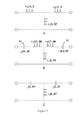
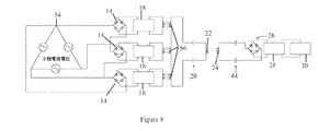
図8は、3相ライン電圧源54を用いて実施される本発明の実施形態を示している。各相は、別個の整流器14とインバータ18とを有している。前記3つのインバータは同期して切り替わり、前記インバータの出力は、3つの物理的に独立した変圧器またはコア材料の効率的な使用を可能とするための共通コア上に3相の部分的な磁束相殺を伴う6つの巻線を有する単一の変圧器であってもよい加算変圧器56によって結合する。前記加算変圧器56はまた、前記ACラインとのガルバニック絶縁をも提供する。前記3相ライン上のフィルタ(図8には図示せず)がインバータのスイッチング周波数成分を排除し、力率1の高調波歪みの小さな新しい3相負荷が生じる。従来技術の図1に示すように、共振ネットワーク20が前記インバータ18を前記1次側誘導コイル22に接続している。1次側誘導コイル22と2次側誘導コイル24との間の電磁結合によって1次側エネルギーが2次側に転送され、高周波整流器26によって整流され、リップルフィルタ28によってリップル濾波され、遠隔配置された電池30を充電するために使用される。共振ネットワーク44が前記2次側誘導コイル24を共振させることにより、最大電流の流れおよび最大エネルギーの転送を可能とする。
FIG. 8 illustrates an embodiment of the present invention implemented using a three-phase
図9は、図8の代替的な実施形態を示しており、前記加算変圧器56が、前記2次側整流器に接続された2次側誘導コイルと共通の磁気コアを共有して共同設置された3つの独立した誘導コイル23として実施された前記1次側誘導コイル22で置き換えられている。別個のDC/ACインバータ18およびこれに関連付けられるライン周波数整流器14が、共振ネットワーク20を介して前記3つの1次側コイルの各々を駆動する。このとき、専用の結合変圧器56が不要となるように、1次側コイルの磁界の加算として、電力の加算が行われる。当業者であれば、図9の実施形態では、2つの1次側コイルおよび2組の共振コンデンサと引き換えに、前記結合変圧器のサイズ、重量、およびコストが削除されることを理解するであろう。
FIG. 9 shows an alternative embodiment of FIG. 8, where the summing
本明細書内で説明したターマン・インピーダンス・インバータ・ネットワークの力率補正作用は、共振誘導無線電力転送システム以外の装置にも都合よく用いることができる。このような用途として、次のものが挙げられる。
無線とは対照的な配線式電池充電、
めっき、
電気分解などの電気化学的処理、
誘導加熱、
交流溶接法
蛍光灯およびアーク照明などのガス放電処理、および
交流源由来の直流を全波整流正弦波直流を許容できる負荷に提供するその他任意の用途。
The power factor correction action of the terman impedance inverter network described herein can be conveniently used for devices other than the resonance induction wireless power transfer system. Examples of such applications include the following.
Wired battery charging as opposed to wireless,
Plating,
Electrochemical treatment such as electrolysis,
Induction heating,
Gas discharge treatments such as AC welding fluorescent lamps and arc lighting, and any other application that provides direct current from an alternating current source to a load that can tolerate full wave rectified sinusoidal direct current.
無線誘導電力転送の力率制御において、前記ターマンインピーダンス反転ネットワークは、相互に連結された空心コイル対の前記無線転送のT型等価回路の一部であり、前記T型等価回路の1要素は、前記相互インダクタンスである。当業者であれば、無線電力転送以外の用途において、前記インピーダンス反転ネットワークは、設計の自由度を著しく向上させる、相互に連結していない3つの個別の構成要素で実施することができることを理解するであろう。 In power factor control of wireless inductive power transfer, the terminator impedance reversal network is a part of the wireless transfer T-type equivalent circuit of interconnected air-core coils, and one element of the T-type equivalent circuit is: The mutual inductance. One skilled in the art will appreciate that in applications other than wireless power transfer, the impedance reversal network can be implemented with three separate components that are not interconnected, significantly improving design freedom. Will.
上述の用途において、電力は、前記AC源にほぼ力率1の負荷を提供する装置によりAC源からDC負荷へと流れる。本発明の教示は、この代わりに、ほぼ力率1のAC源を提供する装置によりDC源からAC負荷へと反対方向に電力が流れる用途にも等しく当てはまる。電力の流れが反転している装置には、光起電力パネルおよび風力発電機のような代替エネルギー源からのDC電力を50Hzまたは60Hzの電力系統に供給するインバータとしての用途がある。 In the applications described above, power flows from the AC source to the DC load by a device that provides a load of approximately unity power factor to the AC source. The teachings of the present invention are equally applicable to applications in which power is supplied in the opposite direction from a DC source to an AC load by means of an apparatus that provides an approximately one power factor AC source instead. Devices with reversed power flow have applications as inverters that supply DC power from alternative energy sources, such as photovoltaic panels and wind power generators, to 50 or 60 Hz power systems.
図10は、この代わりに、ほぼ力率1のAC源を提供する装置によってDC源からAC負荷へと反対方向に電力が流れる用途に有用なDC/ACインバータシステムに関する概念ブロック図およびこれに関連付けられる電圧波形を図示している。図示のように、図10の回路は、DC電源60に続いてライン周波数のリップルを濾波するシャント・リップル・フィルタ・コンデンサ62を含んでいる。前記ライン周波数のリップルを濾波したDC電圧が、高周波DC/ACインバータ64に印加されている。この文脈における高周波とは、前記ライン周波数に対して高いことを意味する。前記インピーダンス反転ネットワークの遠位側における前記瞬時負荷電圧によって変化する変圧を提供するターマンインピーダンス反転ネットワーク68の入力に、前記方形波出力電圧66が印加されている。
FIG. 10 is a conceptual block diagram and association associated with a DC / AC inverter system useful in applications where power flows in the opposite direction from the DC source to the AC load by an apparatus that provides an AC source of approximately power factor instead. The voltage waveform which is obtained is illustrated. As shown, the circuit of FIG. 10 includes a
前記インピーダンス反転ネットワーク68の出力における波形70は、ライン周波数の正弦波によって包絡線変調された、DC/ACインバータ周波数の正弦波である。高周波整流器72が、前記双極正弦波包絡線を単極の正弦半波包絡線74に変換する。高周波リップル・フィルタ・ネットワーク76が、前記高周波リップルを除去し、リップルのないライン周波数の正弦半波の波形78を与える。半波ブリッジまたは全波ブリッジに構成された電力半導体スイッチを含む整流戻しネットワーク80が、波形78の1つおきの周期の極性を反転させて波形82を発生させることにより、無限格子を表す前記AC定電圧負荷84に電力が流れることを可能とする。
The waveform 70 at the output of the
各ストリングが絶縁変圧器90を追加した単相インバータストリングと同様である3つの独立したDC/ACインバータストリングを用いて、図11に示す3相AC系統負荷が提供される。各ストリングが、全体としてAC3相定電圧負荷92を構成する3つの前記AC定電圧負荷のうちの1個を駆動する。絶縁変圧器90が、前記AC負荷92とのガルバニック絶縁を提供する。DC源94は、3つの独立した等電圧の図10に示すようなDC源であってもよく、または前記3つのDC源ノードを束ねて単一DC源によって供給してもよい。フィルタコンデンサ96が、さもなくば前記DC源ノードに存在することとなるであろう前記120Hzの正弦半波の電流変動を濾波する。前記要素および動作は、それ以外の点においては図10の回路構成と同様である。
The three-phase AC grid load shown in FIG. 11 is provided using three independent DC / AC inverter strings, each string being similar to a single-phase inverter string with the addition of an
当業者であれば、本発明が無線電力装置の用途に限定されないことを理解するであろう。本発明はまた、無線誘導充電用途に加え、AC誘導モーター、モーターコントローラ、共振型電源、産業用誘導加熱、融解、はんだ付け、表面硬化装置、溶接装置、電源変圧器、電子商品監視装置、誘導調理機器およびレンジ、その他の産業用機器、ならびにプラグイン充電器によるプラグイン充電を組み込んだその他の用途などの輸送産業以外への使用、ならびに電気化学、電気めっきおよび単相電源電圧からの正弦半波電流波形または多相電源電圧の総和の結果得られるリップル低減波形で動作することのできるその他すべての負荷などの電池充電以外のその他の用途に適用することもできる。これらおよびその他の実施形態は、以下の請求項によって定義される本発明の範囲内に含まれるとみなされる。 One skilled in the art will appreciate that the present invention is not limited to wireless power device applications. In addition to wireless induction charging applications, the present invention also provides AC induction motors, motor controllers, resonant power supplies, industrial induction heating, melting, soldering, surface hardening devices, welding devices, power transformers, electronic merchandise monitoring devices, induction Non-transport industry use such as cooking equipment and ranges, other industrial equipment, and other applications incorporating plug-in charging with plug-in chargers, and half-sine from electrochemical, electroplating and single-phase power supply voltages It can also be applied to other uses other than battery charging, such as all other loads that can operate with wave current waveforms or ripple reduced waveforms resulting from the sum of multiphase power supply voltages. These and other embodiments are considered to be within the scope of the invention as defined by the following claims.
Claims (18)
AC電源電圧と、
前記AC電源電圧に接続され、正弦半波整流供給電圧(half−sinusoidal rectified supply voltage)を提供するライン周波数整流器と、
前記正弦半波整流供給電圧に応答してインピーダンス反転した(impedance inverted)2次側電圧を出力に提供するインピーダンスインバータと、
前記2次側電圧を整流する2次側整流器と、
前記2次側整流器から供給される整流後出力を濾波してインバータ周波数のリップルを除去し、ライン周波数の正弦半波電流を出力に供給する2次側リップルフィルタと、
前記ライン周波数の正弦半波電流を受け取る負荷と、
を有し、
前記インピーダンスインバータは、軽負荷条件下において前記2次側電圧を上昇させることにより、前記AC電源電圧から供給されるライン周波数の電源電流および前記負荷における前記ライン周波数の正弦半波電流を比例させてほぼ力率1のライン負荷力率を維持し、高調波電流の歪みを小さく抑えるものである
装置。 An intrinsic power factor correction device,
AC power supply voltage,
A line frequency rectifier connected to the AC power supply voltage and providing a half-sinusoidally rectified supply voltage;
An impedance inverter that provides an impedance inverted secondary voltage to the output in response to the sine half-wave rectified supply voltage;
A secondary rectifier for rectifying the secondary voltage;
A secondary ripple filter that filters the rectified output supplied from the secondary rectifier to remove the inverter frequency ripple and supplies a sine half wave current of the line frequency to the output;
A load receiving a sine half-wave current of the line frequency;
Have
The impedance inverter increases the secondary voltage under light load conditions, thereby proportionally supplying the line frequency power supply current supplied from the AC power supply voltage and the line frequency sine half-wave current in the load. A device that maintains a line load power factor of approximately 1 and keeps harmonic current distortion small.
前記3相のACライン上に伝送周波数インバータのスイッチング周波数成分を排除するフィルタを有するものである装置。 The apparatus of claim 3, further comprising:
An apparatus having a filter for eliminating a switching frequency component of a transmission frequency inverter on the three-phase AC line.
DC電源と、
前記DC電源の出力のライン周波数のリップルを濾波するシャント・リップル・フィルタ・コンデンサと、
前記シャント・リップル・フィルタ・コンデンサの出力から供給されるライン周波数のリップルを濾波したDC電圧を出力方形波電圧に変換するDC/ACインバータと、
前記出力方形波電圧を、ライン周波数の正弦波によって包絡線変調された、DC/ACコンバータの周波数の正弦波に変換して双極正弦波包絡線を形成するインピーダンスインバータと、
前記双極正弦波包絡線を単極正弦半波包絡線に整流する2次側整流器と、
前記単極正弦半波における1つおきの周期の極性を反転させて正弦波形を発生させる整流戻し(de−rectification)ネットワークと、
前記正弦波形を受け取るAC負荷と
を有し、
前記インピーダンスインバータは、軽負荷条件下において2次側電圧を上昇させることにより、前記DC電源から供給されるライン周波数の電源電流および前記AC負荷における電流を比例させてほぼ力率1のライン負荷力率を維持し、高調波電流の歪みを小さく抑えるものである
装置。 An intrinsic power factor correction device,
A DC power supply;
A shunt ripple filter capacitor for filtering the line frequency ripple at the output of the DC power supply;
A DC / AC inverter for converting a DC voltage obtained by filtering a ripple of a line frequency supplied from an output of the shunt ripple filter capacitor into an output square wave voltage;
An impedance inverter that converts the output square wave voltage into a sine wave at the frequency of a DC / AC converter that is envelope modulated by a sine wave at a line frequency to form a bipolar sine wave envelope;
A secondary rectifier for rectifying the bipolar sine wave envelope into a monopolar sine half wave envelope;
A de-rectification network that inverts the polarity of every other period in the unipolar sine half wave to generate a sine waveform;
An AC load that receives the sinusoidal waveform;
The impedance inverter raises the secondary voltage under light load conditions, thereby making the line frequency power supply current supplied from the DC power supply proportional to the current in the AC load, and a line load force having a power factor of approximately 1. A device that maintains the rate and suppresses distortion of harmonic currents.
前記単極正弦半波包絡線が前記整流戻しネットワークに印加される前に前記単極正弦半波包絡線から高周波リップルを除去するリップル・フィルタ・ネットワークを有するものである装置。 The apparatus of claim 12, further comprising:
An apparatus comprising a ripple filter network that removes high frequency ripple from the unipolar sine half wave envelope before the unipolar sine half wave envelope is applied to the rectified return network.
前記DC電源と前記AC負荷との間にガルバニック絶縁を提供する絶縁変圧器を有するものである装置。 The apparatus of claim 12, further comprising:
An apparatus comprising an isolation transformer that provides galvanic isolation between the DC power source and the AC load.
Applications Claiming Priority (3)
| Application Number | Priority Date | Filing Date | Title |
|---|---|---|---|
| US201462065889P | 2014-10-20 | 2014-10-20 | |
| US62/065,889 | 2014-10-20 | ||
| PCT/US2015/056204 WO2016064725A1 (en) | 2014-10-20 | 2015-10-19 | Method and apparatus for intrinsic power factor correction |
Publications (2)
| Publication Number | Publication Date |
|---|---|
| JP2017532943A true JP2017532943A (en) | 2017-11-02 |
| JP2017532943A5 JP2017532943A5 (en) | 2018-11-15 |
Family
ID=55761362
Family Applications (1)
| Application Number | Title | Priority Date | Filing Date |
|---|---|---|---|
| JP2017521091A Pending JP2017532943A (en) | 2014-10-20 | 2015-10-19 | Intrinsic power factor correction method and apparatus |
Country Status (9)
| Country | Link |
|---|---|
| US (1) | US20170237340A1 (en) |
| EP (1) | EP3210295A4 (en) |
| JP (1) | JP2017532943A (en) |
| KR (1) | KR20170071587A (en) |
| CN (1) | CN107112912A (en) |
| CA (1) | CA2964326A1 (en) |
| HK (1) | HK1243560A1 (en) |
| MX (1) | MX2017005100A (en) |
| WO (1) | WO2016064725A1 (en) |
Families Citing this family (26)
| Publication number | Priority date | Publication date | Assignee | Title |
|---|---|---|---|---|
| US9991779B2 (en) * | 2014-01-07 | 2018-06-05 | NuVolta Technologies | Harmonic reduction apparatus for wireless power transfer systems |
| DE102014019621A1 (en) * | 2014-12-29 | 2016-06-30 | Markus Rehm | Coupling optimized electrical wireless power transmission |
| US20160336784A1 (en) * | 2015-05-15 | 2016-11-17 | Intel Corporation | Reconfigrable charging station for extended power capability and active area |
| US10361586B2 (en) * | 2015-12-29 | 2019-07-23 | Motorola Solutions, Inc. | Method of wirelessly transferring power |
| KR102154251B1 (en) | 2016-10-11 | 2020-09-09 | 주식회사 아모센스 | Electromagnetic inductive power supply apparatus |
| KR102030721B1 (en) | 2016-10-19 | 2019-10-10 | 주식회사 아모센스 | Electromagnetic inductive power supply apparatus |
| CN106685233B (en) * | 2017-01-12 | 2019-04-05 | 南京矽力杰半导体技术有限公司 | Passive boost network and the DC-DC boost converter for applying it |
| CN107144807A (en) * | 2017-07-20 | 2017-09-08 | 云南电网有限责任公司电力科学研究院 | GIS current transformer verifying power supplies based on phase-shifting carrier wave multiple technology |
| CN108023479A (en) * | 2017-11-28 | 2018-05-11 | 李建廷 | A kind of power converter circuit |
| WO2019130874A1 (en) * | 2017-12-27 | 2019-07-04 | 株式会社村田製作所 | Power supply device |
| KR102524188B1 (en) * | 2018-04-03 | 2023-04-21 | 현대자동차주식회사 | Battery charger for electric vehicle |
| US10797506B2 (en) | 2018-04-05 | 2020-10-06 | Witricity Corporation | DC to AC power conversion using a wireless power receiver |
| CN108695960A (en) * | 2018-04-27 | 2018-10-23 | 武汉中智德远科技开发有限公司 | A kind of voltage-stabilizing and energy-saving charge controller |
| CN109271732B (en) * | 2018-09-30 | 2023-04-07 | 浙江中创天成科技有限公司 | Modeling method of electric automobile dynamic wireless charging system |
| KR20200071286A (en) | 2018-12-11 | 2020-06-19 | 삼성전자주식회사 | Wireless power receiver |
| CN109515220A (en) * | 2018-12-16 | 2019-03-26 | 中国电建集团华东勘测设计研究院有限公司 | A kind of wireless charging device and wireless charging method applied to the double loads of electric car |
| US11631998B2 (en) * | 2019-01-10 | 2023-04-18 | Hengchun Mao | High performance wireless power transfer and power conversion technologies |
| CN110061570B (en) * | 2019-05-28 | 2020-10-02 | 浙江大学 | Wireless power transmission system for realizing PFC (Power factor correction) through secondary modulation |
| US11784503B2 (en) | 2021-02-22 | 2023-10-10 | Inductev Inc. | Passive arc detection and mitigation in wireless power transfer system |
| CN112711329B (en) * | 2020-12-25 | 2022-05-27 | 瑞声新能源发展(常州)有限公司科教城分公司 | Vibrator driving method and system, and storage medium of vibration driving device |
| CN113162453B (en) * | 2021-04-20 | 2022-11-29 | 哈尔滨工业大学 | High-frequency inversion system and control method |
| KR20230045247A (en) * | 2021-09-28 | 2023-04-04 | 삼성전자주식회사 | Wireless power transmitter comprising an impedance matching circuit and method for transmitting a wireless power |
| CN114070035B (en) * | 2021-11-12 | 2023-12-26 | 上海联影医疗科技股份有限公司 | Power supply device and medical equipment |
| CN114069882B (en) * | 2021-11-16 | 2024-01-30 | 华东交通大学 | Self-powered low-voltage power supply system of high-voltage power cable and control method thereof |
| CN115730427B (en) * | 2022-10-31 | 2024-04-09 | 国网江苏省电力有限公司苏州供电分公司 | Circuit electrical parameter estimation method and system based on electromagnetic field domain calculation |
| CN115864615A (en) * | 2023-02-15 | 2023-03-28 | 小神童创新科技(广州)有限公司 | Full-bridge LLC soft switch resonant charger with power factor correction function and control method |
Citations (4)
| Publication number | Priority date | Publication date | Assignee | Title |
|---|---|---|---|---|
| JPH09117151A (en) * | 1995-10-16 | 1997-05-02 | Sharp Corp | Inverter control method and device |
| JP2001103685A (en) * | 1999-08-02 | 2001-04-13 | General Motors Corp <Gm> | Power factor correction type single step induction charger |
| JP2002095241A (en) * | 2000-09-14 | 2002-03-29 | Toshihisa Shimizu | Immitance conversion circuit and converter using it |
| JP2007181162A (en) * | 2005-12-28 | 2007-07-12 | Juichi Irie | Immittance transducer |
Family Cites Families (13)
| Publication number | Priority date | Publication date | Assignee | Title |
|---|---|---|---|---|
| US3704433A (en) * | 1971-05-27 | 1972-11-28 | Bell Telephone Labor Inc | Band-elimination filter |
| US3792286A (en) * | 1971-10-12 | 1974-02-12 | Reliance Electric Co | Combining inverters for harmonic reduction |
| US4916380A (en) * | 1989-02-27 | 1990-04-10 | Honeywell Inc. | Regulated switching power supply with complex output filter |
| US4992723A (en) * | 1989-03-31 | 1991-02-12 | Square D Company | Fault-powered power supply |
| US7679943B2 (en) * | 2007-01-08 | 2010-03-16 | Maxvision Corporation | Uninterruptable power supply |
| US8159802B2 (en) * | 2008-11-17 | 2012-04-17 | Lockheed Martin Corporation | 3-phase power factor corrected AC to DC filtered switching power supply |
| US8923015B2 (en) * | 2008-11-26 | 2014-12-30 | Auckland Uniservices Limited | Primary-side power control for inductive power transfer |
| US8384371B2 (en) * | 2009-12-18 | 2013-02-26 | Rosendin Electric, Inc. | Various methods and apparatuses for an integrated zig-zag transformer |
| WO2012062375A1 (en) * | 2010-11-12 | 2012-05-18 | Sma Solar Technology Ag | Power inverter for feeding electric energy from a dc power generator into an ac grid with two power lines |
| JP5927826B2 (en) * | 2011-09-28 | 2016-06-01 | 日産自動車株式会社 | Contactless power supply |
| DE102011116057A1 (en) * | 2011-10-18 | 2013-04-18 | Paul Vahle Gmbh & Co. Kg | Network simulation in the secondary circuit of non-contact energy transmission |
| WO2013085522A1 (en) * | 2011-12-08 | 2013-06-13 | Petra Solar, Inc. | Secondary side cycloconverter drive circuit for resonant coverter in solar application |
| CN102969776B (en) * | 2012-12-03 | 2014-12-10 | 中国科学院电工研究所 | Wireless charging device of electronic automobile |
-
2015
- 2015-10-19 EP EP15853529.4A patent/EP3210295A4/en not_active Withdrawn
- 2015-10-19 CA CA2964326A patent/CA2964326A1/en not_active Abandoned
- 2015-10-19 US US15/518,675 patent/US20170237340A1/en not_active Abandoned
- 2015-10-19 JP JP2017521091A patent/JP2017532943A/en active Pending
- 2015-10-19 KR KR1020177013601A patent/KR20170071587A/en unknown
- 2015-10-19 WO PCT/US2015/056204 patent/WO2016064725A1/en active Application Filing
- 2015-10-19 CN CN201580056611.0A patent/CN107112912A/en active Pending
- 2015-10-19 MX MX2017005100A patent/MX2017005100A/en unknown
-
2018
- 2018-02-27 HK HK18102774.8A patent/HK1243560A1/en unknown
Patent Citations (4)
| Publication number | Priority date | Publication date | Assignee | Title |
|---|---|---|---|---|
| JPH09117151A (en) * | 1995-10-16 | 1997-05-02 | Sharp Corp | Inverter control method and device |
| JP2001103685A (en) * | 1999-08-02 | 2001-04-13 | General Motors Corp <Gm> | Power factor correction type single step induction charger |
| JP2002095241A (en) * | 2000-09-14 | 2002-03-29 | Toshihisa Shimizu | Immitance conversion circuit and converter using it |
| JP2007181162A (en) * | 2005-12-28 | 2007-07-12 | Juichi Irie | Immittance transducer |
Also Published As
| Publication number | Publication date |
|---|---|
| MX2017005100A (en) | 2017-06-20 |
| US20170237340A1 (en) | 2017-08-17 |
| CA2964326A1 (en) | 2016-04-28 |
| EP3210295A1 (en) | 2017-08-30 |
| HK1243560A1 (en) | 2018-07-13 |
| KR20170071587A (en) | 2017-06-23 |
| EP3210295A4 (en) | 2018-05-23 |
| CN107112912A (en) | 2017-08-29 |
| WO2016064725A1 (en) | 2016-04-28 |
Similar Documents
| Publication | Publication Date | Title |
|---|---|---|
| JP2017532943A (en) | Intrinsic power factor correction method and apparatus | |
| Aditya et al. | A review of optimal conditions for achieving maximum power output and maximum efficiency for a series–series resonant inductive link | |
| Bac et al. | A SiC-based matrix converter topology for inductive power transfer system | |
| US7724549B2 (en) | Integrated power conditioning system and housing for delivering operational power to a motor | |
| AU2015100179A4 (en) | A battery charger with power factor correction | |
| CN105874701B (en) | High frequency serial AC voltage regulator | |
| JP2017532943A5 (en) | ||
| Liu et al. | Hybrid frequency pacing for high-order transformed wireless power transfer | |
| EP3038246A2 (en) | Dc-ac conversion circuit topologie | |
| CN110945770A (en) | DC coupling electric converter | |
| Suresh et al. | Review on harmonics and its eliminating strategies in power system | |
| Kalpana et al. | Harmonic mitigator based on 12-pulse ac–dc converter for switched mode power supply | |
| US5587892A (en) | Multi-phase power converter with harmonic neutralization | |
| KR20190115364A (en) | Single and three phase combined charger | |
| US5625543A (en) | Power converter with harmonic neutralization | |
| Asa et al. | Efficiency analysis of a Bi-directional DC/DC converter for wireless energy transfer applications | |
| Khodabandeh et al. | A highly reliable single-phase AC to three-phase AC converter with a small link capacitor | |
| JP6397481B2 (en) | Electronic sine wave transformer | |
| JP2022543904A (en) | Vehicle-Grid-Home Power Interface | |
| Liu et al. | A compact power converter for high current and low voltage applications | |
| WO2016132471A1 (en) | Power conversion device and initial charging method therefor | |
| Zhong et al. | Power factor correction modulated wireless power transfer system with series-series compensation | |
| Samanta et al. | Medium voltage supply directly to data-center-servers using SiC-based single-stage converter with 20kW experimental results | |
| Flayyih et al. | A novel hybrid votage-current fed induction heating power supply system using multilevel neutral point clamped inverter | |
| RU2558681C1 (en) | Independent voltage inverter to supply load through transformer with low coupling coefficient between its windings |
Legal Events
| Date | Code | Title | Description |
|---|---|---|---|
| A521 | Request for written amendment filed |
Free format text: JAPANESE INTERMEDIATE CODE: A523 Effective date: 20181004 |
|
| A621 | Written request for application examination |
Free format text: JAPANESE INTERMEDIATE CODE: A621 Effective date: 20181004 |
|
| A977 | Report on retrieval |
Free format text: JAPANESE INTERMEDIATE CODE: A971007 Effective date: 20190814 |
|
| A131 | Notification of reasons for refusal |
Free format text: JAPANESE INTERMEDIATE CODE: A131 Effective date: 20190924 |
|
| A02 | Decision of refusal |
Free format text: JAPANESE INTERMEDIATE CODE: A02 Effective date: 20200707 |