JP2017519902A - Installation and insulation of radio frequency identification devices (RFIDs) in metals for sputtering targets - Google Patents
Installation and insulation of radio frequency identification devices (RFIDs) in metals for sputtering targets Download PDFInfo
- Publication number
- JP2017519902A JP2017519902A JP2016569883A JP2016569883A JP2017519902A JP 2017519902 A JP2017519902 A JP 2017519902A JP 2016569883 A JP2016569883 A JP 2016569883A JP 2016569883 A JP2016569883 A JP 2016569883A JP 2017519902 A JP2017519902 A JP 2017519902A
- Authority
- JP
- Japan
- Prior art keywords
- plug
- backing plate
- hole
- composite
- alloy
- Prior art date
- Legal status (The legal status is an assumption and is not a legal conclusion. Google has not performed a legal analysis and makes no representation as to the accuracy of the status listed.)
- Pending
Links
Images
Classifications
-
- H—ELECTRICITY
- H01—ELECTRIC ELEMENTS
- H01J—ELECTRIC DISCHARGE TUBES OR DISCHARGE LAMPS
- H01J37/00—Discharge tubes with provision for introducing objects or material to be exposed to the discharge, e.g. for the purpose of examination or processing thereof
- H01J37/32—Gas-filled discharge tubes
- H01J37/32917—Plasma diagnostics
- H01J37/32935—Monitoring and controlling tubes by information coming from the object and/or discharge
-
- C—CHEMISTRY; METALLURGY
- C23—COATING METALLIC MATERIAL; COATING MATERIAL WITH METALLIC MATERIAL; CHEMICAL SURFACE TREATMENT; DIFFUSION TREATMENT OF METALLIC MATERIAL; COATING BY VACUUM EVAPORATION, BY SPUTTERING, BY ION IMPLANTATION OR BY CHEMICAL VAPOUR DEPOSITION, IN GENERAL; INHIBITING CORROSION OF METALLIC MATERIAL OR INCRUSTATION IN GENERAL
- C23C—COATING METALLIC MATERIAL; COATING MATERIAL WITH METALLIC MATERIAL; SURFACE TREATMENT OF METALLIC MATERIAL BY DIFFUSION INTO THE SURFACE, BY CHEMICAL CONVERSION OR SUBSTITUTION; COATING BY VACUUM EVAPORATION, BY SPUTTERING, BY ION IMPLANTATION OR BY CHEMICAL VAPOUR DEPOSITION, IN GENERAL
- C23C14/00—Coating by vacuum evaporation, by sputtering or by ion implantation of the coating forming material
- C23C14/22—Coating by vacuum evaporation, by sputtering or by ion implantation of the coating forming material characterised by the process of coating
- C23C14/34—Sputtering
- C23C14/3407—Cathode assembly for sputtering apparatus, e.g. Target
-
- G—PHYSICS
- G06—COMPUTING OR CALCULATING; COUNTING
- G06K—GRAPHICAL DATA READING; PRESENTATION OF DATA; RECORD CARRIERS; HANDLING RECORD CARRIERS
- G06K19/00—Record carriers for use with machines and with at least a part designed to carry digital markings
- G06K19/06—Record carriers for use with machines and with at least a part designed to carry digital markings characterised by the kind of the digital marking, e.g. shape, nature, code
- G06K19/067—Record carriers with conductive marks, printed circuits or semiconductor circuit elements, e.g. credit or identity cards also with resonating or responding marks without active components
- G06K19/07—Record carriers with conductive marks, printed circuits or semiconductor circuit elements, e.g. credit or identity cards also with resonating or responding marks without active components with integrated circuit chips
- G06K19/077—Constructional details, e.g. mounting of circuits in the carrier
- G06K19/07749—Constructional details, e.g. mounting of circuits in the carrier the record carrier being capable of non-contact communication, e.g. constructional details of the antenna of a non-contact smart card
-
- H—ELECTRICITY
- H01—ELECTRIC ELEMENTS
- H01J—ELECTRIC DISCHARGE TUBES OR DISCHARGE LAMPS
- H01J37/00—Discharge tubes with provision for introducing objects or material to be exposed to the discharge, e.g. for the purpose of examination or processing thereof
- H01J37/32—Gas-filled discharge tubes
- H01J37/34—Gas-filled discharge tubes operating with cathodic sputtering
- H01J37/3402—Gas-filled discharge tubes operating with cathodic sputtering using supplementary magnetic fields
- H01J37/3405—Magnetron sputtering
-
- H—ELECTRICITY
- H01—ELECTRIC ELEMENTS
- H01J—ELECTRIC DISCHARGE TUBES OR DISCHARGE LAMPS
- H01J37/00—Discharge tubes with provision for introducing objects or material to be exposed to the discharge, e.g. for the purpose of examination or processing thereof
- H01J37/32—Gas-filled discharge tubes
- H01J37/34—Gas-filled discharge tubes operating with cathodic sputtering
- H01J37/3411—Constructional aspects of the reactor
- H01J37/3414—Targets
- H01J37/3417—Arrangements
Landscapes
- Chemical & Material Sciences (AREA)
- Engineering & Computer Science (AREA)
- Physics & Mathematics (AREA)
- Plasma & Fusion (AREA)
- Analytical Chemistry (AREA)
- Materials Engineering (AREA)
- Chemical Kinetics & Catalysis (AREA)
- Mechanical Engineering (AREA)
- Metallurgy (AREA)
- Organic Chemistry (AREA)
- Computer Hardware Design (AREA)
- Microelectronics & Electronic Packaging (AREA)
- General Physics & Mathematics (AREA)
- Theoretical Computer Science (AREA)
- Physical Vapour Deposition (AREA)
Abstract
スパッタ・ターゲット/バッキング・プレート組立体のためのRFIDタグ格納複合体。穴は、ターゲットとバッキング・プレートのいずれかに設けられて、栓の密着収容に適応している。栓は、RFIDタグを中に支承するように構成された凹状部分を含む。【選択図】 図1RFID tag storage complex for sputter target / backing plate assembly. The hole is provided in either the target or the backing plate, and is adapted to tightly accommodate the stopper. The plug includes a concave portion configured to support the RFID tag therein. [Selection] Figure 1
Description
関連出願の相互参照
本出願は、2014年5月30日出願の米国仮特許出願番号第62/004,939号と2014年12月16日出願の米国仮特許出願第62/092,419号の優先権の利益を享受する。
This application is related to US Provisional Patent Application No. 62 / 004,939 filed May 30, 2014 and US Provisional Patent Application No. 62 / 092,419 filed December 16, 2014. Enjoy the benefits of priority.
本発明は、スパッタ・ターゲット(sputter target)/バッキング・プレート(backing plate)組立体(assembly)に関するが、栓(plug)及びこれに対応する穴(bore)によって、当該ターゲットあるいは当該バッキング・プレートのいずれかに埋め込まれるRFIDタグ(RFID tag)を備えており、RFID読取器(RFID reader)との読取り/書込み通信のため、当該チップを正確に位置決めするように構成されている。 The present invention relates to a sputter target / backing plate assembly, but by means of a plug and a corresponding bore, the target or the backing plate may be An RFID tag embedded in one of the RFID tags is provided, and the chip is accurately positioned for read / write communication with an RFID reader.
無線周波数識別(radio frequency identification: RFID)技術は、多様な環境で使用されて、多様な物品の無線自動識別装置及び機能を提供する。RFIDシステムは一般的に、識別される物品または装置に取り付けられる「タグ(tag)」と呼ばれるトランスポンダー(transponder)あるいは応答器と、当該トランスポンダーと通信する「タグ」読取器(tag reader)と、を含む。 Radio frequency identification (RFID) technology is used in a variety of environments to provide wireless automatic identification devices and functions for a variety of items. RFID systems generally include a transponder or responder called a “tag” that is attached to the item or device to be identified, and a “tag” reader that communicates with the transponder. Including.
多くの場合、タグまたはトランスポンダーは、アンテナを介してRFタグ読取器によって当該トランスポンダーに送信されてきたワイヤレス質問信号(a wireless interrogation signal)に応答する。この応答がコンピュータへ転送されて、当該応答は使用可能なフォーマットに変換される。 Often, a tag or transponder responds to a wireless interrogation signal that has been transmitted to the transponder by an RF tag reader via an antenna. This response is transferred to the computer and the response is converted to a usable format.
スパッタ被覆法または物理的成膜法は、多様な基板の上に材料薄層の付着に広く使用されている。基本的に、このプロセスは、基板上の薄膜または薄層として付着される材料で形成される面を有するスパッタ・ターゲットへのガス・イオン照射を必要とする。ターゲットへのイオン照射により、スパッタされるターゲット材料の原子または分子が生ずるばかりでなく、ターゲットにかなりの熱エネルギーが付与される。ターゲットとの熱交換関係で配置されている熱伝導バッキング・プレートの真下または周囲を一般的に循環する冷却流体の使用により、この熱が放散される。 Sputter coating or physical deposition methods are widely used for the deposition of thin material layers on a variety of substrates. Basically, this process requires gas ion irradiation onto a sputter target having a surface formed of a material deposited as a thin film or thin layer on a substrate. Ion bombardment of the target not only generates atoms or molecules of the target material to be sputtered, but also imparts significant thermal energy to the target. This heat is dissipated through the use of a cooling fluid that typically circulates directly under or around the heat-conducting backing plate that is placed in heat exchange relationship with the target.
カソード組立体(cathode assembly)は、付着面で真空室(evacuated chamber)と接し、その対向面で冷却水と接している。各表面は、セラミック・リングによって圧縮されてシールを完成させるOリングを有する必要がある。これらのシールはカソード組立体の性能にとって不可欠であるので、カソード組立体への追加特徴はこれらのシールを低下させてはならない。 The cathode assembly is in contact with the evacuated chamber at the attachment surface and in contact with the cooling water at the opposite surface. Each surface must have an O-ring that is compressed by a ceramic ring to complete the seal. Because these seals are critical to the performance of the cathode assembly, additional features to the cathode assembly should not degrade these seals.
ターゲットは、不活性ガス、好ましくはアルゴンを含有する真空室にアノードとともに載置されるカソード組立体の一部を形成する。カソード及びアノードには高圧電界が印加される。カソードから噴射された電子との衝突により、不活性ガスがイオン化される。正電荷のガス・イオンがカソードに誘引され、ターゲット表面との衝突時にターゲット材料を放散する。放散されたターゲット材料は、真空容器(evacuated enclosure)を横切って、普通はアノードに近接している所望の基板の上に薄膜として付着する。 The target forms part of a cathode assembly that is mounted with the anode in a vacuum chamber containing an inert gas, preferably argon. A high voltage electric field is applied to the cathode and the anode. The inert gas is ionized by collision with electrons ejected from the cathode. Positively charged gas ions are attracted to the cathode and dissipate the target material upon impact with the target surface. The diffused target material is deposited as a thin film across the evacuated enclosure and on the desired substrate, usually in close proximity to the anode.
典型的なターゲット・カソード組立体では、非磁性バッキング・プレートにターゲットが装着される。ターゲットへのイオン照射により発生される熱を取り除くように、バッキング・プレートは普通、水冷される。ターゲットの露出面の周囲に延在するループまたはトンネルの形の磁界を形成するために、磁石は、典型的には、周知の配置でバッキング・プレートの直下に配設される。 In a typical target-cathode assembly, the target is mounted on a non-magnetic backing plate. The backing plate is usually water cooled to remove the heat generated by ion irradiation of the target. In order to create a magnetic field in the form of a loop or tunnel that extends around the exposed surface of the target, the magnet is typically disposed directly under the backing plate in a known arrangement.
過去においては、ターゲットのフランジ部分の近くにタグまたはチップを封入するためにエポキシを利用して、RFIDタグが接着されていた。これらのエポキシ構造を設けるのは手作業工程で行われていたため、側壁からチップまでの距離は不均一となり、複数の組立体の間で均一な最適化は行われなかった。さらに、エポキシの配合は変動し、気泡を含有することが多く、RF信号の受信及び送信に悪影響を与えていた。 In the past, RFID tags have been bonded using epoxy to enclose the tag or chip near the flange portion of the target. Since these epoxy structures were provided by a manual process, the distance from the side wall to the chip became non-uniform, and uniform optimization was not performed among a plurality of assemblies. In addition, epoxy formulations varied and often contained bubbles, adversely affecting the reception and transmission of RF signals.
一つの例示的実施形態においては、RFIDタグが組立体に埋め込まれるタイプのものとして、スパッタ・ターゲット/バッキング・プレート組立体が提供される。そのため、バッキング・プレートまたはスパッタ・ターゲットの一方に形成された穴と、穴への密着挿入に適した栓とを含む格納複合体(containment combination)が示されている。栓は、外面と凹状部分(recessed part)とを含む。栓の凹状部分の少なくとも一部分と境界を接する栓の中実部が設けられている。栓の凹状部分は、RFIDタグを中に確実に収容するように構成されている。Oリングは、RFIDタグが穴に収容された時に、栓を密封する。 In one exemplary embodiment, a sputter target / backing plate assembly is provided that is of the type in which RFID tags are embedded in the assembly. Thus, a containment combination is shown that includes a hole formed in one of the backing plate or sputter target and a plug suitable for tight insertion into the hole. The plug includes an outer surface and a recessed part. A solid portion of the plug is provided that borders at least a portion of the concave portion of the plug. The concave portion of the stopper is configured to securely accommodate the RFID tag therein. The O-ring seals the plug when the RFID tag is received in the hole.
他の例示的実施形態において、バッキング・プレートまたはターゲットの穴は、Oリングが圧縮されて真空シールまたは水密シールを形成するように求められている。表面の一方に単に装着されるRFIDタグは、適切なシールを形成できない。 In other exemplary embodiments, the backing plate or target hole is required such that the O-ring is compressed to form a vacuum or watertight seal. RFID tags that are simply attached to one of the surfaces cannot form a suitable seal.
他の例示的実施形態においては、バッキング・プレートの表面部分の周囲に沿って穴が配置されている。場合によっては、バッキング・プレートのこの表面は、冷却水の衝突に適したバッキング・プレートの裏側または水側に設けられている。 In other exemplary embodiments, holes are disposed around the periphery of the surface portion of the backing plate. In some cases, this surface of the backing plate is provided on the back or water side of the backing plate suitable for cooling water impingement.
他の実施形態においては、栓及びOリングはわずかな変位を可能にしている。場合によっては、真空シールと水密シールのいずれかに有効なシールを形成するのに、これは不可欠であろう。 In other embodiments, the plug and O-ring allow for slight displacement. In some cases, this may be essential to form an effective seal on either the vacuum seal or the watertight seal.
その他の実施形態においては、栓の外面とバッキング・プレートの周囲部分とは、平面状表面を共に画定する。 In other embodiments, the outer surface of the stopper and the peripheral portion of the backing plate together define a planar surface.
その他の実施形態において、栓は周囲溝部を有している。穴の表面には別の溝部が形成されている。栓の周囲溝部と穴に設けられたこの第2溝部とは、穴への栓の密着挿入時に、面相互が組み合わされた表面を画定する。 In other embodiments, the plug has a peripheral groove. Another groove is formed on the surface of the hole. The peripheral groove portion of the stopper and the second groove portion provided in the hole define a surface where the surfaces are combined when the stopper is closely inserted into the hole.
当該栓の凹状部分(recess portion)は、当該凹状部分での当該チップの載置及び除去を容易にするように小型工具その他の挿入に適した工具設置空洞(a tool installation concavity)を含んでいる。さらに、ある実施形態においては、当該栓の凹状部分は平行四辺形により画定され、その各辺は丸み部で別の辺に接続されている。さらに、ある実施形態において、当該凹状部分の各辺は、当該栓の断面境界から等距離にある。 The recess portion of the plug includes a tool installation concavity suitable for insertion of a small tool or other tool to facilitate placement and removal of the tip in the recess. . Further, in some embodiments, the concave portion of the plug is defined by a parallelogram, each side of which is connected to another side by a rounded portion. Further, in certain embodiments, each side of the concave portion is equidistant from the cross-sectional boundary of the plug.
さらなる実施形態では、当該平行四辺形、つまり当該栓の凹状エリアの四辺による形態は、長方形である。 In a further embodiment, the parallelogram, i.e., the shape of the concave area of the plug, is rectangular.
好適な実施形態において、栓は穴にスナップ嵌めされ、当該栓はプラスチック材料、すなわち「Delrin」アセタール・ホモポリマーから成る。 In a preferred embodiment, the plug is snapped into the hole and the plug is made of a plastic material, i.e. "Delrin" acetal homopolymer.
別の好適な実施形態において、Oリング・シールは、エポキシ溶液のように養生時間(cure time)を必要としない。 In another preferred embodiment, the O-ring seal does not require a cure time like an epoxy solution.
バッキング・プレートは、アルミニウム合金または銅合金などの金属から成る。 The backing plate is made of a metal such as an aluminum alloy or a copper alloy.
以降、本発明のある実施形態についての添付図面を参照して、本発明がさらに説明される。これらの図面は、ある発明実施形態を例示するものであって、本発明の限定と解釈されるべきではない。 Hereinafter, the present invention will be further described with reference to the accompanying drawings of certain embodiments of the present invention. These drawings are illustrative of certain inventive embodiments and should not be construed as limiting the invention.
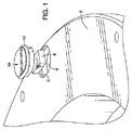
図1は、RFIDチップと、チップ収納栓(chip housing plug)と、チップ及び栓を受け入れるバッキング・プレートの穴と、の複合体を示す、ターゲット/バッキング・プレート組立体の裏側または水側の斜視図である。 FIG. 1 is a perspective view of the back side or water side of a target / backing plate assembly showing a composite of an RFID chip, a chip housing plug, and a hole in the backing plate that receives the chip and plug. FIG.
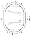
図2は、バッキング・プレートの穴の底部に沿って配置するのに適した栓の開放端部側から見たチップ収納栓の底面図である。 FIG. 2 is a bottom view of the chip receiving plug as viewed from the open end side of the plug suitable for placement along the bottom of the hole in the backing plate.
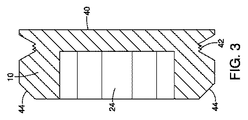
図3は、図2の直線及び矢印3−3に沿った栓の断面図である。 FIG. 3 is a cross-sectional view of the plug along the straight line and the arrow 3-3 in FIG.
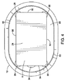
図4は、栓の凹状エリアにチップが密着状態で封入された状態で示されていることを除いて、図2に示されているものと類似した平面図である。 FIG. 4 is a plan view similar to that shown in FIG. 2 except that the tip is shown in close contact with the recessed area of the plug.
図1には、バッキング・プレート2の水側または裏側が示されている。当該バッキング・プレート2の裏側に対して反対の側に沿ってスパッタ・ターゲット(不図示)が載置され、当該ターゲットのフランジが当該バッキング・プレート2の外周囲を被覆していることに注目すべきである。図1に示された当該バッキング・プレート2の側面は、冷却水回路や類似の設計がここで当該バッキング・プレートに衝突して当該被覆状態のターゲットから動作中に熱を除去するので、一般的に水側と呼ばれる。 In FIG. 1, the water side or back side of the backing plate 2 is shown. Note that a sputter target (not shown) is placed along the side opposite to the back side of the backing plate 2 and the flange of the target covers the outer periphery of the backing plate 2. Should. The side of the backing plate 2 shown in FIG. 1 is common because a cooling water circuit or similar design now strikes the backing plate and removes heat from the coated target during operation. Called the water side.
図1をさらに検討すると、バッキング・プレートのこの水側には穴4が設けられている。当該穴は、当該穴の周囲に形成されている溝部6を含む。RFIDチップはこの図では8として示されており、見て分かるように、チップ収納具(つまり栓)10と穴4の底面との間に配置されている。Oリング12が栓の周囲に設けられ、当該バッキング・プレートに形成された溝部6への収容に適している。
Considering FIG. 1 further, a hole 4 is provided on this water side of the backing plate. The hole includes a groove 6 formed around the hole. The RFID chip is shown as 8 in this figure and, as can be seen, is disposed between the chip holder (ie plug) 10 and the bottom of the hole 4. An O-
図2は、栓10のさらなる特徴を図示している。当該栓は、凹状部分24を取り囲む中実部20を含む。当該凹状部分は、チップの密着収容に適している。図のように、当該凹状部分は概ね、辺が交わる各々の部分に丸すみ部26、28、30、32が設けられた平行四辺形として形成されている。付加的に、辺の一つには設置用空洞34が設けられている。この空洞34は、凹状部分24に対するチップの載置及び除去を助けるように小型工具その他の挿入に適している。
FIG. 2 illustrates further features of the
図3に図示された実施形態では、栓の外面40が示されている。栓が穴4に完全に収容された時に、この外面40により、バッキング・プレート2の裏側に滑らかな平面状表面が得られる。外面40の近くにある栓の上側部分には、溝部42が設けられている。この溝部42は、図1に示されたOリング12を収容し、スパッタリング工程の動作中または中断中にバッキング・プレート2と衝突する冷却水その他からRFIDチップを密封する水密シールとなるように、図1に示された穴の溝部6と係合する。バッキング・プレートの穴4への栓10の摩擦嵌めまたはスナップ嵌めを容易にするように、栓10の底側には傾斜エッジ44が形成されている。こうして当該穴での当該栓の摩擦嵌めまたはスナップ嵌めのため、当該穴内での当該栓の確実な装着を行うのに、溶接や他の広範囲接合技術は必要とされない。
In the embodiment illustrated in FIG. 3, the
図4において、RFIDチップは凹状部分24の中へ密着されて示されている。当該栓の中実部20は凹状部分24を取り囲み、中実部と凹状部分との間の境界は、線形表面50、52、54、56と上述した丸すみ部26、28、30、32とにより画定されている。本発明のこの実施形態において、チップ8の側方部分の各々が、図面では60として示された栓の断面周囲境界からほぼ等距離であることに注意してほしい。
In FIG. 4, the RFID chip is shown in close contact with the recessed
こうして、本発明では、スパッタリング工程で見られる要素、とりわけ液体、からのRFIDタグの隔離とともに最大の読取り/書込み範囲を可能にするのに最適な位置が、スパッタリング・ターゲットのフランジ部分と下方にあるバッキング・プレートの周囲とで維持されることが、上記から明白である。スナップ嵌めは、人が栓及び関連のチップを両手のみで確実に押圧して所定箇所にスナップ結合できるように設計されている。これは、好ましくは「Derlin」ポリアセタール・ホモポリマーから作られて、収納部にチップを密封するOリングと嵌合する。こうしてチップは、精密に予定通りの寸法で水平方向と垂直方向の両方において最適な形で載置された状態となる。 Thus, in the present invention, the optimum position to allow maximum read / write range along with isolation of the RFID tag from elements found in the sputtering process, particularly liquids, is below the flange portion of the sputtering target. It is clear from the above that it is maintained around the backing plate. The snap-fit is designed so that a person can securely press the plug and associated tip with both hands and snap into place. It is preferably made from “Derlin” polyacetal homopolymer and mates with an O-ring that seals the tip into the receptacle. In this way, the chip is placed in an optimal form in both horizontal and vertical directions with precise dimensions as planned.
上記のように、以前提案された設計では、チップをフランジに封入するのにエポキシが利用されていた。この先行技術設計は、側壁からの最適な距離を保証できず、エポキシの正確な配合も保証していない。エポキシ生成の準備に必要とされる手作業工程のため、エポキシには気泡形成が結果的に生じることが多い。 As noted above, previously proposed designs used epoxy to encapsulate the chip in the flange. This prior art design cannot guarantee the optimum distance from the sidewalls, nor does it guarantee the correct formulation of the epoxy. Due to the manual processes required to prepare the epoxy production, the epoxy often results in bubble formation.
本発明の設計では、市販の識別タグを保持するのに「Darlin」を利用する。比較すると、エポキシは3.6の誘電率を有するのに対して、Darlinは3.1の誘電率を有する。誘電率が高くなるほど、それが反射するRFエネルギーは多くなり、そしてアンテナの性能をより低下させる。 The design of the present invention utilizes “Darlin” to hold a commercially available identification tag. In comparison, epoxy has a dielectric constant of 3.6, while Darlin has a dielectric constant of 3.1. The higher the dielectric constant, the more RF energy it reflects and the more poor the antenna performance.
本発明の設計では、市販の識別タグを保持するのに「Derlin」を利用する。比較すると、エポキシは、現場で利用可能となる前に必要とされる養生時間を有するのに対して、Derlin組立体は養生時間を必要としない。一般的な養生時間は20分から24時間である。養生時間が不要になると、製造中に組立体を汚損するリスクが低くなり、サイクル時間を短縮する。 The design of the present invention utilizes “Derlin” to hold a commercially available identification tag. In comparison, epoxies have a curing time that is required before they are available in the field, whereas the Derlin assembly does not require a curing time. Typical curing time is 20 minutes to 24 hours. When no curing time is required, the risk of fouling the assembly during manufacturing is reduced and cycle time is reduced.
スパッタリング・ターゲットでの使用について我々が知っている他の金属中の収納(in-metal housings)は他にない。この収納は、質問器(interrogator)への最適な信号強度での応答を可能にして、最大の読取り/書込み能力を与えるように設計されている。さらに、市販の従来の加工設計は、要素、とりわけ水、を製造から隔離するという要求を考慮していない。本発明の設計では、Oリングの利用により、RFID室へ水が流入するのを防止しながら、必要とされる正確な距離にチップを保持している。 There are no other in-metal housings we know about for use with sputtering targets. This containment is designed to allow maximum signal strength response to the interrogator, giving maximum read / write capability. Furthermore, the conventional processing designs on the market do not take into account the requirement to isolate the elements, especially water, from manufacturing. In the design of the present invention, the use of an O-ring keeps the chip at the exact distance required while preventing water from flowing into the RFID chamber.
本発明によるRFIDチップを備えるスパッタリング・ターゲット/バッキング・プレート組立体は、結果的にポケットの最適化をもたらす。これは、本来の装置製造者の設計指示に反することなく、最大の読取り/書込み範囲にわたってスパッタリング室との最適な二方向通信を必要とする。本発明は、適切な機能性についての本来の装置製造者による要求の設計空間を犠牲にしないように、金属表面に埋め込まれる必要がある。ポケット表面は外部アンテナの送信路に対して垂直にチップを維持し、またポケットはターゲット外径に一点で接しなければならない。 A sputtering target / backing plate assembly comprising an RFID chip according to the present invention results in pocket optimization. This requires optimal two-way communication with the sputtering chamber over the maximum read / write range without violating the original equipment manufacturer's design instructions. The present invention needs to be embedded in the metal surface so as not to sacrifice the design space required by the original device manufacturer for proper functionality. The pocket surface must keep the tip perpendicular to the transmission path of the external antenna, and the pocket must touch the target outer diameter at a single point.
2 バッキング・プレート
4 穴
6 溝部
8 RFIDチップ
10 栓
12 Oリング
20 中実部
24 凹状部分
26、28、30、32 丸すみ部
34 設置空洞
40 栓の外面
42 溝部
44 傾斜エッジ
50、52、54、56 線形表面
60 断面周囲境界
2 Backing plate 4 Hole 6 Groove portion 8
Claims (14)
当該栓が外面と凹状部分と中実部とを含み、当該栓の当該中実部が当該凹状部分の少なくとも一部分と境界を接し、
当該凹状部分が、当該RFIDタグを中に確実に収容するように構成されている、
スパッタ・ターゲット/バッキング・プレート組立体におけるRFIDタグ格納複合体。 A hole formed in one of the backing plate or the sputter target and a stopper suitable for tight insertion into the hole,
The plug includes an outer surface, a concave portion, and a solid portion, and the solid portion of the plug touches at least a portion of the concave portion;
The concave portion is configured to securely accommodate the RFID tag therein;
RFID tag storage complex in a sputter target / backing plate assembly.
14. The composite according to claim 13, wherein the Al alloy is Al0.5Cu.
Applications Claiming Priority (5)
| Application Number | Priority Date | Filing Date | Title |
|---|---|---|---|
| US201462004939P | 2014-05-30 | 2014-05-30 | |
| US62/004,939 | 2014-05-30 | ||
| US201462092419P | 2014-12-16 | 2014-12-16 | |
| US62/092,419 | 2014-12-16 | ||
| PCT/US2015/030561 WO2015183554A1 (en) | 2014-05-30 | 2015-05-13 | Radio frequency identification in-metal installation and isolation for sputtering target |
Publications (1)
| Publication Number | Publication Date |
|---|---|
| JP2017519902A true JP2017519902A (en) | 2017-07-20 |
Family
ID=54699542
Family Applications (1)
| Application Number | Title | Priority Date | Filing Date |
|---|---|---|---|
| JP2016569883A Pending JP2017519902A (en) | 2014-05-30 | 2015-05-13 | Installation and insulation of radio frequency identification devices (RFIDs) in metals for sputtering targets |
Country Status (6)
| Country | Link |
|---|---|
| US (1) | US20170098529A1 (en) |
| JP (1) | JP2017519902A (en) |
| KR (1) | KR20170012274A (en) |
| CN (1) | CN106462789A (en) |
| TW (1) | TW201544615A (en) |
| WO (1) | WO2015183554A1 (en) |
Cited By (1)
| Publication number | Priority date | Publication date | Assignee | Title |
|---|---|---|---|---|
| JP2023507093A (en) * | 2019-12-19 | 2023-02-21 | ラム リサーチ コーポレーション | Encapsulated RFID in consumable chamber parts |
Families Citing this family (4)
| Publication number | Priority date | Publication date | Assignee | Title |
|---|---|---|---|---|
| WO2015138091A1 (en) * | 2014-03-14 | 2015-09-17 | Applied Materials, Inc. | Smart chamber and smart chamber components |
| US10896812B2 (en) * | 2017-01-25 | 2021-01-19 | Materion Corporation | Sputtering target having RFID information |
| BE1026859B1 (en) * | 2018-10-22 | 2020-07-14 | Soleras Advanced Coatings Bv | Microwave with integrated circuit for monitoring and control |
| KR102165392B1 (en) * | 2019-05-15 | 2020-10-16 | 와이엠씨 주식회사 | Target for sputtering device capable of detecting critical consumption state |
Family Cites Families (13)
| Publication number | Priority date | Publication date | Assignee | Title |
|---|---|---|---|---|
| US5284561A (en) * | 1991-11-13 | 1994-02-08 | Materials Research Corporation | Method and apparatus for sputter coating employing machine readable indicia carried by target assembly |
| JPH09176849A (en) * | 1995-12-22 | 1997-07-08 | Applied Materials Inc | Assembly of sputtering target |
| FR2784364B1 (en) * | 1998-10-13 | 2000-12-15 | Plastic Omnium Cie | BIN FOR THE COLLECTION OF WASTE, EQUIPPED WITH A TRANSPONDER |
| DE10196880T1 (en) * | 2000-11-20 | 2003-12-18 | Seagate Technology Llc | RF ID tag attachment to a disk drive |
| DE60136098D1 (en) * | 2000-12-18 | 2008-11-20 | Tosoh Smd Inc | LOW TEMPERATURE PROCEDURE FOR SPUTTER TARGET / FOUNDATIONS |
| US6708870B2 (en) * | 2002-05-24 | 2004-03-23 | Praxair S.T. Technology, Inc. | Method for forming sputter target assemblies |
| US20050051606A1 (en) * | 2003-09-09 | 2005-03-10 | Rene Perrot | Method of manufacturing an extended life sputter target assembly and product thereof |
| US7861931B2 (en) * | 2006-11-06 | 2011-01-04 | Mastercard International, Inc. | Method, apparatus, assembly and kit for identification token |
| US7901552B2 (en) * | 2007-10-05 | 2011-03-08 | Applied Materials, Inc. | Sputtering target with grooves and intersecting channels |
| US8133368B2 (en) * | 2008-10-31 | 2012-03-13 | Applied Materials, Inc. | Encapsulated sputtering target |
| CN103492608B (en) * | 2011-02-14 | 2016-04-13 | 东曹Smd有限公司 | Diffusion bonded sputtering target assembly and method of manufacture |
| US8776644B2 (en) * | 2012-01-23 | 2014-07-15 | Stanley Black & Decker, Inc. | Electronic identifier attachment for inventory items |
| WO2015138091A1 (en) * | 2014-03-14 | 2015-09-17 | Applied Materials, Inc. | Smart chamber and smart chamber components |
-
2015
- 2015-05-12 TW TW104115002A patent/TW201544615A/en unknown
- 2015-05-13 KR KR1020167033267A patent/KR20170012274A/en not_active Withdrawn
- 2015-05-13 US US15/314,554 patent/US20170098529A1/en not_active Abandoned
- 2015-05-13 WO PCT/US2015/030561 patent/WO2015183554A1/en not_active Ceased
- 2015-05-13 CN CN201580028521.0A patent/CN106462789A/en active Pending
- 2015-05-13 JP JP2016569883A patent/JP2017519902A/en active Pending
Cited By (2)
| Publication number | Priority date | Publication date | Assignee | Title |
|---|---|---|---|---|
| JP2023507093A (en) * | 2019-12-19 | 2023-02-21 | ラム リサーチ コーポレーション | Encapsulated RFID in consumable chamber parts |
| JP7657802B2 (en) | 2019-12-19 | 2025-04-07 | ラム リサーチ コーポレーション | Encapsulated RFID in consumable chamber parts |
Also Published As
| Publication number | Publication date |
|---|---|
| KR20170012274A (en) | 2017-02-02 |
| TW201544615A (en) | 2015-12-01 |
| US20170098529A1 (en) | 2017-04-06 |
| CN106462789A (en) | 2017-02-22 |
| WO2015183554A1 (en) | 2015-12-03 |
Similar Documents
| Publication | Publication Date | Title |
|---|---|---|
| JP2017519902A (en) | Installation and insulation of radio frequency identification devices (RFIDs) in metals for sputtering targets | |
| US10930479B2 (en) | Smart chamber and smart chamber components | |
| JP5651145B2 (en) | Target structure for physical vapor deposition | |
| KR101505017B1 (en) | Electromagnetic shielding sheet for antenna, and munufacturing method thereof, and antenna comprising the same, and battery pack comprising the antenna | |
| US20040035698A1 (en) | Friction fit target assembly for high power sputtering operation | |
| US7561015B2 (en) | Magnet secured in a two part shell | |
| WO2007146502A3 (en) | Bonded chip assembly with a micro-mover for microelectromechanical systems | |
| US9759988B2 (en) | Camera features of an electronic device | |
| JP2011202217A (en) | Magnetron sputtering apparatus and sputtering method | |
| GB2147916A (en) | Cathodic evaporation of ferromagnetic targets | |
| CN115023777A (en) | Method for manufacturing shielding magnet and shielding magnet manufactured based on method | |
| US20060017520A1 (en) | Ferrite circulator having alignment members | |
| JPH06108241A (en) | Sputtering equipment | |
| TWI515322B (en) | A magnetic material sputtering target is provided on the back of the target | |
| US8052852B2 (en) | Magnetron sputtering cathode mechanism | |
| US20070007130A1 (en) | Enhanced magnetron sputtering target | |
| KR20250009256A (en) | Method for Manufacturing shielding magnet | |
| TWI457456B (en) | Control of erosion profile on a dielectric rf sputter target | |
| US20250243578A1 (en) | Mask and Preparation Method Thereof | |
| WO2007066204A2 (en) | Apparatus and method for adapting a conductive object to accept a communication device | |
| US10115574B2 (en) | Hermetically sealed magnetic keeper cathode | |
| JP2016003388A (en) | Plate member fixing mechanism, PVD processing apparatus, and plate member fixing method | |
| JP2015218382A (en) | Parts storage and parts holder | |
| JP2602807B2 (en) | Target assembly for spatter | |
| JP2009167492A (en) | Film deposition source, and sputtering system |