JP2017516141A - 発光ダイオードデジタルマイクロミラーデバイスイルミネータ - Google Patents
発光ダイオードデジタルマイクロミラーデバイスイルミネータ Download PDFInfo
- Publication number
- JP2017516141A JP2017516141A JP2016565687A JP2016565687A JP2017516141A JP 2017516141 A JP2017516141 A JP 2017516141A JP 2016565687 A JP2016565687 A JP 2016565687A JP 2016565687 A JP2016565687 A JP 2016565687A JP 2017516141 A JP2017516141 A JP 2017516141A
- Authority
- JP
- Japan
- Prior art keywords
- led
- aperture
- output
- optical system
- condensing optical
- Prior art date
- Legal status (The legal status is an assumption and is not a legal conclusion. Google has not performed a legal analysis and makes no representation as to the accuracy of the status listed.)
- Pending
Links
- 230000003287 optical effect Effects 0.000 claims abstract description 61
- 238000003384 imaging method Methods 0.000 claims abstract description 50
- 238000005286 illumination Methods 0.000 claims abstract description 45
- 238000004891 communication Methods 0.000 claims abstract description 8
- 239000011521 glass Substances 0.000 claims description 12
- 230000005540 biological transmission Effects 0.000 claims description 6
- 238000009826 distribution Methods 0.000 claims description 5
- 230000000694 effects Effects 0.000 claims description 5
- 150000001875 compounds Chemical class 0.000 claims description 2
- 230000008878 coupling Effects 0.000 claims description 2
- 238000010168 coupling process Methods 0.000 claims description 2
- 238000005859 coupling reaction Methods 0.000 claims description 2
- 239000000463 material Substances 0.000 abstract description 16
- 238000001459 lithography Methods 0.000 abstract description 5
- 238000003848 UV Light-Curing Methods 0.000 abstract description 4
- 230000005284 excitation Effects 0.000 abstract description 2
- 230000005855 radiation Effects 0.000 abstract description 2
- 239000010432 diamond Substances 0.000 description 16
- 229910003460 diamond Inorganic materials 0.000 description 16
- XLYOFNOQVPJJNP-UHFFFAOYSA-N water Substances O XLYOFNOQVPJJNP-UHFFFAOYSA-N 0.000 description 14
- RYGMFSIKBFXOCR-UHFFFAOYSA-N Copper Chemical compound [Cu] RYGMFSIKBFXOCR-UHFFFAOYSA-N 0.000 description 12
- 229910052802 copper Inorganic materials 0.000 description 12
- 239000010949 copper Substances 0.000 description 12
- 230000003595 spectral effect Effects 0.000 description 9
- 238000013461 design Methods 0.000 description 8
- 239000000758 substrate Substances 0.000 description 8
- 230000008901 benefit Effects 0.000 description 6
- 230000007423 decrease Effects 0.000 description 6
- 238000004519 manufacturing process Methods 0.000 description 6
- 229910000679 solder Inorganic materials 0.000 description 6
- 125000006850 spacer group Chemical group 0.000 description 6
- 238000001723 curing Methods 0.000 description 5
- 230000001419 dependent effect Effects 0.000 description 5
- 230000006870 function Effects 0.000 description 5
- 229910052751 metal Inorganic materials 0.000 description 5
- 239000002184 metal Substances 0.000 description 5
- 238000000034 method Methods 0.000 description 5
- 238000003491 array Methods 0.000 description 4
- 230000004907 flux Effects 0.000 description 4
- VYPSYNLAJGMNEJ-UHFFFAOYSA-N Silicium dioxide Chemical compound O=[Si]=O VYPSYNLAJGMNEJ-UHFFFAOYSA-N 0.000 description 3
- BQCADISMDOOEFD-UHFFFAOYSA-N Silver Chemical compound [Ag] BQCADISMDOOEFD-UHFFFAOYSA-N 0.000 description 3
- 238000013459 approach Methods 0.000 description 3
- 230000008859 change Effects 0.000 description 3
- 239000011248 coating agent Substances 0.000 description 3
- 238000000576 coating method Methods 0.000 description 3
- 239000004020 conductor Substances 0.000 description 3
- 238000005516 engineering process Methods 0.000 description 3
- 239000004519 grease Substances 0.000 description 3
- 230000008569 process Effects 0.000 description 3
- 230000009467 reduction Effects 0.000 description 3
- 229910052709 silver Inorganic materials 0.000 description 3
- 239000004332 silver Substances 0.000 description 3
- XUIMIQQOPSSXEZ-UHFFFAOYSA-N Silicon Chemical compound [Si] XUIMIQQOPSSXEZ-UHFFFAOYSA-N 0.000 description 2
- 238000000862 absorption spectrum Methods 0.000 description 2
- 230000004075 alteration Effects 0.000 description 2
- 238000002048 anodisation reaction Methods 0.000 description 2
- 230000003467 diminishing effect Effects 0.000 description 2
- 239000005350 fused silica glass Substances 0.000 description 2
- PCHJSUWPFVWCPO-UHFFFAOYSA-N gold Chemical group [Au] PCHJSUWPFVWCPO-UHFFFAOYSA-N 0.000 description 2
- 229910052737 gold Inorganic materials 0.000 description 2
- 239000010931 gold Substances 0.000 description 2
- 230000006872 improvement Effects 0.000 description 2
- 238000012423 maintenance Methods 0.000 description 2
- 230000002829 reductive effect Effects 0.000 description 2
- 229910052710 silicon Inorganic materials 0.000 description 2
- 239000010703 silicon Substances 0.000 description 2
- 239000007787 solid Substances 0.000 description 2
- 239000006096 absorbing agent Substances 0.000 description 1
- 239000000853 adhesive Substances 0.000 description 1
- 230000001070 adhesive effect Effects 0.000 description 1
- 230000003667 anti-reflective effect Effects 0.000 description 1
- QVGXLLKOCUKJST-UHFFFAOYSA-N atomic oxygen Chemical compound [O] QVGXLLKOCUKJST-UHFFFAOYSA-N 0.000 description 1
- 230000009286 beneficial effect Effects 0.000 description 1
- 230000002146 bilateral effect Effects 0.000 description 1
- 230000015556 catabolic process Effects 0.000 description 1
- 230000001010 compromised effect Effects 0.000 description 1
- 238000001816 cooling Methods 0.000 description 1
- 238000012937 correction Methods 0.000 description 1
- 230000001186 cumulative effect Effects 0.000 description 1
- 230000003247 decreasing effect Effects 0.000 description 1
- 238000006731 degradation reaction Methods 0.000 description 1
- 230000000593 degrading effect Effects 0.000 description 1
- 238000009792 diffusion process Methods 0.000 description 1
- 239000006185 dispersion Substances 0.000 description 1
- 238000001704 evaporation Methods 0.000 description 1
- 230000008020 evaporation Effects 0.000 description 1
- 239000012530 fluid Substances 0.000 description 1
- 238000010438 heat treatment Methods 0.000 description 1
- 230000005764 inhibitory process Effects 0.000 description 1
- 239000000976 ink Substances 0.000 description 1
- 238000009434 installation Methods 0.000 description 1
- 230000003993 interaction Effects 0.000 description 1
- 238000005304 joining Methods 0.000 description 1
- 230000000670 limiting effect Effects 0.000 description 1
- 230000007774 longterm Effects 0.000 description 1
- QSHDDOUJBYECFT-UHFFFAOYSA-N mercury Chemical compound [Hg] QSHDDOUJBYECFT-UHFFFAOYSA-N 0.000 description 1
- 229910052753 mercury Inorganic materials 0.000 description 1
- 238000012544 monitoring process Methods 0.000 description 1
- 238000000465 moulding Methods 0.000 description 1
- TWNQGVIAIRXVLR-UHFFFAOYSA-N oxo(oxoalumanyloxy)alumane Chemical compound O=[Al]O[Al]=O TWNQGVIAIRXVLR-UHFFFAOYSA-N 0.000 description 1
- 229910052760 oxygen Inorganic materials 0.000 description 1
- 239000001301 oxygen Substances 0.000 description 1
- 238000004806 packaging method and process Methods 0.000 description 1
- 238000000016 photochemical curing Methods 0.000 description 1
- 229920001296 polysiloxane Polymers 0.000 description 1
- 238000004321 preservation Methods 0.000 description 1
- 238000007639 printing Methods 0.000 description 1
- 239000010453 quartz Substances 0.000 description 1
- 230000000717 retained effect Effects 0.000 description 1
- 230000002441 reversible effect Effects 0.000 description 1
- 150000003839 salts Chemical class 0.000 description 1
- 229910052594 sapphire Inorganic materials 0.000 description 1
- 239000010980 sapphire Substances 0.000 description 1
- 238000004088 simulation Methods 0.000 description 1
- 238000001228 spectrum Methods 0.000 description 1
- 239000004575 stone Substances 0.000 description 1
- 239000000126 substance Substances 0.000 description 1
- 230000007704 transition Effects 0.000 description 1
- 239000011800 void material Substances 0.000 description 1
- 229910052724 xenon Inorganic materials 0.000 description 1
- FHNFHKCVQCLJFQ-UHFFFAOYSA-N xenon atom Chemical compound [Xe] FHNFHKCVQCLJFQ-UHFFFAOYSA-N 0.000 description 1
Images

Classifications
-
- G—PHYSICS
- G02—OPTICS
- G02B—OPTICAL ELEMENTS, SYSTEMS OR APPARATUS
- G02B19/00—Condensers, e.g. light collectors or similar non-imaging optics
- G02B19/0004—Condensers, e.g. light collectors or similar non-imaging optics characterised by the optical means employed
- G02B19/0009—Condensers, e.g. light collectors or similar non-imaging optics characterised by the optical means employed having refractive surfaces only
- G02B19/0014—Condensers, e.g. light collectors or similar non-imaging optics characterised by the optical means employed having refractive surfaces only at least one surface having optical power
-
- G—PHYSICS
- G02—OPTICS
- G02B—OPTICAL ELEMENTS, SYSTEMS OR APPARATUS
- G02B19/00—Condensers, e.g. light collectors or similar non-imaging optics
- G02B19/0033—Condensers, e.g. light collectors or similar non-imaging optics characterised by the use
- G02B19/0047—Condensers, e.g. light collectors or similar non-imaging optics characterised by the use for use with a light source
- G02B19/0061—Condensers, e.g. light collectors or similar non-imaging optics characterised by the use for use with a light source the light source comprising a LED
-
- G—PHYSICS
- G02—OPTICS
- G02B—OPTICAL ELEMENTS, SYSTEMS OR APPARATUS
- G02B19/00—Condensers, e.g. light collectors or similar non-imaging optics
- G02B19/0004—Condensers, e.g. light collectors or similar non-imaging optics characterised by the optical means employed
- G02B19/0028—Condensers, e.g. light collectors or similar non-imaging optics characterised by the optical means employed refractive and reflective surfaces, e.g. non-imaging catadioptric systems
-
- G—PHYSICS
- G02—OPTICS
- G02B—OPTICAL ELEMENTS, SYSTEMS OR APPARATUS
- G02B19/00—Condensers, e.g. light collectors or similar non-imaging optics
- G02B19/0033—Condensers, e.g. light collectors or similar non-imaging optics characterised by the use
- G02B19/0047—Condensers, e.g. light collectors or similar non-imaging optics characterised by the use for use with a light source
- G02B19/0061—Condensers, e.g. light collectors or similar non-imaging optics characterised by the use for use with a light source the light source comprising a LED
- G02B19/0066—Condensers, e.g. light collectors or similar non-imaging optics characterised by the use for use with a light source the light source comprising a LED in the form of an LED array
-
- G—PHYSICS
- G02—OPTICS
- G02B—OPTICAL ELEMENTS, SYSTEMS OR APPARATUS
- G02B27/00—Optical systems or apparatus not provided for by any of the groups G02B1/00 - G02B26/00, G02B30/00
- G02B27/09—Beam shaping, e.g. changing the cross-sectional area, not otherwise provided for
- G02B27/0938—Using specific optical elements
- G02B27/0994—Fibers, light pipes
-
- G—PHYSICS
- G03—PHOTOGRAPHY; CINEMATOGRAPHY; ANALOGOUS TECHNIQUES USING WAVES OTHER THAN OPTICAL WAVES; ELECTROGRAPHY; HOLOGRAPHY
- G03B—APPARATUS OR ARRANGEMENTS FOR TAKING PHOTOGRAPHS OR FOR PROJECTING OR VIEWING THEM; APPARATUS OR ARRANGEMENTS EMPLOYING ANALOGOUS TECHNIQUES USING WAVES OTHER THAN OPTICAL WAVES; ACCESSORIES THEREFOR
- G03B21/00—Projectors or projection-type viewers; Accessories therefor
- G03B21/14—Details
- G03B21/20—Lamp housings
- G03B21/208—Homogenising, shaping of the illumination light
-
- G—PHYSICS
- G03—PHOTOGRAPHY; CINEMATOGRAPHY; ANALOGOUS TECHNIQUES USING WAVES OTHER THAN OPTICAL WAVES; ELECTROGRAPHY; HOLOGRAPHY
- G03F—PHOTOMECHANICAL PRODUCTION OF TEXTURED OR PATTERNED SURFACES, e.g. FOR PRINTING, FOR PROCESSING OF SEMICONDUCTOR DEVICES; MATERIALS THEREFOR; ORIGINALS THEREFOR; APPARATUS SPECIALLY ADAPTED THEREFOR
- G03F7/00—Photomechanical, e.g. photolithographic, production of textured or patterned surfaces, e.g. printing surfaces; Materials therefor, e.g. comprising photoresists; Apparatus specially adapted therefor
- G03F7/70—Microphotolithographic exposure; Apparatus therefor
- G03F7/70008—Production of exposure light, i.e. light sources
- G03F7/7005—Production of exposure light, i.e. light sources by multiple sources, e.g. light-emitting diodes [LED] or light source arrays
-
- G—PHYSICS
- G03—PHOTOGRAPHY; CINEMATOGRAPHY; ANALOGOUS TECHNIQUES USING WAVES OTHER THAN OPTICAL WAVES; ELECTROGRAPHY; HOLOGRAPHY
- G03F—PHOTOMECHANICAL PRODUCTION OF TEXTURED OR PATTERNED SURFACES, e.g. FOR PRINTING, FOR PROCESSING OF SEMICONDUCTOR DEVICES; MATERIALS THEREFOR; ORIGINALS THEREFOR; APPARATUS SPECIALLY ADAPTED THEREFOR
- G03F7/00—Photomechanical, e.g. photolithographic, production of textured or patterned surfaces, e.g. printing surfaces; Materials therefor, e.g. comprising photoresists; Apparatus specially adapted therefor
- G03F7/70—Microphotolithographic exposure; Apparatus therefor
- G03F7/70058—Mask illumination systems
- G03F7/7015—Details of optical elements
- G03F7/70166—Capillary or channel elements, e.g. nested extreme ultraviolet [EUV] mirrors or shells, optical fibers or light guides
-
- G—PHYSICS
- G03—PHOTOGRAPHY; CINEMATOGRAPHY; ANALOGOUS TECHNIQUES USING WAVES OTHER THAN OPTICAL WAVES; ELECTROGRAPHY; HOLOGRAPHY
- G03F—PHOTOMECHANICAL PRODUCTION OF TEXTURED OR PATTERNED SURFACES, e.g. FOR PRINTING, FOR PROCESSING OF SEMICONDUCTOR DEVICES; MATERIALS THEREFOR; ORIGINALS THEREFOR; APPARATUS SPECIALLY ADAPTED THEREFOR
- G03F7/00—Photomechanical, e.g. photolithographic, production of textured or patterned surfaces, e.g. printing surfaces; Materials therefor, e.g. comprising photoresists; Apparatus specially adapted therefor
- G03F7/70—Microphotolithographic exposure; Apparatus therefor
- G03F7/70058—Mask illumination systems
- G03F7/702—Reflective illumination, i.e. reflective optical elements other than folding mirrors, e.g. extreme ultraviolet [EUV] illumination systems
-
- G—PHYSICS
- G03—PHOTOGRAPHY; CINEMATOGRAPHY; ANALOGOUS TECHNIQUES USING WAVES OTHER THAN OPTICAL WAVES; ELECTROGRAPHY; HOLOGRAPHY
- G03F—PHOTOMECHANICAL PRODUCTION OF TEXTURED OR PATTERNED SURFACES, e.g. FOR PRINTING, FOR PROCESSING OF SEMICONDUCTOR DEVICES; MATERIALS THEREFOR; ORIGINALS THEREFOR; APPARATUS SPECIALLY ADAPTED THEREFOR
- G03F7/00—Photomechanical, e.g. photolithographic, production of textured or patterned surfaces, e.g. printing surfaces; Materials therefor, e.g. comprising photoresists; Apparatus specially adapted therefor
- G03F7/70—Microphotolithographic exposure; Apparatus therefor
- G03F7/70216—Mask projection systems
- G03F7/70283—Mask effects on the imaging process
- G03F7/70291—Addressable masks, e.g. spatial light modulators [SLMs], digital micro-mirror devices [DMDs] or liquid crystal display [LCD] patterning devices
-
- G—PHYSICS
- G03—PHOTOGRAPHY; CINEMATOGRAPHY; ANALOGOUS TECHNIQUES USING WAVES OTHER THAN OPTICAL WAVES; ELECTROGRAPHY; HOLOGRAPHY
- G03F—PHOTOMECHANICAL PRODUCTION OF TEXTURED OR PATTERNED SURFACES, e.g. FOR PRINTING, FOR PROCESSING OF SEMICONDUCTOR DEVICES; MATERIALS THEREFOR; ORIGINALS THEREFOR; APPARATUS SPECIALLY ADAPTED THEREFOR
- G03F7/00—Photomechanical, e.g. photolithographic, production of textured or patterned surfaces, e.g. printing surfaces; Materials therefor, e.g. comprising photoresists; Apparatus specially adapted therefor
- G03F7/70—Microphotolithographic exposure; Apparatus therefor
- G03F7/70383—Direct write, i.e. pattern is written directly without the use of a mask by one or multiple beams
- G03F7/70391—Addressable array sources specially adapted to produce patterns, e.g. addressable LED arrays
-
- H—ELECTRICITY
- H04—ELECTRIC COMMUNICATION TECHNIQUE
- H04N—PICTORIAL COMMUNICATION, e.g. TELEVISION
- H04N9/00—Details of colour television systems
- H04N9/12—Picture reproducers
- H04N9/31—Projection devices for colour picture display, e.g. using electronic spatial light modulators [ESLM]
- H04N9/3141—Constructional details thereof
- H04N9/315—Modulator illumination systems
-
- G—PHYSICS
- G02—OPTICS
- G02B—OPTICAL ELEMENTS, SYSTEMS OR APPARATUS
- G02B13/00—Optical objectives specially designed for the purposes specified below
- G02B13/22—Telecentric objectives or lens systems
-
- G—PHYSICS
- G02—OPTICS
- G02B—OPTICAL ELEMENTS, SYSTEMS OR APPARATUS
- G02B19/00—Condensers, e.g. light collectors or similar non-imaging optics
- G02B19/0033—Condensers, e.g. light collectors or similar non-imaging optics characterised by the use
- G02B19/0095—Condensers, e.g. light collectors or similar non-imaging optics characterised by the use for use with ultraviolet radiation
-
- G—PHYSICS
- G02—OPTICS
- G02B—OPTICAL ELEMENTS, SYSTEMS OR APPARATUS
- G02B26/00—Optical devices or arrangements for the control of light using movable or deformable optical elements
- G02B26/08—Optical devices or arrangements for the control of light using movable or deformable optical elements for controlling the direction of light
- G02B26/0816—Optical devices or arrangements for the control of light using movable or deformable optical elements for controlling the direction of light by means of one or more reflecting elements
- G02B26/0833—Optical devices or arrangements for the control of light using movable or deformable optical elements for controlling the direction of light by means of one or more reflecting elements the reflecting element being a micromechanical device, e.g. a MEMS mirror, DMD
-
- G—PHYSICS
- G03—PHOTOGRAPHY; CINEMATOGRAPHY; ANALOGOUS TECHNIQUES USING WAVES OTHER THAN OPTICAL WAVES; ELECTROGRAPHY; HOLOGRAPHY
- G03B—APPARATUS OR ARRANGEMENTS FOR TAKING PHOTOGRAPHS OR FOR PROJECTING OR VIEWING THEM; APPARATUS OR ARRANGEMENTS EMPLOYING ANALOGOUS TECHNIQUES USING WAVES OTHER THAN OPTICAL WAVES; ACCESSORIES THEREFOR
- G03B21/00—Projectors or projection-type viewers; Accessories therefor
- G03B21/005—Projectors using an electronic spatial light modulator but not peculiar thereto
- G03B21/008—Projectors using an electronic spatial light modulator but not peculiar thereto using micromirror devices
-
- G—PHYSICS
- G03—PHOTOGRAPHY; CINEMATOGRAPHY; ANALOGOUS TECHNIQUES USING WAVES OTHER THAN OPTICAL WAVES; ELECTROGRAPHY; HOLOGRAPHY
- G03B—APPARATUS OR ARRANGEMENTS FOR TAKING PHOTOGRAPHS OR FOR PROJECTING OR VIEWING THEM; APPARATUS OR ARRANGEMENTS EMPLOYING ANALOGOUS TECHNIQUES USING WAVES OTHER THAN OPTICAL WAVES; ACCESSORIES THEREFOR
- G03B21/00—Projectors or projection-type viewers; Accessories therefor
- G03B21/14—Details
- G03B21/20—Lamp housings
- G03B21/2006—Lamp housings characterised by the light source
- G03B21/2033—LED or laser light sources
Landscapes
- Physics & Mathematics (AREA)
- General Physics & Mathematics (AREA)
- Optics & Photonics (AREA)
- Engineering & Computer Science (AREA)
- Multimedia (AREA)
- Signal Processing (AREA)
- Projection Apparatus (AREA)
- General Engineering & Computer Science (AREA)
- High Energy & Nuclear Physics (AREA)
- Optical Elements Other Than Lenses (AREA)
- Exposure And Positioning Against Photoresist Photosensitive Materials (AREA)
- Spectroscopy & Molecular Physics (AREA)
Abstract
Description
Claims (27)
- マイクロミラーデバイスのための発光ダイオード(LED)プロジェクタであって、
少なくとも1つのLEDダイと、
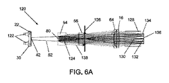
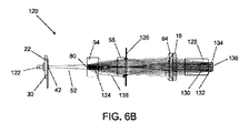
前記少なくとも1つのLEDダイと光通信する入力アパーチャと、出力アパーチャと、を有する非結像集光光学系と、
前記非結像集光光学系の前記出力アパーチャと光通信し、かつ、像面における前記出力アパーチャの像を生成するように構成されたレンズ系であって、前記非結像集光光学系の前記出力アパーチャを含む物体空間でテレセントリックである、レンズ系と、を備える発光ダイオード(LED)プロジェクタ。 - 前記レンズ系は、前記像面を含む像空間においてテレセントリックである、請求項1に記載のLEDプロジェクタ。
- 前記入力アパーチャ及び前記出力アパーチャが矩形アパーチャである、請求項1に記載のLEDプロジェクタ。
- 前記出力アパーチャは、前記非結像集光光学系の出力面の寸法によって規定される、請求項1に記載のLEDプロジェクタ。
- 前記出力アパーチャは、前記非結像集光光学系の出力面上に蒸着された反射ミラーの内側の矩形透過領域によって規定される、請求項3に記載のLEDプロジェクタ。
- 前記出力アパーチャは、前記非結像集光光学系の前記出力面に隣接して配置されたウインドウ上に蒸着された反射ミラーの内側の矩形透過領域によって規定される、請求項3に記載のLEDプロジェクタ。
- 前記出力アパーチャは、前記非結像集光光学系の前記出力面と直接光通信するレンズ素子の前面上に蒸着された反射ミラーの内側の矩形透過領域によって規定される、請求項3に記載のLEDプロジェクタ。
- 前記矩形アパーチャは、デジタルマイクロミラーデバイスのアスペクト比に実質的に一致するアスペクト比を有する、請求項3に記載のLEDプロジェクタ。
- 前記非結像集光光学系はテーパ形状のガラスライトパイプである、請求項1の記載のLEDプロジェクタ。
- 前記非結像集光光学系は複合パラボラ集光器である、請求項1に記載のLEDプロジェクタ。
- 前記非結像集光光学系は、前記レンズ系のアパーチャストップを余分に満たす非近接場分布を提供するように構成される、請求項1に記載のLEDプロジェクタ。
- 前記非結像集光光学系は、前記レンズ系のアパーチャストップに実質的に一致させられる非近接場分布を提供するように構成される、請求項1に記載のLEDプロジェクタ。
- 前記少なくとも1つのLEDダイは紫外発光LEDのアレイを備える、請求項1に記載のLEDプロジェクタ。
- デジタルマイクロミラー照明システムであって、
少なくとも1つの発光ダイオード(LED)ダイと、
前記少なくとも1つのLEDダイと光通信する入力アパーチャと、出力アパーチャと、を有する非結像集光光学系と、
前記非結像集光光学系の前記出力アパーチャと光通信し、かつ、像面における前記出力アパーチャの像を生成するように構成されたレンズ系であって、前記非結像集光光学系の前記出力アパーチャを含む物体空間でテレセントリックである、レンズ系と、
前記像面に配置されたマイクロミラーの平面を含むデジタルマイクロミラーデバイス(DMD)と、を備えるデジタルマイクロミラー照明システム。 - 前記レンズ系は、前記出力アパーチャの像を含む像空間においてテレセントリックである、請求項14に記載のデジタルマイクロミラー照明システム。
- 前記レンズ系と前記DMDとの間に配置された全内部反射カップリングプリズムをさらに備える、請求項14に記載のデジタルマイクロミラー照明システム。
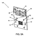
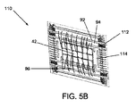
- 前記出力アパーチャで前記非結像集光光学系に当接するテーパ延長部であって、キーストーン効果に起因した非均一性を補償する及び実質的に補正するように決定された角度で傾斜した中空矩形断面を規定する複数の内部反射壁を有するテーパ延長部をさらに備える、請求項14に記載のデジタルマイクロミラー照明システム。
- 前記入力アパーチャ及び前記出力アパーチャは矩形アパーチャである、請求項14に記載のデジタルマイクロミラー照明システム。
- 前記出力アパーチャは、前記非結像集光光学系の出力面の寸法によって規定される、請求項14に記載のデジタルマイクロミラー照明システム。
- 前記出力アパーチャは、前記非結像集光光学系の出力面上に蒸着された反射ミラーの内側の矩形透過領域によって規定される、請求項18に記載のデジタルマイクロミラー照明システム。
- 前記矩形アパーチャは、前記DMDのアスペクト比に実質的に一致するアスペクト比を有する、請求項18に記載のデジタルマイクロミラー照明システム。
- 前記少なくとも1つのLEDダイは紫外発光LEDのアレイを備える、請求項14に記載のデジタルマイクロミラー照明システム。
- マイクロミラーデバイスのための発光ダイオード(LED)プロジェクタであって、
少なくとも1つのLEDダイと、
前記少なくとも1つのLEDダイと光通信する入力アパーチャと、出力アパーチャと、を有する非結像集光光学系と、
前記非結像集光光学系の前記出力アパーチャと光通信し、かつ、像面における前記出力アパーチャの像を生成するように構成されたレンズ系であって、前記非結像集光光学系の前記出力アパーチャを含む物体空間でテレセントリックであり、かつ、前記像平面を含む画像空間でテレセントリックである、レンズ系と、を備える発光ダイオード(LED)プロジェクタ。 - 前記入力アパーチャ及び前記出力アパーチャは矩形アパーチャである、請求項23に記載のLEDプロジェクタ。
- 前記出力アパーチャは、前記非結像集光光学系の出力面上に蒸着された反射ミラーの内側の矩形透過領域によって規定される、請求項24に記載のLEDプロジェクタ。
- 前記出力アパーチャは、前記非結像集光光学系の前記出力面に隣接して配置されたウインドウ上に蒸着された反射ミラーの内側の矩形透過領域によって規定される、請求項24に記載のLEDプロジェクタ。
- 前記出力アパーチャは、前記非結像集光光学系の前記出力面と直接光通信するレンズ素子の前面上に蒸着された反射ミラーの内側の矩形透過領域によって規定される、請求項24に記載のLEDプロジェクタ。
Applications Claiming Priority (3)
| Application Number | Priority Date | Filing Date | Title |
|---|---|---|---|
| US201461991488P | 2014-05-10 | 2014-05-10 | |
| US61/991,488 | 2014-05-10 | ||
| PCT/US2015/029392 WO2015175274A1 (en) | 2014-05-10 | 2015-05-06 | Light emitting diode digital micromirror device illuminator |
Publications (2)
| Publication Number | Publication Date |
|---|---|
| JP2017516141A true JP2017516141A (ja) | 2017-06-15 |
| JP2017516141A5 JP2017516141A5 (ja) | 2018-12-13 |
Family
ID=54368430
Family Applications (1)
| Application Number | Title | Priority Date | Filing Date |
|---|---|---|---|
| JP2016565687A Pending JP2017516141A (ja) | 2014-05-10 | 2015-05-06 | 発光ダイオードデジタルマイクロミラーデバイスイルミネータ |
Country Status (6)
| Country | Link |
|---|---|
| US (2) | US20150325323A1 (ja) |
| EP (2) | EP3143449A4 (ja) |
| JP (1) | JP2017516141A (ja) |
| CA (1) | CA2945982A1 (ja) |
| IL (1) | IL248343A0 (ja) |
| WO (1) | WO2015175274A1 (ja) |
Cited By (1)
| Publication number | Priority date | Publication date | Assignee | Title |
|---|---|---|---|---|
| JP2020506413A (ja) * | 2017-01-19 | 2020-02-27 | イノヴェイションズ イン オプティクス,インコーポレイテッドInnovations In Optics,Inc. | 発光ダイオードデジタルマイクロミラーデバイスイルミネータ |
Families Citing this family (12)
| Publication number | Priority date | Publication date | Assignee | Title |
|---|---|---|---|---|
| US9971135B2 (en) | 2014-05-10 | 2018-05-15 | Innovations In Optics, Inc. | Light emitting diode digital micromirror device illuminator |
| US10180248B2 (en) | 2015-09-02 | 2019-01-15 | ProPhotonix Limited | LED lamp with sensing capabilities |
| JP6655753B2 (ja) * | 2016-07-13 | 2020-02-26 | アプライド マテリアルズ インコーポレイテッドApplied Materials,Incorporated | 照明源としてのマイクロledアレイ |
| US10908507B2 (en) | 2016-07-13 | 2021-02-02 | Applied Materials, Inc. | Micro LED array illumination source |
| WO2019109071A1 (en) * | 2017-12-01 | 2019-06-06 | Chroma Technology Corp. | System and method for preparing laser light for microscopy |
| US11303355B2 (en) | 2018-05-30 | 2022-04-12 | Apple Inc. | Optical structures in directional free-space optical communication systems for portable electronic devices |
| US10700780B2 (en) | 2018-05-30 | 2020-06-30 | Apple Inc. | Systems and methods for adjusting movable lenses in directional free-space optical communication systems for portable electronic devices |
| TWI659239B (zh) * | 2018-11-14 | 2019-05-11 | 大立光電股份有限公司 | 成像光學透鏡組、取像裝置及電子裝置 |
| US11549799B2 (en) | 2019-07-01 | 2023-01-10 | Apple Inc. | Self-mixing interference device for sensing applications |
| CN112666135B (zh) * | 2020-11-26 | 2023-04-21 | 中国科学技术大学 | 一种三维显微成像装置及方法 |
| US12413043B2 (en) | 2021-09-21 | 2025-09-09 | Apple Inc. | Self-mixing interference device with tunable microelectromechanical system |
| WO2026024516A1 (en) * | 2024-07-22 | 2026-01-29 | Innovations In Optics, Inc. | Multispectral illuminator |
Family Cites Families (14)
| Publication number | Priority date | Publication date | Assignee | Title |
|---|---|---|---|---|
| US5442414A (en) * | 1994-05-10 | 1995-08-15 | U. S. Philips Corporation | High contrast illumination system for video projector |
| MXPA05011434A (es) * | 2003-04-24 | 2006-05-31 | Chromnomotion Imaging Applic I | Sistema optico de motor de iluminacion en estado solido. |
| US7029130B2 (en) * | 2003-12-30 | 2006-04-18 | 3M Innovative Properties Company | Contrast and brightness enhancing apertures for illumination displays |
| US20060139580A1 (en) * | 2004-12-29 | 2006-06-29 | Conner Arlie R | Illumination system using multiple light sources with integrating tunnel and projection systems using same |
| US7832878B2 (en) * | 2006-03-06 | 2010-11-16 | Innovations In Optics, Inc. | Light emitting diode projection system |
| US7889430B2 (en) * | 2006-05-09 | 2011-02-15 | Ostendo Technologies, Inc. | LED-based high efficiency illumination systems for use in projection systems |
| JP5642385B2 (ja) * | 2006-06-13 | 2014-12-17 | ウェイヴィーン・インコーポレイテッド | 光源の輝度を増大させるために光をリサイクルする照明システムと方法 |
| EP1955107B1 (en) * | 2006-07-18 | 2012-02-22 | RealD Inc. | Light collectors for projection systems |
| EP2193657A2 (en) * | 2007-09-25 | 2010-06-09 | Explay Ltd. | Micro-projector |
| US20090190101A1 (en) * | 2008-01-28 | 2009-07-30 | International Business Machines Corporation | Double-Reverse Total-Internal-Reflection-Prism Optical Engine |
| WO2010084666A1 (ja) * | 2009-01-20 | 2010-07-29 | コニカミノルタオプト株式会社 | 投影装置 |
| JP5436097B2 (ja) * | 2009-08-25 | 2014-03-05 | 三菱電機株式会社 | 集光光学系及び投写型画像表示装置 |
| US8602567B2 (en) * | 2009-09-29 | 2013-12-10 | Wavien, Inc. | Multiplexing light pipe having enhanced brightness |
| US8403527B2 (en) * | 2010-10-26 | 2013-03-26 | Thomas J. Brukilacchio | Light emitting diode projector |
-
2015
- 2015-05-06 EP EP15792480.4A patent/EP3143449A4/en not_active Withdrawn
- 2015-05-06 JP JP2016565687A patent/JP2017516141A/ja active Pending
- 2015-05-06 US US14/705,202 patent/US20150325323A1/en not_active Abandoned
- 2015-05-06 CA CA2945982A patent/CA2945982A1/en not_active Abandoned
- 2015-05-06 EP EP18178483.6A patent/EP3435132A3/en not_active Withdrawn
- 2015-05-06 WO PCT/US2015/029392 patent/WO2015175274A1/en not_active Ceased
-
2016
- 2016-10-13 IL IL248343A patent/IL248343A0/en unknown
-
2018
- 2018-07-16 US US16/036,167 patent/US20180341094A1/en not_active Abandoned
Cited By (1)
| Publication number | Priority date | Publication date | Assignee | Title |
|---|---|---|---|---|
| JP2020506413A (ja) * | 2017-01-19 | 2020-02-27 | イノヴェイションズ イン オプティクス,インコーポレイテッドInnovations In Optics,Inc. | 発光ダイオードデジタルマイクロミラーデバイスイルミネータ |
Also Published As
| Publication number | Publication date |
|---|---|
| US20180341094A1 (en) | 2018-11-29 |
| EP3143449A1 (en) | 2017-03-22 |
| IL248343A0 (en) | 2016-11-30 |
| WO2015175274A1 (en) | 2015-11-19 |
| EP3435132A2 (en) | 2019-01-30 |
| CA2945982A1 (en) | 2015-11-19 |
| EP3143449A4 (en) | 2018-01-03 |
| US20150325323A1 (en) | 2015-11-12 |
| EP3435132A3 (en) | 2019-04-17 |
Similar Documents
| Publication | Publication Date | Title |
|---|---|---|
| JP2017516141A (ja) | 発光ダイオードデジタルマイクロミラーデバイスイルミネータ | |
| US10409045B2 (en) | Hollow light integrator for light emitting diode digital micromirror device illuminator | |
| JP5850542B2 (ja) | 発光ダイオードプロジェクタ | |
| EP2389536B1 (en) | Light emitting diode linear light for machine vision | |
| US20060175625A1 (en) | Light emitting element, lighting device and surface emission illuminating device using it | |
| US20120217519A1 (en) | Method and structure for encapsulating solid-state light emitting chip and light sources using the encapsulation structure | |
| CN102063000A (zh) | 投影仪设备、叠层型发光二极管器件以及反射型发光二极管单元 | |
| CN104736921A (zh) | 紫外线发光模块以及紫外线照射装置 | |
| CN100541320C (zh) | Led组件以及采用led组件的照明系统和投影系统 | |
| WO2014115194A1 (ja) | 光源、光源ユニットおよびそれを用いた光源モジュール | |
| KR20150143656A (ko) | 발광 장치 및 프로젝션 시스템 | |
| CN108139040A (zh) | 荧光光源装置 | |
| WO2006102846A1 (en) | High efficient light coupling of solid-state light source into etendue maintained optical waveguide/fiber | |
| US20180210211A1 (en) | Illuminator and projector | |
| JP6813687B2 (ja) | 発光ダイオードデジタルマイクロミラーデバイスイルミネータ | |
| JP6394076B2 (ja) | 光源装置、およびプロジェクター | |
| KR101999514B1 (ko) | 노광용 조명장치 및 이를 이용한 노광장치 | |
| CN113272705B (zh) | 准直器透镜、光源装置和图像显示装置 | |
| JP2016103423A (ja) | 光源装置および照明装置 | |
| CN207318919U (zh) | 光源系统及投影系统 | |
| WO2019124120A1 (ja) | 光学ユニットおよび投射型表示装置 | |
| CN101794768A (zh) | 发光二极管封装体及投影装置 | |
| CN101176035A (zh) | 投影仪设备、叠层型发光二极管器件以及反射型发光二极管单元 | |
| WO2015001736A1 (ja) | 露光装置および照明ユニット | |
| JP2017054764A (ja) | 蛍光光源装置 |
Legal Events
| Date | Code | Title | Description |
|---|---|---|---|
| A621 | Written request for application examination |
Free format text: JAPANESE INTERMEDIATE CODE: A621 Effective date: 20180409 |
|
| A521 | Request for written amendment filed |
Free format text: JAPANESE INTERMEDIATE CODE: A523 Effective date: 20181030 |
|
| A977 | Report on retrieval |
Free format text: JAPANESE INTERMEDIATE CODE: A971007 Effective date: 20190227 |
|
| A131 | Notification of reasons for refusal |
Free format text: JAPANESE INTERMEDIATE CODE: A131 Effective date: 20190312 |
|
| A601 | Written request for extension of time |
Free format text: JAPANESE INTERMEDIATE CODE: A601 Effective date: 20190529 |
|
| A521 | Request for written amendment filed |
Free format text: JAPANESE INTERMEDIATE CODE: A523 Effective date: 20190813 |
|
| A02 | Decision of refusal |
Free format text: JAPANESE INTERMEDIATE CODE: A02 Effective date: 20190903 |