JP2017511971A - Integrated device comprising a via having a side barrier layer across the sealing layer - Google Patents
Integrated device comprising a via having a side barrier layer across the sealing layer Download PDFInfo
- Publication number
- JP2017511971A JP2017511971A JP2016550191A JP2016550191A JP2017511971A JP 2017511971 A JP2017511971 A JP 2017511971A JP 2016550191 A JP2016550191 A JP 2016550191A JP 2016550191 A JP2016550191 A JP 2016550191A JP 2017511971 A JP2017511971 A JP 2017511971A
- Authority
- JP
- Japan
- Prior art keywords
- layer
- implementations
- substrate
- integrated device
- coupled
- Prior art date
- Legal status (The legal status is an assumption and is not a legal conclusion. Google has not performed a legal analysis and makes no representation as to the accuracy of the status listed.)
- Ceased
Links
- 230000004888 barrier function Effects 0.000 title claims abstract description 194
- 238000007789 sealing Methods 0.000 title claims abstract description 177
- 239000000758 substrate Substances 0.000 claims abstract description 172
- 238000005538 encapsulation Methods 0.000 claims abstract description 36
- 238000000034 method Methods 0.000 claims description 90
- 239000000945 filler Substances 0.000 claims description 58
- 238000004891 communication Methods 0.000 claims description 8
- 239000000463 material Substances 0.000 description 67
- 229910052751 metal Inorganic materials 0.000 description 58
- 239000002184 metal Substances 0.000 description 58
- 230000008569 process Effects 0.000 description 56
- 229920002120 photoresistant polymer Polymers 0.000 description 48
- 229910000679 solder Inorganic materials 0.000 description 37
- 238000004519 manufacturing process Methods 0.000 description 25
- 239000010936 titanium Substances 0.000 description 16
- 238000007747 plating Methods 0.000 description 15
- 238000001259 photo etching Methods 0.000 description 13
- RYGMFSIKBFXOCR-UHFFFAOYSA-N Copper Chemical compound [Cu] RYGMFSIKBFXOCR-UHFFFAOYSA-N 0.000 description 12
- 229910052802 copper Inorganic materials 0.000 description 12
- 239000010949 copper Substances 0.000 description 12
- 229910000881 Cu alloy Inorganic materials 0.000 description 10
- ATJFFYVFTNAWJD-UHFFFAOYSA-N Tin Chemical compound [Sn] ATJFFYVFTNAWJD-UHFFFAOYSA-N 0.000 description 8
- RTAQQCXQSZGOHL-UHFFFAOYSA-N Titanium Chemical compound [Ti] RTAQQCXQSZGOHL-UHFFFAOYSA-N 0.000 description 8
- 229910052719 titanium Inorganic materials 0.000 description 8
- XUIMIQQOPSSXEZ-UHFFFAOYSA-N Silicon Chemical compound [Si] XUIMIQQOPSSXEZ-UHFFFAOYSA-N 0.000 description 7
- 239000000919 ceramic Substances 0.000 description 7
- 239000011521 glass Substances 0.000 description 7
- 229910052710 silicon Inorganic materials 0.000 description 7
- 239000010703 silicon Substances 0.000 description 7
- 238000010586 diagram Methods 0.000 description 6
- 229920000642 polymer Polymers 0.000 description 6
- 229910016570 AlCu Inorganic materials 0.000 description 5
- 229910010165 TiCu Inorganic materials 0.000 description 5
- CPFNXHQBAHTVKB-UHFFFAOYSA-N [Ti].[Cu].[W] Chemical compound [Ti].[Cu].[W] CPFNXHQBAHTVKB-UHFFFAOYSA-N 0.000 description 5
- WPPDFTBPZNZZRP-UHFFFAOYSA-N aluminum copper Chemical compound [Al].[Cu] WPPDFTBPZNZZRP-UHFFFAOYSA-N 0.000 description 5
- IUYOGGFTLHZHEG-UHFFFAOYSA-N copper titanium Chemical compound [Ti].[Cu] IUYOGGFTLHZHEG-UHFFFAOYSA-N 0.000 description 5
- 238000001459 lithography Methods 0.000 description 5
- 238000000206 photolithography Methods 0.000 description 5
- 229910052581 Si3N4 Inorganic materials 0.000 description 4
- 230000008878 coupling Effects 0.000 description 4
- 238000010168 coupling process Methods 0.000 description 4
- 238000005859 coupling reaction Methods 0.000 description 4
- HQVNEWCFYHHQES-UHFFFAOYSA-N silicon nitride Chemical compound N12[Si]34N5[Si]62N3[Si]51N64 HQVNEWCFYHHQES-UHFFFAOYSA-N 0.000 description 4
- 239000004065 semiconductor Substances 0.000 description 3
- 229910052782 aluminium Inorganic materials 0.000 description 2
- XAGFODPZIPBFFR-UHFFFAOYSA-N aluminium Chemical compound [Al] XAGFODPZIPBFFR-UHFFFAOYSA-N 0.000 description 2
- 238000000151 deposition Methods 0.000 description 2
- 239000003989 dielectric material Substances 0.000 description 2
- 239000007769 metal material Substances 0.000 description 2
- 238000001465 metallisation Methods 0.000 description 2
- 238000002161 passivation Methods 0.000 description 2
- 238000012986 modification Methods 0.000 description 1
- 230000004048 modification Effects 0.000 description 1
- 230000035515 penetration Effects 0.000 description 1
- 150000003071 polychlorinated biphenyls Chemical class 0.000 description 1
Images


Classifications
-
- H—ELECTRICITY
- H01—ELECTRIC ELEMENTS
- H01L—SEMICONDUCTOR DEVICES NOT COVERED BY CLASS H10
- H01L23/00—Details of semiconductor or other solid state devices
- H01L23/48—Arrangements for conducting electric current to or from the solid state body in operation, e.g. leads, terminal arrangements ; Selection of materials therefor
- H01L23/481—Internal lead connections, e.g. via connections, feedthrough structures
-
- H—ELECTRICITY
- H01—ELECTRIC ELEMENTS
- H01L—SEMICONDUCTOR DEVICES NOT COVERED BY CLASS H10
- H01L23/00—Details of semiconductor or other solid state devices
- H01L23/48—Arrangements for conducting electric current to or from the solid state body in operation, e.g. leads, terminal arrangements ; Selection of materials therefor
- H01L23/488—Arrangements for conducting electric current to or from the solid state body in operation, e.g. leads, terminal arrangements ; Selection of materials therefor consisting of soldered or bonded constructions
- H01L23/498—Leads, i.e. metallisations or lead-frames on insulating substrates, e.g. chip carriers
- H01L23/49827—Via connections through the substrates, e.g. pins going through the substrate, coaxial cables
-
- H—ELECTRICITY
- H01—ELECTRIC ELEMENTS
- H01L—SEMICONDUCTOR DEVICES NOT COVERED BY CLASS H10
- H01L21/00—Processes or apparatus adapted for the manufacture or treatment of semiconductor or solid state devices or of parts thereof
- H01L21/02—Manufacture or treatment of semiconductor devices or of parts thereof
- H01L21/04—Manufacture or treatment of semiconductor devices or of parts thereof the devices having potential barriers, e.g. a PN junction, depletion layer or carrier concentration layer
- H01L21/50—Assembly of semiconductor devices using processes or apparatus not provided for in a single one of the subgroups H01L21/06 - H01L21/326, e.g. sealing of a cap to a base of a container
- H01L21/56—Encapsulations, e.g. encapsulation layers, coatings
-
- H—ELECTRICITY
- H01—ELECTRIC ELEMENTS
- H01L—SEMICONDUCTOR DEVICES NOT COVERED BY CLASS H10
- H01L21/00—Processes or apparatus adapted for the manufacture or treatment of semiconductor or solid state devices or of parts thereof
- H01L21/70—Manufacture or treatment of devices consisting of a plurality of solid state components formed in or on a common substrate or of parts thereof; Manufacture of integrated circuit devices or of parts thereof
- H01L21/71—Manufacture of specific parts of devices defined in group H01L21/70
- H01L21/768—Applying interconnections to be used for carrying current between separate components within a device comprising conductors and dielectrics
- H01L21/76801—Applying interconnections to be used for carrying current between separate components within a device comprising conductors and dielectrics characterised by the formation and the after-treatment of the dielectrics, e.g. smoothing
- H01L21/76802—Applying interconnections to be used for carrying current between separate components within a device comprising conductors and dielectrics characterised by the formation and the after-treatment of the dielectrics, e.g. smoothing by forming openings in dielectrics
-
- H—ELECTRICITY
- H01—ELECTRIC ELEMENTS
- H01L—SEMICONDUCTOR DEVICES NOT COVERED BY CLASS H10
- H01L21/00—Processes or apparatus adapted for the manufacture or treatment of semiconductor or solid state devices or of parts thereof
- H01L21/70—Manufacture or treatment of devices consisting of a plurality of solid state components formed in or on a common substrate or of parts thereof; Manufacture of integrated circuit devices or of parts thereof
- H01L21/71—Manufacture of specific parts of devices defined in group H01L21/70
- H01L21/768—Applying interconnections to be used for carrying current between separate components within a device comprising conductors and dielectrics
- H01L21/76838—Applying interconnections to be used for carrying current between separate components within a device comprising conductors and dielectrics characterised by the formation and the after-treatment of the conductors
- H01L21/76877—Filling of holes, grooves or trenches, e.g. vias, with conductive material
-
- H—ELECTRICITY
- H01—ELECTRIC ELEMENTS
- H01L—SEMICONDUCTOR DEVICES NOT COVERED BY CLASS H10
- H01L23/00—Details of semiconductor or other solid state devices
- H01L23/48—Arrangements for conducting electric current to or from the solid state body in operation, e.g. leads, terminal arrangements ; Selection of materials therefor
- H01L23/50—Arrangements for conducting electric current to or from the solid state body in operation, e.g. leads, terminal arrangements ; Selection of materials therefor for integrated circuit devices, e.g. power bus, number of leads
-
- H—ELECTRICITY
- H01—ELECTRIC ELEMENTS
- H01L—SEMICONDUCTOR DEVICES NOT COVERED BY CLASS H10
- H01L25/00—Assemblies consisting of a plurality of individual semiconductor or other solid state devices ; Multistep manufacturing processes thereof
- H01L25/03—Assemblies consisting of a plurality of individual semiconductor or other solid state devices ; Multistep manufacturing processes thereof all the devices being of a type provided for in the same subgroup of groups H01L27/00 - H01L33/00, or in a single subclass of H10K, H10N, e.g. assemblies of rectifier diodes
- H01L25/10—Assemblies consisting of a plurality of individual semiconductor or other solid state devices ; Multistep manufacturing processes thereof all the devices being of a type provided for in the same subgroup of groups H01L27/00 - H01L33/00, or in a single subclass of H10K, H10N, e.g. assemblies of rectifier diodes the devices having separate containers
- H01L25/105—Assemblies consisting of a plurality of individual semiconductor or other solid state devices ; Multistep manufacturing processes thereof all the devices being of a type provided for in the same subgroup of groups H01L27/00 - H01L33/00, or in a single subclass of H10K, H10N, e.g. assemblies of rectifier diodes the devices having separate containers the devices being of a type provided for in group H01L27/00
-
- H—ELECTRICITY
- H01—ELECTRIC ELEMENTS
- H01L—SEMICONDUCTOR DEVICES NOT COVERED BY CLASS H10
- H01L2224/00—Indexing scheme for arrangements for connecting or disconnecting semiconductor or solid-state bodies and methods related thereto as covered by H01L24/00
- H01L2224/01—Means for bonding being attached to, or being formed on, the surface to be connected, e.g. chip-to-package, die-attach, "first-level" interconnects; Manufacturing methods related thereto
- H01L2224/10—Bump connectors; Manufacturing methods related thereto
- H01L2224/15—Structure, shape, material or disposition of the bump connectors after the connecting process
- H01L2224/16—Structure, shape, material or disposition of the bump connectors after the connecting process of an individual bump connector
- H01L2224/161—Disposition
- H01L2224/16151—Disposition the bump connector connecting between a semiconductor or solid-state body and an item not being a semiconductor or solid-state body, e.g. chip-to-substrate, chip-to-passive
- H01L2224/16221—Disposition the bump connector connecting between a semiconductor or solid-state body and an item not being a semiconductor or solid-state body, e.g. chip-to-substrate, chip-to-passive the body and the item being stacked
- H01L2224/16225—Disposition the bump connector connecting between a semiconductor or solid-state body and an item not being a semiconductor or solid-state body, e.g. chip-to-substrate, chip-to-passive the body and the item being stacked the item being non-metallic, e.g. insulating substrate with or without metallisation
-
- H—ELECTRICITY
- H01—ELECTRIC ELEMENTS
- H01L—SEMICONDUCTOR DEVICES NOT COVERED BY CLASS H10
- H01L2225/00—Details relating to assemblies covered by the group H01L25/00 but not provided for in its subgroups
- H01L2225/03—All the devices being of a type provided for in the same subgroup of groups H01L27/00 - H01L33/648 and H10K99/00
- H01L2225/10—All the devices being of a type provided for in the same subgroup of groups H01L27/00 - H01L33/648 and H10K99/00 the devices having separate containers
- H01L2225/1005—All the devices being of a type provided for in the same subgroup of groups H01L27/00 - H01L33/648 and H10K99/00 the devices having separate containers the devices being of a type provided for in group H01L27/00
- H01L2225/1011—All the devices being of a type provided for in the same subgroup of groups H01L27/00 - H01L33/648 and H10K99/00 the devices having separate containers the devices being of a type provided for in group H01L27/00 the containers being in a stacked arrangement
- H01L2225/1017—All the devices being of a type provided for in the same subgroup of groups H01L27/00 - H01L33/648 and H10K99/00 the devices having separate containers the devices being of a type provided for in group H01L27/00 the containers being in a stacked arrangement the lowermost container comprising a device support
- H01L2225/1023—All the devices being of a type provided for in the same subgroup of groups H01L27/00 - H01L33/648 and H10K99/00 the devices having separate containers the devices being of a type provided for in group H01L27/00 the containers being in a stacked arrangement the lowermost container comprising a device support the support being an insulating substrate
-
- H—ELECTRICITY
- H01—ELECTRIC ELEMENTS
- H01L—SEMICONDUCTOR DEVICES NOT COVERED BY CLASS H10
- H01L2225/00—Details relating to assemblies covered by the group H01L25/00 but not provided for in its subgroups
- H01L2225/03—All the devices being of a type provided for in the same subgroup of groups H01L27/00 - H01L33/648 and H10K99/00
- H01L2225/10—All the devices being of a type provided for in the same subgroup of groups H01L27/00 - H01L33/648 and H10K99/00 the devices having separate containers
- H01L2225/1005—All the devices being of a type provided for in the same subgroup of groups H01L27/00 - H01L33/648 and H10K99/00 the devices having separate containers the devices being of a type provided for in group H01L27/00
- H01L2225/1011—All the devices being of a type provided for in the same subgroup of groups H01L27/00 - H01L33/648 and H10K99/00 the devices having separate containers the devices being of a type provided for in group H01L27/00 the containers being in a stacked arrangement
- H01L2225/1047—Details of electrical connections between containers
- H01L2225/1058—Bump or bump-like electrical connections, e.g. balls, pillars, posts
-
- H—ELECTRICITY
- H01—ELECTRIC ELEMENTS
- H01L—SEMICONDUCTOR DEVICES NOT COVERED BY CLASS H10
- H01L25/00—Assemblies consisting of a plurality of individual semiconductor or other solid state devices ; Multistep manufacturing processes thereof
- H01L25/03—Assemblies consisting of a plurality of individual semiconductor or other solid state devices ; Multistep manufacturing processes thereof all the devices being of a type provided for in the same subgroup of groups H01L27/00 - H01L33/00, or in a single subclass of H10K, H10N, e.g. assemblies of rectifier diodes
- H01L25/04—Assemblies consisting of a plurality of individual semiconductor or other solid state devices ; Multistep manufacturing processes thereof all the devices being of a type provided for in the same subgroup of groups H01L27/00 - H01L33/00, or in a single subclass of H10K, H10N, e.g. assemblies of rectifier diodes the devices not having separate containers
- H01L25/065—Assemblies consisting of a plurality of individual semiconductor or other solid state devices ; Multistep manufacturing processes thereof all the devices being of a type provided for in the same subgroup of groups H01L27/00 - H01L33/00, or in a single subclass of H10K, H10N, e.g. assemblies of rectifier diodes the devices not having separate containers the devices being of a type provided for in group H01L27/00
- H01L25/0655—Assemblies consisting of a plurality of individual semiconductor or other solid state devices ; Multistep manufacturing processes thereof all the devices being of a type provided for in the same subgroup of groups H01L27/00 - H01L33/00, or in a single subclass of H10K, H10N, e.g. assemblies of rectifier diodes the devices not having separate containers the devices being of a type provided for in group H01L27/00 the devices being arranged next to each other
-
- H—ELECTRICITY
- H01—ELECTRIC ELEMENTS
- H01L—SEMICONDUCTOR DEVICES NOT COVERED BY CLASS H10
- H01L2924/00—Indexing scheme for arrangements or methods for connecting or disconnecting semiconductor or solid-state bodies as covered by H01L24/00
- H01L2924/15—Details of package parts other than the semiconductor or other solid state devices to be connected
- H01L2924/151—Die mounting substrate
- H01L2924/153—Connection portion
- H01L2924/1531—Connection portion the connection portion being formed only on the surface of the substrate opposite to the die mounting surface
- H01L2924/15311—Connection portion the connection portion being formed only on the surface of the substrate opposite to the die mounting surface being a ball array, e.g. BGA
-
- H—ELECTRICITY
- H01—ELECTRIC ELEMENTS
- H01L—SEMICONDUCTOR DEVICES NOT COVERED BY CLASS H10
- H01L2924/00—Indexing scheme for arrangements or methods for connecting or disconnecting semiconductor or solid-state bodies as covered by H01L24/00
- H01L2924/15—Details of package parts other than the semiconductor or other solid state devices to be connected
- H01L2924/151—Die mounting substrate
- H01L2924/153—Connection portion
- H01L2924/1532—Connection portion the connection portion being formed on the die mounting surface of the substrate
- H01L2924/1533—Connection portion the connection portion being formed on the die mounting surface of the substrate the connection portion being formed both on the die mounting surface of the substrate and outside the die mounting surface of the substrate
Landscapes
- Engineering & Computer Science (AREA)
- Microelectronics & Electronic Packaging (AREA)
- Power Engineering (AREA)
- Physics & Mathematics (AREA)
- Condensed Matter Physics & Semiconductors (AREA)
- General Physics & Mathematics (AREA)
- Computer Hardware Design (AREA)
- Manufacturing & Machinery (AREA)
- Internal Circuitry In Semiconductor Integrated Circuit Devices (AREA)
- Production Of Multi-Layered Print Wiring Board (AREA)
- Micromachines (AREA)
Abstract
いくつかの新規の特徴は、封止層と、封止層を横切るビア構造と、パッドとを含む集積デバイスに関する。ビア構造は、第1の側面と、第2の側面と、第3の側面とを含むビアを含む。ビア構造は、ビアの少なくとも第1の側面と第3の側面を囲むバリア層も含む。パッドは、ビア構造のバリア層に直接結合される。いくつかの実装形態では、集積デバイスは、封止層の第1の表面に結合された第1の誘電体層を含む。いくつかの実装形態では、集積デバイスは、封止層の第1の表面に結合された基板を含む。いくつかの実装形態では、集積デバイスは、基板に結合された第1のダイを含み、封止層は、第1のダイを封止する。いくつかの実装形態では、ビアは、パッドとして動作するように構成された部分を含む。Some novel features relate to integrated devices that include a sealing layer, a via structure across the sealing layer, and a pad. The via structure includes a via that includes a first side, a second side, and a third side. The via structure also includes a barrier layer surrounding at least the first and third sides of the via. The pad is directly coupled to the barrier layer of the via structure. In some implementations, the integrated device includes a first dielectric layer coupled to the first surface of the encapsulation layer. In some implementations, the integrated device includes a substrate coupled to the first surface of the encapsulation layer. In some implementations, the integrated device includes a first die coupled to the substrate, and the encapsulation layer encapsulates the first die. In some implementations, the via includes a portion configured to operate as a pad.
Description
関連出願の相互参照
本願は、2014年2月13日に出願された「Integrated Device Comprising Via With Side Barrier Layer Traversing Encapsulation Layer」という名称の米国仮出願第61/939523号の優先権を主張する、2014年5月9日に出願された「Integrated Device Comprising Via With Side Barrier Layer Traversing Encapsulation Layer」という名称の米国特許出願第14/274517号の優先権を主張する。これらの出願は、参照により本明細書に明確に組み込まれる。
CROSS REFERENCE TO RELATED APPLICATIONS This application claims priority to US Provisional Application No. 61/939523 entitled "Integrated Device Compiling Via With Side Barrier Layer Encapsulation Layer" filed February 13, 2014. Claims priority from US patent application Ser. No. 14 / 274,517, entitled “Integrated Device Compiling Via With Side Barrier Layer Traveling Encapsulation Layer” filed on May 9, These applications are expressly incorporated herein by reference.
様々な特徴は、封止層を横切るサイドバリア層を有するビアを含む集積デバイスに関する。 Various features relate to an integrated device including a via having a side barrier layer across the encapsulation layer.
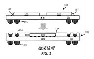
図1は、第1のパッケージ102が第2のパッケージ104に結合されている状態を示す。第1のパッケージ102は、第1の基板106と、第1のダイ(たとえば、チップ)108と、モールド110と、はんだボールの第1のセット116と、配線の第1のセット118と、はんだボールの第3のセット126とを含む。第1の基板106は、トレースおよび/またはビア(どちらも図示されていない)を含んでもよい。第2のパッケージ104は、第2の基板105と、第2のダイ107と、第3のダイ109と、はんだボールの第2のセット115と、ワイヤボンディングの第1のセット117と、ワイヤボンディングの第2のセット119とを含む。第2の基板105は、トレースおよび/またはビア(どちらも図示されていない)を含んでもよい。第2のパッケージ104は、第1のパッケージ102よりも上方に位置する。
FIG. 1 shows a state in which the
第1のダイ108は、配線の第1のセット118を通して第1の基板106の第1の表面(たとえば、上面)に結合される。モールド110は、第1のダイ108および配線の第1のセット118を封止する。はんだボールの第1のセット116は、第1の基板106の第2の表面(たとえば、底面)に結合される。はんだボールの第3のセット126は、第1の基板106の第1の表面(たとえば、上面)に結合される。はんだボールの第3のセット126は、モールド110に囲まれる。第1の基板106は、第1のダイ108および/またははんだボールの第1のセット116に電気的に接続されてもよいトレースおよび/またはビアのセットを含む。
The
第2のダイ107および第3のダイ109は、第2の基板105の第1の表面(たとえば、上面)に結合される。第2のダイ107は、ワイヤボンディングの第1のセット117を通して第2の基板105のトレースおよび/またはビアに電気的に結合される。第3のダイ109は、ワイヤボンディングの第2のセット119を通して第2の基板105のトレースおよび/またはビアに電気的に結合される。はんだボールの第2のセット115は、第2の基板105の第2の表面(たとえば、底面)に結合される。
Second die 107 and third die 109 are coupled to a first surface (eg, an upper surface) of
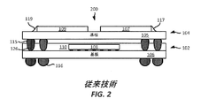
図2は、従来のパッケージオンパッケージ(PoP,package on package)集積デバイスを示す。図2に示すように、集積デバイス200は、図1の第1のパッケージ102と第2のパッケージ104とを含む。図2に示すように、第1のパッケージ102が第2のパッケージ104に結合される場合、第2のパッケージ104のはんだボールの第2のセット115は、第1のパッケージ102のはんだボールの第3のセット126に結合される。
FIG. 2 illustrates a conventional package on package (PoP) integrated device. As shown in FIG. 2, the integrated
図1および図2に示すパッケージオンパッケージ(PoP)構成の1つの主要な欠点は、モバイルコンピューティングデバイスの要件に対して大きすぎる場合がある形状因子を有する集積デバイスが作製されることである。すなわち、図2に示すPoP構成は厚すぎ、ならびに/あるいはモバイルコンピューティングデバイスの要件および/または必要条件を満たすことができないほど大きすぎる表面積を有する場合がある。特に、集積デバイス、特にモバイルデバイスに実装されることになる集積デバイスのサイズを縮小することが常に要求されている。さらに、PoP構成を製作するプロセスは複雑でありコストがかかる場合がある。 One major drawback of the package-on-package (PoP) configuration shown in FIGS. 1 and 2 is that an integrated device is created that has a form factor that may be too large for the requirements of a mobile computing device. That is, the PoP configuration shown in FIG. 2 may be too thick and / or have a surface area that is too large to meet the requirements and / or requirements of a mobile computing device. In particular, there is a constant need to reduce the size of integrated devices that will be implemented in integrated devices, particularly mobile devices. Further, the process of making a PoP configuration can be complex and costly.
したがって、改善された形状因子(たとえば、より小さい、より狭い、より薄い)を有するコスト効果的な集積パッケージが必要である。理想的には、そのような集積パッケージは、現在の集積パッケージと比較して、より高密度の接続を実現するとともに、製作に関してよりコスト効果的である(たとえば、より安価である)。 Thus, there is a need for a cost effective integrated package with improved form factor (eg, smaller, narrower, thinner). Ideally, such an integrated package provides a higher density connection and is more cost effective (e.g., less expensive) to manufacture than current integrated packages.
本明細書において説明する様々な特徴、装置、および方法は、封止層を横切るサイドバリア層を有するビアを含む集積デバイスを提供する。 Various features, apparatus, and methods described herein provide an integrated device that includes a via having a side barrier layer across a sealing layer.
第1の例は、封止層と、封止層を横切るビア構造と、パッドとを含む集積デバイスを提供する。ビア構造は、第1の側面と、第2の側面と、第3の側面とを含むビアを含む。ビア構造は、ビアの少なくとも第1の側面と第3の側面を囲むバリア層も含む。パッドは、ビア構造のバリア層に直接結合される。 The first example provides an integrated device that includes a sealing layer, a via structure across the sealing layer, and a pad. The via structure includes a via that includes a first side, a second side, and a third side. The via structure also includes a barrier layer surrounding at least the first and third sides of the via. The pad is directly coupled to the barrier layer of the via structure.
一態様によれば、集積デバイスは、封止層の第1の表面に結合された第1の誘電体層を含む。いくつかの実装形態では、集積デバイスは、封止層の第2の表面に結合された第2の誘電体層を含む。 According to one aspect, the integrated device includes a first dielectric layer coupled to the first surface of the encapsulation layer. In some implementations, the integrated device includes a second dielectric layer coupled to the second surface of the encapsulation layer.
一態様によれば、集積デバイスは、封止層の第1の表面に結合された基板を含む。いくつかの実装形態では、集積デバイスは、基板に結合された第1のダイを含み、封止層は、第1のダイを封止する。いくつかの実装形態では、ビア構造は充填材をさらに含む。 According to one aspect, the integrated device includes a substrate coupled to the first surface of the encapsulation layer. In some implementations, the integrated device includes a first die coupled to the substrate, and the encapsulation layer encapsulates the first die. In some implementations, the via structure further includes a filler.
一態様によれば、ビアは、シード層を含む。 According to one aspect, the via includes a seed layer.
一態様によれば、ビアは、パッドとして動作するように構成された部分を含む。 According to one aspect, the via includes a portion configured to operate as a pad.
一態様によれば、集積デバイスは、少なくともインターポーザ、パッケージデバイス、および/またはパッケージオンパッケージ(PoP)デバイスのうちの1つを含む。 According to one aspect, the integrated device includes at least one of an interposer, a package device, and / or a package on package (PoP) device.
一態様によれば、集積デバイスは、音楽プレーヤ、ビデオプレーヤ、エンターテイメントユニット、ナビゲーションデバイス、通信デバイス、モバイルデバイス、モバイルフォン、スマートフォン、携帯情報端末、固定位置端末、タブレットコンピュータ、および/またはラップトップコンピュータのうちの少なくとも1つに組み込まれる。 According to one aspect, the integrated device is a music player, video player, entertainment unit, navigation device, communication device, mobile device, mobile phone, smartphone, personal digital assistant, fixed location terminal, tablet computer, and / or laptop computer. In at least one of the above.
第2の例は、封止層と、封止層を横切るビア構造と、パッドとを含む装置を提供する。ビア構造は、第1の側面と、第2の側面と、第3の側面とを含むビアを含む。ビア構造は、ビアの少なくとも第1の側面と第3の側面を囲むバリア手段を含む。パッドは、ビア構造のバリア層に直接結合される。 The second example provides a device that includes a sealing layer, a via structure across the sealing layer, and a pad. The via structure includes a via that includes a first side, a second side, and a third side. The via structure includes barrier means surrounding at least the first and third sides of the via. The pad is directly coupled to the barrier layer of the via structure.
一態様によれば、装置は、封止層の第1の表面に結合された第1の誘電体層を含む。いくつかの実装形態では、装置は、封止層の第2の表面に結合された第2の誘電体層を含む。 According to one aspect, the device includes a first dielectric layer coupled to the first surface of the sealing layer. In some implementations, the device includes a second dielectric layer coupled to the second surface of the sealing layer.
一態様によれば、装置は、封止層の第1の表面に結合された基板を含む。いくつかの実装形態では、装置は、基板に結合された第1のダイを含み、封止層は、第1のダイを封止する。 According to one aspect, the device includes a substrate coupled to the first surface of the sealing layer. In some implementations, the device includes a first die coupled to the substrate, and the encapsulation layer encapsulates the first die.
一態様によれば、ビア構造は充填手段を含む。 According to one aspect, the via structure includes filling means.
一態様によれば、ビアはシード層を含む。 According to one aspect, the via includes a seed layer.
一態様によれば、ビアは、パッドとして動作するように構成された部分を含む。 According to one aspect, the via includes a portion configured to operate as a pad.
一態様によれば、装置は、少なくともインターポーザ、パッケージデバイス、および/またはパッケージオンパッケージ(PoP)デバイスのうちの1つを含む。 According to one aspect, an apparatus includes at least one of an interposer, a package device, and / or a package on package (PoP) device.
一態様によれば、装置は、音楽プレーヤ、ビデオプレーヤ、エンターテイメントユニット、ナビゲーションデバイス、通信デバイス、モバイルデバイス、モバイルフォン、スマートフォン、携帯情報端末、固定位置端末、タブレットコンピュータ、および/またはラップトップコンピュータのうちの少なくとも1つに組み込まれる。 According to one aspect, the apparatus is a music player, video player, entertainment unit, navigation device, communication device, mobile device, mobile phone, smartphone, personal digital assistant, fixed location terminal, tablet computer, and / or laptop computer. Incorporated into at least one of them.
第3の例は、集積デバイスを作製するための方法を提供する。この方法では、基板上にパッドを形成する。この方法では、基板上に封止層を形成する。この方法では、封止層にビア構造を形成し、ビア構造を形成することは、(1)封止層にバリア層を形成することと、(2)バリア層上にビアを形成することであって、ビアが、第1の側面と、第2の側面と、第3の側面とを備え、ビアは、バリア層がビアの少なくとも第1の側面と第3の側面を囲むようにバリア層上に形成され、バリア層はパッドに直接結合される。 The third example provides a method for making an integrated device. In this method, a pad is formed on a substrate. In this method, a sealing layer is formed on the substrate. In this method, a via structure is formed in the sealing layer, and the via structure is formed by (1) forming a barrier layer in the sealing layer and (2) forming a via on the barrier layer. The via includes a first side, a second side, and a third side, and the via has a barrier layer such that the barrier layer surrounds at least the first side and the third side of the via. Formed thereon, the barrier layer is bonded directly to the pad.
一態様によれば、この方法では、封止層の第1の表面上に第1の誘電体層を形成する。 According to one aspect, the method forms a first dielectric layer on the first surface of the encapsulation layer.
一態様によれば、この方法では、封止層の第2の表面上に第2の誘電体層を形成する。 According to one aspect, the method forms a second dielectric layer on the second surface of the sealing layer.
一態様によれば、この方法では基板の少なくとも一部を除去する。 According to one aspect, the method removes at least a portion of the substrate.
一態様によれば、この方法では、基板に第1のダイを結合し、封止層を形成することは、第1のダイを封止層によって封止することを含む。 According to one aspect, in this method, bonding the first die to the substrate and forming the sealing layer includes sealing the first die with the sealing layer.
一態様によれば、ビア構造を形成することは充填材を形成することを含む。 According to one aspect, forming the via structure includes forming a filler.
一態様によれば、ビアを形成することは、バリア層上にシード層を形成することを含む。 According to one aspect, forming the via includes forming a seed layer on the barrier layer.
一態様によれば、ビアを形成することは、ビアの一部をパッドとして形成することを含む。 According to one aspect, forming the via includes forming a portion of the via as a pad.
一態様によれば、集積デバイスは、少なくともインターポーザ、パッケージデバイス、および/またはパッケージオンパッケージ(PoP)デバイスのうちの1つを備える。 According to one aspect, the integrated device comprises at least one of an interposer, a package device, and / or a package on package (PoP) device.
一態様によれば、集積デバイスは、音楽プレーヤ、ビデオプレーヤ、エンターテイメントユニット、ナビゲーションデバイス、通信デバイス、モバイルデバイス、モバイルフォン、スマートフォン、携帯情報端末、固定位置端末、タブレットコンピュータ、および/またはラップトップコンピュータのうちの少なくとも1つに組み込まれる。 According to one aspect, the integrated device is a music player, video player, entertainment unit, navigation device, communication device, mobile device, mobile phone, smartphone, personal digital assistant, fixed location terminal, tablet computer, and / or laptop computer. In at least one of the above.
様々な特徴、性質、および利点は、同様の参照符号が全体にわたって対応して識別する図面と併せて読まれたとき、以下に記載する詳細な説明から明らかになる場合がある。 Various features, characteristics and advantages may become apparent from the detailed description set forth below when read in conjunction with the drawings in which like reference characters identify correspondingly throughout.
以下の説明では、本開示の様々な態様を完全に理解することが可能なように具体的な詳細を示す。しかしながら、それらの態様が、これらの具体的な詳細なしに実施でき得ることが、当業者には理解されよう。たとえば、態様を不必要に詳しく説明して曖昧にすることを避けるために、回路がブロック図で示される場合がある。他の例では、本開示の態様を曖昧にしないように、周知の回路、構造、および技術は詳細には示されていない場合がある。 In the following description, specific details are set forth to provide a thorough understanding of various aspects of the disclosure. However, those skilled in the art will appreciate that the embodiments may be practiced without these specific details. For example, circuitry may be shown in block diagram form in order to avoid unnecessarily elaborating and obscuring aspects. In other instances, well-known circuits, structures, and techniques may not be shown in detail in order not to obscure aspects of the present disclosure.
概説
いくつかの新規の特徴は、封止層と、封止層を横切るビア構造と、パッドとを含む集積デバイスに関する。ビア構造は、第1の側面と、第2の側面と、第3の側面とを含むビアを含む。ビア構造は、ビアの少なくとも第1の側面と第3の側面を囲むバリア層も含む。パッドは、ビア構造のバリア層に直接結合される。いくつかの実装形態では、ビア構造は充填材(たとえば、ポリマー充填材)も含む。いくつかの実装形態では、集積デバイスは、封止層の第1の表面に結合された第1の誘電体層を含む。いくつかの実装形態では、集積デバイスは、封止層の第2の表面に結合された第2の誘電体層を含む。いくつかの実装形態では、集積デバイスは、封止層の第1の表面に結合された基板を含む。いくつかの実装形態では、集積デバイスは、基板に結合された第1のダイを含み、封止層は、第1のダイを封止する。いくつかの実装形態では、基板は基板貫通ビア(TSV,through substrate via)のセットを含む。いくつかの実装形態では、ビアはシード層を含む。いくつかの実装形態では、ビアは、パッドとして動作するように構成された部分を含む。
Overview Some novel features relate to an integrated device that includes a sealing layer, a via structure across the sealing layer, and a pad. The via structure includes a via that includes a first side, a second side, and a third side. The via structure also includes a barrier layer surrounding at least the first and third sides of the via. The pad is directly coupled to the barrier layer of the via structure. In some implementations, the via structure also includes a filler (eg, a polymer filler). In some implementations, the integrated device includes a first dielectric layer coupled to the first surface of the encapsulation layer. In some implementations, the integrated device includes a second dielectric layer coupled to the second surface of the encapsulation layer. In some implementations, the integrated device includes a substrate coupled to the first surface of the encapsulation layer. In some implementations, the integrated device includes a first die coupled to the substrate, and the encapsulation layer encapsulates the first die. In some implementations, the substrate includes a set of through-substrate vias (TSVs). In some implementations, the via includes a seed layer. In some implementations, the via includes a portion configured to operate as a pad.
封止層を横切るサイドバリア層を有するビアを含む例示的な集積デバイス
図3は、集積デバイス(たとえば、パッケージデバイス、パッケージオンパッケージ(PoP)デバイス、インターポーザ)に実装されてもよい封止貫通ビア(TEV)のセットの一例を示す。
Exemplary Integrated Device Comprising Vias with Side Barrier Layers Across the Encapsulating Layer FIG. 3 illustrates a sealed through via that may be implemented in an integrated device (eg, package device, package on package (PoP) device, interposer). An example of a set of (TEV) is shown.
詳細には、図3は、基板302と、絶縁層304と、封止層306と、誘電体層308とを示す。図3はまた、第1のパッド310と、第1のバリア層312と、封止貫通ビア(TEV)314と、キャビティ315とを示す。第1のパッド310は、基板302内に配置される。各実装形態は、基板302用のそれぞれに異なる材料を使用してもよい(たとえば、シリコン、ガラス、セラミック、有機物)。いくつかの実装形態では、基板302はウエハレベル基板である。
Specifically, FIG. 3 shows a
第1のパッド310は金属材料(たとえば、アルミニウム)である。絶縁層304は基板302の第1の表面(たとえば、上面)に結合される。いくつかの実装形態では、絶縁層304はパッシベーション層である。いくつかの実装形態では、絶縁層304は誘電体である。いくつかの実装形態では、絶縁層304は第1のパッド310を少なくとも部分的に覆う。各実装形態は、絶縁層304用にそれぞれに異なる材料を使用してもよい(たとえば、それぞれに異なる誘電材料)。いくつかの実装形態では、絶縁層304は窒化ケイ素(SiN)層である。
The
いくつかの実装形態では、封止層306は絶縁層304に結合される。たとえば、封止層306の第1の表面(たとえば、底面)は、絶縁層304の第2の表面(たとえば、上面)に結合される。各実装形態は、封止層306用にそれぞれに異なる材料を使用してもよい。いくつかの実装形態では、封止層306は充填材ム層である。いくつかの実装形態では、封止層306は、光パターニング可能特性を有する材料で作られる。いくつかの実装形態では、封止層306は、フォトエッチングプロセスによって除去する(たとえば、エッチングする)ことができる材料で作られる。いくつかの実装形態では、封止層306にフォトエッチングプロセスを施すと、TEVを形成するプロセスにおいて封止層306にキャビティを形成する(たとえば、作製する)際にパッケージの他の構成要素が損傷を受けないようになる。たとえば、いくつかの実装形態では、光パターニング可能な封止層306に対してフォトエッチングプロセスを使用すると、レーザを使用して封止層306にキャビティを作製する場合にあり得るパッド310の損傷が回避される。たとえば、レーザプロセスを使用してパッド(たとえば、パッド310)の上方の封止層にキャビティを作製すると、レーザがパッド(たとえば、パッド310)を損傷しならびに/あるいは破壊し、それによってTEVが基板の配線に適切に結合されるのを妨げる。
In some implementations, the
第1のバリア層312およびTEV 314は、封止層306内に配置される。TEV 314は、封止層306を横切る金属層(たとえば、銅)である。いくつかの実装形態では、TEV 314はシード層を含む。そのような場合、TEV 314は金属層(たとえば、銅層)とシード層とを含む。いくつかの実装形態では、シード層は、TEV 314の金属層とバリア層312との間に位置する。TEV 314は、第1の側面(たとえば、下側面)と、第2の側面(たとえば、上側面)と、第3の側面(たとえば、垂直側面)とを有する。いくつかの実装形態では、TEV 314の第3の側面はTEV 314の壁であってもよい。いくつかの実装形態では、TEV 314は非水平側面を有してもよい。たとえば、TEV 314は、非垂直側面または非水平側面(たとえば、対角側面)を有してもよい。
The
図3に示すように、第1のバリア層312がTEV 314に結合される。特に、TEV 314は封止層306内で第1のバリア層312に囲まれる。第1のバリア層312は、TEV 314の第1の側面およびTEV 314の第3の側面(たとえば、垂直側面)に結合される。したがって、図3に示すように、いくつかの実装形態では、TEV 314が封止層306に直接接触することはない(たとえば、直接的な接点を有さない)。各実装形態は、第1のバリア層312用にそれぞれに異なる材料を使用してもよい。いくつかの実装形態では、第1のバリア層312は、少なくともチタン(Ti)、TiN、および/またはTiWのうちの1つである。しかし、第1のバリア層312は、他の材料であってもよく、列挙された材料に限定されない。
As shown in FIG. 3, a
第1のバリア層312は、第1のパッド310に結合される。いくつかの実装形態では、第1のバリア層312は絶縁層304に少なくとも部分的に囲まれる。
The
誘電体層308は封止層306に結合される。いくつかの実装形態では、誘電体層308の第1の表面(たとえば、底面)は、封止層306の第2の表面(たとえば、上面)に結合される。いくつかの実装形態では、誘電体層308の第2の表面(たとえば、上面)は、TEV 314の上面に揃えてもよい。いくつかの実装形態では、誘電体層308は、誘電体層308を開放し、TEV 314の上面の一部を露出させるキャビティ315を含んでもよい。
図3に示すように、TEV 314は、TEV 314がビアとパッドの両方であるように構成される。いくつかの実装形態では、ビアとパッドの組合せをビア構造と呼ぶことがある。いくつかの実装形態では、ビア構造はTEV 314と第1のバリア層312とを含む。いくつかの実装形態では、TEV 314はT字形を有する。いくつかの実装形態では、第1のバリア層312はU字形を有する。
As shown in FIG. 3, TEV 314 is configured such that TEV 314 is both a via and a pad. In some implementations, the combination of vias and pads may be referred to as a via structure. In some implementations, the via structure includes a TEV 314 and a
図3に示すように第1のバリア層312とTEV 314とを含むビア構造が、様々な集積デバイスに実装されてもよい。いくつかの実装形態では、ビア構造は、集積パッケージデバイス(たとえば、パッケージオンパッケージ(PoP)デバイス)に実装されてもよい。
A via structure including a
図3は、第1のパッド310が基板302に埋め込まれることを示す。しかし、いくつかの実装形態では、第1のパッド310は、基板302の表面上に配置される。
FIG. 3 shows that the
図4は、ビア構造401のセットを含む集積パッケージデバイス400を示す。いくつかの実装形態では、ビア構造401は、図3に示すビア構造および/または本開示において説明し図示する任意の新規のビア構造であってもよい。
FIG. 4 shows an
図4に示すように、集積パッケージデバイス400は、基板402と、第1のダイ404と、第2のダイ406と、配線の第1のセット414と、配線の第2のセット416と、封止層418と、第1の誘電体層420と、第2の誘電体層422と、基板貫通ビア(TSV)のセット424と、配線の第3のセット426と、はんだボールのセット428と、第1のパッド430とを含む。いくつかの実装形態では、基板402は、図を明確にするために示されていない配線(たとえば、トレース、ビア)のセットを含んでもよい。配線のセットは、1つまたは複数のパッド(たとえば、パッド430)および/または配線の第3のセット426に結合されてもよい。
As shown in FIG. 4, the
第1のダイ404は、配線の第1のセット414(たとえば、第1のバンプ、第1のピラー配線、第1のはんだ)を通して基板402に結合される。第2のダイ406は、配線の第2のセット416(たとえば、第2のバンプ、第2のピラー配線、第2のはんだ)を通して基板402に結合される。封止層418は第1のダイ404および第2のダイ406を覆う。
The
ビア構造401のセットは、封止層418を横切り、基板402に結合される。いくつかの実装形態では、ビア構造のセット401は少なくとも第1のパッド430に結合される。いくつかの実装形態では、第1のパッド430は、TSVのセット424のうちの少なくとも1つのTSVに結合される。TSVのセット424のTSVのうちの少なくとも1つのTSVが、配線426の第3のセットに結合されてもよい。配線の第3のセット426のうちの少なくとも1つの配線が、はんだボールのセット428のうちのはんだボールに結合されてもよい。
A set of via
いくつかの実装形態では、基板402の第1の表面上に誘電体層409が結合される(たとえば、形成される)。いくつかの実装形態では、誘電体層409は、絶縁層304と同様でありならびに/あるいは同じである。いくつかの実装形態では、封止層418は誘電体層409に結合される。
In some implementations, a
ビア構造401のうちの1つは、第1のバリア層403(たとえば、第1のバリア層312)と封止貫通ビア(TEV)405(たとえば、TEV 314)とを含む。第1のバリア層403およびTEV 405は、封止層418内に配置される。TEV 405は、封止層418を横切る金属層(たとえば、銅)である。いくつかの実装形態では、TEV 405はシード層を含む。そのような場合、TEV 405は金属層(たとえば、銅層)とシード層とを含む。いくつかの実装形態では、シード層は、TEV 405の金属層とバリア層403との間に位置する。TEV 405は、第1の側面(たとえば、下側面)と、第2の側面(たとえば、上側面)と、第3の側面(たとえば、垂直側面)とを有する。いくつかの実装形態では、TEV 405の第3の側面はTEV 405の壁であってもよい。いくつかの実装形態では、TEV 405の垂直側面は、封止層418の上面および/または底面に垂直である。
One of the via
第1のバリア層403は、TEV 405に結合される。特に、TEV 405は封止層418内で第1のバリア層403に囲まれる。第1のバリア層403は、TEV 405の第1の側面およびTEV 405の第3の側面(たとえば、垂直側面)に結合される。したがって、図4に示すように、いくつかの実装形態では、TEV 405が封止層418に直接接触することはない(たとえば、直接的な接点を有さない)。
The
図4は、第1のパッド430が基板402に埋め込まれることを示す。しかし、いくつかの実装形態では、第1のパッド430は、基板402の表面上に配置される。図を明確にするために図4には示されていないが、第1のパッド430は基板402内の配線(たとえば、ビア、トレース)に結合される。
FIG. 4 shows that the
いくつかの実装形態では、集積デバイス400は、パッケージオンパッケージ(PoP)集積デバイスにおけるパッケージ(たとえば、集積デバイス)である。したがって、いくつかの実装形態では、別の集積デバイス(たとえば、別のパッケージ)が集積デバイス400に結合されてもよい。たとえば、基板と配線(たとえば、はんだボール)とを備える別の集積デバイスが集積デバイス400の上部に結合されてもよい。そのような場合、配線(たとえば、はんだボール)は、集積デバイス400のビア構造401に結合されてもよい。
In some implementations, the
封止層を横切るサイドバリア層を有するビアを含む集積デバイスを提供/製作する例示的なシーケンス
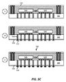
いくつかの実装形態では、ビア構造を含む集積デバイス(たとえば、集積パッケージ)を提供することは、いくつかのプロセスを含む。図5(図5A〜図5Cを含む)は、集積デバイスを提供するための例示的なシーケンスを示す。いくつかの実装形態では、図5A〜図5Cのシーケンスは、図3および/または図4の集積デバイス、ならびに/あるいは本開示で説明する他の集積デバイスを提供する/製造するために使用され得る。
Exemplary Sequences for Providing / Manufacturing Integrated Devices Containing Vias with Side Barrier Layers Across the Encapsulation Layer In some implementations, providing an integrated device (eg, an integrated package) that includes a via structure is Process. FIG. 5 (including FIGS. 5A-5C) illustrates an exemplary sequence for providing an integrated device. In some implementations, the sequence of FIGS. 5A-5C may be used to provide / manufacture the integrated device of FIGS. 3 and / or 4 and / or other integrated devices described in this disclosure. .
図5A〜図5Cのシーケンスが、回路要素も含む集積デバイスを提供する/製造するために使用されてもよいことにも留意されたい。図5A〜図5Cのシーケンスが、集積デバイスを提供するためのシーケンスを簡略化しならびに/あるいは明確化するために1つまたは複数の段階を組み合わせてもよいことにさらに留意されたい。 Note also that the sequence of FIGS. 5A-5C may be used to provide / manufacture an integrated device that also includes circuit elements. It is further noted that the sequence of FIGS. 5A-5C may combine one or more stages to simplify and / or clarify the sequence for providing an integrated device.
いくつかの実装形態では、図5A〜図5Cのプロセスは、高密度配線を有する集積デバイスを提供する新規のプロセスを示す。 In some implementations, the processes of FIGS. 5A-5C illustrate a novel process for providing an integrated device with high density wiring.
図5Aの段階1において示すように、基板502を設ける(たとえば、製作する)。いくつかの実装形態では、基板502はウエハである。各実装形態では、基板用にそれぞれに異なる様々な材料を使用してもよい(たとえば、シリコン基板、ガラス基板、セラミック基板、有機基板)。基板502は、基板貫通ビア(TSV)のセット504とパッドのセット505とを含む。いくつかの実装形態では、基板502は他の配線(たとえば、トレース)を含んでもよい。パッドのセット505は、基板502の第1の表面(たとえば、上面)上に配置される。いくつかの実装形態では、パッドのセット505は、基板502の第1の表面に埋め込まれる。いくつかの実装形態では、基板502の第1の表面上に誘電体層503が結合される(たとえば、形成される)。いくつかの実装形態では、誘電体層503は、絶縁層304と同様でありならびに/あるいは同じである。誘電体層503は、1つまたは複数のパッド505および/またはTSVの1つまたは複数のセット504の上方に1つまたは複数の開口部および/またはキャビティを含んでもよい。いくつかの実装形態では、基板502は、図を明確にするために示されていない配線(たとえば、トレース、ビア)のセットを含んでもよい。配線のセットは、1つまたは複数のパッド(たとえば、パッド505)に結合されてもよい。
As shown in
段階2において、基板502に第1のダイ506および第2のダイ508を結合する。第1のダイ506を配線の第1のセット516(たとえば、第1のピラー、第1のはんだ)を通して基板502に結合する。いくつかの実装形態では、配線の第1のセットのうちの少なくとも1つの配線がTSVのセット504のうちの少なくとも1つのTSVに電気的に結合される。第2のダイ508は、配線の第2のセット518(たとえば、第1のピラー、第1のはんだ)を通して基板502に結合される。いくつかの実装形態では、配線の第2のセット518のうちの少なくとも1つの配線をTSVのセット504のうちの少なくとも1つのTSVに電気的に結合する。
In
段階3において、基板502上および/または基板502上の誘電体層503上に封止層520を設ける(たとえば、形成する)。封止層520は、第1のダイ506および第2のダイ508を封止する。いくつかの実装形態では、封止層520は基板502に直接結合されてもよい。各実装形態は、封止層520用にそれぞれに異なる材料を使用してもよい。いくつかの実装形態では、封止層520は充填材ム層である。いくつかの実装形態では、封止層520は、光パターニング可能特性を有する材料で作られる。
In
段階4において、封止層520にキャビティ525を形成する。いくつかの実装形態では、キャビティ525はパッド(たとえば、パッド505)の上方に形成される(たとえば、作製される)。いくつかの実装形態では、キャビティ525は、フォトエッチングプロセス(たとえば、フォトリソグラフィプロセス)を使用することによって形成される。
In
段階5において、バリア層530を設ける(たとえば、形成する、堆積させる)。いくつかの実装形態では、バリア層530を形成するためにめっきプロセスが使用される。バリア層530は、キャビティ525の内壁、パッド505の少なくとも一部、および/または封止層520の第1の表面を覆ってもよい。各実装形態は、バリア層530用にそれぞれに異なる材料を使用してもよい。いくつかの実装形態では、バリア層530は、少なくともチタン(Ti)、(TiN)、アルミニウム銅(AlCu)、チタン銅合金(TiCu)、および/またはチタンタングステン銅合金(TiWCu)のうちの1つである。しかしながら、各実装形態は、それぞれに異なる材料を使用してもよい。したがって、バリア層530用の材料を上記に記載した材料に限定すべきではない。
In
バリア層530上にシード層532も設ける(たとえば、形成する、堆積させる)。いくつかの実装形態では、バリア層530上にシード層532を形成するためにめっきプロセスが使用される。各実装形態は、シード層532用にそれぞれに異なる材料を使用してもよい。いくつかの実装形態では、シード層532は金属層である。
A
段階6において、シード層532上にフォトレジスト層534を設ける(たとえば、形成する、堆積させる)。いくつかの実装形態では、フォトレジスト層534を設けることは、フォトレジスト層534を設けることと、フォトレジスト層534のいくつかの部分を選択的に除去することとを含む。
In
段階7において、シード層532上に金属層536を設ける(たとえば、形成する、堆積させる)。いくつかの実装形態では、金属層536は、フォトレジスト層534によって覆われていないシード層532上に設けられる。いくつかの実装形態では、シード層532上に金属層536を設けるためにリソグラフィおよびめっきプロセスが使用される。いくつかの実装形態では、金属層536とシード層532は同じ材料である。したがって、いくつかの実装形態では、金属層536はシード層532を含んでもよい。
In
段階8において、フォトレジスト層534、シード層532、およびバリア層530を選択的に除去する(たとえば、エッチングする)。いくつかの実装形態では、フォトレジスト層534、シード層532、およびバリア層530を同時に除去する。いくつかの実装形態では、フォトレジスト層534、シード層532、およびバリア層530を順次除去する。段階8に示すように、フォトレジスト層534、シード層532、およびバリア層530を選択的に除去した後にビア構造538を製作する。いくつかの実装形態では、ビア構造538は、図3〜図4に記載されたビア構造のうちの1つである。
In
段階9において、場合によっては、封止層520の第2の表面上に誘電体層540を設ける(たとえば、形成する)。いくつかの実装形態では、誘電体層540の表面をビア構造538の表面と揃える。いくつかの実装形態では、誘電体層540はビア構造538を覆ってもよく、ビア構造538の一部の上方にキャビティを形成してもよい。
In step 9, a
段階10において、場合によっては、基板502の第2の表面(たとえば、底面)上に別の誘電体層550を設ける(たとえば、形成する)。さらに、誘電体層550上/内に配線のセット552も設ける。いくつかの実装形態では、配線のセット552は、再分配層および/またはアンダーバンプメタライゼーション(UBM)層の少なくとも一方を含む。いくつかの実装形態では、配線のセット552のうちの少なくとも1つの配線をTSVのセット504のうちの少なくとも1つのTSVに電気的に結合する。
In
段階11において、配線のセット552にはんだボールのセット554を結合する。いくつかの実装形態では、段階10の後、封止層と、サイドバリア層を含むビア構造とを含む集積デバイス560を製作する。
In
封止層を横切るサイドバリア層を有するビアを含む例示的な集積デバイス
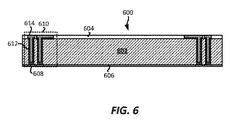
図6は、ビア構造のセット610を含む集積パッケージデバイスを示す。詳細には、図6は、ビア構造のセット610を含むインターポーザ600の一例を示す。いくつかの実装形態では、ビア構造610は、図3に示すビア構造および/または本開示において説明し図示する任意の新規のビア構造であってもよい。
Exemplary Integrated Device Comprising Vias with Side Barrier Layers Across the Encapsulation Layer FIG. 6 illustrates an integrated package device that includes a
図6に示すように、インターポーザ600は、封止層602と、第1の誘電体層604と、基板606と、第1のパッド608と、ビア構造のセット610とを含む。第1の誘電体層604は、封止層602の第1の表面(たとえば、上面)に結合される。基板606は、封止層602の第2の表面(たとえば、底面)に結合される。いくつかの実装形態では、基板606と封止層602の第2の表面との間に第2の誘電体層(たとえば、封止層304)を位置させてもよい。
As shown in FIG. 6, the
ビア構造のセット610は、封止層602を横切る。いくつかの実装形態では、ビア構造のセット610は少なくとも第1のパッド608に結合される。ビア構造610のうちの1つは、少なくともバリア層612と封止貫通ビア(TEV)614とを含む。バリア層612およびTEV 614は封止層602内に配置される。いくつかの実装形態では、バリア層612はパッド608に結合される(たとえば、直接接触する)。TEV 614は、封止層602を横切る金属層(たとえば、銅)である。いくつかの実装形態では、TEV 614はシード層を含む。そのような場合、TEV 614は金属層(たとえば、銅層)とシード層とを含む。いくつかの実装形態では、シード層は、TEV 614の金属層とバリア層612との間に位置する。TEV 614は、第1の側面(たとえば、下側面)と、第2の側面(たとえば、上側面)と、第3の側面(たとえば、垂直側面)とを有する。いくつかの実装形態では、TEV 614の第3の側面はTEV 614の壁であってもよい。いくつかの実装形態では、TEV 614の垂直側面は、封止層602の上面および/または底面に垂直である。
A set of via
バリア層612はTEV 614に結合される。特に、TEV 614は封止層602内でバリア層612に囲まれる。バリア層612は、TEV 614の第1の側面およびTEV 614の垂直側面に結合される。したがって、図6に示すように、いくつかの実装形態では、TEV 614が封止層602に直接接触することはない(たとえば、直接的な接点を有さない)。
封止層を横切るサイドバリア層を有するビアを含む集積デバイスを提供/製作する例示的なシーケンス
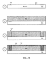
いくつかの実装形態では、集積デバイスはインターポーザを含んでもよい。いくつかの実装形態では、ビア構造を含む集積デバイス(たとえば、集積パッケージ)を提供することは、いくつかのプロセスを含む。図7(図7A〜図7Cを含む)は、集積デバイスを提供するための例示的なシーケンスを示す。いくつかの実装形態では、図7A〜図7Cのシーケンスは、図3、図4、および/または図6の集積デバイス、ならびに/あるいは本開示において説明する他の集積デバイスを提供する/製造するために使用されてもよい。
Exemplary Sequence for Providing / Manufacturing an Integrated Device Comprising a Via With a Side Barrier Layer Across a Sealing Layer In some implementations, the integrated device may include an interposer. In some implementations, providing an integrated device (eg, an integrated package) that includes a via structure includes a number of processes. FIG. 7 (including FIGS. 7A-7C) illustrates an exemplary sequence for providing an integrated device. In some implementations, the sequence of FIGS. 7A-7C provides / manufactures the integrated devices of FIGS. 3, 4, and / or 6 and / or other integrated devices described in this disclosure. May be used.
図7A〜図7Cのシーケンスが、集積デバイスを提供するためのシーケンスを簡略化しならびに/あるいは明確化するために1つまたは複数の段階を組み合わせてもよいことにさらに留意されたい。 It should further be noted that the sequence of FIGS. 7A-7C may combine one or more stages to simplify and / or clarify the sequence for providing an integrated device.
いくつかの実装形態では、図7A〜図7Cのプロセスは、高密度配線を有する集積デバイス(たとえば、インターポーザ)を提供する新規のプロセスを示す。 In some implementations, the processes of FIGS. 7A-7C illustrate a novel process for providing an integrated device (eg, an interposer) with high density wiring.
図7Aの段階1において示すように、キャリア702を設ける(たとえば、製作する)。いくつかの実装形態では、キャリア702は、少なくとも基板および/またはウエハの一方である。各実装形態では、キャリア用にそれぞれに異なる様々な材料を使用してもよい(たとえば、シリコン基板、ガラス基板、セラミック基板、有機基板)。キャリア702は、パッドのセット705を含む。いくつかの実装形態では、キャリア702は他の配線(たとえば、トレース)を含んでもよい。パッドのセット705は、キャリア702の第1の表面(たとえば、上面)に埋め込まれる。いくつかの実装形態では、パッドのセット705はキャリア702の第1の表面(たとえば、上面)上に配置される。いくつかの実装形態では、基板704の第1の表面上に誘電体層703が結合される(たとえば、形成される)。いくつかの実装形態では、誘電体層は、絶縁層304と同様でありならびに/あるいは同じである。
As shown in
段階2において、キャリア702上および/またはキャリア702上の誘電体層703上に封止層720を設ける(たとえば、形成する)。いくつかの実装形態では、封止層720はパッド705を封止する。いくつかの実装形態では、封止層720はキャリア702に直接結合されてもよい。各実装形態は、封止層720用にそれぞれに異なる材料を使用してもよい。いくつかの実装形態では、封止層720は充填材ム層である。いくつかの実装形態では、封止層720は、光パターニング可能特性を有する材料で作られる。いくつかの実装形態では、封止層720は、フォトエッチングプロセスによって除去する(たとえば、エッチングする)ことができる材料で作られる。
In
段階3において、封止層720内に少なくとも1つのキャビティ725を形成する。いくつかの実装形態では、キャビティ725はパッド(たとえば、パッド705)の上方に形成される(たとえば、作製される)。いくつかの実装形態では、キャビティ725は、フォトエッチングプロセス(たとえば、フォトリソグラフィプロセス)を使用することによって形成される。
In
段階4において、バリア層730を設ける(たとえば、形成する、堆積させる)。いくつかの実装形態では、バリア層730を形成するためにめっきプロセスが使用される。バリア層730は、キャビティ725の内壁、パッド705の少なくとも一部、および/または封止層720の第1の表面を覆ってもよい。各実装形態は、バリア層730用にそれぞれに異なる材料を使用してもよい。各実装形態は、バリア層730用にそれぞれに異なる材料を使用してもよい。いくつかの実装形態では、バリア層730は、少なくともチタン(Ti)、(TiN)、アルミニウム銅(AlCu)、チタン銅合金(TiCu)、および/またはチタンタングステン銅合金(TiWCu)のうちの1つである。
In
バリア層730上にシード層732も設ける(たとえば、形成する、堆積させる)。いくつかの実装形態では、バリア層730上にシード層732を形成するためにめっきプロセスが使用される。各実装形態は、シード層732用にそれぞれに異なる材料を使用してもよい。いくつかの実装形態では、シード層732は金属層である。
A
段階5において、シード層732上にフォトレジスト層734を設ける(たとえば、形成する、堆積させる)。いくつかの実装形態では、フォトレジスト層734を設けることは、フォトレジスト層734を設けることと、フォトレジスト層734のいくつかの部分を選択的に除去することとを含む。
In
段階6において、シード層732上に金属層736を設ける(たとえば、形成する、堆積させる)。いくつかの実装形態では、金属層736は、フォトレジスト層734によって覆われていないシード層732上に設けられる。いくつかの実装形態では、シード層732上に金属層736を設けるためにリソグラフィおよびめっきプロセスが使用される。いくつかの実装形態では、金属層736とシード層732は同じ材料である。したがって、いくつかの実装形態では、金属層736はシード層732を含んでもよい。
In
段階7において、フォトレジスト層734、シード層732、およびバリア層730を選択的に除去する(たとえば、エッチングする)。いくつかの実装形態では、フォトレジスト層734、シード層732、およびバリア層730を同時に除去するか、あるいはフォトレジスト層734、シード層732、およびバリア層730を順次除去する。段階7に示すように、フォトレジスト層734、シード層732、およびバリア層730を選択的に除去した後にビア構造738を製作する。いくつかの実装形態では、ビア構造738は、図3〜図4に記載されたビア構造のうちの1つである。
In
段階8において、場合によっては、封止層720の第2の表面上に誘電体層740を設ける(たとえば、形成する)。いくつかの実装形態では、誘電体層740の表面をビア構造738の表面と揃える。いくつかの実装形態では、誘電体層740はビア構造738を覆ってもよく、ビア構造738の一部の上方にキャビティを形成してもよい。
In
段階8において、キャリア702の少なくとも一部を除去する(たとえば、研磨する、研削する、エッチングする)。いくつかの実装形態では、キャリア702は、キャリア702の表面がパッド705の表面と揃えられるまで除去される。いくつかの実装形態では、段階9の後、封止層と、サイドバリア層を含むビア構造とを含む集積デバイス760を製作する。
In
封止層を横切るサイドバリア層と充填材とを有するビアを含む例示的な集積デバイス
図8は、集積デバイス(たとえば、集積パッケージデバイス、パッケージオンパッケージ(PoP)デバイス、インターポーザ)に実装されてもよい封止貫通ビア(TEV)のセットの一例を示す。
Exemplary Integrated Device Comprising Vias with Side Barrier Layers and Fillers Across the Sealing Layer FIG. 8 may also be implemented in an integrated device (eg, integrated package device, package on package (PoP) device, interposer). An example of a set of good through-sealing vias (TEV) is shown.
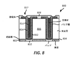
詳細には、図8は、基板802と、絶縁層804と、封止層806と、誘電体層808とを示す。図8はまた、第1のパッド810と、第1のバリア層812と、封止貫通ビア(TEV)814と、充填材816と、キャビティ817とを示す。第1のパッド810は、基板802内に配置される。各実装形態は、基板802用のそれぞれに異なる材料を使用してもよい(たとえば、シリコン、ガラス、セラミック、有機物)。いくつかの実装形態では、基板802はウエハレベル基板である。
Specifically, FIG. 8 shows a substrate 802, an insulating
第1のパッド810は、金属材料(たとえば、アルミニウム)である。絶縁層804は、基板802の第1の表面(たとえば、上面)に結合される。いくつかの実装形態では、絶縁層804はパッシベーション層である。いくつかの実装形態では、絶縁層304は誘電体である。いくつかの実装形態では、絶縁層804は第1のパッド810を少なくとも部分的に覆う。各実装形態は、絶縁層804用にそれぞれに異なる材料を使用してもよい(たとえば、それぞれに異なる誘電材料)。いくつかの実装形態では、絶縁層804は窒化ケイ素(SiN)層である。
The
いくつかの実装形態では、封止層806は絶縁層804に結合される。たとえば、封止層806の第1の表面(たとえば、底面)は、絶縁層804の第2の表面(たとえば、上面)に結合される。各実装形態は、封止層806用にそれぞれに異なる材料を使用してもよい。いくつかの実装形態では、封止層806は充填材ム層である。いくつかの実装形態では、封止層806は、光パターニング可能特性を有する材料で作られる。いくつかの実装形態では、封止層806は、フォトエッチングプロセスによって除去する(たとえば、エッチングする)ことができる材料で作られる。いくつかの実装形態では、封止層806にフォトエッチングプロセスを施すと、TEVを形成するプロセスにおいて封止層806にキャビティを形成する(たとえば、作製する)際にパッケージの他の構成要素が損傷を受けないようになる。たとえば、いくつかの実装形態では、光パターニング可能な封止層806に対してフォトエッチングプロセスを使用すると、レーザを使用して封止層806にキャビティを作製する場合にあり得るパッド810の損傷が回避される。たとえば、レーザプロセスを使用してパッド(たとえば、パッド810)の上方の封止層にキャビティを作製すると、レーザがパッド(たとえば、パッド810)を損傷しならびに/あるいは破壊し、それによってTEVが基板の配線に適切に結合されるのを妨げる。
In some implementations, the
第1のバリア層812、TEV 814、および充填材816は封止層806内に配置される。TEV 814は、封止層806を横切る金属層(たとえば、銅)である。いくつかの実装形態では、TEV 814はシード層を含む。そのような場合、TEV 814は金属層(たとえば、銅層)とシード層とを含む。いくつかの実装形態では、シード層は、TEV 814の金属層とバリア層812との間に位置する。TEV 814は、第1の側面(たとえば、下側面)と、第2の側面(たとえば、上側面)と、第3の側面(たとえば、垂直側面)とを有する。いくつかの実装形態では、TEV 814の第3の側面はTEV 814の壁であってもよい。いくつかの実装形態では、TEV 814は非水平側面を有してもよい。たとえば、TEV 814は、非垂直側面または非水平側面(たとえば、対角側面)を有してもよい。各実装形態では、充填材816にそれぞれに異なる材料を使用してもよい。たとえば、充填材816はポリマー充填材を含んでもよい。いくつかの実装形態では、充填材816はビア構造の構造安定性を実現する。
図8は、TEV 814がバリア層812の形状に整合することを示す。この例では、バリア層812はU字形断面を有する。この例では、TEV 814はU字形断面を有する。図8は、充填材816がTEV 814に結合されることも示す。特に、充填材816はTEV 814に囲まれる。第1のバリア層812はTEV 814に結合される。特に、TEV 814は封止層806内で第1のバリア層812に囲まれる。第1のバリア層812は、TEV 814の第1の側面およびTEV 814の第3の側面(たとえば、垂直側面)に結合される。したがって、図8に示すように、いくつかの実装形態では、TEV 814が封止層806に直接接触することはない(たとえば、直接的な接点を有さない)。各実装形態は、第1のバリア層812用にそれぞれに異なる材料を使用してもよい。いくつかの実装形態では、第1のバリア層812は、少なくともチタン(Ti)、TiN、および/またはTiWのうちの1つである。しかし、第1のバリア層812は、他の材料であってもよく、列挙された材料に限定されない。
FIG. 8 shows that TEV 814 matches the shape of
第1のバリア層812は、第1のパッド810に結合される。いくつかの実装形態では、第1のバリア層812は絶縁層804に少なくとも部分的に囲まれる。
The
誘電体層808は封止層806に結合される。いくつかの実装形態では、誘電体層808の第1の表面(たとえば、底面)は、封止層806の第2の表面(たとえば、上面)に結合される。いくつかの実装形態では、誘電体層808は、誘電体層808を開放し、TEV 814の上面の一部を露出させるキャビティ817を含んでもよい。図8に示すように、キャビティ817はTEV 814のウィング部(たとえば、水平部分)を露出させる。
図8に示すように、TEV 814は、TEVがビアとパッドの両方であるように構成される。いくつかの実装形態では、ビアとパッドの組合せをビア構造と呼ぶことがある。いくつかの実装形態では、ビア構造はTEV 814と第1のバリア層812とを含む。
As shown in FIG. 8, TEV 814 is configured such that TEV is both a via and a pad. In some implementations, the combination of vias and pads may be referred to as a via structure. In some implementations, the via structure includes a TEV 814 and a
図8に示すように第1のバリア層812とTEV 814とを含むビア構造が、様々な集積デバイスに実装されてもよい。いくつかの実装形態では、ビア構造は、集積パッケージデバイス(たとえば、パッケージオンパッケージ(PoP)デバイス)に実装されてもよい。
A via structure including a
図8は、第1のパッド810が基板802に埋め込まれることを示す。しかし、いくつかの実装形態では、第1のパッド810は、基板802の表面上に配置される。
FIG. 8 shows that the
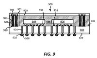
図9は、ビア構造901のセットを含む集積パッケージデバイス900を示す。いくつかの実装形態では、ビア構造901は、図8に示すビア構造および/または本開示において説明し図示する任意の新規のビア構造であってもよい。
FIG. 9 shows an
図9に示すように、集積パッケージデバイス900は、基板902と、第1のダイ904と、第2のダイ906と、誘電体層909と、配線の第1のセット914と、配線の第2のセット916と、封止層918と、第1の誘電体層920と、第2の誘電体層922と、基板貫通ビア(TSV)のセット924と、配線の第3のセット926と、はんだボールのセット928と、第1のパッド930とを含む。いくつかの実装形態では、基板902は、図を明確にするために示されていない配線(たとえば、トレース、ビア)のセットを含んでもよい。配線のセットは、1つまたは複数のパッド(たとえば、パッド930)および/または配線の第3のセット926に結合されてもよい。
As shown in FIG. 9, the
第1のダイ904は、配線の第1のセット914(たとえば、第1のピラー、第1のはんだ)を通して基板902に結合される。第2のダイ906は、配線の第2のセット916(たとえば、第2のピラー、第2のはんだ)を通して基板902に結合される。封止層918は、第1のダイ904および第2のダイ906を覆う。
The
ビア構造901のセットは、封止層918を横切り、基板902に結合される。いくつかの実装形態では、ビア構造のセット901は少なくとも第1のパッド930に結合される。いくつかの実装形態では、第1のパッド930は、TSVのセット924のうちの少なくとも1つのTSVに結合される。TSVのセット924のTSVのうちの少なくとも1つのTSVが、配線926の第3のセットに結合されてもよい。配線の第3のセット926のうちの少なくとも1つの配線が、はんだボールのセット928のうちのはんだボールに結合されてもよい。
The set of via
いくつかの実装形態では、基板902の第1の表面上に誘電体層909が結合される(たとえば、形成される)。いくつかの実施態様では、誘電体層909は、絶縁層804と同様でありならびに/あるいは同じである。いくつかの実装形態では、封止層918は誘電体層909に結合される。
In some implementations, a
ビア構造901のうちの1つは、少なくとも第1のバリア層903(たとえば、第1のバリア層812)と、封止貫通ビア(TEV)905(たとえば、TEV 814)と、充填材907とを含む。第1のバリア層903、TEV 905、および充填材907は、封止層918内に配置される。TEV 905は、封止層918を横切る金属層(たとえば、銅)である。いくつかの実装形態では、TEV 905はシード層を含む。そのような場合、TEV 905は金属層(たとえば、銅層)とシード層とを含む。いくつかの実装形態では、シード層は、TEV 905の金属層とバリア層903との間に位置する。TEV 905は、第1の側面(たとえば、下側面)と、第2の側面(たとえば、上側面)と、第3の側面(たとえば、垂直側面)とを有する。いくつかの実装形態では、TEV 905の第3の側面はTEV 905の壁であってもよい。いくつかの実装形態では、TEV 905の垂直側面は、封止層918の上面および/または底面に垂直である。各実装形態では、充填材907にそれぞれに異なる材料を使用してもよい。たとえば、充填材907はポリマー充填材を含んでもよい。いくつかの実装形態では、充填材907はビア構造901の構造安定性を実現する。
One of the via
第1のバリア層903は、TEV 905に結合される。特に、TEV 905は封止層918内で第1のバリア層903に囲まれる。第1のバリア層903は、TEV 905の第1の側面およびTEV 905の第3の側面(たとえば、垂直側面)に結合される。したがって、図9に示すように、いくつかの実装形態では、TEV 905が封止層918に直接接触することはない(たとえば、直接的な接点を有さない)。いくつかの実装形態では、TEV 905は、第1のバリア層903の形状に整合する。充填材907はTEV 905に囲まれる。
The
図9は、第1のパッド930が基板902に埋め込まれることを示す。しかし、いくつかの実装形態では、第1のパッド930は、基板902の表面上に配置される。図を明確にするために図9には示されていないが、第1のパッド930は基板902内の配線(たとえば、ビア、トレース)に結合される。
FIG. 9 shows that the
いくつかの実装形態では、集積デバイス900は、パッケージオンパッケージ(PoP)集積デバイスにおけるパッケージ(たとえば、集積デバイス)である。したがって、いくつかの実装形態では、別の集積デバイス(たとえば、別のパッケージ)が集積デバイス900に結合されてもよい。たとえば、基板と配線(たとえば、はんだボール)とを備える別の集積デバイスが集積デバイス900の上部に結合されてもよい。そのような場合、配線(たとえば、はんだボール)は、集積デバイス900のビア構造901に結合されてもよい。
In some implementations, the
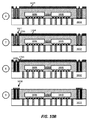
封止層を横切るサイドバリア層と充填材とを有するビアを含む集積デバイスを提供/製作する例示的なシーケンス
いくつかの実装形態では、ビア構造を含む集積デバイス(たとえば、集積パッケージ)を提供することは、いくつかのプロセスを含む。図10(図10A〜図10Cを含む)は、集積デバイスを提供するための例示的なシーケンスを示す。いくつかの実装形態では、図10A〜図10Cのシーケンスは、図8および/または図9の集積デバイス、ならびに/あるいは本開示で説明する他の集積デバイスを提供する/製造するために使用され得る。
Example Sequence for Providing / Manufacturing an Integrated Device Containing a Via Having a Side Barrier Layer and Filler Across a Sealing Layer In some implementations, an integrated device including a via structure (eg, an integrated package) is provided. That involves several processes. FIG. 10 (including FIGS. 10A-10C) illustrates an exemplary sequence for providing an integrated device. In some implementations, the sequence of FIGS. 10A-10C may be used to provide / manufacture the integrated device of FIGS. 8 and / or 9 and / or other integrated devices described in this disclosure. .
図10A〜図10Cのシーケンスが、回路要素も含む集積デバイスを設ける/製造するために使用され得ることにも留意されたい。図10A〜図10Cのシーケンスが、集積デバイスを提供するためのシーケンスを簡略化しならびに/あるいは明確化するために1つまたは複数の段階を組み合わせてもよいことにさらに留意されたい。 It should also be noted that the sequence of FIGS. 10A-10C can be used to provide / manufacture an integrated device that also includes circuit elements. It is further noted that the sequence of FIGS. 10A-10C may combine one or more stages to simplify and / or clarify the sequence for providing an integrated device.
いくつかの実装形態では、図10A〜図10Cのプロセスは、高密度配線を有する集積デバイスを提供する新規のプロセスを示す。 In some implementations, the processes of FIGS. 10A-10C illustrate a novel process for providing an integrated device with high density wiring.
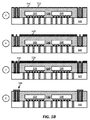
図10Aの段階1において示すように、基板1002を設ける(たとえば、製作する)。いくつかの実装形態では、基板1002はウエハである。各実装形態では、基板用にそれぞれに異なる様々な材料を使用してもよい(たとえば、シリコン基板、ガラス基板、セラミック基板、有機基板)。基板1002は、基板貫通ビア(TSV)のセット1004とパッドのセット1005とを含む。いくつかの実装形態では、基板1002は他の配線(たとえば、トレース)を含んでもよい。パッドのセット1005は、基板1002の第1の表面(たとえば、上面)に埋め込まれる。いくつかの実装形態では、パッドのセット1005は基板1002の第1の表面(たとえば、上面)上に配置される。いくつかの実装形態では、基板1002の第1の表面上に誘電体層1003が結合される(たとえば、形成される)。いくつかの実装形態では、誘電体層1003は、絶縁層304と同様でありならびに/あるいは同じである。誘電体層1003は、1つまたは複数のパッド1005および/またはTSVの1つまたは複数のセット1004の上方に1つまたは複数の開口部および/またはキャビティを含んでもよい。いくつかの実装形態では、基板1002は、図を明確にするために示されていない配線(たとえば、トレース、ビア)のセットを含んでもよい。配線のセットは、1つまたは複数のパッド(たとえば、パッド1005)に結合されてもよい。
As shown in
段階2において、基板1002に第1のダイ1006および第2のダイ1008を結合する。第1のダイ1006を配線の第1のセット1016(たとえば、第1のピラー、第1のはんだ)を通して基板1002に結合する。いくつかの実装形態では、配線の第1のセットのうちの少なくとも1つの配線がTSVのセット1004のうちの少なくとも1つのTSVに電気的に結合される。第2のダイ1008は、配線の第2のセット1018(たとえば、第1のピラー、第1のはんだ)を通して基板1002に結合される。いくつかの実装形態では、配線の第2のセット1018のうちの少なくとも1つの配線をTSVのセット1004のうちの少なくとも1つのTSVに電気的に結合する。
In
段階3において、基板1002上および/または基板1002上の誘電体層1003上に封止層1020を設ける(たとえば、形成する)。封止層1020は、第1のダイ1006および第2のダイ1008を封止する。いくつかの実装形態では、封止層1020は基板1002に直接結合されてもよい。各実装形態は、封止層1020用にそれぞれに異なる材料を使用してもよい。いくつかの実装形態では、封止層1020は充填材ム層である。いくつかの実装形態では、封止層1020は、光パターニング可能特性を有する材料で作られる。
In
段階4において、封止層1020内に少なくとも1つのキャビティ1025を形成する。いくつかの実装形態では、キャビティ1025はパッド(たとえば、パッド1005)の上方に形成される(たとえば、作製される)。いくつかの実装形態では、キャビティ1025は、フォトエッチングプロセス(たとえば、フォトリソグラフィプロセス)を使用することによって形成される。
In
段階5において、バリア層1030を設ける(たとえば、形成する、堆積させる)。いくつかの実装形態では、バリア層1030を形成するためにめっきプロセスが使用される。バリア層1030は、キャビティ1025の内壁、パッド1005の少なくとも一部、および/または封止層1020の第1の表面を覆ってもよい。各実装形態は、バリア層1030用にそれぞれに異なる材料を使用してもよい。いくつかの実装形態では、バリア層1030は、少なくともチタン(Ti)、(TiN)、アルミニウム銅(AlCu)、チタン銅合金(TiCu)、および/またはチタンタングステン銅合金(TiWCu)のうちの1つである。しかしながら、各実装形態は、それぞれに異なる材料を使用してもよい。したがって、バリア層1030用の材料を上記に記載した材料に限定すべきではない。
In
バリア層1030上にシード層1032も設ける(たとえば、形成する、堆積させる)。いくつかの実装形態では、バリア層1030上にシード層1032を形成するためにめっきプロセスが使用される。各実装形態は、シード層1032用にそれぞれに異なる材料を使用してもよい。いくつかの実装形態では、シード層1032は金属層である。
A
段階6において、シード層1032上にフォトレジスト層1034を設ける(たとえば、形成する、堆積させる)。いくつかの実装形態では、フォトレジスト層1034を設けることは、フォトレジスト層1034を設けることと、フォトレジスト層1034のいくつかの部分を選択的に除去することとを含む。
In
段階7において、シード層1032上に金属層1036を設ける(たとえば、形成する、堆積させる)。いくつかの実装形態では、金属層1036は、フォトレジスト層1034によって覆われていないシード層1032上に設けられる。いくつかの実装形態では、シード層1032上に金属層1036を設けるためにリソグラフィおよびめっきプロセスが使用される。いくつかの実装形態では、金属層1036とシード層1032は同じ材料である。したがって、いくつかの実装形態では、金属層1036はシード層1032を含んでもよい。段階7に示すように、金属層1036は、バリア層1030に整合する(たとえば、バリア層1030の輪郭を形成する)ようにシード層1032上に設けられる。段階7は、金属層1036がキャビティ1025を完全には充填せず、キャビティ1037を残すことも示す。
In
段階8において、キャビティ1037内に充填材1039を設ける。各実装形態では、充填材1039用にそれぞれに異なる材料を使用してもよい。たとえば、充填材1039はポリマー充填材を含んでもよい。いくつかの実装形態では、充填材1039はビア構造の構造安定性を実現するように構成される。
In
段階9において、フォトレジスト層1034、シード層1032、およびバリア層1030を選択的に除去する(たとえば、エッチングする)。いくつかの実装形態では、フォトレジスト層1034、シード層1032、およびバリア層1030を同時に除去する。いくつかの実装形態では、フォトレジスト層1034、シード層1032、およびバリア層1030を順次除去する。段階9に示すように、フォトレジスト層1034、シード層1032、およびバリア層1030を選択的に除去した後にビア構造1038を製作する。いくつかの実装形態では、ビア構造1038は、図8および図9に記載されたビア構造のうちの1つである。
In step 9, the
段階10において、場合によっては、封止層1020の第2の表面上に誘電体層1040を設ける(たとえば、形成する)。いくつかの実装形態では、誘電体層1040の表面をビア構造1038の表面と揃える。いくつかの実装形態では、誘電体層1040はビア構造1038を覆ってもよく、ビア構造1038の一部の上方にキャビティを形成してもよい。
In
段階11において、場合によっては、基板1002の第2の表面(たとえば、底面)上に別の誘電体層1050を設ける(たとえば、形成する)。さらに、誘電体層1050上/内に配線のセット1052も設ける。いくつかの実装形態では、配線のセット1052は、再分配層および/またはアンダーバンプメタライゼーション(UBM)層の少なくとも一方を含む。いくつかの実装形態では、配線のセット1052のうちの少なくとも1つの配線をTSVのセット1004のうちの少なくとも1つのTSVに電気的に結合する。
In
段階12において、配線のセット1052にはんだボールのセット1054を結合する。いくつかの実装形態では、段階10の後、封止層と、サイドバリア層を含むビア構造とを含む集積デバイス1060を製作する。
In
封止層を横切るサイドバリア層と充填材とを有するビアを含む例示的な集積デバイス
図11は、ビア構造のセット1110を含む集積パッケージデバイスを示す。詳細には、図11は、ビア構造のセット1110を含むインターポーザ1100の一例を示す。いくつかの実装形態では、ビア構造1110は、図8に示すビア構造および/または本開示において説明し図示する任意の新規のビア構造であってもよい。
Exemplary Integrated Device Comprising Vias with Side Barrier Layers and Fillers Across the Sealing Layer FIG. 11 shows an integrated package device that includes a set of via
図11に示すように、インターポーザ1100は、封止層1102と、第1の誘電体層1104と、基板1106と、第1のパッド1108と、ビア構造のセット1110とを含む。第1の誘電体層1104は、封止層1102の第1の表面(たとえば、上面)に結合される。基板1106は、封止層1102の第2の表面(たとえば、底面)に結合される。いくつかの実装形態では、基板1106と封止層1102の第2の表面との間に第2の誘電体層(たとえば、封止層304)を位置させてもよい。
As shown in FIG. 11, the
ビア構造のセット1110は、封止層1102を横切る。いくつかの実装形態では、ビア構造のセット1110は少なくとも第1のパッド1108に結合される。ビア構造1110のうちの1つは、少なくともバリア層1112と、封止貫通ビア(TEV)1114と、充填材1116とを含む。バリア層1112、TEV 1114、および充填材1116は、封止層1102内に配置される。いくつかの実装形態では、バリア層1112はパッド1108に結合される(たとえば、直接接触する)。TEV 1114は、封止層1102を横切る金属層(たとえば、銅)である。いくつかの実装形態では、TEV 1114はシード層を含む。そのような場合、TEV 1114は金属層(たとえば、銅層)とシード層とを含む。いくつかの実装形態では、シード層は、TEV 1114の金属層とバリア層1112との間に位置する。TEV 1114は、第1の側面(たとえば、下側面)と、第2の側面(たとえば、上側面)と、第3の側面(たとえば、垂直側面)とを有する。いくつかの実装形態では、TEV 1114の第3の側面はTEV 1114の壁であってもよい。いくつかの実装形態では、TEV 1114は非水平側面を有してもよい。たとえば、TEV 1114は、非垂直側面または非水平側面(たとえば、対角側面)を有してもよい。各実装形態では、充填材1116にそれぞれに異なる材料を使用してもよい。たとえば、充填材1116はポリマー充填材を含んでもよい。いくつかの実装形態では、充填材1116はビア構造の構造安定性を実現する。
A set of via
図11は、TEV 1114がバリア層1112の形状に整合することを示す。この例では、バリア層1112はU字形断面を有する。同様に、TEV 1114はU字形断面を有する。図11は、充填材1116がTEV 1114に結合されることも示す。特に、充填材1116はTEV 1114に囲まれる。第1のバリア層1112は、TEV 1114に結合される。特に、TEV 1114は封止層1102内で第1のバリア層1112に囲まれる。第1のバリア層1112は、TEV 1114の第1の側面およびTEV 1114の第3の側面(たとえば、垂直側面)に結合される。したがって、図11に示すように、いくつかの実装形態では、TEV 1114が封止層1102に直接接触することはない(たとえば、直接的な接点を有さない)。各実装形態は、第1のバリア層1112用にそれぞれに異なる材料を使用してもよい。いくつかの実装形態では、第1のバリア層1112は、少なくともチタン(Ti)、TiN、および/またはTiWのうちの1つである。しかし、第1のバリア層1112は、他の材料であってもよく、列挙された材料に限定されない。
FIG. 11 shows that the
封止層を横切るサイドバリア層と充填材とを有するビアを含む集積デバイスを提供/製作する例示的なシーケンス
いくつかの実装形態では、集積デバイスはインターポーザを含んでもよい。いくつかの実装形態では、ビア構造を含む集積デバイス(たとえば、集積パッケージ)を提供することは、いくつかのプロセスを含む。図12(図12A〜図12Cを含む)は、集積デバイスを提供するための例示的なシーケンスを示す。いくつかの実装形態では、図12A〜図12Cのシーケンスは、図8、図9、および/または図11の集積デバイス、ならびに/あるいは本開示において説明する他の集積デバイスを提供する/製造するために使用されてもよい。
Exemplary Sequence for Providing / Manufacturing an Integrated Device Comprising Vias with Side Barrier Layers and Fillers Across the Sealing Layer In some implementations, the integrated device may include an interposer. In some implementations, providing an integrated device (eg, an integrated package) that includes a via structure includes a number of processes. FIG. 12 (including FIGS. 12A-12C) illustrates an exemplary sequence for providing an integrated device. In some implementations, the sequence of FIGS. 12A-12C provides / manufactures the integrated device of FIGS. 8, 9, and / or 11 and / or other integrated devices described in this disclosure. May be used.
図12A〜図12Cのシーケンスが、集積デバイスを提供するためのシーケンスを簡略化しならびに/あるいは明確化するために1つまたは複数の段階を組み合わせてもよいことにさらに留意されたい。 It is further noted that the sequence of FIGS. 12A-12C may combine one or more stages to simplify and / or clarify the sequence for providing an integrated device.
いくつかの実装形態では、図12A〜図12Cのプロセスは、高密度配線を有する集積デバイス(たとえば、インターポーザ)を提供する新規のプロセスを示す。 In some implementations, the processes of FIGS. 12A-12C illustrate a novel process for providing an integrated device (eg, an interposer) with high density wiring.
図12Aの段階1において示すように、キャリア1202を設ける(たとえば、製作する)。いくつかの実装形態では、キャリア1202は、少なくとも基板および/またはウエハの一方である。各実装形態では、キャリア用にそれぞれに異なる様々な材料を使用してもよい(たとえば、シリコン基板、ガラス基板、セラミック基板、有機基板)。キャリア1202は、パッドのセット1205を含む。いくつかの実装形態では、キャリア1202は他の配線(たとえば、トレース)を含んでもよい。パッドのセット1205はキャリア1202の第1の表面(たとえば、上面)に埋め込まれる。いくつかの実装形態では、パッドのセット1205はキャリア1202の第1の表面(たとえば、上面)上に配置される。いくつかの実装形態では、基板1204の第1の表面上に誘電体層1203が結合される(たとえば、形成される)。いくつかの実装形態では、誘電体層は、絶縁層304と同様でありならびに/あるいは同じである。
As shown in
段階2において、キャリア1202上および/またはキャリア1202上の誘電体層1203上に封止層1220を設ける(たとえば、形成する)。いくつかの実装形態では、封止層1220はパッド1205を封止する。いくつかの実装形態では、封止層1220はキャリア1202に直接結合されてもよい。各実装形態は、封止層1220用にそれぞれに異なる材料を使用してもよい。いくつかの実装形態では、封止層1220は充填材ム層である。いくつかの実装形態では、封止層1220は、光パターニング可能特性を有する材料で作られる。いくつかの実装形態では、封止層1220は、フォトエッチングプロセスによって除去する(たとえば、エッチングする)ことができる材料で作られる。
In
段階3において、封止層1220内に少なくとも1つのキャビティ1225を形成する。いくつかの実装形態では、キャビティ1225はパッド(たとえば、パッド1205)の上方に形成される(たとえば、作製される)。いくつかの実装形態では、キャビティ1225は、フォトエッチングプロセス(たとえば、フォトリソグラフィプロセス)を使用することによって形成される。
In
段階4において、バリア層1230を設ける(たとえば、形成する、堆積させる)。いくつかの実装形態では、バリア層1230を形成するためにめっきプロセスが使用される。バリア層1230は、キャビティ1225の内壁、パッド1205の少なくとも一部、および/または封止層1220の第1の表面を覆ってもよい。各実装形態は、バリア層1230用にそれぞれに異なる材料を使用してもよい。各実装形態は、バリア層1230用にそれぞれに異なる材料を使用してもよい。いくつかの実装形態では、バリア層1230は、少なくともチタン(Ti)、(TiN)、アルミニウム銅(AlCu)、チタン銅合金(TiCu)、および/またはチタンタングステン銅合金(TiWCu)のうちの1つである。
In
バリア層1230上にシード層1232も設ける(たとえば、形成する、堆積させる)。いくつかの実装形態では、バリア層1230上にシード層1232を形成するためにめっきプロセスが使用される。各実装形態は、シード層1232用にそれぞれに異なる材料を使用してもよい。いくつかの実装形態では、シード層1232は金属層である。
A
段階5において、シード層1232上にフォトレジスト層1234を設ける(たとえば、形成する、堆積させる)。いくつかの実装形態では、フォトレジスト層1234を設けることは、フォトレジスト層1234を設けることと、フォトレジスト層1234のいくつかの部分を選択的に除去することとを含む。
In
段階6において、シード層1232上に金属層1236を設ける(たとえば、形成する、堆積させる)。いくつかの実装形態では、金属層1236は、フォトレジスト層1234によって覆われていないシード層1232上に設けられる。いくつかの実装形態では、シード層1232上に金属層1236を設けるためにリソグラフィおよびめっきプロセスが使用される。いくつかの実装形態では、金属層1236とシード層1232は同じ材料である。したがって、いくつかの実装形態では、金属層1236はシード層1232を含んでもよい。
In
段階6に示すように、金属層1236は、バリア層1230に整合する(たとえば、バリア層1230の輪郭を形成する)ようにシード層1232上に設けられる。段階6は、金属層1236がキャビティ1225を完全には充填せず、キャビティ1237を残すことも示す。
As shown in
段階7において、キャビティ1237内に充填材1239を設ける。各実装形態では、充填材1239用にそれぞれに異なる材料を使用してもよい。たとえば、充填材1239はポリマー充填材を含んでもよい。いくつかの実装形態では、充填材1239はビア構造の構造安定性を実現するように構成される。
In
段階8において、フォトレジスト層1234、シード層1232、およびバリア層1230を選択的に除去する(たとえば、エッチングする)。いくつかの実装形態では、フォトレジスト層1234、シード層1232、およびバリア層1230を同時に除去するか、あるいはフォトレジスト層1234、シード層1232、およびバリア層1230を順次除去する。段階12に示すように、フォトレジスト層1234、シード層1232、およびバリア層1230を選択的に除去した後にビア構造1238を製作する。いくつかの実装形態では、ビア構造1238は、図8および図9に記載されたビア構造のうちの1つである。
In
段階9において、場合によっては、封止層1220の第2の表面上に誘電体層1240を設ける(たとえば、形成する)。いくつかの実装形態では、誘電体層1240の表面をビア構造1238の表面と揃える。いくつかの実装形態では、誘電体層1240はビア構造1238を覆ってもよく、ビア構造1238の一部の上方にキャビティを形成してもよい。
In step 9, a
段階10において、キャリア1202の少なくとも一部を除去する(たとえば、研磨する、研削する、エッチングする)。いくつかの実装形態では、キャリア1202は、キャリア1202の表面がパッド1205の表面と揃えられるまで除去される。いくつかの実装形態では、段階10の後、封止層と、サイドバリア層を含むビア構造とを含む集積デバイス1260を製作する。
In
封止層を横切るサイドバリア層を有するビアを含む集積デバイスを提供/製作する例示的な方法
いくつかの実装形態では、ビア構造を含む集積デバイス(たとえば、集積パッケージ)を提供することは、いくつかのプロセスを含む。図13は、集積デバイスを提供する方法を示す。いくつかの実装形態では、図13の方法は、図3、図4、図8、および/または図9の集積デバイス、ならびに/あるいは本開示において説明する他の集積デバイスを提供する/製造するために使用されてもよい。
Exemplary Method of Providing / Manufacturing an Integrated Device Comprising a Via With a Side Barrier Layer Across a Sealing Layer In some implementations, providing an integrated device (eg, an integrated package) that includes a via structure is Process. FIG. 13 illustrates a method for providing an integrated device. In some implementations, the method of FIG. 13 provides / manufactures the integrated device of FIGS. 3, 4, 8, and / or 9 and / or other integrated devices described in this disclosure. May be used.
図13の方法が、回路要素も含む集積デバイスを提供する/製造するために使用されてもよいことにも留意されたい。図13の方法が、集積デバイスを提供するためのシーケンスを簡略化しならびに/あるいは明確化するために1つまたは複数の段階を組み合わせてもよいことにさらに留意されたい。 It should also be noted that the method of FIG. 13 may be used to provide / manufacture an integrated device that also includes circuit elements. It is further noted that the method of FIG. 13 may combine one or more stages to simplify and / or clarify the sequence for providing an integrated device.
いくつかの実装形態では、図13のプロセスは、高密度配線を有する集積デバイスを提供する新規のプロセスを示す。 In some implementations, the process of FIG. 13 illustrates a novel process for providing an integrated device with high density wiring.
この方法では、(1305において)基板を設ける。いくつかの実装形態では、基板を設けることは、基板(たとえば、基板502)を形成しならびに/あるいは製作することを含んでもよい。いくつかの実装形態では、基板はウエハである。各実装形態では、基板用にそれぞれに異なる様々な材料を使用してもよい(たとえば、シリコン基板、ガラス基板、セラミック基板、有機基板)。基板は、基板貫通ビア(TSV)のセットとパッドのセットとを含んでもよい。いくつかの実装形態では、基板は他の配線(たとえば、トレース)を含んでもよい。いくつかの実装形態では、パッドのセットは基板の第1の表面(たとえば、上面)上に配置される。いくつかの実装形態では、パッドのセットは、基板の第1の表面に埋め込まれる。いくつかの実装形態では、基板は、基板の第1の表面上に結合される(たとえば、形成される)誘電体層を含んでもよい。 In this method, a substrate is provided (at 1305). In some implementations, providing a substrate may include forming and / or fabricating a substrate (eg, substrate 502). In some implementations, the substrate is a wafer. In each mounting form, various different materials may be used for the substrate (for example, silicon substrate, glass substrate, ceramic substrate, organic substrate). The substrate may include a set of through-substrate vias (TSVs) and a set of pads. In some implementations, the substrate may include other wiring (eg, traces). In some implementations, the set of pads is disposed on the first surface (eg, the top surface) of the substrate. In some implementations, the set of pads is embedded in the first surface of the substrate. In some implementations, the substrate may include a dielectric layer that is bonded (eg, formed) on the first surface of the substrate.
その方法ではさらに、(1310において)基板に少なくとも1つのダイを設ける。いくつかの実装形態では、少なくとも1つのダイを設けることは、第1のダイおよび第2のダイを基板に結合することを含む。いくつかの実装形態では、第1のダイが配線の第1のセット(たとえば、第1のピラー、第1のはんだ)を通して基板に結合される。 The method further provides (at 1310) at least one die on the substrate. In some implementations, providing at least one die includes coupling the first die and the second die to the substrate. In some implementations, the first die is coupled to the substrate through a first set of wiring (eg, first pillar, first solder).
この方法では、(1315において)封止層も設ける。いくつかの実装形態では、封止層を設けることは、基板上および/または基板上の誘電体層上に封止層を形成することを含む。いくつかの実装形態では、封止層は第1のダイを封止する。各実装形態は、封止層用にそれぞれに異なる材料を使用してもよい。いくつかの実装形態では、封止層は充填材ム層である。いくつかの実装形態では、封止層は、光パターニング可能特性を有する材料で作られる。 In this method, a sealing layer is also provided (at 1315). In some implementations, providing the sealing layer includes forming the sealing layer on the substrate and / or on the dielectric layer on the substrate. In some implementations, the sealing layer seals the first die. Each mounting form may use a different material for the sealing layer. In some implementations, the sealing layer is a filler layer. In some implementations, the encapsulation layer is made of a material that has photopatternable properties.
この方法では次に、(1320において)封止層にバリア層を含む少なくとも1つのビアを設ける。いくつかの実装形態では、バリア層を含む少なくとも1つのビアを設けることは、封止層内にキャビティを形成することと、キャビティ内に少なくとも1つの金属層を設けることとを含む。いくつかの実装形態では、キャビティはパッドの上方に形成される(たとえば、作製される)。いくつかの実装形態では、キャビティは、フォトエッチングプロセス(たとえば、フォトリソグラフィプロセス)を使用することによって形成される。 The method then provides (at 1320) at least one via that includes a barrier layer in the encapsulation layer. In some implementations, providing at least one via that includes a barrier layer includes forming a cavity in the encapsulation layer and providing at least one metal layer in the cavity. In some implementations, the cavity is formed (eg, made) above the pad. In some implementations, the cavities are formed by using a photoetching process (eg, a photolithography process).
いくつかの実装形態では、少なくとも1つの金属層を設けることは、キャビティ内にバリア層を設ける(たとえば、形成する)ことを含む。いくつかの実装形態では、バリア層を形成するためにめっきプロセスが使用される。バリア層は、キャビティの内壁、パッドの少なくとも一部、および/または封止層の第1の表面を覆ってもよい。各実装形態は、バリア層用にそれぞれに異なる材料を使用してもよい。いくつかの実装形態では、バリア層は、少なくともチタン(Ti)、(TiN)、アルミニウム銅(AlCu)、チタン銅合金(TiCu)、および/またはチタンタングステン銅合金(TiWCu)のうちの1つである。しかしながら、各実装形態は、それぞれに異なる材料を使用してもよい。したがって、バリア層用の材料を上記に記載した材料に限定すべきではない。 In some implementations, providing at least one metal layer includes providing (eg, forming) a barrier layer within the cavity. In some implementations, a plating process is used to form the barrier layer. The barrier layer may cover the inner wall of the cavity, at least a portion of the pad, and / or the first surface of the sealing layer. Each implementation may use a different material for the barrier layer. In some implementations, the barrier layer is at least one of titanium (Ti), (TiN), aluminum copper (AlCu), titanium copper alloy (TiCu), and / or titanium tungsten copper alloy (TiWCu). is there. However, each implementation may use a different material. Therefore, the material for the barrier layer should not be limited to the materials described above.
いくつかの実装形態では、少なくとも1つの金属層を設けることは、バリア層上にシード層を設ける(たとえば、形成する、堆積させる)ことをさらに含む。いくつかの実装形態では、バリア層上にシード層を形成するためにめっきプロセスが使用される。各実装形態は、シード層用にそれぞれに異なる材料を使用してもよい。 In some implementations, providing the at least one metal layer further includes providing (eg, forming, depositing) a seed layer over the barrier layer. In some implementations, a plating process is used to form a seed layer on the barrier layer. Each implementation may use a different material for the seed layer.
いくつかの実装形態では、バリア層を有するビアを設けることは、シード層上にフォトレジスト層を設ける(たとえば、形成する、堆積させる)ことをさらに含む。いくつかの実装形態では、フォトレジスト層を設けることは、フォトレジスト層534を設けることと、フォトレジスト層のいくつかの部分を選択的に除去することとを含む。
In some implementations, providing the via with the barrier layer further includes providing (eg, forming, depositing) a photoresist layer over the seed layer. In some implementations, providing the photoresist layer includes providing a
この方法では次いで、シード層上に金属層を設ける。いくつかの実装形態では、金属層は、フォトレジスト層によって覆われていないシード層上に設けられる。いくつかの実装形態では、シード層上に金属層を設けるためにリソグラフィおよびめっきプロセスが使用される。いくつかの実装形態では、金属層とシード層は同じ材料である。したがって、いくつかの実装形態では、金属層はシード層を含んでもよい。 The method then provides a metal layer on the seed layer. In some implementations, the metal layer is provided on a seed layer that is not covered by a photoresist layer. In some implementations, lithography and plating processes are used to provide a metal layer on the seed layer. In some implementations, the metal layer and the seed layer are the same material. Thus, in some implementations, the metal layer may include a seed layer.
この方法では次いで、フォトレジスト層、シード層、およびバリア層を選択的に除去する(たとえば、エッチングする)。いくつかの実装形態では、フォトレジスト層、シード層、およびバリア層を同時に除去する。いくつかの実装形態では、フォトレジスト層、シード層、およびバリア層を順次除去する。 The method then selectively removes (eg, etches) the photoresist layer, seed layer, and barrier layer. In some implementations, the photoresist layer, seed layer, and barrier layer are removed simultaneously. In some implementations, the photoresist layer, seed layer, and barrier layer are removed sequentially.
いくつかの実装形態では、場合によっては、封止層の第2の表面上に誘電体層を設けてもよい(たとえば、形成してもよい)。いくつかの実装形態では、場合によっては、基板の第2の表面(たとえば、底面)上に別の誘電体層を設けてもよい(たとえば、形成してもよい)。さらに、誘電体層上/内に配線のセットを設けてもよい。 In some implementations, in some cases, a dielectric layer may be provided (eg, formed) on the second surface of the encapsulation layer. In some implementations, in some cases, another dielectric layer may be provided (eg, formed) on the second surface (eg, the bottom surface) of the substrate. Furthermore, a set of wirings may be provided on / in the dielectric layer.
例示的な電子デバイス
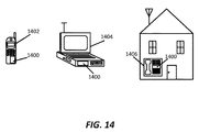
図14は、上述の集積デバイス、半導体デバイス、集積回路、ダイ、インターポーザ、またはパッケージのうちのいずれかと一体化される場合がある様々な電子デバイスを示す。たとえば、モバイル電話1402、ラップトップコンピュータ1404、および固定位置端末1406が、本明細書で説明する集積デバイス1400を含んでもよい。集積デバイス1400は、たとえば、本明細書で説明する集積回路、ダイ、インターポーザ、またはパッケージのうちのいずれかであってもよい。図14に示すデバイス1402、1404、1406は例にすぎない。他の電子デバイスは、限定はされないが、モバイルデバイス、ハンドヘルドパーソナル通信システム(PCS,personal communication system)ユニット、携帯情報端末などのポータブルデータユニット、GPS対応デバイス、ナビゲーションデバイス、セットトップボックス、音楽プレーヤ、ビデオプレーヤ、エンターテイメントユニット、メータ読取り機器などの固定位置データユニット、通信デバイス、スマートフォン、タブレットコンピュータ、またはデータもしくはコンピュータ命令を記憶し、もしくは取り出す任意の他のデバイス、またはそれらの任意の組合せを含む、集積デバイス1400を特徴としてもよい。
Exemplary Electronic Device FIG. 14 illustrates various electronic devices that may be integrated with any of the integrated devices, semiconductor devices, integrated circuits, dies, interposers, or packages described above. For example,
図3、図4、図5A〜図5C、図6、図7A〜図7C、図8、図9、図10A〜図10C、図11、図12A〜図12C、図13、および/または図14に示した構成要素、ステップ、特徴、および/または機能のうちの1つまたは複数は、単一の構成要素、ステップ、特徴または機能に再構成され、かつ/または組み合わされ、あるいは、いくつかの構成要素、ステップ、または機能で具現化され得る。追加の要素、構成要素、ステップ、および/または機能を、本開示から逸脱せずに追加してもよい。本開示における図3、図4、図5A〜図5C、図6、図7A〜図7C、図8、図9、図10A〜図10C、図11、図12A〜図12C、図13、および/または図14と、その対応する説明とは、ダイおよび/またはICに限定されないことにも留意されたい。いくつかの実装形態では、図3、図4、図5A〜図5C、図6、図7A〜図7C、図8、図9、図10A〜図10C、図11、図12A〜図12C、図13、および/または図14と、その対応する説明とは、集積デバイスを製造し、作製し、提供し、かつ/または生産するために使用され得る。いくつかの実装形態では、集積デバイスは、ダイパッケージ、集積回路(IC,integrated circuit)、ウエハ、半導体デバイス、および/またはインターポーザを含んでもよい。 3, 4, 5A-5C, 6, 7A-7C, 8, 9, 10A-10C, 11, 12A-12C, 13, and / or 14 One or more of the components, steps, features, and / or functions shown in FIG. 5 may be reconfigured and / or combined into a single component, step, feature, or function, or It may be implemented with components, steps, or functions. Additional elements, components, steps, and / or functions may be added without departing from the present disclosure. 3, 4, 5A-5C, 6, 7A-7C, 8, 9, 10A-10C, 11, 12, 12A-12C, 13, and / or in this disclosure It should also be noted that FIG. 14 and its corresponding description are not limited to dies and / or ICs. In some implementations, FIGS. 3, 4, 5A-5C, 6, 7A-7C, 8, 9, 10A-10C, 11, 12A-12C, FIG. 13, and / or FIG. 14 and its corresponding description can be used to manufacture, fabricate, provide, and / or produce integrated devices. In some implementations, the integrated device may include a die package, an integrated circuit (IC), a wafer, a semiconductor device, and / or an interposer.
「例示的」という言葉は、「例、事例、または例示として働く」ことを意味するように本明細書において使用される。「例示的」として本明細書で説明した任意の実装形態または態様は、必ずしも本開示の他の態様よりも好ましいかまたは有利であると解釈されるべきではない。同様に、「態様」という用語は、本開示のすべての態様が記載の特徴、利点、または動作モードを含むことを必要としない。「結合された」という用語は、本明細書において、2つの物体間の直接的または間接的な結合を指すために使用される。たとえば、物体Aが物体Bに物理的に接触し、物体Bが物体Cに接触する場合、物体Aと物体Cとは、互いに物理的に直接接触していなくても、それでも互いに結合するものと見なされてもよい。 The word “exemplary” is used herein to mean “serving as an example, instance, or illustration”. Any implementation or aspect described herein as "exemplary" is not necessarily to be construed as preferred or advantageous over other aspects of the disclosure. Similarly, the term “aspect” does not require that all aspects of the disclosure include the described features, advantages, or modes of operation. The term “coupled” is used herein to refer to a direct or indirect coupling between two objects. For example, when object A physically touches object B and object B touches object C, object A and object C are still in direct contact with each other even if they are not in direct physical contact with each other. May be considered.
また、実施形態については、フローチャート、流れ図、構造図、またはブロック図として示されるプロセスとして説明する場合があることに留意されたい。フローチャートでは動作を逐次プロセスとして説明する場合があるが、動作の多くは、並列に実行するかまたは同時に実行することができる。さらに、動作の順序は入れ替えられてもよい。プロセスは、その動作が完了したとき、終了する。 It should also be noted that the embodiments may be described as a process which is depicted as a flowchart, a flow diagram, a structure diagram, or a block diagram. Although a flowchart may describe the operations as a sequential process, many of the operations can be performed in parallel or concurrently. Furthermore, the order of operations may be switched. The process ends when its operation is complete.
本明細書で説明する本開示の様々な特徴は、本開示から逸脱することなく様々なシステムにおいて実現されてもよい。本開示の前述の態様は、例にすぎず、本開示を限定するものとして解釈されるべきではないことに留意されたい。本開示の態様の説明は、例示であることを意図しており、特許請求の範囲を限定することを意図していない。したがって、本教示は、他のタイプの装置に容易に適用することができ、数多くの代替、修正、および変形が、当業者には明らかになるであろう。 Various features of the present disclosure described herein may be implemented in various systems without departing from the disclosure. It should be noted that the foregoing aspects of the disclosure are examples only and should not be construed as limiting the disclosure. The descriptions of aspects of the disclosure are intended to be illustrative and are not intended to limit the scope of the claims. Accordingly, the present teachings can be readily applied to other types of devices and numerous alternatives, modifications, and variations will be apparent to those skilled in the art.
102 第1のパッケージ
104 第2のパッケージ
105 第2の基板
106 第1の基板
107 第2のダイ
108 第1のダイ
109 第3のダイ
110 モールド
115 はんだボールの第2のセット
116 はんだボールの第1のセット
117 ワイヤボンディングの第1のセット
118 配線の第1のセット
119 ワイヤボンディングの第2のセット
126 はんだボールの第3のセット
200 集積デバイス
302 基板
304 絶縁層
306 封止層
308 誘電体層
310 第1のパッド
312 第1のバリア層
314 封止貫通ビア(TEV)
315 キャビティ
400 集積パッケージデバイス
401 ビア構造
402 基板
403 第1のバリア層
404 第1のダイ
405 封止貫通ビア(TEV)
406 第2のダイ
409 誘電体層
414 配線の第1のセット
416 配線の第2のセット
418 封止層
420 第1の誘電体層
422 第2の誘電体層
426 配線の第3のセット
428 はんだボールのセット
430 第1のパッド
502 基板
503 誘電体層
504 基板貫通ビア(TSV)のセット
505 パッドのセット
506 第1のダイ
508 第2のダイ
516 配線の第1のセット
518 配線の第2のセット
520 封止層
525 キャビティ
530 バリア層
532 シード層
534 フォトレジスト層
536 金属層
538 ビア構造
540 誘電体層
550 誘電体層
552 配線のセット
554 はんだボールのセット
560 集積デバイス
600 インターポーザ
602 封止層
604 第1の誘電体層
606 基板
608 第1のパッド
610 ビア構造のセット
612 バリア層
614 封止貫通ビア(TEV)
702 キャリア
703 誘電体層
704 基板
705 パッドのセット
720 封止層
725 キャビティ
730 バリア層
732 シード層
734 フォトレジスト層
736 金属層
738 ビア構造
740 誘電体層
760 集積デバイス
802 基板
804 絶縁層
806 封止層
808 誘電体層
810 第1のパッド
812 第1のバリア層
814 封止貫通ビア(TEV)
816 充填材
817 キャビティ
900 集積パッケージデバイス
901 ビア構造のセット
902 基板
903 第1のバリア層
904 第1のダイ
905 封止貫通ビア(TEV)
906 第2のダイ
907 充填材
909 誘電体層
914 配線の第1のセット
916 配線の第2のセット
918 封止層
920 第1の誘電体層
922 第2の誘電体層
924 基板貫通ビア(TSV)のセット
926 配線の第3のセット
928 はんだボールのセット
930 第1のパッド
1002 基板
1003 誘電体層
1004 基板貫通ビア(TSV)のセット
1005 パッドのセット
1006 第1のダイ
1008 第2のダイ
1016 配線の第1のセット
1018 配線の第2のセット
1020 封止層
1025 キャビティ
1030 バリア層
1032 シード層
1034 フォトレジスト層
1036 金属層
1037 キャビティ
1038 ビア構造
1039 充填材
1040 誘電体層
1050 誘電体層
1052 配線のセット
1054 はんだボールのセット
1060 集積デバイス
1100 インターポーザ
1102 封止層
1104 第1の誘電体層
1106 基板
1108 第1のパッド
1110 ビア構造のセット
1112 第1のバリア層
1114 封止貫通ビア(TEV)
1116 充填材
1202 キャリア
1203 誘電体層
1204 基板
1205 パッドのセット
1220 封止層
1225 キャビティ
1230 バリア層
1232 シード層
1234 フォトレジスト層
1236 金属層
1237 キャビティ
1238 ビア構造
1239 充填材
1240 誘電体層
1260 集積デバイス
1400 集積デバイス
1402 モバイル電話
1404 ラップトップコンピュータ
1406 固定位置端末
102
315
406 Second die 409
702
816
906 Second die 907
1116
Claims (30)
前記封止層を横切るビア構造であって、
第1の側面と、第2の側面と、第3の側面とを備えるビアと、
前記ビアの少なくとも前記第1の側面と前記第3の側面を囲むバリア層とを備えるビア構造と、
前記ビア構造の前記バリア層に直接結合されたパッドとを備える集積デバイス。 A sealing layer;
A via structure across the sealing layer,
A via comprising a first side, a second side, and a third side;
A via structure comprising at least the first side surface of the via and a barrier layer surrounding the third side surface;
An integrated device comprising a pad directly coupled to the barrier layer of the via structure.
前記封止層を横切るビア構造であって、
第1の側面と、第2の側面と、第3の側面とを備えるビアと、
前記ビアの少なくとも前記第1の側面と前記第3の側面を囲むバリア手段とを備えるビア構造と、
前記ビア構造の前記バリア手段に直接結合されたパッドとを備える装置。 A sealing layer;
A via structure across the sealing layer,
A via comprising a first side, a second side, and a third side;
A via structure comprising barrier means surrounding at least the first side surface and the third side surface of the via;
And a pad directly coupled to the barrier means of the via structure.
基板上にパッドを形成するステップと、
前記基板上に封止層を形成するステップと、
前記封止層内にビア構造を形成するステップとを含み、前記ビア構造を形成する前記ステップは、
前記封止層内にバリア層を形成するステップと、
前記バリア層上にビアを形成するステップとを含み、前記ビアは、第1の側面と、第2の側面と、第3の側面とを備え、前記ビアは、前記バリア層が前記ビアの少なくとも前記第1の側面と前記第3の側面を囲むように前記バリア層上に形成され、前記バリア層はパッドに直接結合される、方法。 A method for fabricating an integrated device comprising:
Forming a pad on the substrate;
Forming a sealing layer on the substrate;
Forming a via structure in the sealing layer, and forming the via structure comprises the steps of:
Forming a barrier layer in the sealing layer;
Forming a via on the barrier layer, the via including a first side, a second side, and a third side, wherein the via has at least the barrier layer of the via. Forming on the barrier layer to surround the first side and the third side, and the barrier layer is directly bonded to a pad;
Applications Claiming Priority (5)
| Application Number | Priority Date | Filing Date | Title |
|---|---|---|---|
| US201461939523P | 2014-02-13 | 2014-02-13 | |
| US61/939,523 | 2014-02-13 | ||
| US14/274,517 US9466554B2 (en) | 2014-02-13 | 2014-05-09 | Integrated device comprising via with side barrier layer traversing encapsulation layer |
| US14/274,517 | 2014-05-09 | ||
| PCT/US2015/015421 WO2015123301A1 (en) | 2014-02-13 | 2015-02-11 | Integrated device comprising via with side barrier layer traversing encapsulation layer |
Publications (2)
| Publication Number | Publication Date |
|---|---|
| JP2017511971A true JP2017511971A (en) | 2017-04-27 |
| JP2017511971A5 JP2017511971A5 (en) | 2018-02-08 |
Family
ID=53775574
Family Applications (1)
| Application Number | Title | Priority Date | Filing Date |
|---|---|---|---|
| JP2016550191A Ceased JP2017511971A (en) | 2014-02-13 | 2015-02-11 | Integrated device comprising a via having a side barrier layer across the sealing layer |
Country Status (5)
| Country | Link |
|---|---|
| US (1) | US9466554B2 (en) |
| EP (1) | EP3105787B1 (en) |
| JP (1) | JP2017511971A (en) |
| CN (1) | CN105981166B (en) |
| WO (1) | WO2015123301A1 (en) |
Families Citing this family (5)
| Publication number | Priority date | Publication date | Assignee | Title |
|---|---|---|---|---|
| US9343417B2 (en) * | 2013-09-18 | 2016-05-17 | Taiwan Semiconductor Manufacturing Company, Ltd. | Hollow metal pillar packaging scheme |
| US9385110B2 (en) | 2014-06-18 | 2016-07-05 | Taiwan Semiconductor Manufacturing Company, Ltd. | Semiconductor device and method |
| US9355963B2 (en) * | 2014-09-26 | 2016-05-31 | Qualcomm Incorporated | Semiconductor package interconnections and method of making the same |
| TWI559829B (en) * | 2014-10-22 | 2016-11-21 | 矽品精密工業股份有限公司 | Package structure and method of fabricating the same |
| US10651160B2 (en) | 2017-03-20 | 2020-05-12 | Qualcomm Incorporated | Low profile integrated package |
Citations (7)
| Publication number | Priority date | Publication date | Assignee | Title |
|---|---|---|---|---|
| WO2010041630A1 (en) * | 2008-10-10 | 2010-04-15 | 日本電気株式会社 | Semiconductor device and method for manufacturing same |
| US20100155920A1 (en) * | 2008-12-24 | 2010-06-24 | Samsung Electronics Co., Ltd. | Stacked semiconductor package, semiconductor package module and method of manufacturing the stacked semiconductor package |
| JP2011238674A (en) * | 2010-05-07 | 2011-11-24 | Seiko Epson Corp | Wiring board, piezoelectric oscillator, gyro sensor, and method for manufacturing wiring board |
| JP2012119688A (en) * | 2010-12-02 | 2012-06-21 | Samsung Electronics Co Ltd | Stacked package structure, package-on-package element, and method of manufacturing package-on-package element |
| JP2012129262A (en) * | 2010-12-13 | 2012-07-05 | Sumitomo Bakelite Co Ltd | Manufacturing method of semiconductor element sealing body and manufacturing method of semiconductor package |
| US20120168944A1 (en) * | 2010-12-30 | 2012-07-05 | Stmicroelectronics Pte Ltd. | Through hole via filling using electroless plating |
| JP2013535834A (en) * | 2010-07-23 | 2013-09-12 | テッセラ,インコーポレイテッド | Microelectronic elements flattened after assembly |
Family Cites Families (12)
| Publication number | Priority date | Publication date | Assignee | Title |
|---|---|---|---|---|
| US6586682B2 (en) | 2000-02-23 | 2003-07-01 | Kulicke & Soffa Holdings, Inc. | Printed wiring board with controlled line impedance |
| GB0330010D0 (en) * | 2003-12-24 | 2004-01-28 | Cavendish Kinetics Ltd | Method for containing a device and a corresponding device |
| JP2005235860A (en) * | 2004-02-17 | 2005-09-02 | Sanyo Electric Co Ltd | Semiconductor device and manufacturing method thereof |
| US8239162B2 (en) * | 2006-04-13 | 2012-08-07 | Tanenhaus & Associates, Inc. | Miniaturized inertial measurement unit and associated methods |
| US8021981B2 (en) | 2006-08-30 | 2011-09-20 | Micron Technology, Inc. | Redistribution layers for microfeature workpieces, and associated systems and methods |
| DE102007020266B3 (en) * | 2007-04-30 | 2008-11-13 | Advanced Micro Devices, Inc., Sunnyvale | Semiconductor structure with an electrically conductive structural element and method for its preparation |
| JP5596919B2 (en) * | 2008-11-26 | 2014-09-24 | キヤノン株式会社 | Manufacturing method of semiconductor device |
| US7799602B2 (en) | 2008-12-10 | 2010-09-21 | Stats Chippac, Ltd. | Semiconductor device and method of forming a shielding layer over a semiconductor die after forming a build-up interconnect structure |
| JP2010157690A (en) | 2008-12-29 | 2010-07-15 | Ibiden Co Ltd | Board for mounting electronic component thereon, and method of manufacturing the same |
| US8476770B2 (en) * | 2011-07-07 | 2013-07-02 | Taiwan Semiconductor Manufacturing Company, Ltd. | Apparatus and methods for forming through vias |
| US9040346B2 (en) | 2012-05-03 | 2015-05-26 | Infineon Technologies Ag | Semiconductor package and methods of formation thereof |
| US8981559B2 (en) | 2012-06-25 | 2015-03-17 | Taiwan Semiconductor Manufacturing Company, Ltd. | Package on package devices and methods of packaging semiconductor dies |
-
2014
- 2014-05-09 US US14/274,517 patent/US9466554B2/en active Active
-
2015
- 2015-02-11 JP JP2016550191A patent/JP2017511971A/en not_active Ceased
- 2015-02-11 WO PCT/US2015/015421 patent/WO2015123301A1/en active Application Filing
- 2015-02-11 CN CN201580008236.2A patent/CN105981166B/en not_active Expired - Fee Related
- 2015-02-11 EP EP15706345.4A patent/EP3105787B1/en active Active
Patent Citations (7)
| Publication number | Priority date | Publication date | Assignee | Title |
|---|---|---|---|---|
| WO2010041630A1 (en) * | 2008-10-10 | 2010-04-15 | 日本電気株式会社 | Semiconductor device and method for manufacturing same |
| US20100155920A1 (en) * | 2008-12-24 | 2010-06-24 | Samsung Electronics Co., Ltd. | Stacked semiconductor package, semiconductor package module and method of manufacturing the stacked semiconductor package |
| JP2011238674A (en) * | 2010-05-07 | 2011-11-24 | Seiko Epson Corp | Wiring board, piezoelectric oscillator, gyro sensor, and method for manufacturing wiring board |
| JP2013535834A (en) * | 2010-07-23 | 2013-09-12 | テッセラ,インコーポレイテッド | Microelectronic elements flattened after assembly |
| JP2012119688A (en) * | 2010-12-02 | 2012-06-21 | Samsung Electronics Co Ltd | Stacked package structure, package-on-package element, and method of manufacturing package-on-package element |
| JP2012129262A (en) * | 2010-12-13 | 2012-07-05 | Sumitomo Bakelite Co Ltd | Manufacturing method of semiconductor element sealing body and manufacturing method of semiconductor package |
| US20120168944A1 (en) * | 2010-12-30 | 2012-07-05 | Stmicroelectronics Pte Ltd. | Through hole via filling using electroless plating |
Also Published As
| Publication number | Publication date |
|---|---|
| US20150228556A1 (en) | 2015-08-13 |
| US9466554B2 (en) | 2016-10-11 |
| CN105981166B (en) | 2019-04-16 |
| EP3105787B1 (en) | 2021-08-25 |
| WO2015123301A1 (en) | 2015-08-20 |
| EP3105787A1 (en) | 2016-12-21 |
| CN105981166A (en) | 2016-09-28 |
Similar Documents
| Publication | Publication Date | Title |
|---|---|---|
| TWI575693B (en) | Integrated device comprising high density interconnects in inorganic layers and redistribution layers in organic layers | |
| JP6309643B2 (en) | Integrated device with stacked die on redistribution layer | |
| JP6505951B2 (en) | Integrated device with embedded package on package (PoP) device | |
| TWI588965B (en) | Package-on-package device and methods of forming same | |
| US9947642B2 (en) | Package-on-Package (PoP) device comprising a gap controller between integrated circuit (IC) packages | |
| US9153560B2 (en) | Package on package (PoP) integrated device comprising a redistribution layer | |
| US9230936B2 (en) | Integrated device comprising high density interconnects and redistribution layers | |
| US9368566B2 (en) | Package on package (PoP) integrated device comprising a capacitor in a substrate | |
| US20160343646A1 (en) | High aspect ratio interconnect for wafer level package (wlp) and integrated circuit (ic) package | |
| JP2017511971A (en) | Integrated device comprising a via having a side barrier layer across the sealing layer | |
| US9355898B2 (en) | Package on package (PoP) integrated device comprising a plurality of solder resist layers | |
| US20180331061A1 (en) | Integrated device comprising bump on exposed redistribution interconnect | |
| JP6192859B2 (en) | Integrated device with wires as vias in the encapsulation layer |
Legal Events
| Date | Code | Title | Description |
|---|---|---|---|
| A131 | Notification of reasons for refusal |
Free format text: JAPANESE INTERMEDIATE CODE: A131 Effective date: 20170619 |
|
| A601 | Written request for extension of time |
Free format text: JAPANESE INTERMEDIATE CODE: A601 Effective date: 20170915 |
|
| A524 | Written submission of copy of amendment under article 19 pct |
Free format text: JAPANESE INTERMEDIATE CODE: A524 Effective date: 20171219 |
|
| A131 | Notification of reasons for refusal |
Free format text: JAPANESE INTERMEDIATE CODE: A131 Effective date: 20180312 |
|
| A01 | Written decision to grant a patent or to grant a registration (utility model) |
Free format text: JAPANESE INTERMEDIATE CODE: A01 Effective date: 20180813 |
|
| A045 | Written measure of dismissal of application [lapsed due to lack of payment] |
Free format text: JAPANESE INTERMEDIATE CODE: A045 Effective date: 20181217 |