JP2017511563A - 電子装置および関連方法 - Google Patents
電子装置および関連方法 Download PDFInfo
- Publication number
- JP2017511563A JP2017511563A JP2016536828A JP2016536828A JP2017511563A JP 2017511563 A JP2017511563 A JP 2017511563A JP 2016536828 A JP2016536828 A JP 2016536828A JP 2016536828 A JP2016536828 A JP 2016536828A JP 2017511563 A JP2017511563 A JP 2017511563A
- Authority
- JP
- Japan
- Prior art keywords
- proton
- electrode layer
- charge
- substrate
- generating electrode
- Prior art date
- Legal status (The legal status is an assumption and is not a legal conclusion. Google has not performed a legal analysis and makes no representation as to the accuracy of the status listed.)
- Granted
Links
Images




Classifications
-
- H—ELECTRICITY
- H01—ELECTRIC ELEMENTS
- H01M—PROCESSES OR MEANS, e.g. BATTERIES, FOR THE DIRECT CONVERSION OF CHEMICAL ENERGY INTO ELECTRICAL ENERGY
- H01M6/00—Primary cells; Manufacture thereof
- H01M6/40—Printed batteries, e.g. thin film batteries
-
- H—ELECTRICITY
- H01—ELECTRIC ELEMENTS
- H01M—PROCESSES OR MEANS, e.g. BATTERIES, FOR THE DIRECT CONVERSION OF CHEMICAL ENERGY INTO ELECTRICAL ENERGY
- H01M6/00—Primary cells; Manufacture thereof
- H01M6/30—Deferred-action cells
- H01M6/32—Deferred-action cells activated through external addition of electrolyte or of electrolyte components
-
- G—PHYSICS
- G01—MEASURING; TESTING
- G01N—INVESTIGATING OR ANALYSING MATERIALS BY DETERMINING THEIR CHEMICAL OR PHYSICAL PROPERTIES
- G01N27/00—Investigating or analysing materials by the use of electric, electrochemical, or magnetic means
- G01N27/02—Investigating or analysing materials by the use of electric, electrochemical, or magnetic means by investigating impedance
- G01N27/04—Investigating or analysing materials by the use of electric, electrochemical, or magnetic means by investigating impedance by investigating resistance
- G01N27/12—Investigating or analysing materials by the use of electric, electrochemical, or magnetic means by investigating impedance by investigating resistance of a solid body in dependence upon absorption of a fluid; of a solid body in dependence upon reaction with a fluid, for detecting components in the fluid
- G01N27/125—Composition of the body, e.g. the composition of its sensitive layer
- G01N27/127—Composition of the body, e.g. the composition of its sensitive layer comprising nanoparticles
-
- G—PHYSICS
- G01—MEASURING; TESTING
- G01N—INVESTIGATING OR ANALYSING MATERIALS BY DETERMINING THEIR CHEMICAL OR PHYSICAL PROPERTIES
- G01N27/00—Investigating or analysing materials by the use of electric, electrochemical, or magnetic means
- G01N27/26—Investigating or analysing materials by the use of electric, electrochemical, or magnetic means by investigating electrochemical variables; by using electrolysis or electrophoresis
- G01N27/28—Electrolytic cell components
- G01N27/30—Electrodes, e.g. test electrodes; Half-cells
- G01N27/308—Electrodes, e.g. test electrodes; Half-cells at least partially made of carbon
-
- G—PHYSICS
- G01—MEASURING; TESTING
- G01N—INVESTIGATING OR ANALYSING MATERIALS BY DETERMINING THEIR CHEMICAL OR PHYSICAL PROPERTIES
- G01N27/00—Investigating or analysing materials by the use of electric, electrochemical, or magnetic means
- G01N27/26—Investigating or analysing materials by the use of electric, electrochemical, or magnetic means by investigating electrochemical variables; by using electrolysis or electrophoresis
- G01N27/28—Electrolytic cell components
- G01N27/30—Electrodes, e.g. test electrodes; Half-cells
- G01N27/333—Ion-selective electrodes or membranes
-
- G—PHYSICS
- G01—MEASURING; TESTING
- G01N—INVESTIGATING OR ANALYSING MATERIALS BY DETERMINING THEIR CHEMICAL OR PHYSICAL PROPERTIES
- G01N27/00—Investigating or analysing materials by the use of electric, electrochemical, or magnetic means
- G01N27/26—Investigating or analysing materials by the use of electric, electrochemical, or magnetic means by investigating electrochemical variables; by using electrolysis or electrophoresis
- G01N27/403—Cells and electrode assemblies
- G01N27/414—Ion-sensitive or chemical field-effect transistors, i.e. ISFETS or CHEMFETS
- G01N27/4141—Ion-sensitive or chemical field-effect transistors, i.e. ISFETS or CHEMFETS specially adapted for gases
-
- G—PHYSICS
- G01—MEASURING; TESTING
- G01N—INVESTIGATING OR ANALYSING MATERIALS BY DETERMINING THEIR CHEMICAL OR PHYSICAL PROPERTIES
- G01N27/00—Investigating or analysing materials by the use of electric, electrochemical, or magnetic means
- G01N27/26—Investigating or analysing materials by the use of electric, electrochemical, or magnetic means by investigating electrochemical variables; by using electrolysis or electrophoresis
- G01N27/403—Cells and electrode assemblies
- G01N27/414—Ion-sensitive or chemical field-effect transistors, i.e. ISFETS or CHEMFETS
- G01N27/4146—Ion-sensitive or chemical field-effect transistors, i.e. ISFETS or CHEMFETS involving nanosized elements, e.g. nanotubes, nanowires
-
- H—ELECTRICITY
- H01—ELECTRIC ELEMENTS
- H01M—PROCESSES OR MEANS, e.g. BATTERIES, FOR THE DIRECT CONVERSION OF CHEMICAL ENERGY INTO ELECTRICAL ENERGY
- H01M4/00—Electrodes
- H01M4/02—Electrodes composed of, or comprising, active material
- H01M4/04—Processes of manufacture in general
- H01M4/0402—Methods of deposition of the material
-
- H—ELECTRICITY
- H10—SEMICONDUCTOR DEVICES; ELECTRIC SOLID-STATE DEVICES NOT OTHERWISE PROVIDED FOR
- H10D—INORGANIC ELECTRIC SEMICONDUCTOR DEVICES
- H10D86/00—Integrated devices formed in or on insulating or conducting substrates, e.g. formed in silicon-on-insulator [SOI] substrates or on stainless steel or glass substrates
-
- H—ELECTRICITY
- H01—ELECTRIC ELEMENTS
- H01M—PROCESSES OR MEANS, e.g. BATTERIES, FOR THE DIRECT CONVERSION OF CHEMICAL ENERGY INTO ELECTRICAL ENERGY
- H01M2220/00—Batteries for particular applications
- H01M2220/30—Batteries in portable systems, e.g. mobile phone, laptop
Landscapes
- Chemical & Material Sciences (AREA)
- Chemical Kinetics & Catalysis (AREA)
- Electrochemistry (AREA)
- Engineering & Computer Science (AREA)
- Health & Medical Sciences (AREA)
- Life Sciences & Earth Sciences (AREA)
- Immunology (AREA)
- General Health & Medical Sciences (AREA)
- Pathology (AREA)
- General Physics & Mathematics (AREA)
- Physics & Mathematics (AREA)
- Analytical Chemistry (AREA)
- Biochemistry (AREA)
- Manufacturing & Machinery (AREA)
- General Chemical & Material Sciences (AREA)
- Molecular Biology (AREA)
- Nanotechnology (AREA)
- Microelectronics & Electronic Packaging (AREA)
- Primary Cells (AREA)
- Hybrid Cells (AREA)
- Secondary Cells (AREA)
Abstract
Description
絶縁基板と、
前記基板の表面上で互いに離間した少なくとも2つの電荷収集体と、
プロトン電荷キャリアを生成するように構成されたプロトン生成電極層と、
前記生成されたプロトン電荷キャリアを受容するように構成されたプロトン受容電極層とを備え、
前記プロトン生成電極層および前記プロトン受容電極層はそれぞれ、前記電荷収集体のうちの対応するものに電気的に接続されるように構成され、前記プロトン生成電極層と前記プロトン受容電極層との間で電荷キャリアの移動が可能となるように接合領域において重複するように構成されることで電圧が形成される。
絶縁基板を設ける工程と、
前記基板の表面上で互いに離間した少なくとも2つの電荷収集体を設ける工程と、
プロトン電荷キャリアを生成するように構成されたプロトン生成電極層を設ける工程と、
前記生成されたプロトン電荷キャリアを受容するように構成されたプロトン受容電極層を設ける工程とを含み、
前記プロトン生成電極層および前記プロトン受容電極層はそれぞれ、前記電荷収集体のうちの対応するものに電気的に接続されるように構成され、前記プロトン生成電極層と前記プロトン受容電極層との間で電荷キャリアの移動が可能となるように接合領域において重複するように構成されることで電圧が形成される。
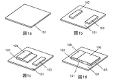
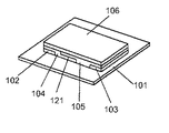
絶縁基板101と、
前記基板の表面上で互いに離間した少なくとも2つの電荷収集体102、103と、
プロトン電荷キャリアを生成するように構成されたプロトン生成電極層104と、
前記生成されたプロトン電荷キャリアを受容するように構成されたプロトン受容電極層105とを備える。
プロトン生成電極層104およびプロトン受容電極層105はそれぞれ、電荷収集体102、103のうちの対応するものに電気的に接続されるように構成され、プロトン生成電極層104とプロトン受容電極層105との間で電荷キャリアの移動が可能となるように接合領域において重複するように構成されることで電圧が形成される。
絶縁基板201と、
前記基板の表面上で互いに離間した少なくとも2つの電荷収集体202、203と、
プロトン電荷キャリアを生成するように構成されたプロトン生成電極層205と、
前記生成されたプロトン電荷キャリアを受容するように構成されたプロトン受容電極層204とを備える。
プロトン生成電極層205およびプロトン受容電極層204はそれぞれ、電荷収集体202、203のうちの対応するものに電気的に接続されるように構成され、プロトン生成電極層205とプロトン受容電極層204との間で電荷キャリアの移動が可能となるように接合領域において重複するように構成されることで電圧が形成される。
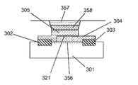
ここでは紙製である絶縁基板301と、
前記基板の表面上で互いに離間した少なくとも2つの電荷収集体302、303と、
プロトン電荷キャリアを生成するように構成されたプロトン生成電極層305と、
前記生成されたプロトン電荷キャリアを受容するように構成されたプロトン受容電極層304とを備える。
プロトン生成電極層305およびプロトン受容電極層304はそれぞれ、電荷収集体302、303のうちの対応するものに電気的に接続されるように構成され、プロトン生成電極層305とプロトン受容電極層304との間で電荷キャリアの移動が可能となるように接合領域において重複するように構成されることで電圧が形成される。
Claims (19)
- 絶縁基板と、
前記基板の表面上で互いに離間した少なくとも2つの電荷収集体と、
プロトン電荷キャリアを生成するように構成されたプロトン生成電極層と、
前記生成されたプロトン電荷キャリアを受容するように構成されたプロトン受容電極層とを備える装置であって、
前記プロトン生成電極層および前記プロトン受容電極層はそれぞれ、前記電荷収集体のうちの対応するものに電気的に接続されるように構成され、前記プロトン生成電極層と前記プロトン受容電極層との間で電荷キャリアの移動が可能となるように接合領域において重複するように構成されることで電圧が形成される、装置。 - 前記プロトン生成電極層は、酸化グラフェンを含む、請求項1に記載の装置。
- 前記プロトン受容電極層は、還元型酸化グラフェンを含む、請求項1または2に記載の装置。
- 前記電極層の少なくとも一方は、複数の完全または部分酸化グラフェンフレークを1つ以上含む、請求項1から3のいずれか一項に記載の装置。
- 前記プロトン電荷キャリアは、カルボキシ基、ヒドロキシ基、エポキシ基のうち、1つ以上を含む電荷分離官能基により生成される、請求項1から4のいずれか一項に記載の装置。
- 前記基板は、可撓性基板、弾性基板、折り畳み基板のうち少なくとも1つである、請求項1から5のいずれか一項に記載の装置。
- 前記基板は、ポリマーシートとガラスのうち少なくとも1つを含む、請求項1から6のいずれか一項に記載の装置。
- 前記基板は、紙を含む、請求項1から7のいずれか一項に記載の装置。
- 前記電荷収集体の少なくとも1つは、銀または銅を含む、請求項1から8のいずれか一項に記載の装置。
- 前記各電荷収集体と前記各電極層のうち少なくとも1つは、前記基板上に印刷される、請求項1から9のいずれか一項に記載の装置。
- 前記各電荷収集体と前記各電極層のうち少なくとも1つは、インクから形成される、請求項1から10のいずれか一項に記載の装置。
- 前記装置は、電解質層を含む、請求項1から11のいずれか一項に記載の装置。
- 前記電解質層は、ナフィオン(登録商標)またはポリビニルアルコールフィルムを含む、請求項12に記載の装置。
- 前記装置は、少なくとも前記プロトン生成電極層を被覆し、流体不透過性の材料を含有する保護層を含む、請求項1から13のいずれか一項に記載の装置。
- 前記装置は、バッテリーセル、電界効果トランジスタ(Field Effect Transistor:FET)、センサのうち、1つ以上を含む、請求項1から14のいずれか一項に記載の装置。
- 前記プロトン生成電極層は、存在する流体に応じてプロトン電荷キャリアを生成し、形成された前記電圧によって存在する流体の量を示すように構成される、請求項1から15のいずれか一項に記載の装置。
- 互いに接続された請求項1に記載の装置の配列を有するデバイスであって、
前記互いに接続された複数の装置は、共通基板に配列され、前記複数の装置が連動して累積的な効果が得られるよう互いに接続された、デバイス。 - 絶縁基板を設ける工程と、
前記基板の表面上で互いに離間した少なくとも2つの電荷収集体を設ける工程と、
プロトン電荷キャリアを生成するように構成されたプロトン生成電極層を設ける工程と、
前記生成されたプロトン電荷キャリアを受容するように構成されたプロトン受容電極層を設ける工程とを含む装置を製造する方法であって、
前記プロトン生成電極層および前記プロトン受容電極層はそれぞれ、前記電荷収集体のうちの対応するものに電気的に接続されるように構成され、前記プロトン生成電極層と前記プロトン受容電極層との間で電荷キャリアの移動が可能となるように接合領域において重複するように構成されることで電圧が形成される、方法。 - 前記各電荷収集体と前記各電極層のうち少なくとも1つが、印刷処理により前記基板上に設けられる、請求項18に記載の方法。
Applications Claiming Priority (3)
| Application Number | Priority Date | Filing Date | Title |
|---|---|---|---|
| GB1322029.8A GB2521193A (en) | 2013-12-12 | 2013-12-12 | Electronic apparatus and associated methods |
| GB1322029.8 | 2013-12-12 | ||
| PCT/FI2014/050835 WO2015086888A1 (en) | 2013-12-12 | 2014-11-06 | Electronic apparatus and associated methods |
Publications (2)
| Publication Number | Publication Date |
|---|---|
| JP2017511563A true JP2017511563A (ja) | 2017-04-20 |
| JP6234581B2 JP6234581B2 (ja) | 2017-11-22 |
Family
ID=50030853
Family Applications (1)
| Application Number | Title | Priority Date | Filing Date |
|---|---|---|---|
| JP2016536828A Expired - Fee Related JP6234581B2 (ja) | 2013-12-12 | 2014-11-06 | 電子装置および関連方法 |
Country Status (6)
| Country | Link |
|---|---|
| US (1) | US9859570B2 (ja) |
| EP (1) | EP3080597B1 (ja) |
| JP (1) | JP6234581B2 (ja) |
| GB (1) | GB2521193A (ja) |
| PL (1) | PL3080597T3 (ja) |
| WO (1) | WO2015086888A1 (ja) |
Cited By (1)
| Publication number | Priority date | Publication date | Assignee | Title |
|---|---|---|---|---|
| JP2023139750A (ja) * | 2022-03-22 | 2023-10-04 | 株式会社東芝 | 抗酸化剤を用いたfetセンサ |
Families Citing this family (10)
| Publication number | Priority date | Publication date | Assignee | Title |
|---|---|---|---|---|
| EP3007266B1 (en) * | 2014-10-07 | 2017-09-06 | Nokia Technologies OY | An apparatus and associated methods for electrical storage |
| EP3054433B1 (en) * | 2015-02-06 | 2018-08-29 | Nokia Technologies OY | Apparatus for detecting humidity |
| EP3145003B1 (en) | 2015-09-18 | 2019-09-04 | Nokia Technologies Oy | An apparatus and method of providing an apparatus for use as a power source |
| EP3260860A1 (en) * | 2016-06-23 | 2017-12-27 | Nokia Technologies Oy | Apparatus comprising a graphene based sensor and method of using the apparatus |
| EP3376553A1 (en) * | 2017-03-17 | 2018-09-19 | Nokia Technologies Oy | An apparatus and associated methods for electrical storage |
| KR101958302B1 (ko) * | 2017-10-11 | 2019-03-15 | 한국전력공사 | 슈퍼커패시터용 그래핀 전극의 제조 방법 |
| IT201800000791A1 (it) | 2018-01-12 | 2019-07-12 | Gqenergy Srl | Generatore elettrico |
| CN108593717A (zh) * | 2018-04-26 | 2018-09-28 | 京东方科技集团股份有限公司 | 一种湿度传感器及其制作方法、电子设备 |
| US11283096B2 (en) * | 2019-05-22 | 2022-03-22 | Arborsense, Inc. | Fabrication process for making electrochemical multilayer membrane matertals |
| CN113422094B (zh) * | 2021-06-07 | 2023-03-24 | 李慧虹 | 凝胶浓差产电器件及其制备方法 |
Citations (2)
| Publication number | Priority date | Publication date | Assignee | Title |
|---|---|---|---|---|
| JP2012015481A (ja) * | 2010-06-01 | 2012-01-19 | Sony Corp | 電界効果トランジスタの製造方法、電界効果トランジスタおよび半導体酸化グラフェンの製造方法 |
| US20130313523A1 (en) * | 2012-05-22 | 2013-11-28 | Electronics And Telecommunications Research Institute | Graphene electronic device and method of fabricating the same |
Family Cites Families (17)
| Publication number | Priority date | Publication date | Assignee | Title |
|---|---|---|---|---|
| GB8322418D0 (en) * | 1983-08-19 | 1983-09-21 | Emi Ltd | Humidity sensor |
| US4894301A (en) | 1989-08-03 | 1990-01-16 | Bell Communications Research, Inc. | Battery containing solid protonically conducting electrolyte |
| US5731105A (en) | 1993-09-07 | 1998-03-24 | E.C.R. - Electro-Chemical Research Ltd. | Battery electrochemical cell with a non-liquid electrolyte |
| US6576365B1 (en) * | 1999-12-06 | 2003-06-10 | E.C.R. - Electro Chemical Research Ltd. | Ultra-thin electrochemical energy storage devices |
| JP4196374B2 (ja) * | 2001-03-29 | 2008-12-17 | パナソニック株式会社 | 高分子電解質型薄膜燃料電池およびその運転方法 |
| CA2483815A1 (en) * | 2002-04-23 | 2003-11-06 | Uwe Guntow | High-temperature solid electrolyte fuel cell comprising a composite of nanoporous thin-film electrodes and a structured electrolyte |
| US20040053100A1 (en) * | 2002-09-12 | 2004-03-18 | Stanley Kevin G. | Method of fabricating fuel cells and membrane electrode assemblies |
| US20040076868A1 (en) * | 2002-10-18 | 2004-04-22 | Peter Mardilovich | Fuel cell and method for forming |
| GB2449926A (en) * | 2007-06-08 | 2008-12-10 | Seiko Epson Corp | Method for manufacturing an electrolyte pattern |
| FR2951876B1 (fr) * | 2009-10-26 | 2012-02-03 | Commissariat Energie Atomique | Micro-batterie au lithium munie d'une couche d'encapsulation conductrice electroniquement |
| KR101851565B1 (ko) | 2011-08-17 | 2018-04-25 | 삼성전자주식회사 | 트랜지스터와 그 제조방법 및 트랜지스터를 포함하는 전자소자 |
| JP6009343B2 (ja) * | 2011-12-26 | 2016-10-19 | 株式会社半導体エネルギー研究所 | 二次電池用正極および二次電池用正極の作製方法 |
| JP6077347B2 (ja) * | 2012-04-10 | 2017-02-08 | 株式会社半導体エネルギー研究所 | 非水系二次電池用正極の製造方法 |
| KR101920714B1 (ko) * | 2012-05-16 | 2018-11-21 | 삼성전자주식회사 | 리튬 전지용 음극 및 이를 포함하는 리튬 전지 |
| US20130314844A1 (en) * | 2012-05-23 | 2013-11-28 | Nanyang Technological University | Method of preparing reduced graphene oxide foam |
| EP2667417A1 (en) * | 2012-05-23 | 2013-11-27 | Imec | Graphene-based semiconductor device |
| US9728771B2 (en) * | 2013-05-23 | 2017-08-08 | Nokia Technologies Oy | Proton-battery based on graphene derivatives |
-
2013
- 2013-12-12 GB GB1322029.8A patent/GB2521193A/en not_active Withdrawn
-
2014
- 2014-11-06 EP EP14869206.4A patent/EP3080597B1/en not_active Not-in-force
- 2014-11-06 JP JP2016536828A patent/JP6234581B2/ja not_active Expired - Fee Related
- 2014-11-06 WO PCT/FI2014/050835 patent/WO2015086888A1/en not_active Ceased
- 2014-11-06 US US15/037,305 patent/US9859570B2/en not_active Expired - Fee Related
- 2014-11-06 PL PL14869206T patent/PL3080597T3/pl unknown
Patent Citations (2)
| Publication number | Priority date | Publication date | Assignee | Title |
|---|---|---|---|---|
| JP2012015481A (ja) * | 2010-06-01 | 2012-01-19 | Sony Corp | 電界効果トランジスタの製造方法、電界効果トランジスタおよび半導体酸化グラフェンの製造方法 |
| US20130313523A1 (en) * | 2012-05-22 | 2013-11-28 | Electronics And Telecommunications Research Institute | Graphene electronic device and method of fabricating the same |
Non-Patent Citations (1)
| Title |
|---|
| 緒方盟子、外5名: "酸化グラフェン燃料電池(GOFC)", 電気化学会大会講演要旨集, vol. 80, JPN6017026106, 29 March 2013 (2013-03-29), JP, pages 295ページ, ISSN: 0003599276 * |
Cited By (1)
| Publication number | Priority date | Publication date | Assignee | Title |
|---|---|---|---|---|
| JP2023139750A (ja) * | 2022-03-22 | 2023-10-04 | 株式会社東芝 | 抗酸化剤を用いたfetセンサ |
Also Published As
| Publication number | Publication date |
|---|---|
| US20160293973A1 (en) | 2016-10-06 |
| EP3080597A1 (en) | 2016-10-19 |
| GB201322029D0 (en) | 2014-01-29 |
| US9859570B2 (en) | 2018-01-02 |
| PL3080597T3 (pl) | 2019-01-31 |
| EP3080597A4 (en) | 2017-06-14 |
| JP6234581B2 (ja) | 2017-11-22 |
| EP3080597B1 (en) | 2018-09-05 |
| GB2521193A (en) | 2015-06-17 |
| WO2015086888A1 (en) | 2015-06-18 |
Similar Documents
| Publication | Publication Date | Title |
|---|---|---|
| JP6234581B2 (ja) | 電子装置および関連方法 | |
| Say et al. | Spray-coated paper supercapacitors | |
| Manjakkal et al. | Energy autonomous sweat‐based wearable systems | |
| Wei et al. | Flexible iontronics based on 2D nanofluidic material | |
| Manjakkal et al. | Flexible self-charging supercapacitor based on graphene-Ag-3D graphene foam electrodes | |
| Khatib et al. | Self‐healing soft sensors: from material design to implementation | |
| Zu et al. | Electrochemical power generation humidity sensor based on WS2 nanoflakes | |
| Liang et al. | Electric power generation via asymmetric moisturizing of graphene oxide for flexible, printable and portable electronics | |
| Weng et al. | Self-chargeable supercapacitor made with MXene-bacterial cellulose nanofiber composite for wearable devices | |
| Bocchetta et al. | Soft materials for wearable/flexible electrochemical energy conversion, storage, and biosensor devices | |
| Zhang et al. | Flexible supercapacitors based on paper substrates: a new paradigm for low-cost energy storage | |
| Banerjee et al. | Capacitor to supercapacitor | |
| CN105393385B (zh) | 基于石墨烯衍生物的质子电池 | |
| EP3007266B1 (en) | An apparatus and associated methods for electrical storage | |
| Wei | Writable electrochemical energy source based on graphene oxide | |
| JP6483286B2 (ja) | 蓄電装置及びこれに関する方法 | |
| Ren et al. | An ultrastretchable seamlessly integrated contactless charging microsystem towards skin-attachable wireless microelectronics | |
| Kumar et al. | Recent progress and challenges in paper-based microsupercapacitors for flexible electronics: a comprehensive review | |
| Cai et al. | A recyclable triboelectric nanogenerator integrated into insole for sensing human motion | |
| CN105612419B (zh) | 用于分析物检测的装置和相关联的方法 | |
| US10297838B2 (en) | Method of forming a graphene oxide-reduced graphene oxide junction | |
| Ren et al. | 3D-printed stretchable modular integrated microsystems toward sweat monitoring powered by wireless charging sodium-ion micro-batteries | |
| Baruah et al. | Layered MXene-transition metal oxide nanocomposite revealing its versatility in methanol oxidation and PVA/KOH hydrogel-based symmetric supercapacitor | |
| Chen et al. | Conductive Paper and Its Applications | |
| Liu et al. | Graphene-based planar on-chip micro-supercapacitors with whole series/parallel configuration for integration |
Legal Events
| Date | Code | Title | Description |
|---|---|---|---|
| A621 | Written request for application examination |
Free format text: JAPANESE INTERMEDIATE CODE: A621 Effective date: 20160620 |
|
| A131 | Notification of reasons for refusal |
Free format text: JAPANESE INTERMEDIATE CODE: A131 Effective date: 20170713 |
|
| A521 | Request for written amendment filed |
Free format text: JAPANESE INTERMEDIATE CODE: A523 Effective date: 20170915 |
|
| TRDD | Decision of grant or rejection written | ||
| A01 | Written decision to grant a patent or to grant a registration (utility model) |
Free format text: JAPANESE INTERMEDIATE CODE: A01 Effective date: 20171011 |
|
| A61 | First payment of annual fees (during grant procedure) |
Free format text: JAPANESE INTERMEDIATE CODE: A61 Effective date: 20171024 |
|
| R150 | Certificate of patent or registration of utility model |
Ref document number: 6234581 Country of ref document: JP Free format text: JAPANESE INTERMEDIATE CODE: R150 |
|
| R250 | Receipt of annual fees |
Free format text: JAPANESE INTERMEDIATE CODE: R250 |
|
| R250 | Receipt of annual fees |
Free format text: JAPANESE INTERMEDIATE CODE: R250 |
|
| LAPS | Cancellation because of no payment of annual fees |