JP2017502496A - High density linear capacitor - Google Patents
High density linear capacitor Download PDFInfo
- Publication number
- JP2017502496A JP2017502496A JP2016527204A JP2016527204A JP2017502496A JP 2017502496 A JP2017502496 A JP 2017502496A JP 2016527204 A JP2016527204 A JP 2016527204A JP 2016527204 A JP2016527204 A JP 2016527204A JP 2017502496 A JP2017502496 A JP 2017502496A
- Authority
- JP
- Japan
- Prior art keywords
- capacitor structure
- polysilicon structures
- wirings
- polysilicon
- wiring
- Prior art date
- Legal status (The legal status is an assumption and is not a legal conclusion. Google has not performed a legal analysis and makes no representation as to the accuracy of the status listed.)
- Pending
Links
- 239000003990 capacitor Substances 0.000 title claims abstract description 107
- 229910021420 polycrystalline silicon Inorganic materials 0.000 claims abstract description 67
- 229920005591 polysilicon Polymers 0.000 claims abstract description 67
- 238000000034 method Methods 0.000 claims abstract description 42
- 239000004065 semiconductor Substances 0.000 claims abstract description 38
- 239000000758 substrate Substances 0.000 claims abstract description 34
- 238000009792 diffusion process Methods 0.000 claims abstract description 14
- 238000004891 communication Methods 0.000 claims description 12
- 238000007667 floating Methods 0.000 claims description 5
- 238000002955 isolation Methods 0.000 claims description 4
- 238000003860 storage Methods 0.000 description 29
- 239000010410 layer Substances 0.000 description 27
- 238000013461 design Methods 0.000 description 22
- 230000008569 process Effects 0.000 description 14
- 230000015654 memory Effects 0.000 description 11
- 230000006870 function Effects 0.000 description 9
- 238000010586 diagram Methods 0.000 description 8
- 238000004519 manufacturing process Methods 0.000 description 7
- 239000000463 material Substances 0.000 description 6
- 239000002184 metal Substances 0.000 description 6
- 229910052751 metal Inorganic materials 0.000 description 6
- 230000015572 biosynthetic process Effects 0.000 description 4
- 238000005516 engineering process Methods 0.000 description 4
- 230000003287 optical effect Effects 0.000 description 4
- 239000000203 mixture Substances 0.000 description 3
- 238000013459 approach Methods 0.000 description 2
- 238000004590 computer program Methods 0.000 description 2
- 239000010949 copper Substances 0.000 description 2
- 239000003989 dielectric material Substances 0.000 description 2
- 239000000835 fiber Substances 0.000 description 2
- 239000011810 insulating material Substances 0.000 description 2
- 238000001459 lithography Methods 0.000 description 2
- 238000012986 modification Methods 0.000 description 2
- 230000004048 modification Effects 0.000 description 2
- 238000000623 plasma-assisted chemical vapour deposition Methods 0.000 description 2
- RYGMFSIKBFXOCR-UHFFFAOYSA-N Copper Chemical compound [Cu] RYGMFSIKBFXOCR-UHFFFAOYSA-N 0.000 description 1
- 230000005540 biological transmission Effects 0.000 description 1
- 230000001143 conditioned effect Effects 0.000 description 1
- 239000004020 conductor Substances 0.000 description 1
- 238000010276 construction Methods 0.000 description 1
- 229910052802 copper Inorganic materials 0.000 description 1
- 230000008878 coupling Effects 0.000 description 1
- 238000010168 coupling process Methods 0.000 description 1
- 238000005859 coupling reaction Methods 0.000 description 1
- 239000002019 doping agent Substances 0.000 description 1
- 230000009977 dual effect Effects 0.000 description 1
- 230000005684 electric field Effects 0.000 description 1
- 238000000609 electron-beam lithography Methods 0.000 description 1
- 238000002513 implantation Methods 0.000 description 1
- 238000009413 insulation Methods 0.000 description 1
- 239000012212 insulator Substances 0.000 description 1
- 239000011229 interlayer Substances 0.000 description 1
- 230000007787 long-term memory Effects 0.000 description 1
- 229910044991 metal oxide Inorganic materials 0.000 description 1
- 150000004706 metal oxides Chemical class 0.000 description 1
- 230000008520 organization Effects 0.000 description 1
- 238000000059 patterning Methods 0.000 description 1
- 238000000206 photolithography Methods 0.000 description 1
- 230000006403 short-term memory Effects 0.000 description 1
- 238000004088 simulation Methods 0.000 description 1
- 125000006850 spacer group Chemical group 0.000 description 1
- 238000006467 substitution reaction Methods 0.000 description 1
- 238000012546 transfer Methods 0.000 description 1
- WFKWXMTUELFFGS-UHFFFAOYSA-N tungsten Chemical compound [W] WFKWXMTUELFFGS-UHFFFAOYSA-N 0.000 description 1
- 229910052721 tungsten Inorganic materials 0.000 description 1
- 239000010937 tungsten Substances 0.000 description 1
- 238000012795 verification Methods 0.000 description 1
Images


Classifications
-
- H—ELECTRICITY
- H01—ELECTRIC ELEMENTS
- H01L—SEMICONDUCTOR DEVICES NOT COVERED BY CLASS H10
- H01L27/00—Devices consisting of a plurality of semiconductor or other solid-state components formed in or on a common substrate
- H01L27/02—Devices consisting of a plurality of semiconductor or other solid-state components formed in or on a common substrate including semiconductor components specially adapted for rectifying, oscillating, amplifying or switching and having potential barriers; including integrated passive circuit elements having potential barriers
- H01L27/04—Devices consisting of a plurality of semiconductor or other solid-state components formed in or on a common substrate including semiconductor components specially adapted for rectifying, oscillating, amplifying or switching and having potential barriers; including integrated passive circuit elements having potential barriers the substrate being a semiconductor body
- H01L27/06—Devices consisting of a plurality of semiconductor or other solid-state components formed in or on a common substrate including semiconductor components specially adapted for rectifying, oscillating, amplifying or switching and having potential barriers; including integrated passive circuit elements having potential barriers the substrate being a semiconductor body including a plurality of individual components in a non-repetitive configuration
- H01L27/0611—Devices consisting of a plurality of semiconductor or other solid-state components formed in or on a common substrate including semiconductor components specially adapted for rectifying, oscillating, amplifying or switching and having potential barriers; including integrated passive circuit elements having potential barriers the substrate being a semiconductor body including a plurality of individual components in a non-repetitive configuration integrated circuits having a two-dimensional layout of components without a common active region
- H01L27/0617—Devices consisting of a plurality of semiconductor or other solid-state components formed in or on a common substrate including semiconductor components specially adapted for rectifying, oscillating, amplifying or switching and having potential barriers; including integrated passive circuit elements having potential barriers the substrate being a semiconductor body including a plurality of individual components in a non-repetitive configuration integrated circuits having a two-dimensional layout of components without a common active region comprising components of the field-effect type
- H01L27/0629—Devices consisting of a plurality of semiconductor or other solid-state components formed in or on a common substrate including semiconductor components specially adapted for rectifying, oscillating, amplifying or switching and having potential barriers; including integrated passive circuit elements having potential barriers the substrate being a semiconductor body including a plurality of individual components in a non-repetitive configuration integrated circuits having a two-dimensional layout of components without a common active region comprising components of the field-effect type in combination with diodes, or resistors, or capacitors
-
- H—ELECTRICITY
- H01—ELECTRIC ELEMENTS
- H01L—SEMICONDUCTOR DEVICES NOT COVERED BY CLASS H10
- H01L23/00—Details of semiconductor or other solid state devices
- H01L23/52—Arrangements for conducting electric current within the device in operation from one component to another, i.e. interconnections, e.g. wires, lead frames
- H01L23/522—Arrangements for conducting electric current within the device in operation from one component to another, i.e. interconnections, e.g. wires, lead frames including external interconnections consisting of a multilayer structure of conductive and insulating layers inseparably formed on the semiconductor body
- H01L23/5222—Capacitive arrangements or effects of, or between wiring layers
- H01L23/5223—Capacitor integral with wiring layers
-
- H—ELECTRICITY
- H01—ELECTRIC ELEMENTS
- H01L—SEMICONDUCTOR DEVICES NOT COVERED BY CLASS H10
- H01L27/00—Devices consisting of a plurality of semiconductor or other solid-state components formed in or on a common substrate
- H01L27/02—Devices consisting of a plurality of semiconductor or other solid-state components formed in or on a common substrate including semiconductor components specially adapted for rectifying, oscillating, amplifying or switching and having potential barriers; including integrated passive circuit elements having potential barriers
- H01L27/04—Devices consisting of a plurality of semiconductor or other solid-state components formed in or on a common substrate including semiconductor components specially adapted for rectifying, oscillating, amplifying or switching and having potential barriers; including integrated passive circuit elements having potential barriers the substrate being a semiconductor body
- H01L27/06—Devices consisting of a plurality of semiconductor or other solid-state components formed in or on a common substrate including semiconductor components specially adapted for rectifying, oscillating, amplifying or switching and having potential barriers; including integrated passive circuit elements having potential barriers the substrate being a semiconductor body including a plurality of individual components in a non-repetitive configuration
- H01L27/07—Devices consisting of a plurality of semiconductor or other solid-state components formed in or on a common substrate including semiconductor components specially adapted for rectifying, oscillating, amplifying or switching and having potential barriers; including integrated passive circuit elements having potential barriers the substrate being a semiconductor body including a plurality of individual components in a non-repetitive configuration the components having an active region in common
- H01L27/0705—Devices consisting of a plurality of semiconductor or other solid-state components formed in or on a common substrate including semiconductor components specially adapted for rectifying, oscillating, amplifying or switching and having potential barriers; including integrated passive circuit elements having potential barriers the substrate being a semiconductor body including a plurality of individual components in a non-repetitive configuration the components having an active region in common comprising components of the field effect type
- H01L27/0727—Devices consisting of a plurality of semiconductor or other solid-state components formed in or on a common substrate including semiconductor components specially adapted for rectifying, oscillating, amplifying or switching and having potential barriers; including integrated passive circuit elements having potential barriers the substrate being a semiconductor body including a plurality of individual components in a non-repetitive configuration the components having an active region in common comprising components of the field effect type in combination with diodes, or capacitors or resistors
- H01L27/0733—Devices consisting of a plurality of semiconductor or other solid-state components formed in or on a common substrate including semiconductor components specially adapted for rectifying, oscillating, amplifying or switching and having potential barriers; including integrated passive circuit elements having potential barriers the substrate being a semiconductor body including a plurality of individual components in a non-repetitive configuration the components having an active region in common comprising components of the field effect type in combination with diodes, or capacitors or resistors in combination with capacitors only
-
- H—ELECTRICITY
- H01—ELECTRIC ELEMENTS
- H01L—SEMICONDUCTOR DEVICES NOT COVERED BY CLASS H10
- H01L28/00—Passive two-terminal components without a potential-jump or surface barrier for integrated circuits; Details thereof; Multistep manufacturing processes therefor
- H01L28/40—Capacitors
- H01L28/60—Electrodes
- H01L28/82—Electrodes with an enlarged surface, e.g. formed by texturisation
- H01L28/86—Electrodes with an enlarged surface, e.g. formed by texturisation having horizontal extensions
-
- H—ELECTRICITY
- H01—ELECTRIC ELEMENTS
- H01L—SEMICONDUCTOR DEVICES NOT COVERED BY CLASS H10
- H01L28/00—Passive two-terminal components without a potential-jump or surface barrier for integrated circuits; Details thereof; Multistep manufacturing processes therefor
- H01L28/40—Capacitors
- H01L28/60—Electrodes
- H01L28/82—Electrodes with an enlarged surface, e.g. formed by texturisation
- H01L28/90—Electrodes with an enlarged surface, e.g. formed by texturisation having vertical extensions
- H01L28/92—Electrodes with an enlarged surface, e.g. formed by texturisation having vertical extensions made by patterning layers, e.g. by etching conductive layers
-
- H—ELECTRICITY
- H01—ELECTRIC ELEMENTS
- H01L—SEMICONDUCTOR DEVICES NOT COVERED BY CLASS H10
- H01L29/00—Semiconductor devices specially adapted for rectifying, amplifying, oscillating or switching and having potential barriers; Capacitors or resistors having potential barriers, e.g. a PN-junction depletion layer or carrier concentration layer; Details of semiconductor bodies or of electrodes thereof ; Multistep manufacturing processes therefor
- H01L29/66—Types of semiconductor device ; Multistep manufacturing processes therefor
- H01L29/66007—Multistep manufacturing processes
- H01L29/66075—Multistep manufacturing processes of devices having semiconductor bodies comprising group 14 or group 13/15 materials
- H01L29/66227—Multistep manufacturing processes of devices having semiconductor bodies comprising group 14 or group 13/15 materials the devices being controllable only by the electric current supplied or the electric potential applied, to an electrode which does not carry the current to be rectified, amplified or switched, e.g. three-terminal devices
- H01L29/66409—Unipolar field-effect transistors
- H01L29/66477—Unipolar field-effect transistors with an insulated gate, i.e. MISFET
- H01L29/66787—Unipolar field-effect transistors with an insulated gate, i.e. MISFET with a gate at the side of the channel
- H01L29/66795—Unipolar field-effect transistors with an insulated gate, i.e. MISFET with a gate at the side of the channel with a horizontal current flow in a vertical sidewall of a semiconductor body, e.g. FinFET, MuGFET
-
- H—ELECTRICITY
- H01—ELECTRIC ELEMENTS
- H01L—SEMICONDUCTOR DEVICES NOT COVERED BY CLASS H10
- H01L2924/00—Indexing scheme for arrangements or methods for connecting or disconnecting semiconductor or solid-state bodies as covered by H01L24/00
- H01L2924/0001—Technical content checked by a classifier
- H01L2924/0002—Not covered by any one of groups H01L24/00, H01L24/00 and H01L2224/00
Landscapes
- Engineering & Computer Science (AREA)
- Power Engineering (AREA)
- Computer Hardware Design (AREA)
- Microelectronics & Electronic Packaging (AREA)
- Physics & Mathematics (AREA)
- Condensed Matter Physics & Semiconductors (AREA)
- General Physics & Mathematics (AREA)
- Semiconductor Integrated Circuits (AREA)
- Internal Circuitry In Semiconductor Integrated Circuit Devices (AREA)
- Metal-Oxide And Bipolar Metal-Oxide Semiconductor Integrated Circuits (AREA)
Abstract
キャパシタ構造を作製するための方法は、半導体基板上にポリシリコン構造を作製するステップを含む。本方法は、半導体基板上にM1−拡散(MD)配線を作製するステップをさらに含む。ポリシリコン構造はMD配線を備えたインターリーブ構成で配設される。本方法はまた、キャパシタ構造として、MD配線および/またはポリシリコン構造のインターリーブ構成を選択的に接続するステップを含む。A method for fabricating a capacitor structure includes fabricating a polysilicon structure on a semiconductor substrate. The method further includes fabricating M1-diffusion (MD) wiring on the semiconductor substrate. The polysilicon structure is arranged in an interleaved configuration with MD wiring. The method also includes selectively connecting an MD interconnect and / or an interleaved structure of a polysilicon structure as the capacitor structure.
Description
(関連出願の相互参照)
本開示は、その開示の全体が参照により本明細書に明示的に組み込まれている、2013年11月20日に出願した、「HIGH DENSITY LINEAR CAPACITOR」という名称の米国仮特許出願第61/906,834号の利益を主張するものである。
(Cross-reference of related applications)
This disclosure is a US Provisional Patent Application No. 61/906, filed Nov. 20, 2013, entitled “HIGH DENSITY LINEAR CAPACITOR,” the entire disclosure of which is expressly incorporated herein by reference. , 834 claims the profit.
本開示の態様は、半導体デバイスに関し、より詳細には、半導体構造内のキャパシタに関する。 Aspects of the present disclosure relate to semiconductor devices and, more particularly, to capacitors in semiconductor structures.
混合信号/無線周波数(RF)回路内で、密度が増加した線形キャパシタは、領域を削減することが望ましい。回転金属酸化物金属(RTMOM:rotated metal−oxide−metal)およびフィンガー金属酸化物金属(FMOM:finger metal−oxide−metal)など、金属キャパシタを使用することが可能である。しかしながら、それらの密度は、非線形である金属酸化物半導体(MOS)キャパシタの密度よりもはるかに低い。 In mixed signal / radio frequency (RF) circuits, linear capacitors with increased density are desirable to reduce area. Metal capacitors, such as rotating metal-oxide-metal (RTMOM) and finger metal-oxide-metal (FMOM), can be used. However, their density is much lower than the density of non-linear metal oxide semiconductor (MOS) capacitors.
キャパシタ構造を作製するための方法は、半導体基板上にポリシリコン構造を作製するステップを含む。本方法は、半導体基板上にM1−拡散(MD:M1 to diffusion)配線を作製するステップをさらに含む。ポリシリコン構造はMD配線を備えたインターリーブ構成で配設される。本方法はまた、キャパシタ構造として、MD配線および/またはポリシリコン構造のインターリーブ構成を選択的に接続するステップを含む。 A method for fabricating a capacitor structure includes fabricating a polysilicon structure on a semiconductor substrate. The method further includes fabricating an M1-Diffusion (MD) wiring on the semiconductor substrate. The polysilicon structure is arranged in an interleaved configuration with MD wiring. The method also includes selectively connecting an MD interconnect and / or an interleaved structure of polysilicon structure as the capacitor structure.
キャパシタ構造は、半導体基板上のポリシリコン構造を含む。本構造はまた、半導体基板上のM1−拡散(MD)配線を含む。ポリシリコン構造はMD配線を備えたインターリーブ構成で配設される。MD配線および/またはポリシリコン構造は、キャパシタ構造としてインターリーブ構成で選択的に接続される。 The capacitor structure includes a polysilicon structure on a semiconductor substrate. The structure also includes M1-diffusion (MD) wiring on the semiconductor substrate. The polysilicon structure is arranged in an interleaved configuration with MD wiring. The MD wiring and / or the polysilicon structure are selectively connected as a capacitor structure in an interleaved configuration.
キャパシタ構造は、半導体基板上のポリシリコン構造を含む。キャパシタ構造は、半導体基板上の酸化物拡散領域に導電層を配線するための手段を含む。ポリシリコン構造は、配線手段を備えたインターリーブ構成で配設される。ポリシリコン構造および/または配線手段は、キャパシタ構造としてインターリーブ構成で選択的に接続される。 The capacitor structure includes a polysilicon structure on a semiconductor substrate. The capacitor structure includes means for wiring a conductive layer in the oxide diffusion region on the semiconductor substrate. The polysilicon structure is arranged in an interleaved configuration with wiring means. The polysilicon structure and / or the wiring means are selectively connected in an interleaved configuration as a capacitor structure.
上記は、続く詳細な説明をよりよく理解することができるように、本開示の特徴および技術的利点について、かなり大まかに概説したものである。本開示のさらなる特徴および利点について、以下で説明する。本開示は、本開示と同じ目的を果たすための他の構造を修正または設計する基礎として容易に利用できることを、当業者には理解されたい。そのような等価な構造(construction)が、添付の特許請求の範囲に記載の本開示の教示から逸脱しないことも、当業者には理解されたい。本開示の特徴になると考えられる新規な特徴は、本開示の構成(organization)と動作方法の両方に関して、さらなる目的および利点とともに、以下の説明を添付の図と併せ検討することからよりよく理解されるであろう。しかしながら、図の各々は、例示および説明を目的として提供されているに過ぎず、本開示の制限を定めるものではないことを、明確に理解されたい。 The foregoing has outlined rather broadly the features and technical advantages of the present disclosure in order that the detailed description that follows may be better understood. Additional features and advantages of the present disclosure are described below. Those skilled in the art will appreciate that the present disclosure can be readily utilized as a basis for modifying or designing other structures to serve the same purpose as the present disclosure. It should also be understood by those skilled in the art that such equivalent constructions do not depart from the teachings of the present disclosure as set forth in the appended claims. The novel features believed to be features of the present disclosure will be better understood from a consideration of the following description in conjunction with the accompanying figures, along with further objects and advantages, both with regard to the organization and method of operation of the present disclosure. It will be. However, it should be clearly understood that each of the figures is provided for purposes of illustration and description only and does not define limitations of the present disclosure.
本開示のより完全な理解が得られるように、ここで、以下の説明を添付の図面と併せて参照する。 For a fuller understanding of the present disclosure, reference is now made to the following description, taken in conjunction with the accompanying drawings, in which:
添付の図面に関して以下に記載する詳細な説明は、様々な構成の説明として意図されており、本明細書で説明する概念が実践され得る構成のみを表すことは意図されていない。詳細な説明は、様々な概念の完全な理解を与える目的で特定の詳細を含む。しかしながら、これらの概念がこれらの具体的な詳細なしに実践され得ることが、当業者には明らかであろう。場合によっては、そのような概念を曖昧にすることを回避するために、よく知られている構造および構成要素がブロック図の形態で示されている。本明細書の説明では、「および/または」という用語の使用は、「包含的論理和」を表すことを意図し、「または」という用語の使用は、「排他的論理和」を表すことを意図する。 The detailed description set forth below in connection with the appended drawings is intended as a description of various configurations and is not intended to represent the only configurations in which the concepts described herein may be practiced. The detailed description includes specific details for the purpose of providing a thorough understanding of various concepts. However, it will be apparent to those skilled in the art that these concepts can be practiced without these specific details. In some instances, well-known structures and components are shown in block diagram form in order to avoid obscuring such concepts. In the description herein, the use of the term “and / or” is intended to mean “inclusive OR”, and the use of the term “or” means “exclusive OR”. Intended.
キャパシタは、電荷を蓄積するために集積回路内で使用される受動素子である。キャパシタは、プレート間の絶縁材料と導電性があるプレートまたは構造を使用して作られることが多い。所与のキャパシタ用の蓄積の量、すなわち、キャパシタンスは、それらのプレートおよび絶縁体を作るために使用される材料、プレートの面積、およびプレート間の間隔を条件とする。絶縁材料は誘電材料であることが多い。 A capacitor is a passive element used in an integrated circuit to store charge. Capacitors are often made using an insulating material between the plates and a conductive plate or structure. The amount of storage, or capacitance, for a given capacitor is conditioned on the material used to make those plates and insulators, the area of the plates, and the spacing between the plates. The insulating material is often a dielectric material.
キャパシタは、半導体チップ上の広い領域を消費し得るが、これは多くの設計はチップの基板上にキャパシタを配置するためである。この手法は、大量の基板領域を占有し、これは、能動デバイスに利用可能な領域を削減する。別の手法は、垂直平行板(VPP)キャパシタとして知られている場合がある垂直構造を作成することである。VPPキャパシタ構造は、チップ上の材料層の積層によって作成され得る。しかしながら、これらの構造はあまり多くの電荷を蓄積しないという点で、VPP構造はより低い容量性ストレージ、またはより低い「密度」を有する。この配線およびビア層導電性トレースはサイズの点で非常に小さい。VPP構造における配線とビア層導電性トレースとの間の間隔は設計規則によって制限され、これは、結果として、そのような構造に関してある種の所望されるキャパシタンスを達成するために広い領域をもたらすことが多い。「垂直」として説明するが、これらの構造は、基板の表面に対して実質的に直交する任意の方向、または半導体作製プロセスを使用して、基板に対して実質的に平行でない他の角度であり得る。 Capacitors can consume a large area on the semiconductor chip because many designs place the capacitors on the chip substrate. This approach occupies a large amount of substrate area, which reduces the area available for active devices. Another approach is to create a vertical structure, sometimes known as a vertical parallel plate (VPP) capacitor. A VPP capacitor structure can be created by stacking material layers on a chip. However, VPP structures have lower capacitive storage or lower “density” in that these structures do not accumulate too much charge. The wiring and via layer conductive traces are very small in size. The spacing between interconnects and via layer conductive traces in VPP structures is limited by design rules, which results in a large area to achieve some desired capacitance for such structures. There are many. Although described as “perpendicular”, these structures can be in any direction that is substantially perpendicular to the surface of the substrate, or other angle that is not substantially parallel to the substrate using a semiconductor fabrication process. possible.
半導体作製プロセスは、しばしば、3つの部分に分割される。すなわち、フロントエンドオブライン(FEOL:front end of line)、ミドルオブライン(MOL:middle of line)、およびバックエンドオブライン(BEOL:back end of line)である。フロントエンドオブラインプロセスは、ウエハ作成と、絶縁と、ウェル形成と、ゲートパターニングと、スペーサと、ドーパント注入とを含む。ミドルオブラインプロセスは、ゲートおよび端子コンタクト形成を含む。しかしながら、ミドルオブラインプロセスのゲートおよび端子コンタクト形成は、特にリソグラフィパターニングに関して、作製フローのますます困難な部分となっている。バックエンドオブラインプロセスは、FEOLデバイスに結合するための配線および誘電体層を形成することを含む。これらの配線は、プラズマ強化化学蒸着(PECVD)堆積層間絶縁(ILD)材料を使用してデュアルダマシンプロセスで作製され得る。 The semiconductor fabrication process is often divided into three parts. That is, a front end of line (FEOL), a middle of line (MOL), and a back end of line (BEOL). The front-end-of-line process includes wafer creation, insulation, well formation, gate patterning, spacers, and dopant implantation. The middle-of-line process includes gate and terminal contact formation. However, gate and terminal contact formation in the middle-of-line process has become an increasingly difficult part of the fabrication flow, especially with respect to lithographic patterning. The back-end-of-line process includes forming wiring and dielectric layers for coupling to FEOL devices. These interconnects can be made in a dual damascene process using plasma enhanced chemical vapor deposition (PECVD) deposited interlayer dielectric (ILD) materials.
より最近では、現在、近代のマイクロプロセッサ内で配線されている大量のトランジスタにより、回路用の配線レベルの数はかなり増大した。数が増大したトランジスタをサポートするために増大された数の配線レベルは、ゲートおよび端子接触形成を実行するために、より複雑なミドルオブラインプロセスに関連する。 More recently, the number of wiring levels for circuits has increased considerably due to the large number of transistors currently wired in modern microprocessors. The increased number of interconnect levels to support the increased number of transistors is associated with more complex middle-of-line processes to perform gate and terminal contact formation.
特に、リソグラフィの進歩は、集積回路チップ上のライン間隔を20ナノメートル未満に削減した。より多くのラインの電荷蓄積を同じ量の材料内に配置することができるため、これらの削減されたライン間隔の使用はキャパシタンスの利用可能な領域を増大する。さらに、ミドルオブライン配線構造の使用は、本開示の一態様で説明するように、改善されたキャパシタ構造を可能にする。 In particular, advances in lithography have reduced line spacing on integrated circuit chips to less than 20 nanometers. The use of these reduced line spacing increases the available area of capacitance because more lines of charge storage can be placed in the same amount of material. Further, the use of the middle-of-line wiring structure allows for an improved capacitor structure, as described in one aspect of the present disclosure.
本明細書で説明するように、ミドルオブライン配線層は、第1の導電層(たとえば、金属1(M1))を集積回路の酸化物拡散(OD)層に接続するため、ならびに、M1を集積回路の能動デバイスに接続するための導電配線を指す場合がある。M1を集積回路のOD層に接続するためのミドルオブライン配線層は、「MD1」および「MD2」と呼ばれる場合があり、これらは、本明細書で、集合的に「MD配線」と呼ばれる。M1を集積回路のポリシリコンゲートに接続するためのミドルオブライン配線層は、「MP」または「MP配線」と呼ばれる場合がある。 As described herein, the middle-of-line wiring layer is used to connect a first conductive layer (eg, Metal 1 (M1)) to the oxide diffusion (OD) layer of the integrated circuit, as well as M1 Sometimes refers to conductive wiring for connection to an active device of an integrated circuit. The middle-of-line wiring layers for connecting M1 to the OD layer of the integrated circuit may be referred to as “MD1” and “MD2”, which are collectively referred to herein as “MD wiring”. The middle-of-line wiring layer for connecting M1 to the polysilicon gate of the integrated circuit may be referred to as “MP” or “MP wiring”.
本開示の一態様は、FinFET技術を使用して線形キャパシタを構築するための方法について説明する。一構成では、線形キャパシタのキャパシタンス密度は、M1−拡散(MD)配線とポリシリコン構造の両方を使用して増加される。本開示の一態様は、MD配線間にフローティングポリシリコン構造を備えたMD−MDキャパシタについて説明する。MD−MDキャパシタは、RTMOM/FMOM構造よりも高い密度を有し、より高い電圧公差とQ値とをやはり有し得る。本開示の別の態様は、本開示のMD−MDキャパシタよりもさらに高い密度を有し得るが、より低い電圧公差とより低いQ値とを有し得るMD−ポリシリコンキャパシタについて説明する。本開示のこれらの態様は、削減された(<20ナノメートル)ライン間隔のためにより高い密度規格を満たしながら、レイアウト設計制約範囲内のMD配線とポリシリコン構造とを利用する。 One aspect of the present disclosure describes a method for building a linear capacitor using FinFET technology. In one configuration, the capacitance density of the linear capacitor is increased using both M1-diffused (MD) wiring and polysilicon structures. One aspect of the present disclosure describes an MD-MD capacitor having a floating polysilicon structure between MD wirings. MD-MD capacitors have a higher density than RTMOM / FMOM structures and may also have higher voltage tolerances and Q values. Another aspect of the present disclosure describes MD-polysilicon capacitors that may have a higher density than the MD-MD capacitors of the present disclosure, but may have lower voltage tolerances and lower Q values. These aspects of the present disclosure utilize MD interconnects and polysilicon structures within layout design constraints while meeting higher density specifications for reduced (<20 nanometer) line spacing.
本開示では、ポリシリコンという用語は、Hi−K誘電体金属ゲート、ならびに任意の他の導電性ゲートを含む、任意のタイプのゲート材料を記述することを目的とする。「ポリシリコン」は、ゲートを指すとき、説明を簡単にするために使用される。 In this disclosure, the term polysilicon is intended to describe any type of gate material, including Hi-K dielectric metal gates, as well as any other conductive gate. “Polysilicon” is used to simplify the description when referring to a gate.
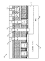
図1は、本開示の一態様によるFinFET構造を示す。FinFET構造100は、基板102と酸化物拡散(OD)の活性領域104とを含む。基板上で、金属−拡散(MD)配線106は、OD104上の第1の導電(たとえば、金属、ポリシリコン、または他の導電)層であり得る。加えて、シャロートレンチ分離(STI)層110上のMD配線108は、FinFET構造100の他の層内のエッチングエリアを介して堆積される。MD配線106および108は、タングステン(W)、銅(Cu)、または他の導電材料であり得る。ポリシリコン構造(PO1)112を、図1に示すように、STI層110上に堆積させることも可能である。MD配線106、108、およびポリシリコン構造112上の電圧を制御することによって、回路が制御される。ビアまたはコンタクト(V0)114は、ポリシリコン構造112およびMD配線106、108へのアクセスを可能にする。
FIG. 1 illustrates a FinFET structure according to one aspect of the present disclosure. The
図2は、本開示の一態様によるキャパシタ構造200を示す。MD配線108は、STI層110上にあり、ポリシリコン構造112とインターリーブされる。第1の導電層202(たとえば、M1)は、ビア/コンタクトV0 114を介してMD配線108に結合される。第1の導電層202は、キャパシタ端子204および206として1つおきの導電層接続を使用して結合され得るか、またはキャパシタ構造200を作成するために所望される任意の形で結合され得る。キャパシタ端子204および206は、キャパシタ構造200の端子である。
FIG. 2 illustrates a
MD配線108間のポリシリコン構造112は、MD配線108によって作成された「プレート」間の誘電材料として、追加の相対的な誘電率(K)を提供する。ポリシリコン構造112の電気的にフローティング状態のポリシリコン構造をその間に備えたMD配線108間の効果的な間隔は、およそ30ナノメートルであり得る。この効果的な間隔は、従来のキャパシタのおよそ半分である。MD配線の重複高さは、およそ70ナノメートルであり得る。この構成では、キャパシタ構造200は、従来のMOMキャパシタのキャパシタンスのおよそ4倍を提供する。ビアV0 114を介して第1の導電層202(たとえば、M1)に結合されたMD配線108は、公差を減少させ、キャパシタ構造200のQ値を増大させるのに役立つ。MD配線108(たとえば、「フィンガー」)間のポリシリコン構造112は、キャパシタ密度を増大させるのに役立ち、作製の間にポリシリコン密度規格を満たすのに役立つ。キャパシタ構造200を、従来のキャパシタなど、他のキャパシタで積層することも可能である。
The
図3は、本開示の別の態様によるキャパシタ構造300を示す。MD配線108は、STI層110上にあり、図2に示すように、ポリシリコン構造112はMD配線108とインターリーブされる。第1の導電層202(たとえば、M1)は、ビア/コンタクトV0 114を介してMD配線108に結合される。ポリシリコン構造112はキャパシタ端子204に結合される。ポリシリコン構造112は、キャパシタ構造の外部に存在し得るMP配線とビアとを介して第1の導電層202に(たとえば、端子導電層M1)に結合され得る。第1の導電層202は、キャパシタ構造200を作成するためにキャパシタ端子206に結合され得る。
FIG. 3 illustrates a
この構造では、ポリシリコン構造112は、このとき、MD配線108により近接し、減少した電圧公差を備えたキャパシタ構造300を形成する。減少した電圧公差が提供されるのは、キャパシタ端子204および206の間の誘導体が単位体積あたりより高い電場を受けるためである。しかしながら、キャパシタ構造300は、本開示の本態様では、所与のキャパシタンス用のエリアを削減させる。この効果的な間隔は、従来のキャパシタの間隔のおよそ1/4である。キャパシタ構造300を、従来のキャパシタで積層することも可能である。キャパシタ構造200および300の一側面に結合されるとして示されるが、キャパシタ端子204および206は、本開示の態様で言及される態様から逸脱せずに、キャパシタ構造200および300内の他の場所に結合されてもよい。
In this structure, the
図4は、本開示の一態様によるキャパシタ構造を作製するための方法400を示すプロセスフロー図である。ブロック402で、半導体基板上にポリシリコン構造を作製する。ポリシリコン構造は、たとえば、図2に示したポリシリコン構造112であり得る。ブロック404で、半導体基板上にMD配線を作製する。MD配線は、たとえば、図2に示したMD配線108であり得る。ポリシリコン構造は、図2に示したMD配線を備えたインターリーブ構成で配設され得る。ブロック406で、MD配線および/またはポリシリコン構造を、図2に示したキャパシタ構造としてインターリーブ構成で選択的に接続する。
FIG. 4 is a process flow diagram illustrating a
本開示のさらなる態様によれば、キャパシタ構造について説明する。一構成では、デバイスは半導体基板上のポリシリコン構造を含む。ポリシリコン構造は、図2に示したポリシリコン構造112であり得る。キャパシタ構造はまた、半導体基板上でM1を酸化物拡散領域に配線するための手段を含む。一構成では、ポリシリコン構造は、配線手段を備えたインターリーブ構成で配設される。この構成では、ポリシリコン構造および/または配線手段は、キャパシタ構造としてインターリーブ構成で選択的に接続される。配線手段は、図2に示したようなMD配線108であり得る。別の態様では、前述の手段は、前述の手段によって具陳された機能を実行するように構成された任意の構成または任意の材料であり得る。
According to a further aspect of the present disclosure, a capacitor structure is described. In one configuration, the device includes a polysilicon structure on a semiconductor substrate. The polysilicon structure may be the
図5は、本開示の一態様が有利に採用され得る例示的なワイヤレス通信システム500を示すブロック図である。説明のために、図5は、3つの遠隔ユニット520、530、および550と、2つの基地局540とを示す。ワイヤレス通信システムは、より多くの遠隔ユニットおよび基地局を有し得ることを理解されよう。遠隔ユニット520、530および550は、ICデバイス525A、525Cおよび525Bを含み、これらは開示するキャパシタを含む。基地局、スイッチングデバイス、ネットワーク機器などの他のデバイスも、開示するキャパシタを含み得ることを認識されよう。図5は、基地局540から遠隔ユニット520、530、および550への順方向リンク信号580、ならびに遠隔ユニット520、530、および550から基地局540への逆方向リンク信号590を示す。
FIG. 5 is a block diagram illustrating an example
図5では、遠隔ユニット520はモバイル電話として示され、遠隔ユニット530はポータブルコンピュータとして示され、遠隔ユニット550は、ワイヤレスローカルループシステムにおける固定位置遠隔ユニットとして示されている。たとえば、遠隔ユニットは、モバイル電話、ハンドヘルドパーソナル通信システム(PCS)ユニット、携帯情報端末などのポータブルデータユニット、GPS対応デバイス、ナビゲーションデバイス、セットトップボックス、音楽プレーヤ、ビデオプレーヤ、エンターテインメントユニット、検針機器などの固定位置データユニット、またはデータもしくはコンピュータ命令を記憶する、もしくは取り出す他のデバイス、あるいはそれらの組合せとすることができる。図5は本開示の態様による遠隔ユニットを示すが、本開示は、これらの示された例示的なユニットに限定されない。本開示の態様は、開示したキャパシタを含む多くのデバイスにおいて、適切に採用され得る。
In FIG. 5,
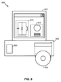
図6は、上記で開示したキャパシタなどの半導体構成要素の回路設計、レイアウト設計、および論理設計に使用される設計用ワークステーションを示すブロック図である。設計用ワークステーション600は、オペレーティングシステムソフトウェア、サポートファイル、およびCadenceやOrCADなどの設計ソフトウェアを収容するハードディスク601を含む。設計用ワークステーション600はまた、回路610の設計または、キャパシタなどの半導体構成要素612の設計を容易にするために、ディスプレイ602を含む。記憶媒体604は、回路610または半導体構成要素612の設計を有形に記憶するために提供される。回路610または半導体構成要素612の設計は、GDSIIまたはGERBERなどのファイルフォーマットにおいて記憶媒体604に記憶され得る。記憶媒体604は、CD−ROM、DVD、ハードディスク、フラッシュメモリ、または他の適切なデバイスであり得る。さらに、設計用ワークステーション600は、記憶媒体604からの入力を受け入れるか、または記憶媒体604への出力を書き込むための駆動装置603を含む。
FIG. 6 is a block diagram illustrating a design workstation used for circuit design, layout design, and logic design of semiconductor components such as capacitors disclosed above. The
記憶媒体604上に記録されるデータは、論理回路構成、フォトリソグラフィマスク用のパターンデータ、または電子ビームリソグラフィなどの連続描画ツール用のマスクパターンデータを指定することができる。データはさらに、論理シミュレーションに関連するタイミングダイアグラムまたはネット回路などの論理検証データをさらに含み得る。記憶媒体604にデータを提供すると、半導体ウエハを設計するためのプロセス数を削減させることによって、回路610または半導体構成要素612の設計が容易になる。
Data recorded on the
本開示のさらなる態様によれば、キャパシタ構造を開示する。一構成では、キャパシタ構造は、半導体基板上に電荷を蓄積するための第1の手段を含む。第1の手段は、ポリシリコン構造112であり得る。キャパシタ構造はまた、半導体基板上に電荷を蓄積するための第2の手段を含む。第2の手段は、MD配線108であり得る。別の態様では、前述の手段は、前述の手段によって具陳された機能を実行するように構成された任意のモジュールまたは任意の装置であり得る。
According to a further aspect of the present disclosure, a capacitor structure is disclosed. In one configuration, the capacitor structure includes first means for storing charge on the semiconductor substrate. The first means may be a
ファームウェアおよび/またはソフトウェアによる実装の場合、本明細書において説明した機能を実行するモジュール(たとえば手続き、関数など)を用いて、方法を実装することができる。本明細書において説明した方法を実装する際に、命令を有形に具現化する機械可読媒体を使用することができる。たとえば、ソフトウェアコードをメモリに記憶させ、プロセッサユニットによって実行することができる。メモリは、プロセッサユニット内またはプロセッサユニットの外部に実装されていてよい。本明細書では、「メモリ」という用語は、長期メモリ、短期メモリ、揮発性メモリ、不揮発性メモリ、または他のメモリのタイプを指し、特定のタイプのメモリもしくは特定の数のメモリ、またはメモリが格納される媒体のタイプに限定すべきではない。 For firmware and / or software implementations, the method may be implemented using modules (eg, procedures, functions, etc.) that perform the functions described herein. In implementing the methods described herein, a machine-readable medium that tangibly embodies instructions can be used. For example, software code can be stored in memory and executed by a processor unit. The memory may be implemented within the processor unit or external to the processor unit. As used herein, the term “memory” refers to a type of long-term memory, short-term memory, volatile memory, non-volatile memory, or other memory, where a particular type of memory or a particular number of memories, or memories It should not be limited to the type of media being stored.
機能は、ファームウェアおよび/またはソフトウェアとして実装する場合、1つもしくは複数の命令またはコードとしてコンピュータ可読媒体上に記憶させることができる。例として、データ構造を符号化したコンピュータ可読媒体、およびコンピュータプログラムを符号化したコンピュータ可読媒体がある。コンピュータ可読媒体は、物理的なコンピュータ記憶媒体を含む。記憶媒体は、コンピュータがアクセスすることのできる利用可能な媒体とすることができる。限定ではなく、例として、そのようなコンピュータ可読媒体は、RAM、ROM、EEPROM、CD−ROMもしくは他の光ディスクストレージ、磁気ディスクストレージもしくは他の磁気記憶デバイス、または、所望のプログラムコードを命令もしくはデータ構造の形で記憶するのに使用することができ、かつコンピュータによってアクセスされ得る他の媒体を含むことができ、本明細書で使用されるディスク(diskおよびdisc)は、コンパクトディスク(disc)(CD)、レーザディスク(disc)、光ディスク(disc)、デジタル多用途ディスク(disc)(DVD)、フロッピーディスク(disk)、およびBlu−ray(登録商標)ディスク(disc)を含み、ディスク(disk)は通常、データを磁気的に再生するが、ディスク(disc)はデータをレーザによって光学的に再生する。上記のものの組合せも、コンピュータ可読媒体の範囲内に含まれるべきである。 The functionality, when implemented as firmware and / or software, can be stored on a computer-readable medium as one or more instructions or code. Examples include computer readable media encoded data structures and computer readable media encoded computer programs. Computer-readable media includes physical computer storage media. A storage media may be any available media that can be accessed by a computer. By way of example, and not limitation, such computer-readable media includes RAM, ROM, EEPROM, CD-ROM or other optical disk storage, magnetic disk storage or other magnetic storage device, or instructions or data for desired program code. Other media that can be used to store in the form of structures and that can be accessed by a computer can be included, and the discs (disk and disc) used herein are compact discs (disc) ( CD, laser disc (disc), optical disc (disc), digital versatile disc (disc) (DVD), floppy disc (disk), and Blu-ray (registered trademark) disc (disc) Is usually data Plays magnetically, disc (while discs) is reproduce data optically with lasers. Combinations of the above should also be included within the scope of computer-readable media.
コンピュータ可読媒体におけるストレージに加えて、命令および/またはデータは、通信装置内に含まれる伝送媒体における信号として提供することができる。たとえば、通信装置は、命令およびデータを示す信号を有するトランシーバを含むことができる。命令およびデータは、1つまたは複数のプロセッサに、特許請求の範囲において概説される機能を実装させるように構成される。 In addition to storage on computer-readable media, instructions and / or data can be provided as signals on transmission media included within the communication device. For example, the communication device can include a transceiver having signals indicative of instructions and data. The instructions and data are configured to cause one or more processors to implement the functions outlined in the claims.
以上、本開示およびその利点について詳細に説明してきたが、添付の特許請求の範囲によって定められる本開示の技術から逸脱することなく、本明細書において様々な変更、置換、および改変を行えることを理解されたい。たとえば、「上」および「下」などの関係性の用語が、基板または電子デバイスに関して使用される。当然、基板または電子デバイスが反転した場合、上は下に、下は上になる。加えて、横向きの場合、上および下は、基板または電子デバイスの側面を指す場合がある。さらに、本出願の範囲は、本明細書で説明したプロセス、機械、製造、組成物、手段、方法、およびステップの特定の構成に限定されることは意図されない。当業者が本開示から容易に諒解するように、本明細書で説明した対応する構成と実質的に同じ機能を実行するか、もしくは実質的に同じ結果を実現する、現存するもしくは今後開発されるプロセス、機械、製造、組成物、手段、方法、またはステップが、本開示に従って利用され得る。したがって、添付の特許請求の範囲は、そのようなプロセス、機械、製造、組成物、手段、方法、またはステップをそれらの範囲内に含むものとする。 Although the present disclosure and its advantages have been described in detail above, various changes, substitutions, and modifications can be made herein without departing from the technology of the present disclosure as defined by the appended claims. I want you to understand. For example, relationship terms such as “above” and “below” are used with respect to a substrate or electronic device. Of course, if the substrate or electronic device is flipped, the top is down and the bottom is up. In addition, when in landscape orientation, top and bottom may refer to the sides of the substrate or electronic device. Furthermore, the scope of the present application is not intended to be limited to the particular configurations of the processes, machines, manufacture, compositions, means, methods, and steps described herein. As those skilled in the art will readily appreciate from this disclosure, existing or future developed that perform substantially the same function or achieve substantially the same results as the corresponding configurations described herein. Any process, machine, manufacture, composition, means, method, or step may be utilized in accordance with the present disclosure. Accordingly, the appended claims are intended to include within their scope such processes, machines, manufacture, compositions of matter, means, methods, or steps.
本明細書で本開示に関連して説明された様々な例示的論理ブロック、モジュール、回路、およびアルゴリズムステップが、電子ハードウェア、コンピュータソフトウェア、または両方の組合せとして実装され得ることを当業者ならさらに理解されよう。ハードウェアとソフトウェアのこの互換性を明確に示すために、様々な例示的構成要素、ブロック、モジュール、回路、およびステップが、上記ではその機能に関して一般的に説明された。そのような機能がハードウェアとして実装されるか、それともソフトウェアとして実装されるかは、特定の応用分野およびシステム全体に対して課される設計制限に依存する。当業者は、説明された機能を各々の特定の応用分野について様々な方式で実装し得るが、そのような実装判断は、本開示の範囲からの逸脱を引き起こすと解釈されるべきではない。 Those skilled in the art will further appreciate that the various exemplary logic blocks, modules, circuits, and algorithm steps described herein in connection with the present disclosure can be implemented as electronic hardware, computer software, or a combination of both. It will be understood. To clearly illustrate this interchangeability of hardware and software, various illustrative components, blocks, modules, circuits, and steps have been described above generally in terms of their functionality. Whether such functionality is implemented as hardware or software depends upon the particular application and design constraints imposed on the overall system. Those skilled in the art may implement the described functionality in a variety of ways for each particular application, but such implementation decisions should not be construed as causing a departure from the scope of the present disclosure.
本明細書の開示に関連して説明した様々な例示的論理ブロック、モジュール、および回路は、本明細書で説明した機能を実施するように設計された汎用プロセッサ、デジタル信号プロセッサ(DSP)、特定用途向け集積回路(ASIC)、フィールドプログラマブルゲートアレイ(FPGA)もしくは他のプログラマブル論理デバイス、ディスクリートゲートもしくはトランジスタロジック、ディスクリートハードウェア構成要素、またはそれらの任意の組合せとともに実装あるいは実施され得る。汎用プロセッサはマイクロプロセッサでよいが、別の方法として、プロセッサは、任意の従来型プロセッサ、コントローラ、マイクロコントローラまたはステートマシンでよい。プロセッサはまた、コンピューティングデバイスの組合せ、たとえば、DSPとマイクロプロセッサとの組合せ、複数のマイクロプロセッサ、DSPコアと連携する1つもしくは複数のマイクロプロセッサ、または任意の他のそのような構成として実装され得る。 Various exemplary logic blocks, modules, and circuits described in connection with the disclosure herein are general purpose processors, digital signal processors (DSPs), specific, designed to perform the functions described herein. It may be implemented or implemented with an application specific integrated circuit (ASIC), a field programmable gate array (FPGA) or other programmable logic device, a discrete gate or transistor logic, a discrete hardware component, or any combination thereof. A general purpose processor may be a microprocessor, but in the alternative, the processor may be any conventional processor, controller, microcontroller, or state machine. The processor is also implemented as a combination of computing devices, eg, a DSP and microprocessor combination, a plurality of microprocessors, one or more microprocessors associated with a DSP core, or any other such configuration. obtain.
本開示に関連して説明した方法またはアルゴリズムのステップは、ハードウェアで直接的に、プロセッサによって実行されるソフトウェアモジュールで、またはその2つの組合せで実施され得る。ソフトウェアモジュールは、RAM、フラッシュメモリ、ROM、EPROM、EEPROM、レジスタ、ハードディスク、リムーバブルディスク、CD−ROM、または当技術分野で知られている任意の他の形態の記憶媒体に常駐することができる。例示的記憶媒体がプロセッサに結合され、プロセッサが記憶媒体から情報を読み取ること、および記憶媒体に情報を書き込むことができるようにする。代替案では、記憶媒体は、プロセッサに一体とされ得る。プロセッサおよび記憶媒体は、ASIC内に存在し得る。ASICは、ユーザ端末内に存在し得る。代替として、プロセッサおよび記憶媒体は、ユーザ端末内にディスクリート構成要素として存在し得る。 The method or algorithm steps described in connection with this disclosure may be implemented directly in hardware, in software modules executed by a processor, or in a combination of the two. A software module may reside in RAM, flash memory, ROM, EPROM, EEPROM, registers, hard disk, removable disk, CD-ROM, or any other form of storage medium known in the art. An exemplary storage medium is coupled to the processor such that the processor can read information from, and write information to, the storage medium. In the alternative, the storage medium may be integral to the processor. The processor and the storage medium may reside in an ASIC. The ASIC may be present in the user terminal. In the alternative, the processor and the storage medium may reside as discrete components in a user terminal.
1つまたは複数の例示的設計では、説明される機能は、ハードウェア、ソフトウェア、ファームウェア、またはそれらの任意の組合せで実装され得る。ソフトウェアで実装される場合、機能は、コンピュータ可読記憶媒体上に1つもしくは複数の命令またはコードとして格納あるいは送信され得る。コンピュータ可読媒体は、コンピュータ記憶媒体と、コンピュータプログラムの1つの場所から別の場所への転送を容易にする任意の媒体を含む通信媒体との両方を含む。記憶媒体は、汎用または特殊用途コンピュータによってアクセスされ得る任意の使用可能な媒体であってもよい。限定ではなく例として、そのようなコンピュータ可読媒体は、RAM、ROM、EEPROM、CD−ROM、もしくは他の光ディスクストレージ、磁気ディスクストレージもしくは他の磁気記憶デバイス、あるいは命令またはデータ構造の形態の規定のプログラムコード手段を搬送もしくは格納するために使用され得、汎用もしくは専用コンピュータ、または汎用もしくは専用プロセッサによってアクセスされ得る任意の他の媒体を含み得る。また、任意の接続が適切にコンピュータ可読媒体と呼ばれる。たとえば、ソフトウェアが、同軸ケーブル、光ファイバケーブル、ツイストペア、デジタル加入者線(「DSL」)、もしくは赤外線、無線、およびマイクロ波などのワイヤレス技術を使用してウェブサイト、サーバ、または他の遠隔ソースから送信される場合、同軸ケーブル、光ファイバケーブル、ツイストペア、DSL、または赤外線、無線、およびマイクロ波などのワイヤレス技術は、媒体の定義に含まれる。本明細書で使用する場合、ディスク(disk)およびディスク(disc)は、コンパクトディスク(disc)(CD)、レーザディスク(disc)、光ディスク(disc)、デジタル多用途ディスク(disc)(DVD)、フロッピーディスク(disk)およびBlu−ray(登録商標)ディスク(disc)を含み、ディスク(disk)は、通常、データを磁気的に再生し、ディスク(disc)は、データをレーザで光学的に再生する。上記のものの組合せも、コンピュータ可読媒体の範囲内に含まれるべきである。 In one or more exemplary designs, the functions described may be implemented in hardware, software, firmware, or any combination thereof. If implemented in software, the functions may be stored on or transmitted over as one or more instructions or code on a computer-readable storage medium. Computer-readable media includes both computer storage media and communication media including any medium that facilitates transfer of a computer program from one place to another. A storage media may be any available media that can be accessed by a general purpose or special purpose computer. By way of example, and not limitation, such computer readable media may be RAM, ROM, EEPROM, CD-ROM, or other optical disk storage, magnetic disk storage or other magnetic storage device, or defined in the form of instructions or data structures. It may be used to carry or store program code means and may include a general purpose or special purpose computer, or any other medium that can be accessed by a general purpose or special purpose processor. Also, any connection is properly termed a computer-readable medium. For example, the software may use a coaxial cable, fiber optic cable, twisted pair, digital subscriber line (“DSL”), or website, server, or other remote source using wireless technologies such as infrared, wireless, and microwave. When transmitting from a coaxial cable, fiber optic cable, twisted pair, DSL, or wireless technologies such as infrared, radio, and microwave are included in the definition of the medium. As used herein, a disc and a disc are a compact disc (disc) (CD), a laser disc (disc), an optical disc (disc), a digital versatile disc (disc), Floppy disk (disk) and Blu-ray (registered trademark) disk (disc) are included, the disk (disk) normally reproduces data magnetically, and the disk (disk) optically reproduces data with a laser. To do. Combinations of the above should also be included within the scope of computer-readable media.
本開示の前述の説明は、いかなる当業者も本開示を作製または使用できるようにするために提供される。本開示に対する様々な修正形態が当業者には容易に明らかとなり、本明細書で定義する一般原理は、本開示の趣旨または範囲から逸脱することなく、他の変形形態に適用され得る。したがって、本開示は、本明細書で説明する例および設計に限定されるものではなく、本明細書で開示する原理および新規の特徴に合致する最も広い範囲を与えられるべきである。 The previous description of the disclosure is provided to enable any person skilled in the art to make or use the disclosure. Various modifications to the present disclosure will be readily apparent to those skilled in the art, and the generic principles defined herein may be applied to other variations without departing from the spirit or scope of the disclosure. Accordingly, the present disclosure is not intended to be limited to the examples and designs described herein, but is to be accorded the widest scope consistent with the principles and novel features disclosed herein.
100 FinFET構造
102 基板
104 活性領域
106 金属−拡散(MD)配線
108 MD配線
110 トレンチ分離(STI)層
112 ポリシリコン構造(PO1)
114 ビアまたはコンタクト(V0)、ビア/コンタクト
200 キャパシタ構造
202 第1の導電層
204 キャパシタターミナル
206 キャパシタターミナル
300 キャパシタ構造
400 方法
500 ワイヤレス通信システム
520 遠隔ユニット
525A ICデバイス
525B ICデバイス
525C ICデバイス
530 遠隔ユニット
540 基地局
550 遠隔ユニット
580 順方向リンク信号
590 逆方向リンク信号
600 設計用ワークステーション
601 ハードディスク
602 ディスプレイ
603 駆動装置
604 記憶媒体
610 回路
612 半導体構成要素
100
114 Via or Contact (V0), Via /
Claims (24)
半導体基板上に複数のポリシリコン構造を作製するステップと、
前記半導体基板上に複数のM1−拡散(MD)配線を作製するステップであって、前記複数のポリシリコン構造が前記複数のMD配線を備えたインターリーブ構成で配設される、作製するステップと、
前記キャパシタ構造として、前記複数のMD配線および/または前記複数のポリシリコン構造の前記インターリーブ構成を選択的に接続するステップと
を含む、方法。 A method for making a capacitor structure comprising:
Creating a plurality of polysilicon structures on a semiconductor substrate;
Producing a plurality of M1-diffusion (MD) wirings on the semiconductor substrate, wherein the plurality of polysilicon structures are arranged in an interleaved configuration comprising the plurality of MD wirings;
Selectively connecting the interleaved configurations of the plurality of MD interconnects and / or the plurality of polysilicon structures as the capacitor structure.
前記半導体基板上の複数のM1−拡散(MD)配線であって、前記複数のポリシリコン構造が、前記複数のMD配線を備えたインターリーブ構成で配設され、前記複数のMD配線および/または前記複数のポリシリコン構造が、キャパシタ構造として前記インターリーブ構成で選択的に接続される、複数のM1−拡散(MD)配線と
を含むキャパシタ構造。 A plurality of polysilicon structures on a semiconductor substrate;
A plurality of M1-diffusion (MD) wirings on the semiconductor substrate, wherein the plurality of polysilicon structures are arranged in an interleaved configuration comprising the plurality of MD wirings; A capacitor structure including a plurality of M1-diffusion (MD) wirings, wherein a plurality of polysilicon structures are selectively connected as a capacitor structure in the interleaved configuration.
半導体基板上に複数のポリシリコン構造を作製するためのステップと、
前記半導体基板上に複数のM1−拡散(MD)配線を作製するためのステップであって、前記複数のポリシリコン構造が前記複数のMD配線を備えたインターリーブ構成で配設される、作製するためのステップと、
前記キャパシタ構造として、前記複数のMD配線および/または前記複数のポリシリコン構造の前記インターリーブ構成を選択的に接続するためのステップと
を含む、方法。 A method for making a capacitor structure comprising:
Steps for producing a plurality of polysilicon structures on a semiconductor substrate;
For producing a plurality of M1-diffusion (MD) wirings on the semiconductor substrate, wherein the plurality of polysilicon structures are arranged in an interleaved configuration with the plurality of MD wirings. And the steps
Selectively connecting the interleaved configurations of the plurality of MD interconnects and / or the plurality of polysilicon structures as the capacitor structure.
前記半導体基板上の酸化物拡散領域に導電層を配線するための手段であって、前記複数のポリシリコン構造が、前記配線手段を備えたインターリーブ構成で配設され、前記複数のポリシリコン構造および/または前記配線手段が、キャパシタ構造として前記インターリーブ構成で選択的に接続される、配線するための手段と
を含むキャパシタ構造。 A plurality of polysilicon structures on a semiconductor substrate;
A means for wiring a conductive layer to an oxide diffusion region on the semiconductor substrate, wherein the plurality of polysilicon structures are arranged in an interleaved configuration including the wiring means, and the plurality of polysilicon structures and And / or means for wiring, wherein the wiring means is selectively connected in the interleave configuration as a capacitor structure.
Applications Claiming Priority (5)
| Application Number | Priority Date | Filing Date | Title |
|---|---|---|---|
| US201361906834P | 2013-11-20 | 2013-11-20 | |
| US61/906,834 | 2013-11-20 | ||
| US14/264,620 | 2014-04-29 | ||
| US14/264,620 US20150137201A1 (en) | 2013-11-20 | 2014-04-29 | High density linear capacitor |
| PCT/US2014/057017 WO2015076926A1 (en) | 2013-11-20 | 2014-09-23 | High density linear capacitor |
Publications (2)
| Publication Number | Publication Date |
|---|---|
| JP2017502496A true JP2017502496A (en) | 2017-01-19 |
| JP2017502496A5 JP2017502496A5 (en) | 2017-10-19 |
Family
ID=53172403
Family Applications (1)
| Application Number | Title | Priority Date | Filing Date |
|---|---|---|---|
| JP2016527204A Pending JP2017502496A (en) | 2013-11-20 | 2014-09-23 | High density linear capacitor |
Country Status (5)
| Country | Link |
|---|---|
| US (1) | US20150137201A1 (en) |
| EP (1) | EP3072170A1 (en) |
| JP (1) | JP2017502496A (en) |
| CN (1) | CN105723535A (en) |
| WO (1) | WO2015076926A1 (en) |
Families Citing this family (4)
| Publication number | Priority date | Publication date | Assignee | Title |
|---|---|---|---|---|
| US10573674B2 (en) | 2018-07-19 | 2020-02-25 | Psemi Corporation | SLT integrated circuit capacitor structure and methods |
| US10658386B2 (en) | 2018-07-19 | 2020-05-19 | Psemi Corporation | Thermal extraction of single layer transfer integrated circuits |
| KR20200116765A (en) | 2019-04-02 | 2020-10-13 | 삼성전자주식회사 | Vertical Capacitor Structure, and Non-volatile memory device including the same |
| US20240055346A1 (en) * | 2022-08-15 | 2024-02-15 | Qualcomm Incorporated | Layout design of custom stack capacitor to procure high capacitance |
Citations (4)
| Publication number | Priority date | Publication date | Assignee | Title |
|---|---|---|---|---|
| JP2001085630A (en) * | 1999-07-14 | 2001-03-30 | Matsushita Electric Ind Co Ltd | Semiconductor device and fabrication method thereof |
| JP2010118563A (en) * | 2008-11-14 | 2010-05-27 | Renesas Technology Corp | Semiconductor device |
| JP2011029249A (en) * | 2009-07-22 | 2011-02-10 | Renesas Electronics Corp | Semiconductor device |
| JP2013183085A (en) * | 2012-03-02 | 2013-09-12 | Toshiba Corp | Method for manufacturing semiconductor device |
Family Cites Families (24)
| Publication number | Priority date | Publication date | Assignee | Title |
|---|---|---|---|---|
| US5208725A (en) * | 1992-08-19 | 1993-05-04 | Akcasu Osman E | High capacitance structure in a semiconductor device |
| US5583359A (en) * | 1995-03-03 | 1996-12-10 | Northern Telecom Limited | Capacitor structure for an integrated circuit |
| US6747307B1 (en) * | 2000-04-04 | 2004-06-08 | Koninklijke Philips Electronics N.V. | Combined transistor-capacitor structure in deep sub-micron CMOS for power amplifiers |
| JP2002217304A (en) * | 2000-11-17 | 2002-08-02 | Rohm Co Ltd | Semiconductor device |
| US6819542B2 (en) * | 2003-03-04 | 2004-11-16 | Taiwan Semiconductor Manufacturing Co., Ltd. | Interdigitated capacitor structure for an integrated circuit |
| JP4525965B2 (en) * | 2004-01-06 | 2010-08-18 | ルネサスエレクトロニクス株式会社 | Semiconductor device |
| US7561407B1 (en) * | 2005-11-28 | 2009-07-14 | Altera Corporation | Multi-segment capacitor |
| JP4908006B2 (en) * | 2006-02-03 | 2012-04-04 | 株式会社東芝 | Semiconductor device |
| TW200847404A (en) * | 2007-05-18 | 2008-12-01 | Nanya Technology Corp | Flash memory device and method for fabricating thereof |
| JP4455621B2 (en) * | 2007-07-17 | 2010-04-21 | 株式会社東芝 | Aging device |
| US8022458B2 (en) * | 2007-10-08 | 2011-09-20 | Taiwan Semiconductor Manufacturing Company, Ltd. | Capacitors integrated with metal gate formation |
| US20090096003A1 (en) * | 2007-10-11 | 2009-04-16 | International Business Machines Corporation | Semiconductor cell structure including buried capacitor and method for fabrication thereof |
| US8120086B2 (en) * | 2008-09-30 | 2012-02-21 | Taiwan Semiconductor Manufacturing Co., Ltd | Low leakage capacitors including portions in inter-layer dielectrics |
| US7994610B1 (en) * | 2008-11-21 | 2011-08-09 | Xilinx, Inc. | Integrated capacitor with tartan cross section |
| JP2010135572A (en) * | 2008-12-05 | 2010-06-17 | Renesas Electronics Corp | Semiconductor device |
| US8237243B2 (en) * | 2009-03-18 | 2012-08-07 | International Business Machines Corporation | On-chip capacitors with a variable capacitance for a radiofrequency integrated circuit |
| US8681459B2 (en) * | 2009-03-31 | 2014-03-25 | Freescale Semiconductor, Inc. | Integrated protection circuit |
| JP2010153905A (en) * | 2010-03-05 | 2010-07-08 | Renesas Technology Corp | Semiconductor device |
| US8420476B2 (en) * | 2010-05-27 | 2013-04-16 | International Business Machines Corporation | Integrated circuit with finFETs and MIM fin capacitor |
| US8860107B2 (en) * | 2010-06-03 | 2014-10-14 | International Business Machines Corporation | FinFET-compatible metal-insulator-metal capacitor |
| US8860148B2 (en) * | 2012-04-11 | 2014-10-14 | Taiwan Semiconductor Manufacturing Company, Ltd. | Structure and method for FinFET integrated with capacitor |
| US8841185B2 (en) * | 2012-08-13 | 2014-09-23 | International Business Machines Corporation | High density bulk fin capacitor |
| KR20150010353A (en) * | 2013-07-19 | 2015-01-28 | 삼성전자주식회사 | A capacitor structure |
| US9685433B2 (en) * | 2013-09-25 | 2017-06-20 | Taiwan Semiconductor Manufacturing Company Ltd. | Capacitor device |
-
2014
- 2014-04-29 US US14/264,620 patent/US20150137201A1/en not_active Abandoned
- 2014-09-23 CN CN201480063001.9A patent/CN105723535A/en active Pending
- 2014-09-23 JP JP2016527204A patent/JP2017502496A/en active Pending
- 2014-09-23 EP EP14780735.8A patent/EP3072170A1/en not_active Ceased
- 2014-09-23 WO PCT/US2014/057017 patent/WO2015076926A1/en active Application Filing
Patent Citations (4)
| Publication number | Priority date | Publication date | Assignee | Title |
|---|---|---|---|---|
| JP2001085630A (en) * | 1999-07-14 | 2001-03-30 | Matsushita Electric Ind Co Ltd | Semiconductor device and fabrication method thereof |
| JP2010118563A (en) * | 2008-11-14 | 2010-05-27 | Renesas Technology Corp | Semiconductor device |
| JP2011029249A (en) * | 2009-07-22 | 2011-02-10 | Renesas Electronics Corp | Semiconductor device |
| JP2013183085A (en) * | 2012-03-02 | 2013-09-12 | Toshiba Corp | Method for manufacturing semiconductor device |
Also Published As
| Publication number | Publication date |
|---|---|
| US20150137201A1 (en) | 2015-05-21 |
| CN105723535A (en) | 2016-06-29 |
| WO2015076926A1 (en) | 2015-05-28 |
| EP3072170A1 (en) | 2016-09-28 |
Similar Documents
| Publication | Publication Date | Title |
|---|---|---|
| US10643985B2 (en) | Capacitor array overlapped by on-chip inductor/transformer | |
| US9252104B2 (en) | Complementary back end of line (BEOL) capacitor | |
| JP6105175B1 (en) | Directional FinFET capacitor structure | |
| KR102164669B1 (en) | On-chip coupling capacitor with patterned radio frequency shielding structure for reducing loss | |
| US10686031B2 (en) | Finger metal-oxide-metal (FMOM) capacitor | |
| US10269490B2 (en) | Metal-oxide-metal capacitor using vias within sets of interdigitated fingers | |
| JP2017502496A (en) | High density linear capacitor | |
| WO2019164598A1 (en) | Folded metal-oxide-metal capacitor overlapped by on-chip inductor/transformer | |
| US10446898B2 (en) | On-chip coplanar waveguide having a shielding layer comprising a capacitor formed by sets of interdigitated fingers | |
| JP6224844B2 (en) | Conductive layer routing | |
| US10651268B2 (en) | Metal-oxide-metal capacitor with improved alignment and reduced capacitance variance | |
| US10615113B2 (en) | Rotated metal-oxide-metal (RTMOM) capacitor | |
| JP2017516305A (en) | Via material selection and processing | |
| TW202147652A (en) | Back-end-of-line (beol) sidewall metal-insulator-metal (mim) capacitor | |
| US9818817B2 (en) | Metal-insulator-metal capacitor over conductive layer | |
| US9478490B2 (en) | Capacitor from second level middle-of-line layer in combination with decoupling capacitors | |
| BR112019026551B1 (en) | CAPACITOR RADIO FREQUENCY (RF) SHIELDING STRUCTURE AND METHOD FOR MANUFACTURING A CAPACITOR RADIO FREQUENCY SHIELDING STRUCTURE |
Legal Events
| Date | Code | Title | Description |
|---|---|---|---|
| A521 | Request for written amendment filed |
Free format text: JAPANESE INTERMEDIATE CODE: A523 Effective date: 20170905 |
|
| A621 | Written request for application examination |
Free format text: JAPANESE INTERMEDIATE CODE: A621 Effective date: 20170905 |
|
| A977 | Report on retrieval |
Free format text: JAPANESE INTERMEDIATE CODE: A971007 Effective date: 20180822 |
|
| A131 | Notification of reasons for refusal |
Free format text: JAPANESE INTERMEDIATE CODE: A131 Effective date: 20180903 |
|
| A02 | Decision of refusal |
Free format text: JAPANESE INTERMEDIATE CODE: A02 Effective date: 20190325 |