JP2017516305A - Via material selection and processing - Google Patents
Via material selection and processing Download PDFInfo
- Publication number
- JP2017516305A JP2017516305A JP2016565680A JP2016565680A JP2017516305A JP 2017516305 A JP2017516305 A JP 2017516305A JP 2016565680 A JP2016565680 A JP 2016565680A JP 2016565680 A JP2016565680 A JP 2016565680A JP 2017516305 A JP2017516305 A JP 2017516305A
- Authority
- JP
- Japan
- Prior art keywords
- conductive material
- interconnect
- interconnect layer
- mol
- conductive
- Prior art date
- Legal status (The legal status is an assumption and is not a legal conclusion. Google has not performed a legal analysis and makes no representation as to the accuracy of the status listed.)
- Pending
Links
Images


Classifications
-
- H—ELECTRICITY
- H01—ELECTRIC ELEMENTS
- H01L—SEMICONDUCTOR DEVICES NOT COVERED BY CLASS H10
- H01L23/00—Details of semiconductor or other solid state devices
- H01L23/52—Arrangements for conducting electric current within the device in operation from one component to another, i.e. interconnections, e.g. wires, lead frames
- H01L23/522—Arrangements for conducting electric current within the device in operation from one component to another, i.e. interconnections, e.g. wires, lead frames including external interconnections consisting of a multilayer structure of conductive and insulating layers inseparably formed on the semiconductor body
- H01L23/5226—Via connections in a multilevel interconnection structure
-
- H—ELECTRICITY
- H01—ELECTRIC ELEMENTS
- H01L—SEMICONDUCTOR DEVICES NOT COVERED BY CLASS H10
- H01L21/00—Processes or apparatus adapted for the manufacture or treatment of semiconductor or solid state devices or of parts thereof
- H01L21/70—Manufacture or treatment of devices consisting of a plurality of solid state components formed in or on a common substrate or of parts thereof; Manufacture of integrated circuit devices or of parts thereof
- H01L21/71—Manufacture of specific parts of devices defined in group H01L21/70
- H01L21/768—Applying interconnections to be used for carrying current between separate components within a device comprising conductors and dielectrics
- H01L21/76801—Applying interconnections to be used for carrying current between separate components within a device comprising conductors and dielectrics characterised by the formation and the after-treatment of the dielectrics, e.g. smoothing
- H01L21/76802—Applying interconnections to be used for carrying current between separate components within a device comprising conductors and dielectrics characterised by the formation and the after-treatment of the dielectrics, e.g. smoothing by forming openings in dielectrics
- H01L21/76807—Applying interconnections to be used for carrying current between separate components within a device comprising conductors and dielectrics characterised by the formation and the after-treatment of the dielectrics, e.g. smoothing by forming openings in dielectrics for dual damascene structures
- H01L21/76811—Applying interconnections to be used for carrying current between separate components within a device comprising conductors and dielectrics characterised by the formation and the after-treatment of the dielectrics, e.g. smoothing by forming openings in dielectrics for dual damascene structures involving multiple stacked pre-patterned masks
-
- H—ELECTRICITY
- H01—ELECTRIC ELEMENTS
- H01L—SEMICONDUCTOR DEVICES NOT COVERED BY CLASS H10
- H01L21/00—Processes or apparatus adapted for the manufacture or treatment of semiconductor or solid state devices or of parts thereof
- H01L21/70—Manufacture or treatment of devices consisting of a plurality of solid state components formed in or on a common substrate or of parts thereof; Manufacture of integrated circuit devices or of parts thereof
- H01L21/71—Manufacture of specific parts of devices defined in group H01L21/70
- H01L21/768—Applying interconnections to be used for carrying current between separate components within a device comprising conductors and dielectrics
- H01L21/76801—Applying interconnections to be used for carrying current between separate components within a device comprising conductors and dielectrics characterised by the formation and the after-treatment of the dielectrics, e.g. smoothing
- H01L21/76802—Applying interconnections to be used for carrying current between separate components within a device comprising conductors and dielectrics characterised by the formation and the after-treatment of the dielectrics, e.g. smoothing by forming openings in dielectrics
- H01L21/76816—Aspects relating to the layout of the pattern or to the size of vias or trenches
-
- H—ELECTRICITY
- H01—ELECTRIC ELEMENTS
- H01L—SEMICONDUCTOR DEVICES NOT COVERED BY CLASS H10
- H01L21/00—Processes or apparatus adapted for the manufacture or treatment of semiconductor or solid state devices or of parts thereof
- H01L21/70—Manufacture or treatment of devices consisting of a plurality of solid state components formed in or on a common substrate or of parts thereof; Manufacture of integrated circuit devices or of parts thereof
- H01L21/71—Manufacture of specific parts of devices defined in group H01L21/70
- H01L21/768—Applying interconnections to be used for carrying current between separate components within a device comprising conductors and dielectrics
- H01L21/76838—Applying interconnections to be used for carrying current between separate components within a device comprising conductors and dielectrics characterised by the formation and the after-treatment of the conductors
- H01L21/76877—Filling of holes, grooves or trenches, e.g. vias, with conductive material
- H01L21/76879—Filling of holes, grooves or trenches, e.g. vias, with conductive material by selective deposition of conductive material in the vias, e.g. selective C.V.D. on semiconductor material, plating
-
- H—ELECTRICITY
- H01—ELECTRIC ELEMENTS
- H01L—SEMICONDUCTOR DEVICES NOT COVERED BY CLASS H10
- H01L23/00—Details of semiconductor or other solid state devices
- H01L23/52—Arrangements for conducting electric current within the device in operation from one component to another, i.e. interconnections, e.g. wires, lead frames
- H01L23/522—Arrangements for conducting electric current within the device in operation from one component to another, i.e. interconnections, e.g. wires, lead frames including external interconnections consisting of a multilayer structure of conductive and insulating layers inseparably formed on the semiconductor body
- H01L23/5228—Resistive arrangements or effects of, or between, wiring layers
-
- H—ELECTRICITY
- H01—ELECTRIC ELEMENTS
- H01L—SEMICONDUCTOR DEVICES NOT COVERED BY CLASS H10
- H01L23/00—Details of semiconductor or other solid state devices
- H01L23/52—Arrangements for conducting electric current within the device in operation from one component to another, i.e. interconnections, e.g. wires, lead frames
- H01L23/522—Arrangements for conducting electric current within the device in operation from one component to another, i.e. interconnections, e.g. wires, lead frames including external interconnections consisting of a multilayer structure of conductive and insulating layers inseparably formed on the semiconductor body
- H01L23/532—Arrangements for conducting electric current within the device in operation from one component to another, i.e. interconnections, e.g. wires, lead frames including external interconnections consisting of a multilayer structure of conductive and insulating layers inseparably formed on the semiconductor body characterised by the materials
- H01L23/5329—Insulating materials
- H01L23/53295—Stacked insulating layers
-
- H—ELECTRICITY
- H01—ELECTRIC ELEMENTS
- H01L—SEMICONDUCTOR DEVICES NOT COVERED BY CLASS H10
- H01L23/00—Details of semiconductor or other solid state devices
- H01L23/52—Arrangements for conducting electric current within the device in operation from one component to another, i.e. interconnections, e.g. wires, lead frames
- H01L23/522—Arrangements for conducting electric current within the device in operation from one component to another, i.e. interconnections, e.g. wires, lead frames including external interconnections consisting of a multilayer structure of conductive and insulating layers inseparably formed on the semiconductor body
- H01L23/532—Arrangements for conducting electric current within the device in operation from one component to another, i.e. interconnections, e.g. wires, lead frames including external interconnections consisting of a multilayer structure of conductive and insulating layers inseparably formed on the semiconductor body characterised by the materials
- H01L23/53204—Conductive materials
- H01L23/53209—Conductive materials based on metals, e.g. alloys, metal silicides
- H01L23/53228—Conductive materials based on metals, e.g. alloys, metal silicides the principal metal being copper
-
- H—ELECTRICITY
- H01—ELECTRIC ELEMENTS
- H01L—SEMICONDUCTOR DEVICES NOT COVERED BY CLASS H10
- H01L23/00—Details of semiconductor or other solid state devices
- H01L23/52—Arrangements for conducting electric current within the device in operation from one component to another, i.e. interconnections, e.g. wires, lead frames
- H01L23/522—Arrangements for conducting electric current within the device in operation from one component to another, i.e. interconnections, e.g. wires, lead frames including external interconnections consisting of a multilayer structure of conductive and insulating layers inseparably formed on the semiconductor body
- H01L23/532—Arrangements for conducting electric current within the device in operation from one component to another, i.e. interconnections, e.g. wires, lead frames including external interconnections consisting of a multilayer structure of conductive and insulating layers inseparably formed on the semiconductor body characterised by the materials
- H01L23/53204—Conductive materials
- H01L23/53209—Conductive materials based on metals, e.g. alloys, metal silicides
- H01L23/53257—Conductive materials based on metals, e.g. alloys, metal silicides the principal metal being a refractory metal
-
- H—ELECTRICITY
- H01—ELECTRIC ELEMENTS
- H01L—SEMICONDUCTOR DEVICES NOT COVERED BY CLASS H10
- H01L2924/00—Indexing scheme for arrangements or methods for connecting or disconnecting semiconductor or solid-state bodies as covered by H01L24/00
- H01L2924/0001—Technical content checked by a classifier
- H01L2924/0002—Not covered by any one of groups H01L24/00, H01L24/00 and H01L2224/00
Abstract
半導体インターコネクトおよび半導体インターコネクトを形成するための方法。インターコネクトが、第1の導電性インターコネクト層と第1のミドルオブライン(MOL)インターコネクト層との間の第1の導電性材料の第1のビアを含むことができる。第1のMOLインターコネクト層は第1のレベルにある。第1のビアはシングルダマシンプロセスで製造される。そのような半導体インターコネクトは、第1の導電性インターコネクト層と第2のMOLインターコネクト層との間の第2の導電性材料の第2のビアも含む。第2のMOLインターコネクト層は第2のレベルにある。第2のビアはデュアルダマシンプロセスで製造される。第1の導電性材料は第2の導電性材料とは異なる。A semiconductor interconnect and a method for forming a semiconductor interconnect. The interconnect can include a first via of a first conductive material between the first conductive interconnect layer and the first middle-of-line (MOL) interconnect layer. The first MOL interconnect layer is at the first level. The first via is manufactured by a single damascene process. Such a semiconductor interconnect also includes a second via of a second conductive material between the first conductive interconnect layer and the second MOL interconnect layer. The second MOL interconnect layer is at the second level. The second via is manufactured by a dual damascene process. The first conductive material is different from the second conductive material.
Description
本開示の態様は半導体デバイスに関し、より詳細には、集積回路内の、ミドルオブライン層のような配線用導電層に関する。 Aspects of the present disclosure relate to semiconductor devices, and more particularly to a conductive layer for wiring, such as a middle-of-line layer, in an integrated circuit.
半導体製造プロセスは、しばしば、3つの部分、すなわち、フロントエンドオブライン(FEOL:front end of line)、ミドルオブライン(MOL:middle of line)、およびバックエンドオブラインに分割される(BEOL:back end of line)。フロントエンドオブラインプロセスは、ウェハ準備、絶縁、ウェル形成、ゲートパターニング、スペーサ、およびドーパント注入を含む。ミドルオブラインプロセスは、ゲート形成および端子コンタクト形成を含む。バックエンドオブラインプロセスは、FEOLデバイスに結合するためのインターコネクトおよび誘電体層を形成することを含む。 The semiconductor manufacturing process is often divided into three parts: a front end of line (FEOL), a middle of line (MOL), and a back end of line (BEOL: back end of line). line). The front end of line process includes wafer preparation, insulation, well formation, gate patterning, spacers, and dopant implantation. The middle-of-line process includes gate formation and terminal contact formation. The back-end of line process includes forming interconnects and dielectric layers for coupling to FEOL devices.
これらのインターコネクトは、プラズマ化学気相成長(PECVD)堆積層間誘電体(ILD:interlayer dielectric)材料を使用するデュアルダマシンプロセスを用いて製造することができる。半導体回路のこれらのインターコネクト層は、チップ設計の密度が高くなったため、より小さくなり、配線するのがより難しくなってきた。種々のインターコネクト層を接続するために使用されるいくつかの材料は、より高い抵抗を有するので、これが、これらの「ビア」または電気経路のタイミングおよび/または抵抗特性に影響を及ぼす場合がある。一例として、層間のビアのために、しばしばタングステンが使用される。ビアの深さと直径との比は、アスペクト比と呼ばれる。タングステンは、タングステン材料をビア内に堆積するか、または別の方法で結合するために、「シングルダマシン」(SD)プロセスにおいてしばしば処理される。銅はしばしば「デュアルダマシン」(DD)プロセスにおいて処理される。 These interconnects can be fabricated using a dual damascene process using plasma enhanced chemical vapor deposition (PECVD) deposited interlayer dielectric (ILD) materials. These interconnect layers of semiconductor circuits have become smaller and more difficult to route due to the increased chip design density. Because some materials used to connect the various interconnect layers have higher resistance, this may affect the timing and / or resistance characteristics of these “vias” or electrical paths. As an example, tungsten is often used for interlayer vias. The ratio between the depth and diameter of the via is called the aspect ratio. Tungsten is often processed in a “single damascene” (SD) process in order to deposit or otherwise bond tungsten material in vias. Copper is often processed in a “dual damascene” (DD) process.
半導体インターコネクトが、第1の導電性インターコネクト層と第1のミドルオブライン(MOL)インターコネクト層との間に第1の導電性材料の第1のビアを含むことができる。第1のMOLインターコネクト層は第1のレベルにある。第1のビアはシングルダマシンプロセスで製造される。そのような半導体インターコネクトは、第1の導電性インターコネクト層と第2のMOLインターコネクト層との間に第2の導電性材料の第2のビアも含む。第2のMOLインターコネクト層は第2のレベルにある。第2のビアはデュアルダマシンプロセスで製造される。第1の導電性材料は第2の導電性材料とは異なる。 The semiconductor interconnect can include a first via of a first conductive material between the first conductive interconnect layer and the first middle-of-line (MOL) interconnect layer. The first MOL interconnect layer is at the first level. The first via is manufactured by a single damascene process. Such a semiconductor interconnect also includes a second via of a second conductive material between the first conductive interconnect layer and the second MOL interconnect layer. The second MOL interconnect layer is at the second level. The second via is manufactured by a dual damascene process. The first conductive material is different from the second conductive material.
ミドルオブライン(MOL)インターコネクトを製造するための方法が、第1の導電性材料の第1のビアを製造することを含むことができる。第1のビアは第1のレベルにある第1のMOLインターコネクト層に結合される。第1のビアはシングルダマシンプロセスで形成される。また、その方法は、第2の導電性材料の第2のビアおよび第1の導電性インターコネクト層を製造することも含む。第2のビアはデュアルダマシンプロセスで形成される。第1の導電性インターコネクト層は第1のビアに結合する。第1の導電性材料は第2の導電性材料とは異なる。第2のビアは第2のレベルにある第2のMOLインターコネクト層に結合される。 A method for manufacturing a middle-of-line (MOL) interconnect can include manufacturing a first via of a first conductive material. The first via is coupled to the first MOL interconnect layer at the first level. The first via is formed by a single damascene process. The method also includes fabricating a second via of the second conductive material and a first conductive interconnect layer. The second via is formed by a dual damascene process. The first conductive interconnect layer is coupled to the first via. The first conductive material is different from the second conductive material. The second via is coupled to the second MOL interconnect layer at the second level.
半導体インターコネクトが、第1の導電性インターコネクト層と第1のミドルオブライン(MOL)インターコネクト層との間の電流を伝導させるための手段を含むことができる。第1のMOLインターコネクト層は第1のレベルにある。第1の手段は、シングルダマシンプロセスにおいて第1の導電性材料で製造される。また、インターコネクトは、第1の導電性インターコネクト層と少なくとも第2のMOLインターコネクト層との間の電流を伝導させるための手段も含む。第2のMOLインターコネクト層は第2のレベルにある。第2の手段は、デュアルダマシンプロセスにおいて第2の導電性材料で製造される。第1の導電性材料は第2の導電性材料とは異なる。 The semiconductor interconnect can include means for conducting current between the first conductive interconnect layer and the first middle-of-line (MOL) interconnect layer. The first MOL interconnect layer is at the first level. The first means is made of the first conductive material in a single damascene process. The interconnect also includes means for conducting current between the first conductive interconnect layer and at least the second MOL interconnect layer. The second MOL interconnect layer is at the second level. The second means is made of the second conductive material in a dual damascene process. The first conductive material is different from the second conductive material.
上記では、後続の詳細な説明をより深く理解することができるように、本開示の特徴および技術的利点について、かなり大まかに概説してきた。本開示の追加の特徴および利点が、以下で説明されることになる。本開示が、本開示と同じ目的を果たすための他の構造を変更または設計するための基礎として容易に利用できることを、当業者は理解されたい。そのような同等な構成が、添付の特許請求の範囲に記載されるような本開示の教示から逸脱しないことも、当業者には理解されたい。本開示の構成と動作方法の両方に関して本開示の特徴になると考えられる新規の特徴が、さらなる目的および利点とともに、以下の説明を添付の図と併せて検討することからより十分に理解されるであろう。しかしながら、図の各々が、例示および説明のために提供されるにすぎず、本開示の範囲を定めるものではないことは明確に理解されたい。 The foregoing has outlined rather broadly the features and technical advantages of the present disclosure in order that the detailed description that follows may be better understood. Additional features and advantages of the present disclosure will be described below. Those skilled in the art will appreciate that the present disclosure can be readily utilized as a basis for modifying or designing other structures to serve the same purpose as the present disclosure. It should also be understood by those skilled in the art that such equivalent constructions do not depart from the teachings of the present disclosure as set forth in the appended claims. The novel features believed to be features of this disclosure in terms of both the structure and method of operation of this disclosure, together with further objects and advantages, will be more fully understood from a consideration of the following description in conjunction with the accompanying figures. I will. However, it should be clearly understood that each of the figures is provided for purposes of illustration and description only and does not delimit the scope of the present disclosure.
本開示をより完全に理解してもらうために、ここで、添付の図面とともに取り上げられる以下の説明が参照される。 For a more complete understanding of the present disclosure, reference is now made to the following description, taken in conjunction with the accompanying drawings, in which:
添付の図面との関連で以下に記載される詳細な説明は、種々の構成を説明することを意図しており、本明細書において説明される概念を実践できる唯一の構成を表すことは意図していない。詳細な説明は、種々の概念を完全に理解してもらうことを目的とした具体的な詳細を含む。しかしながら、これらの概念がこれらの具体的な詳細なしに実施できることは当業者には明らかであろう。場合によっては、そのような概念を曖昧にするのを避けるために、よく知られている構造および構成要素がブロック図の形で示される。本明細書において説明されるときに、「および/または」という用語の使用は、「包含的論理和」を表すことが意図されており、「または」という用語の使用は、「排他的論理和」を表すことが意図されている。 The detailed description set forth below in connection with the accompanying drawings is intended to illustrate various configurations and is not intended to represent the only configurations capable of practicing the concepts described herein. Not. The detailed description includes specific details that are intended to provide a thorough understanding of various concepts. However, it will be apparent to those skilled in the art that these concepts can be practiced without these specific details. In some instances, well-known structures and components are shown in block diagram form in order to avoid obscuring such concepts. As used herein, the use of the term “and / or” is intended to represent “inclusive or”, and the use of the term “or” is “exclusive or”. Is intended to represent.
本開示の種々の態様は、集積回路内のミドルオブライン層のような配線用導電層のための技法を提供する。集積回路の半導体製造のためのプロセスフローは、フロントエンドオブライン(FEOL)プロセス、ミドルオブライン(MOL)プロセス、およびバックエンドオブライン(BEOL)プロセスを含むことができる。「層」という用語は、膜を含み、別段述べられていない限り、垂直厚または水平厚を示すものと解釈されるべきではないことは理解されよう。本明細書において説明されるように、「半導体基板」という用語は、ダイシングされたウェハの基板を指す場合があるか、または、ダイシングされていないウェハの基板を指す場合がある。同様に、ウェハおよびダイという用語は、入れ換えられると信じることが難しくない限り、互換的に使用することができる。 Various aspects of the present disclosure provide techniques for wiring conductive layers, such as middle-of-line layers in integrated circuits. Process flows for integrated circuit semiconductor manufacturing can include front-end-of-line (FEOL), middle-of-line (MOL), and back-end-of-line (BEOL) processes. It will be understood that the term “layer” includes a membrane and should not be construed to indicate a vertical or horizontal thickness unless otherwise stated. As described herein, the term “semiconductor substrate” may refer to a substrate of a diced wafer or may refer to a substrate of an undiced wafer. Similarly, the terms wafer and die can be used interchangeably unless it is difficult to believe that they will be interchanged.
本開示の一態様によれば、ハイブリッドビア構造、およびハイブリッドビア構造を形成するプロセスが説明される。1つの構成では、半導体デバイスのいくつかのインターコネクト層のためのシングルダマシンプロセスを用いて、第1の材料が、第1のインターコネクト層に結合される。他のインターコネクト層の場合、デュアルダマシンプロセスが、第2の材料を第2のインターコネクト層に結合する。第2の材料は第1の材料に結合される場合もある。本開示のこの態様は、相互接続のうちのいくつかの相互接続の抵抗を下げ、回路の全体性能を高めることができる。導電層は、半導体デバイス内の第1の導電層(たとえば、金属1(M1))とすることもできる。 According to one aspect of the present disclosure, a hybrid via structure and a process for forming a hybrid via structure are described. In one configuration, the first material is coupled to the first interconnect layer using a single damascene process for several interconnect layers of the semiconductor device. For other interconnect layers, a dual damascene process couples the second material to the second interconnect layer. The second material may be bonded to the first material. This aspect of the present disclosure can reduce the resistance of some of the interconnects and increase the overall performance of the circuit. The conductive layer can also be a first conductive layer (eg, metal 1 (M1)) in the semiconductor device.
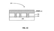
半導体デバイス内の導電層間の接続は、「ビア」とも呼ばれ、半導体チップのデバイス間またはエリア間で信号を転送するために使用される。これらの経路は多くの場合に、ダマシンプロセスを用いて作製される。「シングルダマシン」(SD)プロセスが図1A〜図1Eに示される。 Connections between conductive layers in semiconductor devices, also called “vias”, are used to transfer signals between devices or areas of a semiconductor chip. These paths are often made using a damascene process. A “single damascene” (SD) process is illustrated in FIGS. 1A-1E.
図1Aは、基板102と、エッチストップ層104と、誘電体層106と、フォトレジスト層108とを有するウェハ100を示す。ウェハ100は、本開示の範囲から逸脱することなく、ダイ、チップまたは他のデバイスとすることができる。誘電体層106は、本開示の範囲から逸脱することなく、酸化シリコンのような酸化物、または他の絶縁材料とすることができる。
FIG. 1A shows a
図1Bに示されるように、フォトレジスト層108は選択的にパターニングされ、誘電体層106内に開口部110、112および114が形成される。開口部110〜114の深さ116は、誘電体層106の厚さに基づく。開口部110の幅118は、開口部114の幅120とは異なる場合がある。開口部の幅と深さとの比は、開口部110〜114の「アスペクト比」と呼ばれる。誘電体層106は、ウェット化学エッチング、プラズマエッチングまたは他の誘電体材料除去技法を用いてエッチングすることができる。所望により、エッチストップ層104も除去される場合がある。
As shown in FIG. 1B, the
図1Cにおいて、ダイ100に導電層122が加えられる。導電層122は、誘電体層106の露出した部分の上だけでなく、開口部110〜114内にも堆積される。その場合に、基板102は、開口部110〜114を通して導電層122に電気的に、および/または機械的に結合される。導電層は、開口部110〜114が導電層122の材料で実質的に満たされるように、電着または電気めっきプロセスを用いて堆積することができるか、またはスパッタリングすることができるか、もしくは別の方法でダイ100に結合することができる。導電層122が堆積されると、開口部110〜114は「ビア」または「相互接続経路」と呼ばれる場合がある。
In FIG. 1C, a
導電層122は、開口部110〜114および誘電体層106の表面を覆う障壁層を含むことができる。障壁層の部分は、タンタル、窒化タンタル、窒化チタン、チタン−タングステン、または他の材料とすることができる。導電層122の障壁層部分は、導電層から誘電体層106および/または基板102への材料の拡散を低減する。導電層122は、開口部110〜114内の導電層122と基板102との間の機械的および/または電気的結合を助けるシード層を含むこともできる。
The
図1Dにおいて、導電層122および誘電体層106が平坦になるように、導電層122の一部が除去される。このプロセスは、化学機械平坦化(CMP:chemical mechanical planarization)と呼ばれる場合があるが、本開示の範囲から逸脱することなく、他の技法を用いて平坦化を実行することもできる。図1Eは、導電層122を封入する、ダイ100上の別の誘電体層124を示す。
In FIG. 1D, a part of the
いくつかの開口部110〜114の場合に、導電層122はタングステンまたはアルミニウムとすることができる。他の開口部110〜114の場合に、銅のような他の材料が望ましい場合がある。銅はタングステンより低い抵抗を有する。それにもかかわらず、銅は、2より大きなアスペクト比を有するビアの場合に適していない場合がある(たとえば、幅118が深さ116の半分程度の大きさである)。「金属1(M1)」層のような第1の導電層を形成するとき、下側インターコネクト層に特定のアスペクト比の銅ビアを付着または結合させることもできる。
For some openings 110-114, the
図2A〜図2Kはデュアルダマシンプロセスを示す。銅は、「デュアルダマシン」プロセスを用いて、半導体チップに結合することができる。 2A-2K illustrate a dual damascene process. Copper can be bonded to the semiconductor chip using a “dual damascene” process.
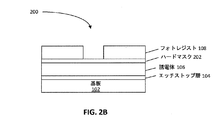
図2Aは、同じくダイまたは他のデバイスとすることができ、基板102と、エッチストップ層104と、誘電体層106と、ハードマスク層202と、フォトレジスト層108とを含むウェハ200を示す。図1A〜図1Eと同様に、フォトレジスト層108は図2Bに示されるようにパターニングされる。
FIG. 2A shows a
図2Cは、フォトレジスト層108のパターンのハードマスク層202への転写を示す。デュアルダマシンプロセスのこの部分は、いくつかの設計において、ハードマスクエッチングまたはトレンチエッチングとして知られている場合がある。
FIG. 2C shows the transfer of the pattern of the
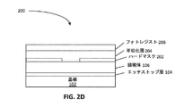
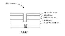
図2Dは、ウェハ200に被着される平坦化層204および第2のフォトレジスト層206を示す。デュアルダマシンプロセスにおいて、平坦化層204はハードマスク層202のエッチングされた部分を保護するために、トレンチエッチング内に配置される。図2Eは、第2のパターンが第2のフォトレジスト層206に転写されることを示しており、それはビアをパターニングすると言われる場合もある。図2Fは、平坦化層204と、ハードマスク層202と、誘電体層106の少なくとも一部とを貫通する、第2のパターン、すなわち、ビアパターンの部分的エッチングを示す。
FIG. 2D shows a planarization layer 204 and a second photoresist layer 206 that are deposited on the
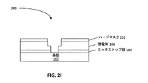
図2Gは、ウェハ200からの第2のフォトレジスト層206および平坦化層204の除去を示す。図2Hは、誘電体層106内のインターコネクトのトレンチ部分を画定する、誘電体層106の別のエッチングを示す。また、誘電体層106内のエッチのビア部分は、誘電体層106を貫通してエッチストップ層104まで延長される。
FIG. 2G shows the removal of the second photoresist layer 206 and the planarization layer 204 from the
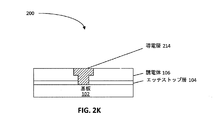
図2Iは、エッチストップ層104の露出した部分をエッチングすることによってインターコネクトのビア部分の底部を開口することを示す。このエッチングは、ここで、基板102を露出させる。図2Jは、エッチストップ層104、誘電体層106およびハードマスク層202内のエッチングされた体積空間内への導電層214の堆積を示す。導電層214は、図1A〜図1Eにおいて説明された導電層122と同様に処理することができる。図2Kは、導電層214およびハードマスク層202の一部の除去を示す。この除去は、化学機械平坦化(CMP)、エッチングまたは他のプロセスを通して実行することができる。
FIG. 2I illustrates opening the bottom of the interconnect via portion by etching the exposed portion of the
図2A〜図2Kにおいて、デュアルダマシンプロセスに対する「trench first with hard mask」(TFHM)手法が説明される。TFHMプロセスが説明されるが、本開示の範囲から逸脱することなく、「trench first then via」または「via first then trench」プロセスまたは他のデュアルダマシンプロセスのような他のデュアルダマシンプロセスが使用される場合もある。 2A-2K, a “trench first with hard mask” (TFHM) approach for a dual damascene process is described. Although a TFHM process is described, other dual damascene processes may be used, such as a “trench first than via” or “via first then trench” process or other dual damascene processes without departing from the scope of this disclosure In some cases.
図1A〜図1Eおよび図2A〜図2Kに示されるプロセスは、導電層が基板102に達することを示すが、ダマシンプロセスを用いて作製される導電層は、ミドルオブライン内で、またはバックエンドオブラインからミドルオブラインインターコネクト層の中で使用される場合もある。
The processes shown in FIGS. 1A-1E and 2A-2K show that the conductive layer reaches the
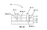
図3は、本開示の一態様によるインターコネクト層を示す。デバイス300は誘電体層106を含み、その中に、第1のMOLインターコネクト層302および第2のMOLインターコネクト層304が設けられる。第1のMOLインターコネクト層302に到達するために、シングルダマシンプロセス(図1A〜図1Fにおいて示されるプロセスに類似)が使用される場合がある。第1のビア320が開口され、第1の導電性材料306で充填される。第1の導電性材料306は、大きなアスペクト比を有するビア320(たとえば、ビアの深さがビアの幅の2倍より大きい)の中に堆積するか、または別の方法で配置することができる材料とすることができる。
FIG. 3 illustrates an interconnect layer according to one aspect of the present disclosure.
第2のMOLインターコネクト層304に到達するために、デュアルダマシンプロセス(図2A〜図2Kに示されるプロセスに類似)が使用される場合がある。さらに、このプロセスは、第1のビア320の第1の導電性材料306に到達するために使用される場合もある。誘電体層308がパターニングされ、開口部が第2の導電性材料310で満たされ、第2のビア330および第1の導電性インターコネクト層340(340−1、340−2)が形成される。第1の導電性インターコネクト層340−1は、第2のビア330を通して、第2のMOLインターコネクト層304に到達する。この構成において、第2の導電性材料310の第1の導電性インターコネクト層340−2は、第1の導電性材料306の第1のビア320を通して第1のMOLインターコネクト層302に到達する。誘電体層308内の開口部は誘電体層106のアスペクト比とは異なるアスペクト比を有する場合があるので、第2の導電性材料310は第1の導電性材料306とは異なる材料である場合がある。さらに、第2の導電性材料310は、導電率、またはデバイス300内の他の層との所望の相互作用/所望の非相互作用のような材料特性に基づいて選択される場合がある。
To reach the second
図3に示されるように、第1のMOLインターコネクト層302に到達するために使用されるデュアルダマシンプロセスは、第2のMOLインターコネクト層304に到達するために使用されるシングルダマシンプロセスの一部としての役割も果たす。その場合に、異なる変数に基づいて、異なる材料が異なるインターコネクト層に到達する場合がある。ビアのアスペクト比によって、特定の材料の使用(たとえば、タングステン)が指定される場合がある。第1のビア320および第2のビア330の第1の導電性材料306および第2の導電性材料310を通してアクセスされる回路のタイミングは、極めて重大な場合がある。結果として、第1のビア320および第2のビア330のサイズ、および特定の第1のMOLインターコネクト層302に到達する第1の導電性材料および第2の導電性材料の材料特性を、本開示のこの態様を通して選択することができる。
As shown in FIG. 3, the dual damascene process used to reach the first
したがって、本開示の一態様は、ハイブリッドビア構造、およびハイブリッドビア構造を形成するプロセスを説明する。デバイス300上のいくつかのインターコネクト層302の場合に、シングルダマシンプロセスを用いて第1のMOLインターコネクト層302への第1のビア320を形成するために、第1の導電性材料306が堆積される。第2のMOLインターコネクト層304の場合に、第2のMOLインターコネクト層304への第2のビア330を形成するために、デュアルダマシンプロセスを用いて、第2の導電性材料310を堆積する。また、第2の導電性材料310は、第1の導電性材料306に結合することもできる。本開示のこの態様は、相互接続のうちのいくつかの相互接続の抵抗を下げることができ、回路の全体性能を高めることができる。第1の導電性インターコネクト層340は、デバイス300内の第1の導電層(たとえば、金属1(M1))とすることもできる。
Accordingly, one aspect of the present disclosure describes a hybrid via structure and a process for forming a hybrid via structure. In the case of
図4は、本開示の一態様による、ミドルオブライン(MOL)層を製造するための方法400を示すプロセスフロー図である。ブロック402において、第1のレベルにある第1のMOLインターコネクト層に結合される、第1の材料の第1のビアがシングルダマシンプロセスにおいて製造される。たとえば、図3に示されるように、第1のビア320が開口され、第1の導電性材料306で満たされる。
FIG. 4 is a process flow diagram illustrating a
ブロック404において、第2の材料の第2のビアおよび第1の導電層がデュアルダマシンプロセスで製造される。たとえば、図3に示されるように、第2のMOLインターコネクト層304への第2のビア330を形成するために、誘電体層308がパターニングされ、開口部が第2の導電性材料310で満たされる。第1の導電性インターコネクト層340−2の第2の導電性材料310は、第1の導電性材料306の第1のビア320を通して、第1のMOLインターコネクト層302にも到達する。第1の導電性材料306は第2の導電性材料310とは異なる場合がある。たとえば、誘電体層308内の開口部は誘電体層106のアスペクト比とは異なるアスペクト比を有する場合があるので、第2の導電性材料310は第1の導電性材料306とは異なる材料である場合がある。この例では、第2の導電性材料310の第2のビア330は、第1の導電性インターコネクト層340−1を第2のMOLインターコネクト層304に結合する。
At
本開示のさらなる態様によれば、半導体インターコネクトが説明される。インターコネクトは、シングルダマシンプロセスにおいて第1の導電性材料で製造された、第1の導電性インターコネクト層と第1のレベルにある第1のミドルオブライン(MOL)インターコネクト層との間の電流を伝導させるための手段を含む。第1の手段は、図3に示されるビア320とすることができる。また、そのデバイスは、デュアルダマシンプロセスにおいて第2の導電性材料で製造された、第1の導電性インターコネクト層と第2のレベルにある少なくとも第2のMOLインターコネクト層との間の電流を伝導させるための手段も含み、第1の導電性材料は第2の導電性材料とは異なる。第2の手段は、図3に示されるビア330とすることができる。別の態様では、前述の手段は、前述の手段によって列挙された機能を実行するように構成される任意のモジュールまたは任意の装置とすることができる。 According to a further aspect of the present disclosure, a semiconductor interconnect is described. The interconnect conducts current between a first conductive interconnect layer and a first middle-of-line (MOL) interconnect layer at a first level, made of a first conductive material in a single damascene process. Means for making it happen. The first means may be the via 320 shown in FIG. The device also conducts current between a first conductive interconnect layer and at least a second MOL interconnect layer at a second level made of a second conductive material in a dual damascene process. The first conductive material is different from the second conductive material. The second means may be the via 330 shown in FIG. In another aspect, the aforementioned means may be any module or any device configured to perform the functions listed by the aforementioned means.
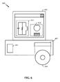
図5は、本開示の一態様を有利に利用することができる例示的なワイヤレス通信システム500を示すブロック図である。例示として、図5は、3つの遠隔ユニット520、530および550と、2つの基地局540とを示している。ワイヤレス通信システムが、より多くの遠隔ユニットおよび基地局を有することができることは認識されよう。遠隔ユニット520、530および550は、開示されるデバイスを含むICデバイス525A、525C、および525Bを含む。基地局、スイッチングデバイス、ネットワーク機器などの他のデバイスも、開示されたデバイスを含むことができることは認識されよう。図5は、基地局540から遠隔ユニット520、530、および550への順方向リンク信号580、ならびに遠隔ユニット520、530、および550から基地局540への逆方向リンク信号590を示す。
FIG. 5 is a block diagram illustrating an example
図5では、ワイヤレスローカルループシステムにおいて、遠隔ユニット520は携帯電話として示され、遠隔ユニット530はポータブルコンピュータとして示され、遠隔ユニット550は定置遠隔ユニットとして示されている。たとえば、遠隔ユニットは、携帯電話、ハンドヘルドパーソナル通信システム(PCS)ユニット、携帯情報端末などのポータブルデータユニット、GPS対応デバイス、ナビゲーションデバイス、セットトップボックス、音楽プレーヤ、ビデオプレーヤ、エンターテインメントユニット、検針機器などの定置データユニット、またはデータもしくはコンピュータ命令を記憶する、もしくは取り出す他のデバイス、またはそれらの組合せとすることができる。図5は本開示の態様による遠隔ユニットを示すが、本開示は、これらの示された例示的なユニットには限定されない。本開示の態様は、開示されたデバイスを含む、多くのデバイスにおいて適切に利用することができる。
In FIG. 5, in a wireless local loop system,
図6は、上で開示されたデバイスのような、半導体構成要素の回路設計、レイアウト設計、および論理設計のために使用される、設計用ワークステーションを示すブロック図である。設計用ワークステーション600は、オペレーティングシステムソフトウェア、サポートファイル、およびCadenceまたはOrCADのような設計ソフトウェアを収容する、ハードディスク601を含む。設計用ワークステーション600はまた、本開示の一態様によるデバイスなどの、回路610または半導体構成要素612の設計を容易にするために、ディスプレイ602を含む。記憶媒体604が、回路610または半導体構成要素612の設計を有形に記憶するために設けられる。回路610または半導体構成要素612の設計は、GDSIIまたはGERBERなどのファイルフォーマットで記憶媒体604上に記憶することができる。記憶媒体604は、CD−ROM、DVD、ハードディスク、フラッシュメモリ、または他の適切なデバイスとすることができる。さらに、設計用ワークステーション600は、記憶媒体604からの入力を受け取るか、または記憶媒体604に出力を書き込むためのドライブ装置603を含む。
FIG. 6 is a block diagram illustrating a design workstation used for circuit design, layout design, and logic design of semiconductor components, such as the devices disclosed above. The
記憶媒体604上に記録されるデータは、論理回路構成、フォトリソグラフィマスク用のパターンデータ、または電子ビームリソグラフィなどの連続描画ツール用のマスクパターンデータを指定することができる。データはさらに、論理シミュレーションに関連付けられるタイミング図やネット回路などの論理検証データも含むことができる。記憶媒体604上のデータを与えることは、半導体ウェハを設計するためのプロセス数を減らすことによって、回路610または半導体構成要素612の設計を容易にする。
Data recorded on the
ファームウェアおよび/またはソフトウェアの実装形態の場合、方法は、本明細書において説明された機能を実行するモジュール(たとえば、手続き、機能など)で実現することができる。本明細書において説明される方法を実施する際に、命令を有形に具現する機械可読媒体を使用することができる。たとえば、ソフトウェアコードは、メモリに記憶することができ、プロセッサユニットによって実行することができる。メモリは、プロセッサユニット内に、またはプロセッサユニットの外部に実装することができる。本明細書において使用されるときに、「メモリ」という用語は、長期メモリ、短期メモリ、揮発性メモリ、不揮発性メモリ、または他のメモリのタイプを指し、特定のタイプのメモリもしくは特定の数のメモリ、またはメモリが格納される媒体のタイプに限定されるべきではない。 For a firmware and / or software implementation, the method may be implemented with modules (eg, procedures, functions, etc.) that perform the functions described herein. In performing the methods described herein, a machine-readable medium that tangibly embodies instructions may be used. For example, software code can be stored in a memory and executed by a processor unit. The memory can be implemented within the processor unit or external to the processor unit. As used herein, the term “memory” refers to a type of long-term memory, short-term memory, volatile memory, non-volatile memory, or other memory, and a specific type of memory or a specific number of It should not be limited to memory or the type of medium on which the memory is stored.
機能が、ファームウェアおよび/またはソフトウェアにおいて実施される場合には、コンピュータ可読媒体上に1つまたは複数の命令またはコードとして記憶することができる。例として、データ構造体で符号化されたコンピュータ可読媒体、およびコンピュータプログラムで符号化されたコンピュータ可読媒体がある。コンピュータ可読媒体は、物理的なコンピュータ記憶媒体を含む。記憶媒体は、コンピュータによってアクセスできる入手可能な媒体とすることができる。限定ではなく、例として、そのようなコンピュータ可読媒体は、RAM、ROM、EEPROM、CD−ROM、または他の光ディスク記憶装置、磁気ディスク記憶装置もしくは他の磁気記憶デバイス、または命令またはデータ構造の形態で所望のプログラムコードを記憶するために使用することができ、コンピュータによってアクセスすることができる他の媒体を含むことができ、本明細書で使用するディスク(disk)およびディスク(disc)は、コンパクトディスク(disc)(CD)、レーザーディスク(登録商標)(disc)、光ディスク(disc)、デジタル多用途ディスク(disc)(DVD)、フロッピーディスク(disk)、およびブルーレイディスク(disc)を含み、ディスク(disk)は、通常、データを磁気的に再生し、一方、ディスク(disc)は、データをレーザで光学的に再生する。上記のものの組合せも、コンピュータ可読媒体の範囲内に含まれるべきである。 If the functionality is implemented in firmware and / or software, it can be stored as one or more instructions or code on a computer-readable medium. Examples include computer readable media encoded with a data structure and computer readable media encoded with a computer program. Computer-readable media includes physical computer storage media. A storage media may be any available media that can be accessed by a computer. By way of example, and not limitation, such computer-readable media can be RAM, ROM, EEPROM, CD-ROM, or other optical disk storage, magnetic disk storage or other magnetic storage device, or in the form of instructions or data structures. Can include other media that can be used to store desired program code and can be accessed by a computer, and the disks and disks used herein are compact Discs, including discs (CD), laser discs (discs), optical discs (discs), digital versatile discs (DVDs), floppy discs (discs), and Blu-ray discs (discs) (Disk) Reproduce data magnetically, while discs (while discs) is reproduce data optically with lasers. Combinations of the above should also be included within the scope of computer-readable media.
命令および/またはデータは、コンピュータ可読媒体上の記憶域に加えて、通信装置に含まれる伝送媒体上の信号として与えることもできる。たとえば、通信装置は、命令およびデータを示す信号を有する送受信機を含むことができる。命令およびデータは、1つまたは複数のプロセッサに、特許請求の範囲において概説される機能を実施させるように構成される。 The instructions and / or data may be provided as signals on a transmission medium included in the communication device, in addition to storage on the computer-readable medium. For example, the communication device can include a transceiver having signals indicative of instructions and data. The instructions and data are configured to cause one or more processors to perform the functions outlined in the claims.
本開示およびその利点について詳細に説明してきたが、添付の特許請求の範囲によって定められるような本開示の技術から逸脱することなく、本明細書において種々の変更、置換、および改変を行うことができることは理解されたい。たとえば、「上」および「下」などの関係性の用語が、基板または電子デバイスに関して使用される。当然、基板または電子デバイスが反転した場合、上は下に、下は上になる。加えて、横向きの場合、上および下は、基板または電子デバイスの側面を指す場合がある。その上、本出願の範囲は、本明細書において説明されたプロセス、機械、製造、組成物、手段、方法およびステップの特定の構成に限定されることを意図していない。当業者が本開示から容易に理解するように、本明細書において説明される対応する構成と実質的に同じ機能を果たすか、もしくは実質的に同じ結果を達成する、現存するもしくは今後開発されるプロセス、機械、製造、組成物、手段、方法、またはステップを、本開示に従って利用することができる。したがって、添付の特許請求の範囲は、そのようなプロセス、機械、製造、組成物、手段、方法、またはステップをその範囲内に含むことを意図している。 Although the present disclosure and its advantages have been described in detail, various changes, substitutions, and alterations may be made herein without departing from the technology of the present disclosure as defined by the appended claims. Please understand that you can. For example, relationship terms such as “above” and “below” are used with respect to a substrate or electronic device. Of course, if the substrate or electronic device is flipped, the top is down and the bottom is up. In addition, when in landscape orientation, top and bottom may refer to the sides of the substrate or electronic device. Moreover, the scope of the present application is not intended to be limited to the particular configuration of processes, machines, manufacture, compositions, means, methods, and steps described herein. As will be readily appreciated by those skilled in the art from this disclosure, an existing or future development that performs substantially the same function or achieves substantially the same results as the corresponding configuration described herein. Any process, machine, manufacture, composition, means, method, or step may be utilized in accordance with the present disclosure. Accordingly, the appended claims are intended to include within their scope such processes, machines, manufacture, compositions of matter, means, methods, or steps.
本明細書の開示に関連して説明された種々の例示的論理ブロック、モジュール、回路、およびアルゴリズムステップが、電子ハードウェア、コンピュータソフトウェア、または両方の組合せとして実現される場合があることは、当業者であればさらに理解されよう。ハードウェアとソフトウェアのこの互換性を明確に示すために、種々の例示的な構成要素、ブロック、モジュール、回路、およびステップが、全般にそれらの機能に関してこれまで説明されてきた。そのような機能がハードウェアとして実現されるか、ソフトウェアとして実現されるかは、特定の用途およびシステム全体に課せられる設計制約によって決まる。当業者は、説明した機能を特定の適用例ごとに様々な方法で実現できるが、そのような実装形態の決定は、本開示の範囲からの逸脱を引き起こすものと解釈されるべきではない。 It should be noted that the various exemplary logic blocks, modules, circuits, and algorithm steps described in connection with the disclosure herein may be implemented as electronic hardware, computer software, or a combination of both. It will be further understood by the contractor. To clearly illustrate this interchangeability of hardware and software, various illustrative components, blocks, modules, circuits, and steps have been described above generally in terms of their functionality. Whether such functionality is implemented as hardware or software depends on the particular application and design constraints imposed on the overall system. Those skilled in the art can implement the described functionality in a variety of ways for each particular application, but such implementation decisions should not be construed as causing deviations from the scope of the present disclosure.
本明細書の開示に関連して説明された種々の例示的な論理ブロック、モジュール、および回路は、本明細書において説明された機能を実行するように設計された汎用プロセッサ、デジタルシグナルプロセッサ(DSP)、特定用途向け集積回路(ASIC)、フィールドプログラマブルゲートアレイ(FPGA)もしくは他のプログラマブル論理デバイス、個別のゲートもしくはトランジスタロジック、個別のハードウェア構成要素、またはそれらの任意の組合せを用いて、実現または実行することができる。汎用プロセッサはマイクロプロセッサとすることができるが、代替形態では、プロセッサは、任意の従来型プロセッサ、コントローラ、マイクロコントローラ、またはステートマシンとすることもできる。プロセッサはまた、コンピューティングデバイスの組合せとして、たとえば、DPSとマイクロプロセッサとの組合せ、複数のマイクロプロセッサ、DSPコアと組み合わせた1つもしくは複数のマイクロプロセッサ、または任意の他のそのような構成として実現することができる。 Various exemplary logic blocks, modules, and circuits described in connection with the disclosure herein are general purpose processors, digital signal processors (DSPs) that are designed to perform the functions described herein. ), Application specific integrated circuit (ASIC), field programmable gate array (FPGA) or other programmable logic device, individual gate or transistor logic, individual hardware components, or any combination thereof Or can be performed. A general purpose processor may be a microprocessor, but in the alternative, the processor may be any conventional processor, controller, microcontroller, or state machine. The processor may also be implemented as a combination of computing devices, eg, a combination of DPS and microprocessor, multiple microprocessors, one or more microprocessors combined with a DSP core, or any other such configuration. can do.
本開示に関連して説明された方法またはアルゴリズムのステップは、ハードウェアにおいて直接、プロセッサによって実行されるソフトウェアモジュールで、またはその2つの組合せにおいて実施することができる。ソフトウェアモジュールは、RAM、フラッシュメモリ、ROM、EPROM、EEPROM、レジスタ、ハードディスク、リムーバブルディスク、CD−ROM、または当技術分野で知られている任意の他の形態の記憶媒体に存在することができる。例示的な記憶媒体は、プロセッサが記憶媒体から情報を読み取り、記憶媒体に情報を書き込むことができるように、プロセッサに結合される。代替形態では、記憶媒体は、プロセッサに一体化することができる。プロセッサおよび記憶媒体は、ASIC内に存在することができる。ASICは、ユーザ端末内に存在することができる。代替形態では、プロセッサおよび記憶媒体は、ユーザ端末内の個別構成要素として存在することができる。 The method or algorithm steps described in connection with the present disclosure may be implemented directly in hardware, in software modules executed by a processor, or in a combination of the two. A software module may reside in RAM, flash memory, ROM, EPROM, EEPROM, registers, hard disk, removable disk, CD-ROM, or any other form of storage medium known in the art. An exemplary storage medium is coupled to the processor such that the processor can read information from, and write information to, the storage medium. In the alternative, the storage medium may be integral to the processor. The processor and the storage medium can reside in an ASIC. The ASIC can exist in the user terminal. In the alternative, the processor and the storage medium may reside as discrete components in a user terminal.
1つまたは複数の例示的な設計では、説明される機能は、ハードウェア、ソフトウェア、ファームウェア、またはそれらの任意の組合せで実現される場合がある。ソフトウェアで実現される場合、機能は、1つまたは複数の命令またはコードとして、コンピュータ可読媒体上に記憶されるか、またはコンピュータ可読媒体を介して送信される場合がある。コンピュータ可読媒体は、コンピュータ記憶媒体と、コンピュータプログラムの1つの場所から別の場所への転送を容易にする任意の媒体を含む通信媒体との両方を含む。記憶媒体は、汎用コンピュータまたは専用コンピュータによってアクセスできる任意の入手可能な媒体とすることができる。限定ではなく例として、そのようなコンピュータ可読媒体は、RAM、ROM、EEPROM、CD−ROMもしくは他の光ディスク記憶装置、磁気ディスク記憶装置もしくは他の磁気記憶デバイス、または命令もしくはデータ構造の形態で規定されたプログラムコード手段を搬送または格納するために使用され得るとともに、汎用もしくは専用コンピュータ、または汎用もしくは専用プロセッサによってアクセスできる任意の他の媒体を含むことができる。また、任意の接続も厳密にはコンピュータ可読媒体と呼ばれる。たとえば、ソフトウェアが、同軸ケーブル、光ファイバーケーブル、ツイストペア、デジタル加入者線(DSL)、または赤外線、無線、およびマイクロ波などのワイヤレス技術を使用してウェブサイト、サーバ、または他のリモートソースから送信される場合、同軸ケーブル、光ファイバーケーブル、ツイストペア、DSL、または赤外線、無線、およびマイクロ波などのワイヤレス技術は、媒体の定義に含まれる。ディスク(disk)およびディスク(disc)は、本明細書において使用されるときに、コンパクトディスク(disc)(CD)、レーザーディスク(登録商標)(disc)、光ディスク(disc)、デジタル多用途ディスク(disc)(DVD)、フロッピーディスク(disk)およびブルーレイディスク(disc)を含み、ディスク(disk)は通常、データを磁気的に再生し、一方、ディスク(disc)は、レーザを用いてデータを光学的に再生する。上記のものの組合せも、コンピュータ可読媒体の範囲内に含まれるべきである。 In one or more exemplary designs, the functions described may be implemented in hardware, software, firmware, or any combination thereof. If implemented in software, the functions may be stored on or transmitted over as one or more instructions or code on a computer-readable medium. Computer-readable media includes both computer storage media and communication media including any medium that facilitates transfer of a computer program from one place to another. A storage media may be any available media that can be accessed by a general purpose or special purpose computer. By way of example, and not limitation, such computer-readable media is defined in the form of RAM, ROM, EEPROM, CD-ROM or other optical disk storage, magnetic disk storage or other magnetic storage device, or instructions or data structures. Can be used to carry or store the programmed program code means and can include any other medium that can be accessed by a general purpose or special purpose computer, or a general purpose or special purpose processor. Any connection is also strictly referred to as a computer-readable medium. For example, software is transmitted from a website, server, or other remote source using coaxial cable, fiber optic cable, twisted pair, digital subscriber line (DSL), or wireless technologies such as infrared, wireless, and microwave In this case, coaxial technology, fiber optic cable, twisted pair, DSL, or wireless technologies such as infrared, radio, and microwave are included in the definition of media. Discs and discs, as used herein, are compact discs (discs) (CDs), laser discs (discs), optical discs (discs), digital versatile discs ( disc) (DVD), floppy disk (disk), and Blu-ray disc (disc), where the disk (disk) typically reproduces data magnetically, while the disc (disc) uses a laser to optically data To play. Combinations of the above should also be included within the scope of computer-readable media.
本開示のこれまでの説明は、当業者が本開示を作製または使用できるようにするために提供される。本開示に対する種々の修正は、当業者に容易に明らかになり、本明細書において規定される一般原理は、本開示の趣旨または範囲を逸脱することなく、他の変形形態に適用される場合がある。したがって、本開示は、本明細書において説明される例および設計に限定されるものではなく、本明細書において開示される原理および新規の特徴に合致する最も広い範囲を与えられるべきである。 The previous description of the disclosure is provided to enable any person skilled in the art to make or use the disclosure. Various modifications to the present disclosure will be readily apparent to those skilled in the art, and the generic principles defined herein may be applied to other variations without departing from the spirit or scope of the disclosure. is there. Accordingly, the present disclosure is not intended to be limited to the examples and designs described herein, but is to be accorded the widest scope consistent with the principles and novel features disclosed herein.
100 ウェハ、ダイ
102 基板
104 エッチストップ層
106 誘電体層
108 フォトレジスト層
110 開口部
112 開口部
114 開口部
116 深さ
118 幅
120 幅
122 導電層
124 誘電体層
200 ウェハ
202 ハードマスク層
204 平坦化層
206 第2のフォトレジスト層
214 導電層
300 デバイス
302 第1のMOLインターコネクト層
304 第2のMOLインターコネクト層
306 第1の導電性材料
308 誘電体層
310 第2の導電性材料
320 第1のビア
330 第2のビア
340 第1の導電性インターコネクト層
340−1 第1の導電性インターコネクト層
340−2 第1の導電性インターコネクト層
500 ワイヤレス通信システム
520 遠隔ユニット
525A ICデバイス
525B ICデバイス
525C ICデバイス
530 遠隔ユニット
540 基地局
550 遠隔ユニット
580 順方向リンク信号
590 逆方向リンク信号
600 設計用ワークステーション
601 ハードディスク
602 ディスプレイ
603 ドライブ装置
604 記憶媒体
610 回路
612 半導体構成要素
100 Wafer,
Claims (30)
シングルダマシンプロセスで製造された、第1の導電性インターコネクト層と第1のレベルにある少なくとも第1のミドルオブライン(MOL)インターコネクト層との間の第1の導電性材料の第1のビアと、
デュアルダマシンプロセスで製造された、前記第1の導電性インターコネクト層と第2のレベルにある少なくとも第2のMOLインターコネクト層との間の第2の導電性材料の第2のビアとを備え、前記第1の導電性材料は前記第2の導電性材料とは異なる、半導体インターコネクト。 A semiconductor interconnect,
A first via of a first conductive material, manufactured in a single damascene process, between the first conductive interconnect layer and at least a first middle of line (MOL) interconnect layer at a first level; ,
A second via of a second conductive material made by a dual damascene process between the first conductive interconnect layer and at least a second MOL interconnect layer at a second level, A semiconductor interconnect, wherein the first conductive material is different from the second conductive material.
シングルダマシンプロセスにおいて、第1のレベルにある第1のMOLインターコネクト層に結合される第1の導電性材料の第1のビアを製造するステップと、
デュアルダマシンプロセスで第2の導電性材料の第2のビアおよび第1の導電性インターコネクト層を製造するステップとを含み、前記第1の導電性インターコネクト層は前記第1のビアに結合し、前記第1の導電性材料は前記第2の導電性材料とは異なり、前記第2のビアは第2のレベルにある第2のMOLインターコネクト層に結合される、方法。 A method of manufacturing a middle of line (MOL) interconnect, comprising:
Producing a first via of a first conductive material coupled to a first MOL interconnect layer at a first level in a single damascene process;
Manufacturing a second via of a second conductive material and a first conductive interconnect layer in a dual damascene process, wherein the first conductive interconnect layer is coupled to the first via, and The method wherein a first conductive material is different from the second conductive material and the second via is coupled to a second MOL interconnect layer at a second level.
シングルダマシンプロセスにおいて、第1のレベルにある第1のMOLインターコネクト層に結合される、第1の導電性材料の第1のビアを製造するためのステップと、
デュアルダマシンプロセスで第2の導電性材料の第2のビアおよび第1の導電性インターコネクト層を製造するためのステップとを含み、前記第1の導電性インターコネクト層は前記第1のビアに結合し、前記第1の導電性材料は前記第2の導電性材料とは異なり、前記第2のビアは第2のレベルにある第2のMOLインターコネクト層に結合される、方法。 A method of manufacturing a middle of line (MOL) interconnect, comprising:
Manufacturing a first via of a first conductive material coupled to a first MOL interconnect layer at a first level in a single damascene process;
Manufacturing a second via of a second conductive material and a first conductive interconnect layer in a dual damascene process, wherein the first conductive interconnect layer is coupled to the first via. , Wherein the first conductive material is different from the second conductive material, and the second via is coupled to a second MOL interconnect layer at a second level.
シングルダマシンプロセスにおいて第1の導電性材料で製造された、第1の導電性インターコネクト層と第1のレベルにある少なくとも第1のミドルオブライン(MOL)インターコネクト層との間の電流を伝導させるための手段と、
デュアルダマシンプロセスにおいて第2の導電性材料で製造された、前記第1の導電性インターコネクト層と第2のレベルにある少なくとも第2のMOLインターコネクト層との間の電流を伝導させるための手段とを備え、前記第1の導電性材料は前記第2の導電性材料とは異なる、半導体インターコネクト。 A semiconductor interconnect,
To conduct current between a first conductive interconnect layer made of a first conductive material in a single damascene process and at least a first middle-of-line (MOL) interconnect layer at a first level. Means of
Means for conducting current between said first conductive interconnect layer and at least a second MOL interconnect layer at a second level made of a second conductive material in a dual damascene process; A semiconductor interconnect, wherein the first conductive material is different from the second conductive material.
Applications Claiming Priority (3)
| Application Number | Priority Date | Filing Date | Title |
|---|---|---|---|
| US14/274,470 US9196583B1 (en) | 2014-05-09 | 2014-05-09 | Via material selection and processing |
| US14/274,470 | 2014-05-09 | ||
| PCT/US2015/024083 WO2015171223A1 (en) | 2014-05-09 | 2015-04-02 | Via material selection and processing |
Publications (2)
| Publication Number | Publication Date |
|---|---|
| JP2017516305A true JP2017516305A (en) | 2017-06-15 |
| JP2017516305A5 JP2017516305A5 (en) | 2018-04-26 |
Family
ID=52875811
Family Applications (1)
| Application Number | Title | Priority Date | Filing Date |
|---|---|---|---|
| JP2016565680A Pending JP2017516305A (en) | 2014-05-09 | 2015-04-02 | Via material selection and processing |
Country Status (5)
| Country | Link |
|---|---|
| US (1) | US9196583B1 (en) |
| EP (1) | EP3140857A1 (en) |
| JP (1) | JP2017516305A (en) |
| CN (1) | CN107004636B (en) |
| WO (1) | WO2015171223A1 (en) |
Families Citing this family (3)
| Publication number | Priority date | Publication date | Assignee | Title |
|---|---|---|---|---|
| US9620454B2 (en) * | 2014-09-12 | 2017-04-11 | Qualcomm Incorporated | Middle-of-line (MOL) manufactured integrated circuits (ICs) employing local interconnects of metal lines using an elongated via, and related methods |
| US9793212B2 (en) * | 2015-04-16 | 2017-10-17 | Taiwan Semiconductor Manufacturing Company, Ltd. | Interconnect structures and methods of forming same |
| WO2019089045A1 (en) * | 2017-11-03 | 2019-05-09 | Intel Corporation | Techniques for forming vias and other interconnects for integrated circuit structures |
Citations (5)
| Publication number | Priority date | Publication date | Assignee | Title |
|---|---|---|---|---|
| JPH06283613A (en) * | 1992-10-20 | 1994-10-07 | Hyundai Electron Ind Co Ltd | Method for forming metallic contact of semiconductor element |
| JP2000100975A (en) * | 1998-09-18 | 2000-04-07 | Nec Corp | Non-volatile semiconductor memory device and manufacture thereof |
| JP2002319625A (en) * | 2001-04-23 | 2002-10-31 | Toshiba Corp | Semiconductor device and manufacturing method therefor |
| WO2004061947A1 (en) * | 2002-12-27 | 2004-07-22 | Fujitsu Limited | Semiconductor device, dram integrated circuit device, and its manufacturing method |
| JP2010087350A (en) * | 2008-10-01 | 2010-04-15 | Fujitsu Microelectronics Ltd | Semiconductor device, and method of manufacturing the same |
Family Cites Families (15)
| Publication number | Priority date | Publication date | Assignee | Title |
|---|---|---|---|---|
| US6974766B1 (en) | 1998-10-01 | 2005-12-13 | Applied Materials, Inc. | In situ deposition of a low κ dielectric layer, barrier layer, etch stop, and anti-reflective coating for damascene application |
| US6261960B1 (en) | 2000-04-06 | 2001-07-17 | Advanced Micro Devices, Inc | High density contacts having rectangular cross-section for dual damascene applications |
| US20050285269A1 (en) | 2004-06-29 | 2005-12-29 | Yang Cao | Substantially void free interconnect formation |
| US7160772B2 (en) | 2005-02-23 | 2007-01-09 | International Business Machines Corporation | Structure and method for integrating MIM capacitor in BEOL wiring levels |
| US7863188B2 (en) * | 2005-07-29 | 2011-01-04 | Semiconductor Energy Laboratory Co., Ltd. | Semiconductor device and manufacturing method thereof |
| US20070218685A1 (en) | 2006-03-17 | 2007-09-20 | Swaminathan Sivakumar | Method of forming trench contacts for MOS transistors |
| US7767570B2 (en) * | 2006-03-22 | 2010-08-03 | Taiwan Semiconductor Manufacturing Company, Ltd. | Dummy vias for damascene process |
| US7602027B2 (en) * | 2006-12-29 | 2009-10-13 | Semiconductor Components Industries, L.L.C. | Semiconductor component and method of manufacture |
| US8089160B2 (en) * | 2007-12-12 | 2012-01-03 | International Business Machines Corporation | IC interconnect for high current |
| JP5554951B2 (en) | 2008-09-11 | 2014-07-23 | ルネサスエレクトロニクス株式会社 | Manufacturing method of semiconductor device |
| US7999320B2 (en) | 2008-12-23 | 2011-08-16 | International Business Machines Corporation | SOI radio frequency switch with enhanced signal fidelity and electrical isolation |
| US7843005B2 (en) | 2009-02-11 | 2010-11-30 | International Business Machines Corporation | SOI radio frequency switch with reduced signal distortion |
| US8133774B2 (en) | 2009-03-26 | 2012-03-13 | International Business Machines Corporation | SOI radio frequency switch with enhanced electrical isolation |
| US8796855B2 (en) * | 2012-01-13 | 2014-08-05 | Freescale Semiconductor, Inc. | Semiconductor devices with nonconductive vias |
| US9355956B2 (en) * | 2013-11-01 | 2016-05-31 | Taiwan Semiconductor Manufacturing Co., Ltd. | Inductor for semiconductor integrated circuit |
-
2014
- 2014-05-09 US US14/274,470 patent/US9196583B1/en active Active
-
2015
- 2015-04-02 WO PCT/US2015/024083 patent/WO2015171223A1/en active Application Filing
- 2015-04-02 CN CN201580020697.1A patent/CN107004636B/en active Active
- 2015-04-02 JP JP2016565680A patent/JP2017516305A/en active Pending
- 2015-04-02 EP EP15716955.8A patent/EP3140857A1/en not_active Withdrawn
Patent Citations (5)
| Publication number | Priority date | Publication date | Assignee | Title |
|---|---|---|---|---|
| JPH06283613A (en) * | 1992-10-20 | 1994-10-07 | Hyundai Electron Ind Co Ltd | Method for forming metallic contact of semiconductor element |
| JP2000100975A (en) * | 1998-09-18 | 2000-04-07 | Nec Corp | Non-volatile semiconductor memory device and manufacture thereof |
| JP2002319625A (en) * | 2001-04-23 | 2002-10-31 | Toshiba Corp | Semiconductor device and manufacturing method therefor |
| WO2004061947A1 (en) * | 2002-12-27 | 2004-07-22 | Fujitsu Limited | Semiconductor device, dram integrated circuit device, and its manufacturing method |
| JP2010087350A (en) * | 2008-10-01 | 2010-04-15 | Fujitsu Microelectronics Ltd | Semiconductor device, and method of manufacturing the same |
Also Published As
| Publication number | Publication date |
|---|---|
| WO2015171223A1 (en) | 2015-11-12 |
| US9196583B1 (en) | 2015-11-24 |
| CN107004636A (en) | 2017-08-01 |
| CN107004636B (en) | 2020-07-28 |
| US20150325515A1 (en) | 2015-11-12 |
| EP3140857A1 (en) | 2017-03-15 |
Similar Documents
| Publication | Publication Date | Title |
|---|---|---|
| JP6317465B2 (en) | Selective formation of conductive barrier layer | |
| JP5859514B2 (en) | Two-sided interconnected CMOS for stacked integrated circuits | |
| JP2017506430A (en) | Dummy gate grounding in a scaled layout design | |
| JP2017512381A (en) | Self-aligned top contact for MRAM manufacturing | |
| JP2017504211A (en) | Stacked conductive interconnect inductor | |
| TWI706442B (en) | Grid self-aligned metal via processing schemes for back end of line (beol) interconnects and structures resulting therefrom | |
| JP2013524534A (en) | Selective patterning for low cost through vias | |
| JP2016512923A (en) | Logic chip with embedded magnetic tunnel junction | |
| KR20130140165A (en) | Fabrication and integration of devices with top and bottom electrodes including magnetic tunnel junctions | |
| JP2018525825A (en) | Metallization process for memory devices | |
| JP2013517629A (en) | Magnetic tunnel junction (MTJ) on planarized electrode | |
| CN104885200A (en) | Techniques for enhancing fracture resistance of interconnects | |
| JP2017516305A (en) | Via material selection and processing | |
| US9691720B2 (en) | Multi-layer ground shield structure of interconnected elements | |
| JP6224844B2 (en) | Conductive layer routing | |
| TW202213687A (en) | Metal interconnect wrap around with graphene | |
| JP2017502496A (en) | High density linear capacitor | |
| WO2021202389A1 (en) | A via zero interconnect layer metal resistor integration | |
| US9478490B2 (en) | Capacitor from second level middle-of-line layer in combination with decoupling capacitors |
Legal Events
| Date | Code | Title | Description |
|---|---|---|---|
| A521 | Request for written amendment filed |
Free format text: JAPANESE INTERMEDIATE CODE: A523 Effective date: 20180315 |
|
| A621 | Written request for application examination |
Free format text: JAPANESE INTERMEDIATE CODE: A621 Effective date: 20180315 |
|
| A131 | Notification of reasons for refusal |
Free format text: JAPANESE INTERMEDIATE CODE: A131 Effective date: 20181221 |
|
| A977 | Report on retrieval |
Free format text: JAPANESE INTERMEDIATE CODE: A971007 Effective date: 20181220 |
|
| A02 | Decision of refusal |
Free format text: JAPANESE INTERMEDIATE CODE: A02 Effective date: 20190708 |