JP2017216325A - Semiconductor device - Google Patents
Semiconductor device Download PDFInfo
- Publication number
- JP2017216325A JP2017216325A JP2016108367A JP2016108367A JP2017216325A JP 2017216325 A JP2017216325 A JP 2017216325A JP 2016108367 A JP2016108367 A JP 2016108367A JP 2016108367 A JP2016108367 A JP 2016108367A JP 2017216325 A JP2017216325 A JP 2017216325A
- Authority
- JP
- Japan
- Prior art keywords
- power supply
- channel mos
- mos transistor
- diode
- wiring
- Prior art date
- Legal status (The legal status is an assumption and is not a legal conclusion. Google has not performed a legal analysis and makes no representation as to the accuracy of the status listed.)
- Pending
Links
Images


Classifications
-
- H—ELECTRICITY
- H02—GENERATION; CONVERSION OR DISTRIBUTION OF ELECTRIC POWER
- H02H—EMERGENCY PROTECTIVE CIRCUIT ARRANGEMENTS
- H02H9/00—Emergency protective circuit arrangements for limiting excess current or voltage without disconnection
- H02H9/04—Emergency protective circuit arrangements for limiting excess current or voltage without disconnection responsive to excess voltage
- H02H9/045—Emergency protective circuit arrangements for limiting excess current or voltage without disconnection responsive to excess voltage adapted to a particular application and not provided for elsewhere
- H02H9/046—Emergency protective circuit arrangements for limiting excess current or voltage without disconnection responsive to excess voltage adapted to a particular application and not provided for elsewhere responsive to excess voltage appearing at terminals of integrated circuits
-
- H—ELECTRICITY
- H01—ELECTRIC ELEMENTS
- H01L—SEMICONDUCTOR DEVICES NOT COVERED BY CLASS H10
- H01L27/00—Devices consisting of a plurality of semiconductor or other solid-state components formed in or on a common substrate
- H01L27/02—Devices consisting of a plurality of semiconductor or other solid-state components formed in or on a common substrate including semiconductor components specially adapted for rectifying, oscillating, amplifying or switching and having at least one potential-jump barrier or surface barrier; including integrated passive circuit elements with at least one potential-jump barrier or surface barrier
- H01L27/0203—Particular design considerations for integrated circuits
- H01L27/0248—Particular design considerations for integrated circuits for electrical or thermal protection, e.g. electrostatic discharge [ESD] protection
- H01L27/0251—Particular design considerations for integrated circuits for electrical or thermal protection, e.g. electrostatic discharge [ESD] protection for MOS devices
- H01L27/0255—Particular design considerations for integrated circuits for electrical or thermal protection, e.g. electrostatic discharge [ESD] protection for MOS devices using diodes as protective elements
-
- H—ELECTRICITY
- H01—ELECTRIC ELEMENTS
- H01L—SEMICONDUCTOR DEVICES NOT COVERED BY CLASS H10
- H01L27/00—Devices consisting of a plurality of semiconductor or other solid-state components formed in or on a common substrate
- H01L27/02—Devices consisting of a plurality of semiconductor or other solid-state components formed in or on a common substrate including semiconductor components specially adapted for rectifying, oscillating, amplifying or switching and having at least one potential-jump barrier or surface barrier; including integrated passive circuit elements with at least one potential-jump barrier or surface barrier
- H01L27/0203—Particular design considerations for integrated circuits
- H01L27/0248—Particular design considerations for integrated circuits for electrical or thermal protection, e.g. electrostatic discharge [ESD] protection
- H01L27/0251—Particular design considerations for integrated circuits for electrical or thermal protection, e.g. electrostatic discharge [ESD] protection for MOS devices
- H01L27/0266—Particular design considerations for integrated circuits for electrical or thermal protection, e.g. electrostatic discharge [ESD] protection for MOS devices using field effect transistors as protective elements
- H01L27/0285—Particular design considerations for integrated circuits for electrical or thermal protection, e.g. electrostatic discharge [ESD] protection for MOS devices using field effect transistors as protective elements bias arrangements for gate electrode of field effect transistors, e.g. RC networks, voltage partitioning circuits
Abstract
Description
本開示は、半導体装置に関し、特に、ESD(Electro Static Discharge:静電気放電)保護に関する。 The present disclosure relates to a semiconductor device, and more particularly to ESD (Electro Static Discharge) protection.
半導体装置において、静電気による内部回路の破壊を防止するために、静電保護素子を設けることが行われている。例えば、電源電位が供給される配線(電源電位線)と接地電位が供給される配線(接地電位線)との間に、ダイオード又はサイリスタ(SCR:Silicon Controlled Rectifier)等によって構成される静電保護素子が接続される。電源電位線と接地電位線との間に静電気が印加されると、静電保護素子を介して静電気が放電されて、内部回路に過大な電圧が印加されることがないので、内部回路の破壊を防止することができる。 In a semiconductor device, an electrostatic protection element is provided in order to prevent destruction of an internal circuit due to static electricity. For example, an electrostatic protection constituted by a diode or a thyristor (SCR: Silicon Controlled Rectifier) between a wiring to which a power supply potential is supplied (power supply potential line) and a wiring to which a ground potential is supplied (ground potential line) Elements are connected. If static electricity is applied between the power supply potential line and the ground potential line, the static electricity is discharged through the electrostatic protection element, so that an excessive voltage is not applied to the internal circuit. Can be prevented.
この点で、特開2003−23084号公報(特許文献1)においては、負電位の入力が可能な構成が示されている。 In this regard, Japanese Patent Laying-Open No. 2003-23084 (Patent Document 1) shows a configuration capable of inputting a negative potential.
一方で、負電位が入力されるような電圧範囲が広範囲な構成の場合には、接地電位線側および電源電位線側にダイオードの段数を増加させる必要が生じ、ダイオードの個数が増加するためレイアウト面積の増加につながるという課題がある。 On the other hand, in the case of a configuration in which the voltage range in which a negative potential is input is wide, it is necessary to increase the number of diode stages on the ground potential line side and the power supply potential line side. There is a problem that it leads to an increase in area.
本開示は、上記の課題を解決するためになされたものであって、簡易な構成でESD耐性を保持することが可能な半導体装置を提供することを目的とする。 The present disclosure has been made to solve the above-described problem, and an object thereof is to provide a semiconductor device capable of maintaining ESD resistance with a simple configuration.
その他の課題と新規な特徴は、本明細書の記述および添付図面から明らかになるであろう。 Other problems and novel features will become apparent from the description of the specification and the accompanying drawings.
一実施例によれば、半導体装置は、電源配線と、接地配線と、電源配線と接地配線との間に接続された入力回路と、入力回路と接続され、接地配線に供給される電圧よりも低い負電圧の入力が可能な入力パッドと、接地配線と、入力パッドとの間に設けられた複数の第1ダイオードと、入力パッドと電源配線との間に設けられた第2ダイオードとを備える。第2ダイオードの逆バイアス降伏電圧は、各第1ダイオードの逆バイアス降伏電圧よりも大きい。 According to one embodiment, the semiconductor device includes a power supply wiring, a ground wiring, an input circuit connected between the power supply wiring and the ground wiring, and a voltage connected to the input circuit and supplied to the ground wiring. An input pad capable of inputting a low negative voltage, a ground wiring, a plurality of first diodes provided between the input pads, and a second diode provided between the input pads and the power supply wiring. . The reverse bias breakdown voltage of the second diode is greater than the reverse bias breakdown voltage of each first diode.
一実施例によれば、簡易な構成でESD耐性を保持することが可能である。 According to one embodiment, it is possible to maintain ESD resistance with a simple configuration.
本実施形態について図面を参照しながら詳細に説明する。なお、図中同一または相当部分には同一符号を付し、その説明は繰り返さない。また、本実施形態において半導体装置とは、電子回路が集積して形成された半導体ウェハ、それを個片化した半導体チップ個々、及び、単一または複数の半導体チップが樹脂等でパッケージされたもの、のいずれをも指す。 The present embodiment will be described in detail with reference to the drawings. In the drawings, the same or corresponding parts are denoted by the same reference numerals, and description thereof will not be repeated. In this embodiment, the semiconductor device is a semiconductor wafer formed by integrating electronic circuits, individual semiconductor chips obtained by dividing the semiconductor wafer, and single or plural semiconductor chips packaged with a resin or the like. Or any of them.
[実施形態1]
図1は、実施形態1に基づく半導体装置1の全体を説明する図である。
[Embodiment 1]
FIG. 1 is a diagram illustrating an
図1に示されるように、半導体装置1は、外周領域に設けられる周回I/O領域4と、内側領域に配置され、所定の機能を有するASIC(application specific integrated circuit)として構成されるコアロジック領域2とを備える。
As shown in FIG. 1, a
周回I/O領域4は、信号の入出力インターフェイスとなるI/Oセル500と、外部電源の入力を受ける電源セル600とが設けられる。ここでは、電源線VMおよび接地線GMが外周領域に配置される場合が示されている。パッドVP,GPが電源用パッド、接地用パッドであり、電源セル600と接続される。パッドSPは、信号用パッドであり、I/Oセル500と接続される。なお、パッドVP,GP,SPは、図1の半導体装置1の周辺に設けられる。
The circular I / O region 4 is provided with an I /
図2は、実施形態1に基づくI/Oセル500および電源セル600の回路構成を説明する図である。
FIG. 2 is a diagram illustrating the circuit configuration of the I /
図2に示されるようにI/Oセル500は、保護ダイオードD1,D2と、PチャネルMOSトランジスタ502と、NチャネルMOSトランジスタ506と、ドライバ504,508と、抵抗510と、入出力回路520とを含む。
As shown in FIG. 2, the I /
パッドSPは、ノードN4と接続される。ノードN4と電源線VMとの間には、保護ダイオードD1が設けられ、アノード側がノードN4と接続され、カソード側が電源線VMと接続される。ここで、パッドSPは、入出力用パッドであり、入力信号を受けることが可能であるとともに、出力信号を出力する。 Pad SP is connected to node N4. A protection diode D1 is provided between the node N4 and the power supply line VM, the anode side is connected to the node N4, and the cathode side is connected to the power supply line VM. Here, the pad SP is an input / output pad, which can receive an input signal and outputs an output signal.
ノードN4と接地線GMとの間には、複数段(3段)の保護ダイオードD2が設けられ、アノード側が接地線GMと接続され、カソード側がノードN4と接続される。抵抗510は、ノードN4と入力回路522との間に設けられる。
A plurality of (three-stage) protection diodes D2 are provided between the node N4 and the ground line GM, the anode side is connected to the ground line GM, and the cathode side is connected to the node N4. The
PチャネルMOSトランジスタ502は、保護ダイオードD1と並列に設けられ、ノードN4と電源線VMとの間に抵抗510を介して直列に接続される。PチャネルMOSトランジスタ502は、ドライバ504の信号の入力を受ける。なお、ドライバ504、508は、インバータを偶数個備えたものであり、電源はそれぞれ電源線VM、接地線GMから供給されている。
P-
NチャネルMOSトランジスタ506は、保護ダイオードD2と並列に設けられ、ノードN4と接地線GMとの間に抵抗510を介して直列に接続される。NチャネルMOSトランジスタ506は、ドライバ508の入力を受ける。
N-
入出力回路520は、電源線VMと接地線GMとの間に設けられる。
入出力回路520は、ドライバ504,508を駆動する出力論理521と、パッドSPからの抵抗510を介する入力信号を処理する入力回路522と、信号レベルを昇圧/降圧するレベルシフタ523とを含む。
The input /
The input /
出力論理521からの信号に従ってドライバ504,508のいずれか一方が動作する。そして、PチャネルMOSトランジスタ502あるいはNチャネルMOSトランジスタ506が導通してパッドSPから信号を出力する。
One of the
電源セル600は、パワークランプ回路(保護回路)を構成するNチャネルMOSトランジスタ604と、インバータ603と、抵抗素子602,609と、容量素子610と、PチャネルMOSトランジスタ606,607,608と、NチャネルMOSトランジスタ611とを含む。ダイオード601は、NチャネルMOSトランジスタ604の寄生ダイオードである。
The
ダイオード601は、アノード側が接地線GMと接続され、カソード側が電源線VMと接続される。
The
NチャネルMOSトランジスタ604は、電源線VMと接地線GMとの間に接続され、そのゲートはインバータ603のノードN2と接続される。
N
PチャネルMOSトランジスタ606は、抵抗素子609およびNチャネルMOSトランジスタ611と、電源線VMと接地線GMとの間に直列に接続される。
P-
PチャネルMOSトランジスタ606は、電源線VMとノードN0との間に設けられ、そのゲートは、ノードN0と接続される。抵抗素子609は、PチャネルMOSトランジスタ606と直列に接続され、一端側はノードN0と接続される。他端側はNチャネルMOSトランジスタ611と接続される。NチャネルMOSトランジスタ611は、抵抗素子609と接地線GMとの間に接続され、そのゲートはノードN2と接続される。
P-
PチャネルMOSトランジスタ607は、PチャネルMOSトランジスタ606とカレントミラー回路を形成するように電源線VMとノードN1との間に設けられ、そのゲートはノードN0と接続される。容量素子610は、ノードN1を介してPチャネルMOSトランジスタ607と直列に電源線VMと接地線GMとの間に接続される。
P-
インバータ603は、ノードN1を入力側としてノードN2にノードN1の反転信号を出力する。なお、インバータ603の電源は図示していないが、電源線VM及び接地線GMから供給されており、他の実施形態でも同様である。
The
抵抗素子602は、ノードN2と接地線GMとの間に接続される。インバータ603の出力は、抵抗素子602を介して接地線GMにプルダウンされているため、インバータ603の出力が不所望に変動した際にNチャネルMOSトランジスタ604のゲート入力が変動することを抑制することが可能である。
NチャネルMOSトランジスタ611は、PチャネルMOSトランジスタ606,607および抵抗素子609で構成されるカレントミラー回路を活性化する素子として機能する。NチャネルMOSトランジスタ611がオンすることによりカレントミラー回路が活性化する。一方、NチャネルMOSトランジスタ611がオフしている場合にはカレントミラー回路は非活性化されている。ここで、カレントミラー回路の活性化とは、カレントミラー回路を構成するトランジスタに電流を流し動作させることであり、他の実施形態でも同様である。ここで、カレントミラー回路の活性化とは、カレントミラー回路を構成するトランジスタに電流を流し動作させることであり、他の実施形態でも同様である。
N-
PチャネルMOSトランジスタ608は、PチャネルMOSトランジスタ607と並列に電源線VMとノードN1との間に接続され、そのゲートはノードN2と接続される。当該PチャネルMOSトランジスタ608は、NチャネルMOSトランジスタ611と相補的に動作する。すなわち、NチャネルMOSトランジスタ611がオンしている場合には、PチャネルMOSトランジスタ608はオフする。一方、NチャネルMOSトランジスタ611がオフしている定常状態の場合には、PチャネルMOSトランジスタ608はオンし、電源線VMとノードN1とを接続して、ノードN1が不所望に変動することを抑制することが可能である。
P-
なお、ここでは、電源セル600の一例として、パワークランプ回路の構成について説明したが特にこれに限られず他の回路を構成しても良い。
Although the configuration of the power clamp circuit has been described as an example of the
ここで、パッドVPにESD電流が流入(印加)される場合について説明する。
定常状態において、インバータ603のノードN2は「L」レベルに設定されている。従って、NチャネルMOSトランジスタ604はオフしている。また、PチャネルMOSトランジスタ608はオンしている。ノードN2は「L」レベルであるためNチャネルMOSトランジスタ611はオフしており、カレントミラー回路は非活性化されている。
Here, a case where an ESD current flows into (applies to) the pad VP will be described.
In the steady state, the node N2 of the
一方、ESD電流による高電圧がパッドVPに印加されると、それに追従して電源線VMのレベルは直接的に変化する。これに伴いインバータ603を構成するPチャネルMOSトランジスタのゲート・ソース間に一時的に電位差(Vgs)を生じ、PチャネルMOSトランジスタがオンする。これにより、ノードN2のレベルは一時的に「L」レベルから「H」レベルに変化する。
On the other hand, when a high voltage due to the ESD current is applied to the pad VP, the level of the power supply line VM changes directly following that. Along with this, a potential difference (Vgs) is temporarily generated between the gate and source of the P-channel MOS
ノードN2のゲート電位の変化に伴って、NチャネルMOSトランジスタ604がオン状態にされ、電源線VMの高電圧が接地線GMに逃がされることになる。
As the gate potential of node N2 changes, N
また、ノードN2のレベルが「H」レベルに変化することに伴い、PチャネルMOSトランジスタ608がオフする。また、NチャネルMOSトランジスタ611がオンとなり、カレントミラー回路が動作する。
Further, as the level of node N2 changes to “H” level, P-
カレントミラー回路の活性化に伴い、PチャネルMOSトランジスタ607を介して電源線VMからノードN1と接続される容量素子610に対して電流が流入する。その際、ノードN1のレベル変化が時定数に従って遅延しながら上昇する。そして、ノードN1の電位がインバータ603の閾値を超えた場合にインバータ603のNチャネルMOSトランジスタがオンする。これにより、ノードN2のレベルは再び「L」レベルに遷移する。
Along with the activation of the current mirror circuit, a current flows from the power supply line VM to the
ノードN2のゲート電位の変化に伴って、NチャネルMOSトランジスタ604がオフ状態にされ、電源線VMから接地線GMへの電流の流出が停止する。また、NチャネルMOSトランジスタ611がオフされ、カレントミラー回路が非活性化される。また、PチャネルMOSトランジスタ608がオンし、ノードN1と電源線VMとが電気的に接続される。これにより、再び定常状態に戻る。
As the gate potential of node N2 changes, N-
ここで、パッドSPに入力される電圧レベルが接地線GMよりも電圧レベルが低い場合について考える。 Here, consider a case where the voltage level input to the pad SP is lower than the ground line GM.
図3は、パッドSPに流れる電流経路を説明する図である。
図3に示されるように、パッドSPに入力される電圧レベルが接地線GMよりも電圧レベルが低い場合には、ダイオードD2を介してESD電流がパッドSPに流れ込むことになる。
FIG. 3 is a diagram for explaining a current path flowing through the pad SP.
As shown in FIG. 3, when the voltage level input to the pad SP is lower than the ground line GM, the ESD current flows into the pad SP via the diode D2.
そのため本構成では、パッドSPに入力される電流を抑制するために複数のダイオードD2を設ける構成としている。 Therefore, in this configuration, a plurality of diodes D2 are provided in order to suppress the current input to the pad SP.
しかしながら、ESD電流が流れる当該構成においては、ノードN4と電源線VMとの間に設けた保護ダイオードD1に対して高い逆バイアス電圧が印加される可能性がある。 However, in the configuration in which the ESD current flows, there is a possibility that a high reverse bias voltage is applied to the protection diode D1 provided between the node N4 and the power supply line VM.
したがって、電源線側にも保護ダイオードD1を複数段設けた場合には回路素子が増加し、回路面積の増大に繋がる。 Therefore, when a plurality of protection diodes D1 are provided also on the power supply line side, the number of circuit elements increases, leading to an increase in circuit area.
それゆえ、実施形態1に従う構成は、保護ダイオードD1と保護ダイオードD2とのダイオード特性を変化させる。 Therefore, the configuration according to the first embodiment changes the diode characteristics of the protection diode D1 and the protection diode D2.
図4は、保護ダイオードD1,D2のダイオード特性を説明する図である。
図4に示されるように、保護ダイオードD1の特性線LAと、保護ダイオードD2の特性線L2とが示されている。
FIG. 4 is a diagram illustrating the diode characteristics of the protection diodes D1 and D2.
As shown in FIG. 4, the characteristic line LA of the protection diode D1 and the characteristic line L2 of the protection diode D2 are shown.
保護ダイオードD1の特性線LAと、保護ダイオードD2の特性線LBとは、逆バイアス降伏電圧(ジャンクション耐圧)の特性が異なる。 The characteristic line LA of the protection diode D1 and the characteristic line LB of the protection diode D2 have different reverse bias breakdown voltage (junction breakdown voltage) characteristics.
具体的には、保護ダイオードD1の特性線LAの方が保護ダイオードD2の特性線LBよりも逆バイアス降伏電圧(ジャンクション耐圧)が高い場合が示されている。 Specifically, the case where the characteristic line LA of the protection diode D1 has a higher reverse bias breakdown voltage (junction breakdown voltage) than the characteristic line LB of the protection diode D2 is shown.
当該特性線LAを有する保護ダイオードD1を設けることにより、個数を増加させることなく保護ダイオードD1を保護することが可能となる。 By providing the protection diode D1 having the characteristic line LA, the protection diode D1 can be protected without increasing the number.
これに伴い、保護ダイオードD1の個数および面積を増加させることなく簡易な構成でESD耐性を保持することが可能な半導体装置を実現することが可能である。 Accordingly, it is possible to realize a semiconductor device capable of maintaining ESD tolerance with a simple configuration without increasing the number and area of the protection diodes D1.
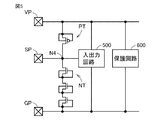
図5は、保護ダイオードD1およびD2を構成する回路構成図である。
図5に示されるように、保護ダイオードD1およびD2をMOSトランジスタとして構成することが可能である。当該構成とすることにより簡易な構成で保護ダイオードD1,D2の面積を縮小することが可能である。
FIG. 5 is a circuit diagram showing the protection diodes D1 and D2.
As shown in FIG. 5, the protection diodes D1 and D2 can be configured as MOS transistors. With this configuration, the areas of the protection diodes D1 and D2 can be reduced with a simple configuration.
具体的には、保護ダイオードD1をソースをゲートと接続したPチャネルMOSトランジスタPTで構成する。保護ダイオードD2をソースをゲートと接続したNチャネルMOSトランジスタNTで構成する。当該構成によりMOSトランジスタのスナップバック動作により高いESD耐性を維持することが可能である。 Specifically, the protection diode D1 is configured by a P-channel MOS transistor PT whose source is connected to the gate. The protection diode D2 is composed of an N channel MOS transistor NT whose source is connected to the gate. With this configuration, it is possible to maintain high ESD resistance by the snapback operation of the MOS transistor.
また、保護ダイオードD1の逆バイアス降伏電圧を高くする方式として、トランジスタのウェル(Well)濃度を調整する。 Further, as a method of increasing the reverse bias breakdown voltage of the protective diode D1, the well concentration of the transistor is adjusted.
具体的には、プロセスチューニングの際に保護ダイオードD1のウェル濃度を保護ダイオードD2のウェル濃度よりも薄く設定するようにしても良い。 Specifically, the well concentration of the protection diode D1 may be set lower than the well concentration of the protection diode D2 during process tuning.
[実施形態2]
上記の実施形態1においては、パッドSPに入力される電圧レベルが接地線GMよりも電圧レベルが低い場合にESD耐性を維持する構成について説明した。
[Embodiment 2]
In the first embodiment described above, the configuration in which the ESD resistance is maintained when the voltage level input to the pad SP is lower than the ground line GM has been described.
一方で、パッドSPに入力される電圧レベルが電源線VMよりも高い場合も考えられる。 On the other hand, there may be a case where the voltage level input to the pad SP is higher than that of the power supply line VM.
図6は、実施形態2に基づく保護ダイオードの構成について説明する図である。
図6を参照して、パッドSPに入力される電圧レベルが電源線VMよりも高い場合には、保護ダイオードD1を保護ダイオードD1#に置換するとともに、ノードN4と接地線GMとの間に保護ダイオードD1#を設ける。また、保護ダイオードD2を保護ダイオードD2#に置換するとともに、ノードN4と電源線VMとの間に複数段(3段)の保護ダイオードD2#を設ける点が異なる。その他の構成については同様であるのでその詳細な説明については繰り返さない。
FIG. 6 is a diagram illustrating a configuration of a protection diode based on the second embodiment.
Referring to FIG. 6, when the voltage level input to pad SP is higher than that of power supply line VM, protection diode D1 is replaced with protection diode D1 # and protection is provided between node N4 and ground line GM. A diode D1 # is provided. Further, the protection diode D2 is replaced with a protection diode D2 #, and a plurality of (three stages) of protection diodes D2 # are provided between the node N4 and the power supply line VM. Since other configurations are the same, detailed description thereof will not be repeated.
本構成の場合には、パッドSPに入力される電圧レベルが電源線VMよりも電圧レベルが高い場合には、ダイオードD2#を介してESD電流が電源線VM側に流れ込むことになる。 In the case of this configuration, when the voltage level input to the pad SP is higher than the power supply line VM, the ESD current flows into the power supply line VM side via the diode D2 #.
そのため本構成では、電源線VM側への電流を抑制するために複数のダイオードD2#を設ける構成としている。 Therefore, in this configuration, a plurality of diodes D2 # are provided in order to suppress a current to the power supply line VM side.
しかしながら、ESD電流が流れる当該構成においては、ノードN4と接地線GMとの間に設けた保護ダイオードD1#に対して高い逆バイアス電圧が印加される可能性がある。 However, in the configuration in which the ESD current flows, a high reverse bias voltage may be applied to the protective diode D1 # provided between the node N4 and the ground line GM.
したがって、接地線側にも保護ダイオードD1#を複数段設けた場合には回路素子が増加し、回路面積の増大に繋がる。 Therefore, when a plurality of protection diodes D1 # are provided on the ground line side, the number of circuit elements increases, leading to an increase in circuit area.
それゆえ、実施形態2に従う構成は、保護ダイオードD1#と保護ダイオードD2#とのダイオード特性を変化させる。 Therefore, the configuration according to the second embodiment changes the diode characteristics of the protection diode D1 # and the protection diode D2 #.
具体的には、実施形態1で説明したように保護ダイオードD1#の逆バイアス降伏電圧(ジャンクション耐圧)を保護ダイオードD2#よりも高く設定する。当該保護ダイオードD1#を設けることにより、個数を増加させることなく保護ダイオードD1#を保護することが可能となる。 Specifically, as described in the first embodiment, the reverse bias breakdown voltage (junction breakdown voltage) of the protection diode D1 # is set higher than that of the protection diode D2 #. By providing the protection diode D1 #, the protection diode D1 # can be protected without increasing the number.
これに伴い、保護ダイオードD1#の個数および面積を増加させることなく簡易な構成でESD耐性を保持することが可能な半導体装置を実現することが可能である。 Accordingly, it is possible to realize a semiconductor device capable of maintaining ESD resistance with a simple configuration without increasing the number and area of the protection diodes D1 #.
以上、本開示を実施形態に基づき具体的に説明したが、本開示は、実施形態に限定されるものではなく、その要旨を逸脱しない範囲で種々変更可能であることはいうまでもない。 As mentioned above, although this indication was concretely demonstrated based on embodiment, it cannot be overemphasized that this indication is not limited to embodiment, and can be variously changed in the range which does not deviate from the summary.
1 半導体装置、2 コアロジック領域、4 周回I/O領域、500 I/Oセル、502,506,604,606,607,608,611,NT トランジスタ、504,508 ドライバ、510 抵抗、520 入出力回路、521 出力論理、522 入力回路、523 レベルシフタ、600 電源セル、601,D1,D2 保護ダイオード、602,609 抵抗素子、603 インバータ、610 容量素子、GM 接地線、GP,SP,VP パッド、VM 電源線。 1 Semiconductor device, 2 core logic area, 4 round I / O area, 500 I / O cell, 502,506,604,606,607,608,611, NT transistor, 504,508 driver, 510 resistance, 520 I / O Circuit, 521 output logic, 522 input circuit, 523 level shifter, 600 power cell, 601, D1, D2 protection diode, 602, 609 resistance element, 603 inverter, 610 capacitance element, GM ground line, GP, SP, VP pad, VM Power line.
Claims (5)
接地配線と、
前記電源配線と前記接地配線との間に接続された入力回路と、
前記入力回路と接続され、前記接地配線に供給される電圧よりも低い負電圧の入力が可能な入力パッドと、
前記接地配線と、前記入力パッドとの間に設けられた複数の第1ダイオードと、
前記入力パッドと前記電源配線との間に設けられた第2ダイオードとを備え、
前記第2ダイオードの逆バイアス降伏電圧は、各前記第1ダイオードの逆バイアス降伏電圧よりも大きい、半導体装置。 Power wiring,
Ground wiring,
An input circuit connected between the power supply wiring and the ground wiring;
An input pad connected to the input circuit and capable of inputting a negative voltage lower than a voltage supplied to the ground wiring;
A plurality of first diodes provided between the ground wiring and the input pad;
A second diode provided between the input pad and the power supply wiring;
The semiconductor device, wherein a reverse bias breakdown voltage of each of the second diodes is greater than a reverse bias breakdown voltage of each of the first diodes.
接地配線と、
前記電源配線と前記接地配線との間に接続された入力回路と、
前記入力回路と接続され、前記電源配線に供給される電圧よりも高い電圧の入力が可能な入力パッドと、
前記電源配線と、前記入力パッドとの間に設けられた複数の第1ダイオードと、
前記入力パッドと前記接地配線との間に設けられた第2ダイオードとを備え、
前記第2ダイオードの逆バイアス降伏電圧は、各前記第1ダイオードの逆バイアス降伏電圧よりも大きい、半導体装置。 Power wiring,
Ground wiring,
An input circuit connected between the power supply wiring and the ground wiring;
An input pad connected to the input circuit and capable of inputting a voltage higher than a voltage supplied to the power supply wiring;
A plurality of first diodes provided between the power supply wiring and the input pad;
A second diode provided between the input pad and the ground wiring;
The semiconductor device, wherein a reverse bias breakdown voltage of each of the second diodes is greater than a reverse bias breakdown voltage of each of the first diodes.
Priority Applications (3)
| Application Number | Priority Date | Filing Date | Title |
|---|---|---|---|
| JP2016108367A JP2017216325A (en) | 2016-05-31 | 2016-05-31 | Semiconductor device |
| US15/480,000 US10361557B2 (en) | 2016-05-31 | 2017-04-05 | Semiconductor device |
| CN201710330480.1A CN107452734A (en) | 2016-05-31 | 2017-05-11 | Semiconductor devices |
Applications Claiming Priority (1)
| Application Number | Priority Date | Filing Date | Title |
|---|---|---|---|
| JP2016108367A JP2017216325A (en) | 2016-05-31 | 2016-05-31 | Semiconductor device |
Publications (2)
| Publication Number | Publication Date |
|---|---|
| JP2017216325A true JP2017216325A (en) | 2017-12-07 |
| JP2017216325A5 JP2017216325A5 (en) | 2019-01-10 |
Family
ID=60420677
Family Applications (1)
| Application Number | Title | Priority Date | Filing Date |
|---|---|---|---|
| JP2016108367A Pending JP2017216325A (en) | 2016-05-31 | 2016-05-31 | Semiconductor device |
Country Status (3)
| Country | Link |
|---|---|
| US (1) | US10361557B2 (en) |
| JP (1) | JP2017216325A (en) |
| CN (1) | CN107452734A (en) |
Families Citing this family (2)
| Publication number | Priority date | Publication date | Assignee | Title |
|---|---|---|---|---|
| CN106449634B (en) * | 2016-09-23 | 2019-06-14 | 矽力杰半导体技术(杭州)有限公司 | Transient Voltage Suppressor and its manufacturing method |
| KR20190140216A (en) * | 2018-06-11 | 2019-12-19 | 에스케이하이닉스 주식회사 | Semiconductor Integrated Circuit Device Including Circuit for Protecting Electro- Static Discharge |
Citations (5)
| Publication number | Priority date | Publication date | Assignee | Title |
|---|---|---|---|---|
| JPH07176735A (en) * | 1993-12-17 | 1995-07-14 | Nec Corp | Input protective circuit of semiconductor circuit |
| JP2001298157A (en) * | 2000-04-14 | 2001-10-26 | Nec Corp | Protection circuit and semiconductor integrated circuit mounting the same |
| JP2010153779A (en) * | 2008-12-24 | 2010-07-08 | Magnachip Semiconductor Ltd | Electrostatic discharge protection circuit |
| JP2013201164A (en) * | 2012-03-23 | 2013-10-03 | Toshiba Corp | Semiconductor device |
| JP2016072349A (en) * | 2014-09-29 | 2016-05-09 | ルネサスエレクトロニクス株式会社 | Semiconductor device |
Family Cites Families (7)
| Publication number | Priority date | Publication date | Assignee | Title |
|---|---|---|---|---|
| US4736271A (en) * | 1987-06-23 | 1988-04-05 | Signetics Corporation | Protection device utilizing one or more subsurface diodes and associated method of manufacture |
| GB2334633B (en) * | 1998-02-21 | 2002-09-25 | Mitel Corp | Low leakage electrostatic discharge protection system |
| JP2003023084A (en) | 2001-07-05 | 2003-01-24 | Matsushita Electric Ind Co Ltd | Esd protection circuit |
| JP4942007B2 (en) * | 2004-10-25 | 2012-05-30 | ルネサスエレクトロニクス株式会社 | Semiconductor integrated circuit |
| JP5232444B2 (en) * | 2007-11-12 | 2013-07-10 | ルネサスエレクトロニクス株式会社 | Semiconductor integrated circuit |
| KR101145785B1 (en) * | 2008-12-26 | 2012-05-16 | 에스케이하이닉스 주식회사 | Integrated circuit |
| US20130003242A1 (en) * | 2010-07-15 | 2013-01-03 | Kun-Hsien Lin | Transient voltage suppressor for multiple pin assignments |
-
2016
- 2016-05-31 JP JP2016108367A patent/JP2017216325A/en active Pending
-
2017
- 2017-04-05 US US15/480,000 patent/US10361557B2/en active Active
- 2017-05-11 CN CN201710330480.1A patent/CN107452734A/en active Pending
Patent Citations (5)
| Publication number | Priority date | Publication date | Assignee | Title |
|---|---|---|---|---|
| JPH07176735A (en) * | 1993-12-17 | 1995-07-14 | Nec Corp | Input protective circuit of semiconductor circuit |
| JP2001298157A (en) * | 2000-04-14 | 2001-10-26 | Nec Corp | Protection circuit and semiconductor integrated circuit mounting the same |
| JP2010153779A (en) * | 2008-12-24 | 2010-07-08 | Magnachip Semiconductor Ltd | Electrostatic discharge protection circuit |
| JP2013201164A (en) * | 2012-03-23 | 2013-10-03 | Toshiba Corp | Semiconductor device |
| JP2016072349A (en) * | 2014-09-29 | 2016-05-09 | ルネサスエレクトロニクス株式会社 | Semiconductor device |
Also Published As
| Publication number | Publication date |
|---|---|
| US10361557B2 (en) | 2019-07-23 |
| CN107452734A (en) | 2017-12-08 |
| US20170346281A1 (en) | 2017-11-30 |
Similar Documents
| Publication | Publication Date | Title |
|---|---|---|
| US7589945B2 (en) | Distributed electrostatic discharge protection circuit with varying clamp size | |
| US7593201B2 (en) | Semiconductor integrated circuit | |
| JP6503395B2 (en) | Electrostatic discharge circuit | |
| JP6308925B2 (en) | Semiconductor device | |
| JP6623139B2 (en) | ESD protection circuit | |
| JP2007234718A (en) | Semiconductor integrated circuit device | |
| KR20120112129A (en) | Esd protection circuit of semiconductor integrated circuit | |
| JP2015002510A (en) | Electrostatic protection circuit | |
| US11411395B2 (en) | Electrostatic discharge protection circuit and operation method | |
| KR102462819B1 (en) | Semiconductor device | |
| US8427798B2 (en) | Semiconductor integrated circuit device | |
| JP2014026996A (en) | Esd protection circuit | |
| CN105575960B (en) | Method and circuit for on-chip electrostatic discharge protection scheme | |
| JP2016167516A (en) | Electrostatic protection circuit | |
| US9812437B2 (en) | Semiconductor integrated circuit device, and electronic appliance using the same | |
| JP2009147040A (en) | Semiconductor integrated circuit device | |
| US10361557B2 (en) | Semiconductor device | |
| JP6784820B2 (en) | ESD protection circuit | |
| JP6461725B2 (en) | Semiconductor device and control method of internal circuit | |
| JP6480051B2 (en) | Semiconductor device | |
| JP6595948B2 (en) | Semiconductor device | |
| KR101131568B1 (en) | Input circuit structure of semiconductor device | |
| JP5819489B2 (en) | Semiconductor device | |
| JP6639631B2 (en) | Semiconductor device and control device | |
| KR100866716B1 (en) | ESD Protection circuit |
Legal Events
| Date | Code | Title | Description |
|---|---|---|---|
| A521 | Request for written amendment filed |
Free format text: JAPANESE INTERMEDIATE CODE: A523 Effective date: 20181120 |
|
| A621 | Written request for application examination |
Free format text: JAPANESE INTERMEDIATE CODE: A621 Effective date: 20181120 |
|
| A977 | Report on retrieval |
Free format text: JAPANESE INTERMEDIATE CODE: A971007 Effective date: 20190913 |
|
| A131 | Notification of reasons for refusal |
Free format text: JAPANESE INTERMEDIATE CODE: A131 Effective date: 20190924 |
|
| A02 | Decision of refusal |
Free format text: JAPANESE INTERMEDIATE CODE: A02 Effective date: 20200317 |