JP2017208530A - Debris-removal groove for cmp polishing pad - Google Patents
Debris-removal groove for cmp polishing pad Download PDFInfo
- Publication number
- JP2017208530A JP2017208530A JP2017056833A JP2017056833A JP2017208530A JP 2017208530 A JP2017208530 A JP 2017208530A JP 2017056833 A JP2017056833 A JP 2017056833A JP 2017056833 A JP2017056833 A JP 2017056833A JP 2017208530 A JP2017208530 A JP 2017208530A
- Authority
- JP
- Japan
- Prior art keywords
- polishing
- grooves
- groove
- supply
- polishing pad
- Prior art date
- Legal status (The legal status is an assumption and is not a legal conclusion. Google has not performed a legal analysis and makes no representation as to the accuracy of the status listed.)
- Granted
Links
Images


Classifications
-
- B—PERFORMING OPERATIONS; TRANSPORTING
- B24—GRINDING; POLISHING
- B24B—MACHINES, DEVICES, OR PROCESSES FOR GRINDING OR POLISHING; DRESSING OR CONDITIONING OF ABRADING SURFACES; FEEDING OF GRINDING, POLISHING, OR LAPPING AGENTS
- B24B37/00—Lapping machines or devices; Accessories
- B24B37/11—Lapping tools
- B24B37/20—Lapping pads for working plane surfaces
- B24B37/26—Lapping pads for working plane surfaces characterised by the shape of the lapping pad surface, e.g. grooved
-
- B—PERFORMING OPERATIONS; TRANSPORTING
- B24—GRINDING; POLISHING
- B24B—MACHINES, DEVICES, OR PROCESSES FOR GRINDING OR POLISHING; DRESSING OR CONDITIONING OF ABRADING SURFACES; FEEDING OF GRINDING, POLISHING, OR LAPPING AGENTS
- B24B37/00—Lapping machines or devices; Accessories
- B24B37/04—Lapping machines or devices; Accessories designed for working plane surfaces
-
- B—PERFORMING OPERATIONS; TRANSPORTING
- B24—GRINDING; POLISHING
- B24B—MACHINES, DEVICES, OR PROCESSES FOR GRINDING OR POLISHING; DRESSING OR CONDITIONING OF ABRADING SURFACES; FEEDING OF GRINDING, POLISHING, OR LAPPING AGENTS
- B24B37/00—Lapping machines or devices; Accessories
- B24B37/11—Lapping tools
- B24B37/12—Lapping plates for working plane surfaces
- B24B37/16—Lapping plates for working plane surfaces characterised by the shape of the lapping plate surface, e.g. grooved
-
- B—PERFORMING OPERATIONS; TRANSPORTING
- B24—GRINDING; POLISHING
- B24B—MACHINES, DEVICES, OR PROCESSES FOR GRINDING OR POLISHING; DRESSING OR CONDITIONING OF ABRADING SURFACES; FEEDING OF GRINDING, POLISHING, OR LAPPING AGENTS
- B24B57/00—Devices for feeding, applying, grading or recovering grinding, polishing or lapping agents
- B24B57/02—Devices for feeding, applying, grading or recovering grinding, polishing or lapping agents for feeding of fluid, sprayed, pulverised, or liquefied grinding, polishing or lapping agents
-
- B—PERFORMING OPERATIONS; TRANSPORTING
- B24—GRINDING; POLISHING
- B24D—TOOLS FOR GRINDING, BUFFING OR SHARPENING
- B24D11/00—Constructional features of flexible abrasive materials; Special features in the manufacture of such materials
-
- H—ELECTRICITY
- H01—ELECTRIC ELEMENTS
- H01L—SEMICONDUCTOR DEVICES NOT COVERED BY CLASS H10
- H01L21/00—Processes or apparatus adapted for the manufacture or treatment of semiconductor or solid state devices or of parts thereof
- H01L21/02—Manufacture or treatment of semiconductor devices or of parts thereof
- H01L21/04—Manufacture or treatment of semiconductor devices or of parts thereof the devices having at least one potential-jump barrier or surface barrier, e.g. PN junction, depletion layer or carrier concentration layer
- H01L21/18—Manufacture or treatment of semiconductor devices or of parts thereof the devices having at least one potential-jump barrier or surface barrier, e.g. PN junction, depletion layer or carrier concentration layer the devices having semiconductor bodies comprising elements of Group IV of the Periodic System or AIIIBV compounds with or without impurities, e.g. doping materials
- H01L21/30—Treatment of semiconductor bodies using processes or apparatus not provided for in groups H01L21/20 - H01L21/26
- H01L21/302—Treatment of semiconductor bodies using processes or apparatus not provided for in groups H01L21/20 - H01L21/26 to change their surface-physical characteristics or shape, e.g. etching, polishing, cutting
- H01L21/304—Mechanical treatment, e.g. grinding, polishing, cutting
-
- H—ELECTRICITY
- H01—ELECTRIC ELEMENTS
- H01L—SEMICONDUCTOR DEVICES NOT COVERED BY CLASS H10
- H01L21/00—Processes or apparatus adapted for the manufacture or treatment of semiconductor or solid state devices or of parts thereof
- H01L21/02—Manufacture or treatment of semiconductor devices or of parts thereof
- H01L21/04—Manufacture or treatment of semiconductor devices or of parts thereof the devices having at least one potential-jump barrier or surface barrier, e.g. PN junction, depletion layer or carrier concentration layer
- H01L21/18—Manufacture or treatment of semiconductor devices or of parts thereof the devices having at least one potential-jump barrier or surface barrier, e.g. PN junction, depletion layer or carrier concentration layer the devices having semiconductor bodies comprising elements of Group IV of the Periodic System or AIIIBV compounds with or without impurities, e.g. doping materials
- H01L21/30—Treatment of semiconductor bodies using processes or apparatus not provided for in groups H01L21/20 - H01L21/26
- H01L21/302—Treatment of semiconductor bodies using processes or apparatus not provided for in groups H01L21/20 - H01L21/26 to change their surface-physical characteristics or shape, e.g. etching, polishing, cutting
- H01L21/306—Chemical or electrical treatment, e.g. electrolytic etching
- H01L21/30625—With simultaneous mechanical treatment, e.g. mechanico-chemical polishing
Abstract
Description
本発明は、ケミカルメカニカル研磨パッドのための溝に関する。より具体的には、本発明は、ケミカルメカニカルポリッシング中の欠陥を減らすための溝設計に関する。 The present invention relates to a groove for a chemical mechanical polishing pad. More specifically, the present invention relates to a groove design to reduce defects during chemical mechanical polishing.
集積回路及び他の電子装置の作製においては、導体、半導体及び絶縁材料の複数の層を半導体ウェーハの表面に付着させたり、半導体ウェーハの表面から除去したりする。導体、半導体及び絶縁材料の薄層は、いくつかの付着技術を使用して付着させることができる。最新のウェーハ加工において一般的な付着技術としては、とりわけ、スパッタリングとも知られる物理蒸着法(PVD)、化学蒸着法(CVD)、プラズマ増強化学蒸着法(PECVD)及び電気化学的めっき法がある。一般的な除去技術としては、とりわけ、湿式及び乾式の等方性及び異方性エッチングがある。 In the fabrication of integrated circuits and other electronic devices, multiple layers of conductors, semiconductors, and insulating materials are deposited on or removed from the surface of the semiconductor wafer. Thin layers of conductors, semiconductors and insulating materials can be deposited using a number of deposition techniques. Common deposition techniques in modern wafer processing include, among others, physical vapor deposition (PVD), also known as sputtering, chemical vapor deposition (CVD), plasma enhanced chemical vapor deposition (PECVD), and electrochemical plating. Common removal techniques include wet and dry isotropic and anisotropic etching, among others.
材料層が順次に付着され、除去されるにつれ、ウェーハの最上面は非平坦になる。後続の半導体加工(たとえばメタライゼーション)は、ウェーハが平坦面を有することを要するため、ウェーハは平坦化されなければならない。平坦化は、望まれない表面トポグラフィーならびに表面欠陥、たとえば粗面、凝集した材料、結晶格子の損傷、スクラッチ及び汚染された層又は材料を除去するのに有用である。 As the material layers are sequentially deposited and removed, the top surface of the wafer becomes non-planar. Since subsequent semiconductor processing (eg, metallization) requires the wafer to have a flat surface, the wafer must be planarized. Planarization is useful for removing unwanted surface topography as well as surface defects such as rough surfaces, agglomerated materials, crystal lattice damage, scratches and contaminated layers or materials.
ケミカルメカニカルプラナリゼーション又はケミカルメカニカルポリッシング(CMP)は、半導体ウェーハのような加工物を平坦化又は研磨するために使用される一般的な技術である。従来のCMPにおいては、ウェーハキャリヤ、すなわち研磨ヘッドがキャリヤアセンブリに取り付けられる。その研磨ヘッドがウェーハを保持し、ウェーハを、CMP装置内でテーブル又はプラテン上に取り付けられている研磨パッドの研磨層と接する状態に配置する。キャリヤアセンブリがウェーハと研磨パッドとの間に制御可能な圧を提供する。同時に、研磨媒(たとえばスラリー)が研磨パッド上に小出しされ、ウェーハと研磨層との間の間隙に引き込まれる。研磨パッド及びウェーハは一般に互いに対して回転して基材を研磨する。研磨パッドがウェーハの下で回転するとき、ウェーハは一般に環状の研磨トラック、すなわち研磨領域を掃き出し、その中でウェーハ表面が研磨層と直接対面する。ウェーハ表面は、研磨層及び表面上の研磨媒の化学的かつ機械的作用によって研磨され、平坦化される。 Chemical mechanical planarization or chemical mechanical polishing (CMP) is a common technique used to planarize or polish workpieces such as semiconductor wafers. In conventional CMP, a wafer carrier, or polishing head, is attached to the carrier assembly. The polishing head holds the wafer and places the wafer in contact with a polishing layer of a polishing pad mounted on a table or platen in a CMP apparatus. A carrier assembly provides a controllable pressure between the wafer and the polishing pad. At the same time, a polishing medium (eg, slurry) is dispensed onto the polishing pad and drawn into the gap between the wafer and the polishing layer. The polishing pad and wafer are typically rotated relative to each other to polish the substrate. As the polishing pad rotates under the wafer, the wafer typically sweeps out an annular polishing track, i.e., a polishing area, in which the wafer surface directly faces the polishing layer. The wafer surface is polished and planarized by the chemical and mechanical action of the polishing layer and the polishing medium on the surface.
Reinhardtらの米国特許第5,578,362号は、パッドにマクロテキスチャを設けるための溝の使用を開示している。特に、多様なパターン、等高線、溝、らせん形、放射状、ドット又は他の形状を開示している。Reinhardtに含まれる具体例は、同心円及びX−Y溝を重ねられた同心円である。同心円状の溝パターンはパッドの縁への直接的な流路を提供しないため、同心円状の溝はもっとも一般的な溝パターンであることがわかった。 Reinhardt et al U.S. Pat. No. 5,578,362 discloses the use of grooves to provide macrotextures in the pad. In particular, various patterns, contours, grooves, spirals, radials, dots or other shapes are disclosed. The specific example contained in Reinhardt is a concentric circle on which concentric circles and XY grooves are overlapped. The concentric groove pattern was found to be the most common groove pattern because the concentric groove pattern does not provide a direct flow path to the pad edge.
Linらは、米国特許第6,120,366号において、円形+半径方向の溝の組み合わせを開示している。この例は、24本の半径方向溝を同心円状の溝パターンに加えることを示す。この溝パターンの欠点は、スラリー使用量の実質的増加のせいで、研磨において限られた改善しか提供しないことである。 Lin et al., In US Pat. No. 6,120,366, discloses a circular + radial groove combination. This example shows the addition of 24 radial grooves to a concentric groove pattern. The disadvantage of this groove pattern is that it offers only a limited improvement in polishing due to a substantial increase in slurry usage.
それにもかかわらず、研磨性能とスラリー使用量とのより良い組み合わせを有するケミカルメカニカル研磨パッドの必要性が絶えずある。さらには、欠陥を減らし、研磨パッド耐用寿命を延ばす溝の必要性がある。 Nevertheless, there is a continuing need for chemical mechanical polishing pads that have a better combination of polishing performance and slurry usage. Furthermore, there is a need for grooves that reduce defects and extend the useful life of the polishing pad.
本発明の態様は、半導体基材、光学基材及び磁性基材の少なくとも一つを、研磨流体及び研磨パッドと半導体基材、光学基材及び磁性基材の少なくとも一つとの間の相対運動によって研磨又は平坦化するのに適した研磨パッドであって、ポリマーマトリックス及び厚さを有する研磨層であって、中心、周縁、中心から周縁まで延びる半径及び中心を包囲し、半径と交差する研磨トラック(半導体基材、光学基材及び磁性基材の少なくとも一つを研磨又は平坦化するための研磨層の作用領域を表す)を含む研磨層と;半径と交差する複数の供給溝(δ)であって、半導体基材、光学基材及び磁性基材の少なくとも一つを研磨パッド及び研磨流体で研磨又は平坦化するためのランドエリアを供給溝(δ)の間に有し、平均供給断面積(δa)(各供給溝の合計断面積を供給溝(δ)の総数で割ったもの)を有する複数の供給溝(δ)と;研磨流体が複数の供給溝(δ)から少なくとも一つの半径方向排流溝(ρ)に流れることを許すための、複数の供給溝(δ)と交差する、研磨層中の少なくとも一つの半径方向排流溝(ρ)とを含み、少なくとも一つの半径方向排流溝(ρ)が平均排流断面積(ρa)を有し、少なくとも一つの半径方向排流溝の平均排流断面積(ρa)が、
2*δa≦ρa≦8*δa
(式中、(nr)は半径方向溝の数を表し、(nf)は供給溝の数を表す)
及び
(0.15)nf*δa≦nr*ρa≦(0.35)nf*δa
にしたがって平均供給断面積(δa)よりも大きく、少なくとも一つの半径方向排流溝(ρ)が研磨トラックを通過して延びて、研磨パッドの回転中、研磨くずを、半導体基材、光学基材及び磁性基材の少なくとも一つの下で、研磨トラックに通し、研磨トラックを越えさせて研磨パッドの周縁へと除去することを促進する、研磨パッドを提供する。
Aspects of the present invention provide that at least one of a semiconductor substrate, an optical substrate and a magnetic substrate is moved by relative movement between the polishing fluid and the polishing pad and at least one of the semiconductor substrate, the optical substrate and the magnetic substrate. A polishing pad suitable for polishing or planarization, a polishing layer having a polymer matrix and a thickness, comprising a center, a periphery, a radius extending from the center to the periphery, and a polishing track surrounding and intersecting the center A polishing layer comprising (representing a working area of the polishing layer for polishing or planarizing at least one of a semiconductor substrate, an optical substrate and a magnetic substrate); a plurality of supply grooves (δ) intersecting the radius A land area for polishing or planarizing at least one of a semiconductor substrate, an optical substrate, and a magnetic substrate with a polishing pad and a polishing fluid between supply grooves (δ), and an average supply cross-sectional area ([delta] a) (each sample A plurality of supply grooves (δ) having a total cross-sectional area of the grooves divided by the total number of supply grooves (δ); and at least one radial drain groove (ρ At least one radial drain groove (ρ) in the polishing layer intersecting the plurality of supply grooves (δ) to allow flow into the at least one radial drain groove (ρ) There has an average drainage cross-sectional area ([rho a), average drainage cross-sectional area of the at least one radial drainage grooves ([rho a) is,
2 * δ a ≦ ρ a ≦ 8 * δ a
( Wherein (n r ) represents the number of radial grooves and (n f ) represents the number of supply grooves)
And (0.15) n f * δ a ≦ n r * ρ a ≦ (0.35) n f * δ a
Is larger than the average supply cross-sectional area (δ a ), and at least one radial drain groove (ρ) extends through the polishing track so that during the rotation of the polishing pad, the polishing debris is removed from the semiconductor substrate, optical A polishing pad is provided that facilitates passing under the at least one of the substrate and the magnetic substrate through the polishing track and over the polishing track to the periphery of the polishing pad.
本発明の代替態様は、半導体基材、光学基材及び磁性基材の少なくとも一つを、研磨流体及び研磨パッドと半導体基材、光学基材及び磁性基材の少なくとも一つとの間の相対運動によって研磨又は平坦化するのに適した研磨パッドであって、ポリマーマトリックス及び厚さを有する研磨層であって、中心、周縁、中心から周縁まで延びる半径及び中心を包囲し、半径と交差する研磨トラック(半導体基材、光学基材及び磁性基材の少なくとも一つを研磨又は平坦化するための研磨層の作用領域を表す)を含む研磨層と;半径と交差する複数の供給溝(δ)であって、半導体基材、光学基材及び磁性基材の少なくとも一つを研磨パッド及び研磨流体で研磨又は平坦化するためのランドエリアを供給溝(δ)の間に有し、平均供給断面積(δa)(各供給溝の合計断面積を供給溝(δ)の総数で割ったもの)を有する複数の供給溝(δ)と;研磨流体が複数の供給溝(δ)から少なくとも一つの半径方向排流溝(ρ)に流れることを許すための、複数の供給溝(δ)と交差する、研磨層中の少なくとも一つの半径方向排流溝(ρ)とを含み、少なくとも一つの半径方向排流溝(ρ)が平均排流断面積(ρa)を有し、少なくとも一つの半径方向排流溝の平均排流断面積(ρa)が、
2*δa≦ρa≦8*δa
(式中、(nr)は半径方向溝の数を表し、(nf)は供給溝の数を表す)
及び
(0.15)nf*δa≦nr*ρa≦(0.35)nf*δa
(式中、nrは数2〜12に等しい)
にしたがって平均供給断面積(δa)よりも大きく、少なくとも一つの半径方向排流溝(ρ)が研磨トラックを通過して延びて、研磨パッドの回転中、研磨くずを、半導体基材、光学基材及び磁性基材の少なくとも一つの下で、研磨トラックに通し、研磨トラックを越えさせて研磨パッドの周縁へと除去することを促進する、研磨パッドを提供する。
An alternative aspect of the present invention is to provide at least one of a semiconductor substrate, an optical substrate and a magnetic substrate, and a relative motion between the polishing fluid and the polishing pad and at least one of the semiconductor substrate, the optical substrate and the magnetic substrate. A polishing pad suitable for polishing or planarizing by means of a polishing layer having a polymer matrix and a thickness, comprising a center, a periphery, a radius extending from the center to the periphery and surrounding the center and intersecting the radius A polishing layer comprising a track (representing a working area of the polishing layer for polishing or planarizing at least one of a semiconductor substrate, an optical substrate and a magnetic substrate); a plurality of supply grooves (δ) intersecting the radius A land area for polishing or planarizing at least one of a semiconductor substrate, an optical substrate and a magnetic substrate with a polishing pad and a polishing fluid between supply grooves (δ), and an average supply interruption area ([delta] a) ( A plurality of supply grooves (δ) having a total cross-sectional area of the supply grooves divided by the total number of supply grooves (δ); and at least one radial drain groove (from which the polishing fluid flows from the plurality of supply grooves (δ)) including at least one radial drain groove (ρ) in the polishing layer that intersects a plurality of supply grooves (δ) to allow flow to ρ), and at least one radial drain groove (ρ ) has an average drainage cross-sectional area ([rho a), average drainage cross-sectional area of the at least one radial drainage grooves ([rho a) is,
2 * δ a ≦ ρ a ≦ 8 * δ a
( Wherein (n r ) represents the number of radial grooves and (n f ) represents the number of supply grooves)
And (0.15) n f * δ a ≦ n r * ρ a ≦ (0.35) n f * δ a
(Where n r is equal to the number 2-12)
Is larger than the average supply cross-sectional area (δ a ), and at least one radial drain groove (ρ) extends through the polishing track so that during the rotation of the polishing pad, the polishing debris is removed from the semiconductor substrate, optical A polishing pad is provided that facilitates passing under the at least one of the substrate and the magnetic substrate through the polishing track and over the polishing track to the periphery of the polishing pad.
詳細な説明
独立気泡パッド材料における除去プロセスは、パッド側に凹凸を含む薄い潤滑膜の中で起こる。除去が起こるためには、凹凸が基材表面と直接的又は半直接的に接触しなければならない。これは、液体輸送及び静水圧の軽減を促進するように表面テキスチャを設計し、排流を促進するように溝又は他の種類のマクロテキスチャを組み込むことによって影響される。うまく制御された接触の維持は、プロセス条件、溝間のランドエリア中のテキスチャの維持及び多様な他の変数に対して相対的に敏感である。
DETAILED DESCRIPTION The removal process in the closed cell pad material occurs in a thin lubricating film that includes irregularities on the pad side. In order for removal to occur, the irregularities must be in direct or semi-direct contact with the substrate surface. This is affected by designing the surface texture to promote liquid transport and hydrostatic pressure relief and incorporating grooves or other types of macrotextures to facilitate drainage. Maintaining well-controlled contact is relatively sensitive to process conditions, texture maintenance in the land area between grooves and a variety of other variables.
現在のパッド中の基材接触ゾーン中の局所環境は以下のような特徴を有する。 The local environment in the substrate contact zone in the current pad has the following characteristics.
表面積/体積比(S/V)はウェーハ側及びパッド側のいずれでも非常に高く、>200:1などである。これが潤滑膜内の液体輸送を非常に困難にする。特に、研磨中の質量除去速度を考慮すると、潤滑膜は、反応体中で有意に消耗し、反応生成物中で有意に富化される。 The surface area / volume ratio (S / V) is very high on both the wafer side and the pad side, such as> 200: 1. This makes liquid transport in the lubricating film very difficult. In particular, considering the mass removal rate during polishing, the lubricating film is significantly consumed in the reactants and is significantly enriched in the reaction products.
液体温度は周囲温度よりもずっと高く、深さ及び横方向勾配が大きい。これは、マクロ及びミクロレベルの有意な詳細において内部的に研究されている。研磨プロセスは多大なエネルギーを消費するが、そのすべてが除去を生じさせるわけではない。液体内の接触又は接触に近い摩擦及び粘性摩擦が有意な接触加熱を発生させる。パッドは効率的な断熱材であるため、発生した熱の大部分は液体中に散逸する。したがって、潤滑膜内の、特に凹凸の近くの局所環境は弱熱水性である。温度勾配が、高いS/Vとともに、特にパッド表面のテキスチャ容積内に反応生成物を沈殿させるための駆動力を提供する。反応生成物はかなり大きくありがちであり、時間とともに成長することが予想されるため、これは、微小スクラッチ欠陥を生じさせる主要な機構の一つとなることができる。モノマー可溶性に対する温度効果が非常に顕著であるため、シリカ沈殿が大きな懸念である。 The liquid temperature is much higher than the ambient temperature, and the depth and lateral gradient are large. This has been studied internally at significant details at the macro and micro levels. Although the polishing process consumes significant energy, not all of it causes removal. Friction in contact with liquid or near friction and viscous friction generate significant contact heating. Since the pad is an efficient thermal insulator, most of the generated heat is dissipated in the liquid. Therefore, the local environment in the lubricating film, particularly near the unevenness, is weakly hot water. The temperature gradient provides a driving force to precipitate the reaction product, especially in the texture volume of the pad surface, with high S / V. This can be one of the main mechanisms that cause micro-scratch defects since the reaction products tend to be quite large and are expected to grow over time. Silica precipitation is a major concern because the temperature effect on monomer solubility is very significant.
基材表面上の点の基準系から、熱及び反応履歴は極端な周期的変動を受ける。この周期的変動に対する有意な寄与が、パッド中の溝の必要性である(ウェーハとの均一な接触に影響するために)。溝中の液体環境はランドエリア中の液体環境とは有意に異なる。有意に冷温であり、反応体が有意に富化され、反応生成物が有意に少ない。したがって、ウェーハ上の各点は、これら二つの非常に異なる環境の間で急速な循環を見る。これは、研磨副生成物を特に接触の後縁でウェーハ表面に再付着させるための駆動力を提供することができる。 From the reference system of points on the substrate surface, the heat and reaction history are subject to extreme periodic variations. A significant contribution to this periodic variation is the need for grooves in the pad (to affect uniform contact with the wafer). The liquid environment in the groove is significantly different from the liquid environment in the land area. Significantly cold, reactants are significantly enriched, and reaction products are significantly less. Thus, each point on the wafer sees a rapid circulation between these two very different environments. This can provide a driving force to reattach the polishing by-product to the wafer surface, particularly at the trailing edge of contact.
ウェーハ接触中、ランドエリアへのスラリー輸送は溝を介して起こる。残念ながら、溝は二つの目的:新鮮なスラリーを供給する目的及び使用済みスラリーを除去する目的を果たす。すべての現在のパッド設計において、これが同じ容積中で同時に起こらなければならない。したがって、ランドは、新鮮なスラリーを供給されず、可変性混合物を供給される。可変性混合物が発生する場所は逆混合ゾーンとして知られる。逆混合ゾーンは、溝設計によって減らすことはできるが、なくすことはできない。これが、スクラッチ及び残渣付着の両方をもたらす大きな粒子のもう一つの有意な発生源となる。最大の懸念は、溝中のスラリーが連続的に更新されず、大きな凝集粒子の形成及び成長が連続的に起こることである。新鮮なスラリーの導入と無計画な液体輸送とが同時にあるならば、これらの大きな粒子は、最終的には、ますます大きな数でランド面に打ち寄せて、スクラッチ欠陥の漸増を生じさせる。この効果は、プロセス条件又はコンディショニングのモードにかかわらず、パッドの使用中に一般に認められる。パッド寿命中の欠陥率変化は以下のような三つの領域を有する。(a)新品パッドが導入されたとき(ならし時)の高い初期欠陥率;(b)ならし欠陥率がその使用の分だけ低い定常状態へと低下する領域;及び(c)欠陥率及びウェーハ不均一性が望ましくなく高いレベルまで増大する寿命の終わり状態。上記から、領域(c)を防ぐ、又は遅らせることがパッドの耐用研磨寿命を改善することは明らかである。 During wafer contact, slurry transport to the land area occurs through the grooves. Unfortunately, the groove serves two purposes: to supply fresh slurry and to remove spent slurry. In all current pad designs, this must occur simultaneously in the same volume. Thus, the land is not supplied with fresh slurry but is supplied with a variable mixture. The place where the variable mixture occurs is known as the backmix zone. The backmixing zone can be reduced by the groove design but cannot be eliminated. This is another significant source of large particles that result in both scratches and residue deposits. The biggest concern is that the slurry in the groove is not continuously renewed and the formation and growth of large agglomerated particles occurs continuously. If there is a simultaneous introduction of fresh slurry and unplanned liquid transport, these large particles will eventually strike an increasingly larger number of land surfaces, causing a gradual increase in scratch defects. This effect is generally observed during use of the pad, regardless of process conditions or mode of conditioning. The defect rate change during the life of the pad has the following three regions. (A) a high initial defect rate when a new pad is introduced (during run-in); (b) a region where the break-in defect rate drops to a lower steady state by its use; and (c) the defect rate and End of life condition where wafer non-uniformity undesirably increases to a high level. From the above, it is clear that preventing or delaying region (c) improves the useful polishing life of the pad.
もっとも一般的に使用される供給溝タイプは円形である。これらの円形溝が半径方向排流溝と交差するとき、それらは円弧を形成する。あるいはまた、供給溝は線分又は正弦波であることもできる。多くの異なる供給溝幅、深さ及びピッチが市販されている。 The most commonly used feed groove type is circular. When these circular grooves intersect the radial drain grooves, they form an arc. Alternatively, the supply groove can be a line segment or a sine wave. Many different feed groove widths, depths and pitches are commercially available.
従来技術の溝は一般に、流体力学的応答を制御することによって率均一性及びパッド寿命を改善するように経験的に開発されたものである。これは一般に、特に円形設計の場合、相対的に細い溝を生じさせる。もっとも広く用いられている円形溝は、以下のような溝規格:幅0.020インチ×深さ0.030インチ×ピッチ0.120インチ(幅0.050cm×深さ0.076cm×ピッチ0.305cm)に合わせて製造された1010溝である。これらの寸法の溝を接続したものでさえ、小さい断面積のせいで、液体を輸送するのに効率的な輸送手段ではない。さらなる問題が、露出したパッド表面の粗さである。IC1000のような独立気泡多孔性ポリマーは一般に、約50ミクロンの表面粗さを有する。>50:1の表面積/液体積比を有する1010溝の場合、側壁テキスチャに含まれる液体量の割合が非常に高い(約11%)。これは、側壁における流れの停滞を招く。これが廃棄物凝集の原因であり、この廃棄物は、パッド表面に再び導入されるならば、時間とともに、大きな損傷性の点スクラッチ源へと成長する。溝の外への指向性の流れはないため、少なくとも一つの排流溝の付加によって溝からスラリーを効率的に除去する手段の付加が、大きな粒子の凝集又は成長を防ぎ、ひいてはスクラッチを減らす。改善された溝排流は早速に有益な効果を発揮すると予想されるが、最大の利益は、寿命の終わり効果が出現する前の実用寿命の増大である。
Prior art grooves are generally empirically developed to improve rate uniformity and pad life by controlling the hydrodynamic response. This generally results in a relatively narrow groove, especially for circular designs. The most widely used circular groove has the following groove standards: width 0.020 inch x depth 0.030 inch x pitch 0.120 inch (width 0.050 cm x depth 0.076 cm x
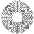
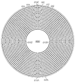
図1を参照すると、研磨パッド10は、円形溝12と半径方向溝16との組み合わせを含む。平坦な、一般には多孔性のランドエリア14が円形溝12及び半径方向溝16を分けている。研磨中、円形溝12が半径方向溝16と組み合わさって、研磨スラリー又は研磨溶液をランドエリア14に分配して、基材、たとえば半導体基材、光学基材又は磁性基材の少なくとも一つと相互作用させる。円形溝12及び半径方向溝16は均一な断面を有する。これらの溝パターンに伴う問題は、時間とともに、研磨くずが溝12及び16中に集まり、その後、定期的にランドエリア14に移動し、そこで欠陥、たとえば基材のスクラッチ欠陥を付与するということである。
Referring to FIG. 1, the
図2を参照すると、研磨パッド200は、すべて半径方向排流溝216に流れ込むことができる供給溝202A、204A、206A、208A及び202B、204B、206B、208Bを含む。この実施形態において、半径方向排流溝216は、供給溝の深さに等しい深さ「D」を有する。研磨中、供給溝202A、204A、206A、208A及び202B、204B、206B、208Bならびに半径方向排流溝216は、研磨スラリー又は溶液をランドエリア214上に分配する。矢印が、研磨パッド200の周壁234に達し、それを通り過ぎる研磨スラリー又は溶液の流れを示す。右回り研磨中、供給溝202A、204A、206A及び208Aからの流れは、供給溝202B、204B、206B及び208Bからの流れよりも大きい。左回り研磨中、供給溝202B、204B、206B及び208Bからの流れは供給溝202A、204A、206A及び208Aからの流れよりも大きい。この任意選択の実施形態は、すべての研磨くずが邪魔されずに半径方向排流溝216を通って研磨パッド200から出ることを許す。
Referring to FIG. 2, the
図2Aを参照すると、研磨パッド200は、すべて半径方向排流溝216に流れ込むことができる供給溝202A、204A、206A及び202B、204B、206Bを含む。この実施形態において、半径方向排流溝216は、供給溝の深さ又は側壁232の高さに等しい深さ「D」を有する。研磨中、供給溝202A、204A、206A及び202B、204B、206Bならびに半径方向排流溝216は、研磨スラリー又は溶液をランドエリア214上に分配する。排流溝216から、研磨スラリー又は溶液は周縁溝210A及び210Bを通って流れる。そして、研磨スラリー又は溶液は、周縁溝210A及び210Bから出て周縁ランドエリア220を乗り越え、周壁222を通り過ぎる。矢印が、周縁溝210A及び210Bに達し、周縁ランドエリア220を乗り越え、研磨パッド200の周壁222を通り過ぎる研磨スラリー又は溶液の流れを示す。右回り研磨中、供給溝202A、204A及び206Aからの流れは供給溝202B、204B及び206Bからの流れよりも大きい。左回り研磨中、供給溝202B、204B及び206Bからの流れは供給溝202A、204A及び206Aからの流れよりも大きい。この任意選択の実施形態は、研磨スラリー又は溶液の排出を遅らせ、いくつかの研磨組み合わせの場合、研磨効率を高めることができる。
Referring to FIG. 2A, the
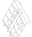
図3を参照すると、研磨パッド300は、すべて半径方向排流溝316に流れ込むことができる供給溝302A、304A、306A、308A及び302B、304B、306B、308Bを含む。この実施形態において、半径方向排流溝316は、供給溝302A、304A、306A、308A及び302B、304B、306B、308Bの深さD1よりも大きい深さ「D」を有する。特に、排流溝316は、供給溝302A、304A、306A、308A及び302B、304B、306B、308Bの深さD1の下にさらなる深さD2だけ延びている。側壁332の高さは深さD1+深さD2に等しい。研磨中、供給溝302A、304A、306A、308A及び302B、304B、306B、308Bならびに半径方向排流溝316は、研磨スラリー又は溶液をランドエリア314上に分配する。矢印が、研磨パッド300の周壁334に達し、それを通り過ぎる研磨スラリー又は溶液の流れを示す。右回り研磨中、供給溝302A、304A及び308Aからの流れは供給溝302B、304B、306B及び308Bからの流れよりも大きい。左回り研磨中、供給溝302B、304B、306B及び308Bからの流れは供給溝302A、304A及び308Aからの流れよりも大きい。この任意選択の実施形態は、すべての研磨くずが邪魔されずに半径方向排流溝316を通って研磨パッド300から出ることを許す。
Referring to FIG. 3, the
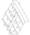
図3Aを参照すると、研磨パッド300は、すべて半径方向排流溝316に流れ込むことができる供給溝302A、304A、306A及び302B、304B、306Bを含む。この実施形態において、半径方向排流溝316は、供給溝302A、304A、306A、308A及び302B、304B、306B、308Bの深さD1よりも大きい深さ「D」を有する。特に、排流溝316は、供給溝302A、304A、306A、308A及び302B、304B、306B、308Bの深さD1の下にさらなる深さD2だけ延びている。この設計は、周縁ランドエリア320を乗り越えて研磨パッド300の周壁322に達する高密度研磨くずの流れを促進する。研磨中、供給溝302A、304A、306A及び302B、304B、306Bならびに半径方向排流溝316は、研磨スラリー又は溶液をランドエリア314上に分配する。排流溝316から、研磨スラリー又は溶液は周縁溝310A及び310Bを通って流れる。そして、研磨スラリー又は溶液は、周縁溝310A及び310Bから出て周縁ランドエリア320を乗り越え、周壁322を通り過ぎる。矢印が、周縁溝310A及び310Bに達し、周縁ランドエリア320を乗り越え、研磨パッド300の周壁322を通り過ぎる研磨スラリー又は溶液の流れを示す。右回り研磨中、供給溝302A、304A及び306Aからの流れは供給溝302B、304B及び306Bからの流れよりも大きい。左回り研磨中、供給溝302B、304B及び306Bからの流れは供給溝302A、304A及び306Aからの流れよりも大きい。この任意選択の実施形態は、研磨スラリー又は溶液の排出を遅らせ、いくつかの研磨組み合わせの場合、研磨効率を高めることができる。
Referring to FIG. 3A, the
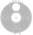
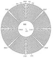
図4を参照すると、研磨パッド400は中心401及び周縁405を有し、半径rが中心401から周縁405まで延びている。この実施形態においては、ウェーハ440が、平行な線で印されたウェーハトラックの周りかつ一つの半径方向排流溝416の上で、研磨パッド400に対して動く。図4は、複数の供給溝412及びランドエリア414を覆うウェーハを示す。半径方向排流溝416は、ウェーハトラックの中及びウェーハトラックの外のすべての供給溝から流れを抜く。
Referring to FIG. 4, the
図5を参照すると、研磨パッド500は、平行な線で印されたウェーハトラックの周りかつ180°離れた二つの半径方向排流溝516A及び516Bの上で、研磨パッド500に対して動くウェーハ540を示す。図5は、複数の供給溝512及びランドエリア514を覆うウェーハを示す。特に、半径方向排流溝516は、研磨トラックを通過して延びて、研磨パッド500の回転中、研磨くずを、ウェーハの下で、研磨トラックに通し、研磨トラックを越えさせて研磨パッド500の周縁505へと除去することを促進する。半径方向排流溝516A及び516Bは、ウェーハトラックの中及びウェーハトラックの外のすべての供給溝から流れを抜く。
Referring to FIG. 5, the
図6を参照すると、研磨パッド600は、90°離れた四つの半径方向排流溝616A〜616Bを示す。あるいはまた、半径方向排流溝及び供給溝の間隔は均等でなくてもよい。動作中、研磨スラリー又は溶液は、ランドエリア614を乗り越え、半径方向排流溝616A〜616Dを通って周縁605に向かって外向きに流れる。半径方向排流溝616A〜616Dは、ウェーハトラック(図示せず)の中及びウェーハトラックの外のすべての供給溝612から流れを抜く。
Referring to FIG. 6, the
図6Aを参照すると、研磨パッド600は、90°離れた四つの半径方向排流溝616A〜616Bを示す。あるいはまた、半径方向排流溝及び供給溝の間隔は均等でなくてもよい。動作中、研磨スラリー又は溶液は、ランドエリア614を乗り越え、半径方向排流溝616A〜616Dを通って周縁605に向かって外向きに流れる。研磨スラリー又は溶液は、周縁605に達する前に、周縁溝610に流れ込み、周縁溝610から周縁ランドエリア620を乗り越えて流れる。半径方向排流溝616A〜616Dは、ウェーハトラック(図示せず)の中及びウェーハトラックの外のすべての供給溝612から流れを抜く。
Referring to FIG. 6A, the
図7を参照すると、研磨パッド700は、45°離れた八つの半径方向排流溝716A〜716Hを示す。あるいはまた、半径方向排流溝及び供給溝の間隔は均等でなくてもよい。動作中、研磨スラリー又は溶液は、ランドエリア714を乗り越え、半径方向排流溝716A〜716Hを通って周縁705に向かって外向きに流れる。半径方向排流溝716A〜716Hは、ウェーハトラック(図示せず)の中及びウェーハトラックの外のすべての供給溝712から流れを抜く。
Referring to FIG. 7, polishing
図8を参照すると、研磨パッド800は、22.5°離れた16本の半径方向排流溝916A〜916Pを示す。あるいはまた、半径方向排流溝及び供給溝の間隔は均等でなくてもよい。動作中、研磨スラリー又は溶液は、ランドエリア814を乗り越え、半径方向排流溝816A〜816Pを通って周縁805に向かって外向きに流れる。半径方向排流溝816A〜816Pは、ウェーハトラック(図示せず)の中及びウェーハトラックの外のすべての供給溝812から流れを抜く。
Referring to FIG. 8, the
図9を参照すると、研磨パッド900は、45°離れた八つのテーパ状の半径方向排流溝916A〜916Hを示す。あるいはまた、半径方向排流溝及び供給溝の間隔は均等でなくてもよい。動作中、研磨スラリー又は溶液は、ランドエリア914を乗り越え、テーパ状の半径方向排流溝916A〜916Hを通って周縁905に向かって外向きに流れる。テーパ状の半径方向排流溝916A〜916Hはすべて、中心901よりも周縁905に向かって大きい幅を有する。このテーパが、半径方向排流溝が増量した流体及び研磨くずの負担を受け入れることを可能にする。幅の代わりに、周縁に向かって深さを増大させて流量を増すこともできる。しかし、大部分の状況の場合、研磨スラリー又は溶液がパッドの周縁に向かって流れるとき、排流溝を通過する流量の増大を受け入れるには、遠心力の増大で十分である。
Referring to FIG. 9, the
本発明に関し、供給溝(δ)は平均供給断面積(δa)を有し、平均供給断面積(δa)は、各供給溝の合計断面積を供給溝(δ)の総数で割ったものである。半径方向排流溝(ρ)は平均排流断面積(ρa)を有し、半径方向排流溝の平均排流断面積(ρa)は、次式にしたがって、平均供給断面積(δa)の少なくとも2倍かつ供給断面積(δa)の8倍未満の大きさである。
2*δa≦ρa≦8*δa
式中、(nr)は半径方向溝の数を表し、(nf)は供給溝の数を表し、次式にしたがって、半径方向排流溝の各側からの合計を表す。
(0.15)nf*δa≦nr*ρa≦(0.35)nf*δa
一般に、nr*は1〜16である。もっとも好都合には、nrは2〜12である。
The present invention relates, the supply grooves ([delta]) has an average supply cross-sectional area of ([delta] a), the average supply cross-sectional area ([delta] a) is divided by the total cross-sectional area of each feed channel by the total number of the feed channels ([delta]) Is. Radial Hairyumizo ([rho) has an average drainage cross section of the ([rho a), average drainage sectional area of the radial drainage grooves ([rho a), according to the following equation, the average supply cross-sectional area ([delta] a ) at least twice as large as the supply cross-sectional area (δ a ).
2 * δ a ≦ ρ a ≦ 8 * δ a
Where (n r ) represents the number of radial grooves, (n f ) represents the number of supply grooves, and represents the sum from each side of the radial drain grooves according to the following equation:
(0.15) n f * δ a ≦ n r * ρ a ≦ (0.35) n f * δ a
In general, n r * is 1-16. Most conveniently, n r is 2-12.
半径方向排流溝の数が増える(1、2、4、8及び16本)一連の研磨パッドが、一定の供給溝面積での排流能力増大を生じさせた。研磨パッドは次のような溝寸法を有するものであった。 A series of polishing pads with increasing number of radial drain grooves (1, 2, 4, 8, and 16) resulted in increased drain capacity with a constant feed groove area. The polishing pad had the following groove dimensions.
一つの円形供給溝の断面積:0.039cm2 Cross-sectional area of one circular supply groove: 0.039 cm 2
排流溝によって二分される供給溝の数:80 Number of supply grooves bisected by drainage grooves: 80
一つの排流溝に供給する供給溝の合計断面積:=0.0039*80*2=0.624cm2
注:本明細書において使用される供給溝計算は、スラリーが供給溝と排流溝との間の各一つの交点の両側から流れるものと仮定する。たとえば、80本の円形供給溝は一つの排流溝とで160の溝交点を形成する。
一つの排流溝の断面積:0.01741932cm2
Total cross-sectional area of the supply groove to be supplied to one drainage groove: = 0.0039 * 80 * 2 = 0.624 cm 2
Note: The feed groove calculations used herein assume that the slurry flows from both sides of each one intersection between the feed and drain grooves. For example, 80 circular supply grooves form 160 groove intersections with one discharge groove.
Cross-sectional area of one drainage groove: 0.01741932 cm 2
一つの排流溝が適用された場合の供給溝断面積に対する半径方向排流溝断面積の比:0.03 Ratio of radial drain groove cross-sectional area to supply groove cross-sectional area when one drain groove is applied: 0.03
この実施例においては、一連の供給溝から効果的に流れを抜くのに一つの排流溝では不十分であった。しかし、複数の供給溝の付加により、排流効率を許容可能なレベルまで容易に高めることができる。図10は、溝の数とともに改善された排流能力が高まることをグラフで示す。 In this embodiment, one drain groove was not sufficient to effectively drain the flow from the series of supply grooves. However, the addition of a plurality of supply grooves can easily increase the drainage efficiency to an acceptable level. FIG. 10 graphically shows that the improved drainage capability increases with the number of grooves.
0.15未満の相対排流面積比は効果がない。パッドの上面への新鮮なスラリーの過剰な送り出しのせいで、半径方向溝の数は、スラリー送り出し速度を含むいくつかの変数に依存する。排流能力が高すぎるならば、これは、溝の中で利用可能なスラリーを不十分にしてしまい、結果的にパッドの乾燥を生じさせるおそれがある。これが、スクラッチ欠陥のような欠陥の有害な発生源である。本発明の排流溝は欠陥を減らす。同様に、低すぎる排流比は、十分な研磨副生成物を除去せず、欠陥を減らさない。高すぎる排流比は、流体力学に影響を及ぼし(ウェーハ不均一性の増大によって示される)、排流溝が用いられない場合よりも欠陥を増加させた。 A relative drainage area ratio of less than 0.15 has no effect. Due to excessive delivery of fresh slurry to the top surface of the pad, the number of radial grooves depends on several variables including the slurry delivery rate. If the drainage capacity is too high, this can result in insufficient slurry available in the grooves, resulting in pad drying. This is a harmful source of defects such as scratch defects. The drainage groove of the present invention reduces defects. Similarly, a drainage ratio that is too low will not remove enough polishing by-products and will not reduce defects. Too high drainage ratios affected hydrodynamics (indicated by increased wafer non-uniformity) and increased defects than if drainage grooves were not used.
最適範囲を評価するために、以下の実験を実施した。五つの異なる半径方向溝を一連の独立気泡ポリウレタン研磨パッドに適用した。これらのパッドは、幅20mil、深さ30mil及びピッチ120mil(0.051cm×0.076cm×ピッチ0.305cm)の円形溝を有するものであった。呼称ならびに半径方向溝の寸法及び数を表1に示す。 In order to evaluate the optimal range, the following experiment was conducted. Five different radial grooves were applied to a series of closed cell polyurethane polishing pads. These pads had circular grooves with a width of 20 mils, a depth of 30 mils, and a pitch of 120 mils (0.051 cm × 0.076 cm × pitch 0.305 cm). Nomenclature and dimensions and number of radial grooves are shown in Table 1.

研磨条件は以下のように要約される。
MDC Mirra、K1505-50μmコロイダルスラリー
Saesol AK45(8031cl)ダイアモンドディスク、パッドならし30分7psi(48kPa)、全インサイチュー条件7psi(48kPa)
プロセス:パッドダウンフォース3psi(20.7kPa)
プラテン速度93rpm
キャリヤ速度87rpm
スラリー流量200ml/m
11、37、63、89、115、141、167及び193のウェーハカウントで研磨されたウェーハをモニタ。
KLA-TencorからのSurfscan SP1アナライザを用いて欠陥カウントを実施。
The polishing conditions are summarized as follows.
MDC Mirra, K1505-50μm colloidal slurry
Saesol AK45 (8031cl) diamond disc, pad leveling 30min 7psi (48kPa), all in situ conditions 7psi (48kPa)
Process: Pad down force 3psi (20.7kPa)
Platen speed 93rpm
Carrier speed 87rpm
Slurry flow rate 200ml / m
Monitors polished wafers with 11, 37, 63, 89, 115, 141, 167 and 193 wafer counts.
Defect counts are performed using the Surfscan SP1 analyzer from KLA-Tencor.
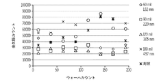
各パッドをならし運用して始動効果を排除し、200個のウェーハを研磨して速度及び欠陥率安定性を評価した。パッド間の速度に大きな差はなかった。しかし、図11及び12に示すように、欠陥率に有意な差があった。幅90mil(0.229cm)/8半径方向溝及び幅120mil(0.305cm)/8半径方向溝のパッドサンプルが、低く安定した欠陥レベルを示した。対照を含む他すべては、試験の期間とともに変化し、研磨時間の増大とともに増大する、より高い欠陥レベルを示した。これは、対照パッドの挙動を90mil(0.229cm)溝パッドと比較した図11で特に明らかである。 Each pad was operated to eliminate the starting effect, and 200 wafers were polished to evaluate the speed and defect rate stability. There was no significant difference in speed between pads. However, as shown in FIGS. 11 and 12, there was a significant difference in the defect rate. Pad samples of 90 mil (0.229 cm) / 8 radial groove and 120 mil (0.305 cm) / 8 radial groove showed low and stable defect levels. All others, including the control, showed higher defect levels that varied with the duration of the test and increased with increasing polishing time. This is particularly evident in FIG. 11 where the control pad behavior is compared to a 90 mil (0.229 cm) groove pad.
排流溝の数の倍増(供給溝に対する排流溝の面積比が0.225から0.45に増大)は、対照と比べてさえ、全体欠陥率を有意に増大させた。これは、排流効率比にとって決定的な範囲があるという暗示と考えられる。この決定的な範囲は、供給溝のサイズ及び数ならびに半径方向排流溝のサイズとともに変化することができる。 A doubling of the number of drain grooves (the ratio of drain grooves to feed grooves increased from 0.225 to 0.45) significantly increased the overall defect rate even compared to the control. This is thought to be an indication that there is a critical range for the exhaust efficiency ratio. This critical range can vary with the size and number of feed grooves and the size of the radial drain grooves.
また、HFエッチング後の欠陥データを調べて、全欠陥率をスクラッチ密度と比較した。HFエッチングは、粒子を除去するのに効果的であり、スクラッチに対する感度を高めた。理由は、HFが、クラックそのもの(デコレーション)の周囲のひずみ領域の除去によってスクラッチ深さを拡大するからである。図13に示すように、90mil(0.229cm)/8及び120mil(0.305cm)/8パッドの場合でも同じ低く安定な欠陥応答が認められたが、60mil(0.152cm)/8パッド応答がさらに近似し、そのパッドサンプル中の全欠陥の大きな割合が、大きな損傷性の凝集塊ではなく、小さな粒状物であることを示した。これは、排流効率比には下限もあるという指示である。これらの結果に基づくと、供給溝に対する半径方向排流溝の面積比の決定的範囲0.2〜0.3がもっとも好都合である。 Further, defect data after HF etching was examined, and the total defect rate was compared with the scratch density. HF etching was effective in removing particles and increased sensitivity to scratches. The reason is that HF expands the scratch depth by removing the strain area around the crack itself (decoration). As shown in FIG. 13, the same low and stable defect response was observed in the case of 90 mil (0.229 cm) / 8 and 120 mil (0.305 cm) / 8 pad, but 60 mil (0.152 cm) / 8 pad response. Further approximated, indicating that a large percentage of the total defects in the pad sample were small particulates rather than large damaging agglomerates. This is an indication that the exhaust efficiency ratio also has a lower limit. Based on these results, the definitive range 0.2-0.3 of the area ratio of the radial drain groove to the supply groove is most convenient.
上記から、排流効率式を使用して、広く多様な供給溝寸法及びピッチの場合に欠陥率の低下を達成するために必要な排流溝の寸法及び数を決定することができることが明らかになる。いくつかの現実的な制限が課されることがある。たとえば、一つの排流溝しか用いないことは、回転の偏心のせいで、おそらく望ましくない。また、排流溝は半径方向溝又はその変形に限定されるべきであると結論づけられる。この理由は、a)一つの回転対称を有し、b)テキスチャ由来のナノトポグラフィー(望ましくない)に最小限しか寄与しないからである。また、溝寸法に関して、半径とともに幅が広がるように半径方向排流溝を設計し、パッドの周縁で計算される上記排流効率比の範囲に制限を加えることによって輸送をさらに規制することが望ましいかもしれない。 From the above it is clear that the drainage efficiency equation can be used to determine the size and number of drainage grooves required to achieve a reduced defect rate for a wide variety of supply groove sizes and pitches. Become. Some practical restrictions may be imposed. For example, the use of only one drain groove is probably undesirable due to rotational eccentricity. It is also concluded that the drainage groove should be limited to radial grooves or variations thereof. This is because a) has a single rotational symmetry and b) contributes minimally to texture-derived nanotopography (which is undesirable). In addition, it is desirable to further restrict the transportation by designing the radial drainage groove so that the width increases with the radius with respect to the groove size, and by limiting the range of the drainage efficiency ratio calculated at the periphery of the pad. It may be.
本発明は、低い欠陥レベルを維持する長期的ケミカルメカニカルプラナリゼーション用途のための多孔性研磨パッドを形成するのに効果的である。加えて、これらのパッドは、研磨速度、大域的均一性を改善し、研磨振動を減らすことができる。 The present invention is effective in forming porous polishing pads for long-term chemical mechanical planarization applications that maintain low defect levels. In addition, these pads can improve polishing rate, global uniformity, and reduce polishing vibration.
Claims (10)
ポリマーマトリックス及び厚さを有する研磨層であって、中心、周縁、前記中心から前記周縁まで延びる半径及び前記中心を包囲し、前記半径と交差する研磨トラック(前記半導体基材、光学基材及び磁性基材の少なくとも一つを研磨又は平坦化するための前記研磨層の作用領域を表す)を含む研磨層と;
前記半径と交差する複数の供給溝(δ)であって、前記半導体基材、光学基材及び磁性基材の少なくとも一つを前記研磨パッド及び前記研磨流体で研磨又は平坦化するためのランドエリアを供給溝(δ)の間に有し、平均供給断面積(δa)(各供給溝の合計断面積を供給溝(δ)の総数で割ったもの)を有する複数の供給溝(δ)と;
前記研磨流体が前記複数の供給溝(δ)から少なくとも一つの半径方向排流溝(ρ)に流れることを許すための、前記複数の供給溝(δ)と交差する、前記研磨層中の少なくとも一つの半径方向排流溝(ρ)と、を含み、
前記少なくとも一つの半径方向排流溝(ρ)が平均排流断面積(ρa)を有し、
前記少なくとも一つの半径方向排流溝の前記平均排流断面積(ρa)が、
2*δa≦ρa≦8*δa
(式中、(nr)は半径方向溝の数を表し、(nf)は供給溝の数を表す)
及び
(0.15)nf*δa≦nr*ρa≦(0.35)nf*δa
にしたがって前記平均供給断面積(δa)よりも大きく、
前記少なくとも一つの半径方向排流溝(ρ)が前記研磨トラックを通過して延びて、前記研磨パッドの回転中、研磨くずを、前記半導体基材、光学基材及び磁性基材の少なくとも一つの下で、前記研磨トラックに通し、前記研磨トラックを越えさせて前記研磨パッドの前記周縁へと除去することを促進する、研磨パッド。 Polishing or planarizing at least one of the semiconductor substrate, the optical substrate, and the magnetic substrate by relative movement between the polishing fluid and the polishing pad and at least one of the semiconductor substrate, the optical substrate, and the magnetic substrate. A polishing pad suitable for
A polishing layer having a polymer matrix and a thickness, comprising a center, a periphery, a radius extending from the center to the periphery, and a polishing track surrounding the center and intersecting the radius (the semiconductor substrate, the optical substrate and the magnetic substrate) A polishing layer comprising (representing a working area of the polishing layer for polishing or planarizing at least one of the substrates);
A plurality of supply grooves (δ) intersecting with the radius, and a land area for polishing or flattening at least one of the semiconductor substrate, the optical substrate and the magnetic substrate with the polishing pad and the polishing fluid Between the supply grooves (δ) and a plurality of supply grooves (δ) having an average supply cross-sectional area (δ a ) (the total cross-sectional area of each supply groove divided by the total number of supply grooves (δ)) When;
At least in the polishing layer intersecting the plurality of supply grooves (δ) to allow the polishing fluid to flow from the plurality of supply grooves (δ) to at least one radial drain groove (ρ). One radial drain groove (ρ),
The at least one radial drain groove (ρ) has an average drain cross-sectional area (ρ a );
The mean drain cross section (ρ a ) of the at least one radial drain groove is
2 * δ a ≦ ρ a ≦ 8 * δ a
( Wherein (n r ) represents the number of radial grooves and (n f ) represents the number of supply grooves)
And (0.15) n f * δ a ≦ n r * ρ a ≦ (0.35) n f * δ a
Greater than the average supply cross section (δ a ) according to
The at least one radial drain groove (ρ) extends through the polishing track, and during rotation of the polishing pad, polishing debris is transferred to at least one of the semiconductor substrate, the optical substrate, and the magnetic substrate. A polishing pad that facilitates passing under the polishing track below and over the polishing track to the periphery of the polishing pad.
ポリマーマトリックス及び厚さを有する研磨層であって、中心、周縁、前記中心から前記周縁まで延びる半径及び前記中心を包囲し、前記半径と交差する研磨トラック(前記半導体基材、光学基材及び磁性基材の少なくとも一つを研磨又は平坦化するための前記研磨層の作用領域を表す)を含む研磨層と;
前記半径と交差する複数の供給溝(δ)であって、前記半導体基材、光学基材及び磁性基材の少なくとも一つを前記研磨パッド及び前記研磨流体で研磨又は平坦化するためのランドエリアを供給溝(δ)の間に有し、平均供給断面積(δa)(各供給溝の合計断面積を供給溝(δ)の総数で割ったもの)を有する複数の供給溝(δ)と;
前記研磨流体が前記複数の供給溝(δ)から少なくとも一つの半径方向排流溝(ρ)に流れることを許すための、前記複数の供給溝(δ)と交差する、前記研磨層中の少なくとも一つの半径方向排流溝(ρ)と、を含み、
前記少なくとも一つの半径方向排流溝(ρ)が平均排流断面積(ρa)を有し、前記少なくとも一つの半径方向排流溝の平均排流断面積(ρa)が、
2*δa≦ρa≦8*δa
(式中、(nr)は半径方向溝の数を表し、(nf)は供給溝の数を表す)
及び
(0.15)nf*δa≦nr*ρa≦(0.35)nf*δa
(式中、nrは数2〜12に等しい)
にしたがって前記平均供給断面積(δa)よりも大きく、
前記少なくとも一つの半径方向排流溝(ρ)が前記研磨トラックを通過して延びて、前記研磨パッドの回転中、研磨くずを、前記半導体基材、光学基材及び磁性基材の少なくとも一つの下で、前記研磨トラックに通し、前記研磨トラックを越えさせて前記研磨パッドの前記周縁へと除去することを促進する、研磨パッド。 Polishing or planarizing at least one of the semiconductor substrate, the optical substrate, and the magnetic substrate by relative movement between the polishing fluid and the polishing pad and at least one of the semiconductor substrate, the optical substrate, and the magnetic substrate. A polishing pad suitable for
A polishing layer having a polymer matrix and a thickness, comprising a center, a periphery, a radius extending from the center to the periphery, and a polishing track surrounding the center and intersecting the radius (the semiconductor substrate, the optical substrate and the magnetic substrate) A polishing layer comprising (representing a working area of the polishing layer for polishing or planarizing at least one of the substrates);
A plurality of supply grooves (δ) intersecting with the radius, and a land area for polishing or flattening at least one of the semiconductor substrate, the optical substrate and the magnetic substrate with the polishing pad and the polishing fluid Between the supply grooves (δ) and a plurality of supply grooves (δ) having an average supply cross-sectional area (δ a ) (the total cross-sectional area of each supply groove divided by the total number of supply grooves (δ)) When;
At least in the polishing layer intersecting the plurality of supply grooves (δ) to allow the polishing fluid to flow from the plurality of supply grooves (δ) to at least one radial drain groove (ρ). One radial drain groove (ρ),
It said at least one radial Hairyumizo ([rho) has an average drainage cross section of the ([rho a), the average discharge flow cross-sectional area of the at least one radial drainage grooves ([rho a) is,
2 * δ a ≦ ρ a ≦ 8 * δ a
( Wherein (n r ) represents the number of radial grooves and (n f ) represents the number of supply grooves)
And (0.15) n f * δ a ≦ n r * ρ a ≦ (0.35) n f * δ a
(Where n r is equal to the number 2-12)
Greater than the average supply cross section (δ a ) according to
The at least one radial drain groove (ρ) extends through the polishing track, and during rotation of the polishing pad, polishing debris is transferred to at least one of the semiconductor substrate, the optical substrate, and the magnetic substrate. A polishing pad that facilitates passing under the polishing track below and over the polishing track to the periphery of the polishing pad.
Applications Claiming Priority (2)
| Application Number | Priority Date | Filing Date | Title |
|---|---|---|---|
| US15/079,824 | 2016-03-24 | ||
| US15/079,824 US10875146B2 (en) | 2016-03-24 | 2016-03-24 | Debris-removal groove for CMP polishing pad |
Publications (3)
| Publication Number | Publication Date |
|---|---|
| JP2017208530A true JP2017208530A (en) | 2017-11-24 |
| JP2017208530A5 JP2017208530A5 (en) | 2020-04-16 |
| JP6993090B2 JP6993090B2 (en) | 2022-01-13 |
Family
ID=59886174
Family Applications (1)
| Application Number | Title | Priority Date | Filing Date |
|---|---|---|---|
| JP2017056833A Active JP6993090B2 (en) | 2016-03-24 | 2017-03-23 | Polishing scrap removal groove for CMP polishing pad |
Country Status (6)
| Country | Link |
|---|---|
| US (1) | US10875146B2 (en) |
| JP (1) | JP6993090B2 (en) |
| KR (1) | KR102363154B1 (en) |
| CN (1) | CN107225498A (en) |
| FR (1) | FR3049205B1 (en) |
| TW (1) | TWI773663B (en) |
Cited By (2)
| Publication number | Priority date | Publication date | Assignee | Title |
|---|---|---|---|---|
| JP2019217627A (en) * | 2018-06-21 | 2019-12-26 | エスケイシー・カンパニー・リミテッドSkc Co., Ltd. | Polishing pad with improved fluidity of slurry and process for preparing the same |
| WO2023013576A1 (en) | 2021-08-04 | 2023-02-09 | 株式会社クラレ | Polishing pad |
Families Citing this family (11)
| Publication number | Priority date | Publication date | Assignee | Title |
|---|---|---|---|---|
| DE102017216033A1 (en) * | 2017-09-12 | 2019-03-14 | Carl Zeiss Smt Gmbh | Method for processing a workpiece in the manufacture of an optical element |
| CN108214285A (en) * | 2018-01-25 | 2018-06-29 | 成都时代立夫科技有限公司 | A kind of chemical mechanical polishing pads |
| JP7026942B2 (en) * | 2018-04-26 | 2022-03-01 | 丸石産業株式会社 | Underlay for polishing pad and polishing method using the underlay |
| KR101952829B1 (en) * | 2018-08-13 | 2019-02-27 | 최유섭 | Polishing apparatus for metal part and polishing method using the same |
| JP7178662B2 (en) * | 2019-04-10 | 2022-11-28 | パナソニックIpマネジメント株式会社 | Polishing device and polishing method |
| TWI771668B (en) | 2019-04-18 | 2022-07-21 | 美商應用材料股份有限公司 | Temperature-based in-situ edge assymetry correction during cmp |
| CN110732983A (en) * | 2019-10-30 | 2020-01-31 | 郑州伯利森新材料科技有限公司 | Repair-free superhard grinding wheel for processing hard and brittle materials and preparation method thereof |
| TWI826280B (en) * | 2019-11-22 | 2023-12-11 | 美商應用材料股份有限公司 | Wafer edge asymmetry correction using groove in polishing pad |
| KR20210116759A (en) | 2020-03-13 | 2021-09-28 | 삼성전자주식회사 | CMP pad and chemical mechanical polishing apparatus having the same |
| US20210299816A1 (en) * | 2020-03-25 | 2021-09-30 | Rohm And Haas Electronic Materials Cmp Holdings, Inc. | Cmp polishing pad with protruding structures having engineered open void space |
| KR102570825B1 (en) * | 2020-07-16 | 2023-08-28 | 한국생산기술연구원 | Polishing pad including porous protruding pattern and polishing apparatus including the same |
Citations (3)
| Publication number | Priority date | Publication date | Assignee | Title |
|---|---|---|---|---|
| JP2006156876A (en) * | 2004-12-01 | 2006-06-15 | Toyo Tire & Rubber Co Ltd | Polishing pad, polishing method, semiconductor device and manufacturing method thereof |
| JP2007081322A (en) * | 2005-09-16 | 2007-03-29 | Jsr Corp | Method for manufacturing chemical-mechanical polishing pad |
| US20090311955A1 (en) * | 2008-03-14 | 2009-12-17 | Nexplanar Corporation | Grooved CMP pad |
Family Cites Families (24)
| Publication number | Priority date | Publication date | Assignee | Title |
|---|---|---|---|---|
| MY114512A (en) | 1992-08-19 | 2002-11-30 | Rodel Inc | Polymeric substrate with polymeric microelements |
| US5645469A (en) | 1996-09-06 | 1997-07-08 | Advanced Micro Devices, Inc. | Polishing pad with radially extending tapered channels |
| JPH11156699A (en) | 1997-11-25 | 1999-06-15 | Speedfam Co Ltd | Surface polishing pad |
| US6135868A (en) * | 1998-02-11 | 2000-10-24 | Applied Materials, Inc. | Groove cleaning device for chemical-mechanical polishing |
| GB2345255B (en) | 1998-12-29 | 2000-12-27 | United Microelectronics Corp | Chemical-Mechanical Polishing Pad |
| KR100471527B1 (en) * | 1999-03-30 | 2005-03-09 | 가부시키가이샤 니콘 | Polishing body, polisher, polishing method, and method for producing semiconductor device |
| US7004823B2 (en) * | 2000-06-19 | 2006-02-28 | Struers A/S | Multi-zone grinding and/or polishing sheet |
| US20040014413A1 (en) * | 2002-06-03 | 2004-01-22 | Jsr Corporation | Polishing pad and multi-layer polishing pad |
| US6843711B1 (en) * | 2003-12-11 | 2005-01-18 | Rohm And Haas Electronic Materials Cmp Holdings, Inc | Chemical mechanical polishing pad having a process-dependent groove configuration |
| JP4645825B2 (en) | 2004-05-20 | 2011-03-09 | Jsr株式会社 | Chemical mechanical polishing pad and chemical mechanical polishing method |
| US7329174B2 (en) | 2004-05-20 | 2008-02-12 | Jsr Corporation | Method of manufacturing chemical mechanical polishing pad |
| KR101279819B1 (en) * | 2005-04-12 | 2013-06-28 | 롬 앤드 하스 일렉트로닉 머티리얼스 씨엠피 홀딩스 인코포레이티드 | Radial-biased polishing pad |
| JP2009220265A (en) * | 2008-02-18 | 2009-10-01 | Jsr Corp | Chemical machinery polishing pad |
| EP2444433A4 (en) * | 2009-06-18 | 2014-06-11 | Jsr Corp | Polyurethane, composition for formation of polishing layers that contains same, pad for chemical mechanical polishing, and chemical mechanical polishing method using same |
| CN102498549A (en) * | 2009-07-16 | 2012-06-13 | 嘉柏微电子材料股份公司 | Grooved cmp polishing pad |
| KR20110100080A (en) * | 2010-03-03 | 2011-09-09 | 삼성전자주식회사 | Polishing pad for chemical mechanical polishing process and chemical mechanical polishing apparatus having the same |
| JP2012106328A (en) * | 2010-03-25 | 2012-06-07 | Toyo Tire & Rubber Co Ltd | Laminate polishing pad |
| KR101232787B1 (en) * | 2010-08-18 | 2013-02-13 | 주식회사 엘지화학 | Polishing-Pad for polishing system |
| US9211628B2 (en) * | 2011-01-26 | 2015-12-15 | Nexplanar Corporation | Polishing pad with concentric or approximately concentric polygon groove pattern |
| US8968058B2 (en) * | 2011-05-05 | 2015-03-03 | Nexplanar Corporation | Polishing pad with alignment feature |
| WO2013039181A1 (en) * | 2011-09-15 | 2013-03-21 | 東レ株式会社 | Polishing pad |
| JPWO2013103142A1 (en) | 2012-01-06 | 2015-05-11 | 東レ株式会社 | Polishing pad |
| TWI599447B (en) * | 2013-10-18 | 2017-09-21 | 卡博特微電子公司 | Cmp polishing pad having edge exclusion region of offset concentric groove pattern |
| JP2016124043A (en) | 2014-12-26 | 2016-07-11 | 東洋ゴム工業株式会社 | Abrasive pad |
-
2016
- 2016-03-24 US US15/079,824 patent/US10875146B2/en active Active
-
2017
- 2017-03-23 CN CN201710180712.XA patent/CN107225498A/en active Pending
- 2017-03-23 JP JP2017056833A patent/JP6993090B2/en active Active
- 2017-03-23 KR KR1020170036719A patent/KR102363154B1/en active IP Right Grant
- 2017-03-23 TW TW106109816A patent/TWI773663B/en active
- 2017-03-24 FR FR1752492A patent/FR3049205B1/en active Active
Patent Citations (3)
| Publication number | Priority date | Publication date | Assignee | Title |
|---|---|---|---|---|
| JP2006156876A (en) * | 2004-12-01 | 2006-06-15 | Toyo Tire & Rubber Co Ltd | Polishing pad, polishing method, semiconductor device and manufacturing method thereof |
| JP2007081322A (en) * | 2005-09-16 | 2007-03-29 | Jsr Corp | Method for manufacturing chemical-mechanical polishing pad |
| US20090311955A1 (en) * | 2008-03-14 | 2009-12-17 | Nexplanar Corporation | Grooved CMP pad |
Cited By (3)
| Publication number | Priority date | Publication date | Assignee | Title |
|---|---|---|---|---|
| JP2019217627A (en) * | 2018-06-21 | 2019-12-26 | エスケイシー・カンパニー・リミテッドSkc Co., Ltd. | Polishing pad with improved fluidity of slurry and process for preparing the same |
| WO2023013576A1 (en) | 2021-08-04 | 2023-02-09 | 株式会社クラレ | Polishing pad |
| KR20240034874A (en) | 2021-08-04 | 2024-03-14 | 주식회사 쿠라레 | polishing pad |
Also Published As
| Publication number | Publication date |
|---|---|
| CN107225498A (en) | 2017-10-03 |
| FR3049205B1 (en) | 2021-08-06 |
| FR3049205A1 (en) | 2017-09-29 |
| TWI773663B (en) | 2022-08-11 |
| KR102363154B1 (en) | 2022-02-15 |
| US10875146B2 (en) | 2020-12-29 |
| US20170274496A1 (en) | 2017-09-28 |
| JP6993090B2 (en) | 2022-01-13 |
| TW201800181A (en) | 2018-01-01 |
| KR20170113203A (en) | 2017-10-12 |
Similar Documents
| Publication | Publication Date | Title |
|---|---|---|
| JP2017208530A (en) | Debris-removal groove for cmp polishing pad | |
| KR100471527B1 (en) | Polishing body, polisher, polishing method, and method for producing semiconductor device | |
| EP0907460B1 (en) | Method for chemical-mechanical planarization of stop-on-feature semiconductor wafers | |
| KR101184628B1 (en) | Polishing pad having grooves configured to promote mixing wakes during polishing | |
| JP4689240B2 (en) | Polishing pad having groove structure for reducing slurry consumption | |
| US6955587B2 (en) | Grooved polishing pad and method | |
| JP5968365B2 (en) | Semiconductor wafer double-side polishing method | |
| SG177625A1 (en) | Grooved cmp polishing pad | |
| US20100159810A1 (en) | High-rate polishing method | |
| US6949012B2 (en) | Polishing pad conditioning method and apparatus | |
| US7070480B2 (en) | Method and apparatus for polishing substrates | |
| JP2004243518A (en) | Polishing device | |
| JP4689241B2 (en) | Polishing pad with grooves to increase slurry utilization | |
| JP3788810B2 (en) | Polishing equipment | |
| US6899612B2 (en) | Polishing pad apparatus and methods | |
| CN101116953A (en) | Chemical mechanism grinding and finishing device | |
| CN114952609A (en) | CMP polishing pad with controllable content ratio of new polishing solution and old polishing solution, polishing method and application thereof | |
| JP4449905B2 (en) | Polishing cloth, polishing cloth processing method, and substrate manufacturing method using the same | |
| KR101455919B1 (en) | Structure of Lapping Plate in Double Side Lapping Apparatus For Silicon Wafer | |
| JP2865250B1 (en) | Method for manufacturing silicon semiconductor wafer | |
| Ishizuka et al. | PCD Dressers for Chemical Mechanical Planarization with Uniform Polishing |
Legal Events
| Date | Code | Title | Description |
|---|---|---|---|
| A521 | Request for written amendment filed |
Free format text: JAPANESE INTERMEDIATE CODE: A523 Effective date: 20200309 |
|
| A621 | Written request for application examination |
Free format text: JAPANESE INTERMEDIATE CODE: A621 Effective date: 20200309 |
|
| A977 | Report on retrieval |
Free format text: JAPANESE INTERMEDIATE CODE: A971007 Effective date: 20210415 |
|
| A131 | Notification of reasons for refusal |
Free format text: JAPANESE INTERMEDIATE CODE: A131 Effective date: 20210608 |
|
| A601 | Written request for extension of time |
Free format text: JAPANESE INTERMEDIATE CODE: A601 Effective date: 20210903 |
|
| A521 | Request for written amendment filed |
Free format text: JAPANESE INTERMEDIATE CODE: A523 Effective date: 20211029 |
|
| TRDD | Decision of grant or rejection written | ||
| A01 | Written decision to grant a patent or to grant a registration (utility model) |
Free format text: JAPANESE INTERMEDIATE CODE: A01 Effective date: 20211116 |
|
| A61 | First payment of annual fees (during grant procedure) |
Free format text: JAPANESE INTERMEDIATE CODE: A61 Effective date: 20211209 |
|
| R150 | Certificate of patent or registration of utility model |
Ref document number: 6993090 Country of ref document: JP Free format text: JAPANESE INTERMEDIATE CODE: R150 |
|
| R157 | Certificate of patent or utility model (correction) |
Free format text: JAPANESE INTERMEDIATE CODE: R157 |