以下に、本発明に係る実施形態を図面に基づいて詳細に説明する。なお、この実施形態によりこの発明が限定されるものではない。また、下記実施形態における構成要素には、当業者が置換可能かつ容易なもの、あるいは実質的に同一のものが含まれる。
Embodiments according to the present invention will be described below in detail with reference to the drawings. In addition, this invention is not limited by this embodiment. In addition, constituent elements in the following embodiments include those that can be easily replaced by those skilled in the art or those that are substantially the same.
[実施形態1]
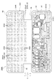
本実施形態に係る回路基板製造方法は、図1等に示す回路基板1を製造するものである。以下では、まず、回路基板1の基本的な構成について説明し、その後、回路基板製造方法について詳細に説明する。図1に示す本実施形態に係る回路基板1は、種々の電子部品2が実装され、これらを電気的に接続する電子回路を構成するものであり、いわゆるプリント回路基板(Printed Circuit Board)である。回路基板1は、種々の形状の電子部品ユニット(例えば、図8に示す電子部品ユニット100等)に適用可能なものである。本実施形態の回路基板1は、典型的には、電子部品2が実装されていない部分だけでなく電子部品2が実装される部分にも相対的に可撓性が高い部分を含むことで好適に種々の形状に追従可能とする共に当該種々の形状に追従可能とする構成を安価に実現するものであり、これにより、適正に形状追従性の確保を図ったものである。なお、相対的に可撓性が高い部分とは、典型的には、相対的に可撓性が低い他の部位と比較して相対的に屈曲しやすい部分である。以下、各図を参照して回路基板1の各構成について詳細に説明する。
[Embodiment 1]
The circuit board manufacturing method according to the present embodiment manufactures the circuit board 1 shown in FIG. In the following, first, the basic configuration of the circuit board 1 will be described, and then the circuit board manufacturing method will be described in detail. A circuit board 1 according to this embodiment shown in FIG. 1 constitutes an electronic circuit on which various electronic components 2 are mounted and electrically connect them, and is a so-called printed circuit board. . The circuit board 1 is applicable to electronic component units having various shapes (for example, the electronic component unit 100 shown in FIG. 8). The circuit board 1 according to the present embodiment is typically suitable by including a portion having relatively high flexibility not only in a portion where the electronic component 2 is not mounted but also in a portion where the electronic component 2 is mounted. In addition, a configuration capable of following various shapes and capable of following the various shapes is realized at low cost, thereby ensuring shape followability appropriately. Note that the portion having relatively high flexibility is typically a portion that is relatively easily bent as compared with other portions having relatively low flexibility. Hereafter, each structure of the circuit board 1 is demonstrated in detail with reference to each figure.
具体的には、本実施形態の回路基板1は、図1、図2に示すように、複数の電子部品2と、第1実装部3と、第2実装部4とを備え、複数の電子部品2が第1実装部3、第2実装部4に実装されることで電子回路を構成する。本実施形態の回路基板1は、第1実装部3がリジッド部を構成し第2実装部4がフレキシブル部を構成することで、いわゆるリジッドフレキシブルプリント回路基板(Rigid Flexible Printed Circuit Board)を構成する。
Specifically, as shown in FIGS. 1 and 2, the circuit board 1 of the present embodiment includes a plurality of electronic components 2, a first mounting unit 3, and a second mounting unit 4, and includes a plurality of electronic components. The component 2 is mounted on the first mounting unit 3 and the second mounting unit 4 to constitute an electronic circuit. The circuit board 1 of the present embodiment constitutes a so-called rigid flexible printed circuit board, with the first mounting part 3 constituting a rigid part and the second mounting part 4 constituting a flexible part. .
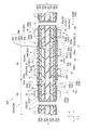
なお、以下では、説明を分かり易くするために、便宜的に互いに交差する第1方向、第2方向、及び、第3方向のうち、第1方向を「積層方向X」といい、第2方向を「短辺方向Y」といい、第3方向を「長辺方向Z」という。典型的には、第1方向としての積層方向Xと第2方向としての短辺方向Yと第3方向としての長辺方向Zとは、相互に直交する。ここでは、積層方向Xは、回路基板1が屈曲していない略板状の状態で、後述する第1実装部3、第2実装部4の絶縁層32、42の厚み方向でかつ当該複数の絶縁層32が積層される方向に相当する。また、短辺方向Y、及び、長辺方向Zは、回路基板1が屈曲していない略板状の状態で、絶縁層32、42の延在方向に相当する。このうち短辺方向Yは、第1実装部3と第2実装部4とが隣接する方向に相当する。以下の説明で用いる各方向は、特に断りのない限り、回路基板1が屈曲していない略板状の状態、すなわち、第1実装部3に対して第2実装部4が屈曲していない状態での方向として説明する。
In the following, for the sake of easy understanding, the first direction is referred to as “stacking direction X” among the first direction, the second direction, and the third direction that intersect with each other for convenience, and the second direction Is referred to as “short side direction Y”, and the third direction is referred to as “long side direction Z”. Typically, the stacking direction X as the first direction, the short side direction Y as the second direction, and the long side direction Z as the third direction are orthogonal to each other. Here, the stacking direction X is a substantially plate-like state in which the circuit board 1 is not bent, and is in the thickness direction of the insulating layers 32 and 42 of the first mounting portion 3 and the second mounting portion 4 to be described later, This corresponds to the direction in which the insulating layer 32 is laminated. The short side direction Y and the long side direction Z correspond to the extending direction of the insulating layers 32 and 42 in a substantially plate-like state in which the circuit board 1 is not bent. Among these, the short side direction Y corresponds to a direction in which the first mounting unit 3 and the second mounting unit 4 are adjacent to each other. Unless otherwise specified, each direction used in the following description is a substantially plate-like state in which the circuit board 1 is not bent, that is, a state in which the second mounting portion 4 is not bent with respect to the first mounting portion 3. This will be described as the direction.
電子部品2は、第1実装部3、第2実装部4に実装されるものであり、各種機能を発揮するための種々の素子である。電子部品2は、一例として、コネクタ、ヒューズ、リレー、コンデンサ、抵抗、トランジスタ、IPS(Intelligent Power Switch)、分岐部、ECU(Electronic Control Unit)・マイコン等を含む電子制御ユニット、各種センサ素子、LED(Light Emitting Diode)素子、スピーカ等である。
The electronic component 2 is mounted on the first mounting portion 3 and the second mounting portion 4 and is various elements for exhibiting various functions. As an example, the electronic component 2 includes a connector, a fuse, a relay, a capacitor, a resistor, a transistor, an IPS (Intelligent Power Switch), a branching unit, an electronic control unit including an ECU (Electronic Control Unit) / microcomputer, various sensor elements, LEDs (Light Emitting Diode) elements, speakers, and the like.
第1実装部3、第2実装部4は、複数の電子部品2が実装され、当該複数の電子部品2を電気的に接続し、要求される機能に応じた回路を構成する。第1実装部3と第2実装部4とは、それぞれ積層方向Xが板厚方向となる略矩形板状に形成され、短辺方向Yに隣接して一体で構成される。ここでは、第1実装部3、第2実装部4は、共に短辺方向Yに沿った辺が短辺、長辺方向Zに沿った辺が長辺となっており、短辺方向Yに対して互いに対向する長辺が相互に連結されている。
The first mounting unit 3 and the second mounting unit 4 are mounted with a plurality of electronic components 2, electrically connect the plurality of electronic components 2, and configure a circuit corresponding to a required function. The first mounting portion 3 and the second mounting portion 4 are each formed in a substantially rectangular plate shape in which the stacking direction X is the plate thickness direction, and are integrally formed adjacent to the short side direction Y. Here, both of the first mounting part 3 and the second mounting part 4 have short sides along the short side direction Y and long sides along the long side direction Z. On the other hand, long sides facing each other are connected to each other.
第1実装部3、第2実装部4は、それぞれ、実装面31、41、絶縁性の絶縁層32、42、及び、絶縁層32、42に設けられる導電性の導体層33、43を有する。実装面31、41は、それぞれ、第1実装部3、第2実装部4において電子部品2が実装される面である。本実施形態の第1実装部3は、積層方向Xの両面(両外面)がそれぞれ実装面31を構成する。これに対して、本実施形態の第2実装部4は、積層方向Xの一方の面(外面)が実装面41を構成する一方、積層方向Xの他方の面が絶縁層露出面4aを構成する。なお、第2実装部4に当該絶縁層露出面4aが設けられることとなる理由については後で説明する。絶縁層32、42は、例えば、エポキシ樹脂、ガラスエポキシ樹脂、紙エポキシ樹脂やセラミック等の絶縁性の材料からなり、ここではそれぞれ積層方向Xが板厚方向となる略矩形状の平面層状に形成される。導体層33、43は、例えば、銅箔等の導電性の材料からなり、絶縁層32、42の主面に設けられる。ここで、絶縁層32、42の主面とは、積層方向Xと略直交する表面である。導体層33、43は、絶縁層32、42の積層方向Xの一方側の主面、あるいは、両側の主面に設けられる。導体層33、43は、それぞれ電子部品2が電気的に接続される回路パターン34、44(後述する図9等参照)を形成する。つまり、第1実装部3、第2実装部4は、絶縁層32、42の主面に導体層33、43によって回路パターン34、44が印刷される。
The first mounting unit 3 and the second mounting unit 4 include mounting surfaces 31 and 41, insulating insulating layers 32 and 42, and conductive conductor layers 33 and 43 provided on the insulating layers 32 and 42, respectively. . The mounting surfaces 31 and 41 are surfaces on which the electronic component 2 is mounted in the first mounting unit 3 and the second mounting unit 4, respectively. In the first mounting unit 3 of the present embodiment, both surfaces (both outer surfaces) in the stacking direction X constitute the mounting surface 31. On the other hand, in the second mounting portion 4 of the present embodiment, one surface (outer surface) in the stacking direction X forms the mounting surface 41, while the other surface in the stacking direction X forms the insulating layer exposed surface 4a. To do. The reason why the insulating layer exposed surface 4a is provided on the second mounting portion 4 will be described later. The insulating layers 32 and 42 are made of, for example, an insulating material such as epoxy resin, glass epoxy resin, paper epoxy resin, or ceramic. Is done. The conductor layers 33 and 43 are made of a conductive material such as copper foil, for example, and are provided on the main surfaces of the insulating layers 32 and 42. Here, the main surfaces of the insulating layers 32 and 42 are surfaces substantially orthogonal to the stacking direction X. The conductor layers 33 and 43 are provided on one main surface in the stacking direction X of the insulating layers 32 and 42 or on both main surfaces. The conductor layers 33 and 43 form circuit patterns 34 and 44 (see FIG. 9 to be described later) to which the electronic component 2 is electrically connected, respectively. That is, in the first mounting unit 3 and the second mounting unit 4, the circuit patterns 34 and 44 are printed on the main surfaces of the insulating layers 32 and 42 by the conductor layers 33 and 43.
そして、本実施形態の第1実装部3は、絶縁層32が複数積層され、第2実装部4は、絶縁層42の数が第1実装部3の絶縁層32の数より少なく形成される。典型的には、第2実装部4は、絶縁層42の数が第1実装部3の絶縁層32の数の半分以下であることが好ましく、さらに言えば、後述するコア層32cに相当する層を含まないことがより好ましい。ここでは、第1実装部3は、積層方向Xに沿って5層の絶縁層32が積層されている。第1実装部3における5つの絶縁層32は、積層方向Xの一方側から他方側に向けて第1プリプレグ層32a、第2プリプレグ層32b、コア層32c、第3プリプレグ層32d、第4プリプレグ層32eの順で積層されている。一方、第2実装部4は、絶縁層42が1層のプリプレグ層42aによって構成される。つまりここでは、第1実装部3は、複数の絶縁層32を積層させた多層基板部として構成され、第2実装部4は、1層のプリプレグ層42aによって単層基板部として構成される。ここでは、第1プリプレグ層32a、第2プリプレグ層32b、第3プリプレグ層32d、第4プリプレグ層32e、及び、プリプレグ層42aは、例えば、ガラスクロス、炭素繊維のような繊維状補強材に、硬化剤、着剤材などの添加物を混合したエポキシなどの熱硬化性樹脂を均等に含浸させ、加熱または乾燥して半硬化状態にした強化プラスチック成形材料等によって構成されるがこれに限らない。コア層32cは、他の絶縁層32、42、すなわち、第1プリプレグ層32a、第2プリプレグ層32b、第3プリプレグ層32d、第4プリプレグ層32e、及び、プリプレグ層42aより相対的に剛性が高いコアとなる層として形成される。コア層32cは、種々の絶縁性の材料によって相対的に剛性が高い層として形成されればよい。
In the first mounting unit 3 of the present embodiment, a plurality of insulating layers 32 are stacked, and in the second mounting unit 4, the number of insulating layers 42 is smaller than the number of insulating layers 32 of the first mounting unit 3. . Typically, the second mounting portion 4 preferably has the number of insulating layers 42 equal to or less than half the number of insulating layers 32 of the first mounting portion 3, and further corresponds to a core layer 32 c described later. More preferably, no layer is included. Here, in the first mounting portion 3, five insulating layers 32 are stacked along the stacking direction X. The five insulating layers 32 in the first mounting portion 3 are arranged from one side to the other side in the stacking direction X in the first prepreg layer 32a, the second prepreg layer 32b, the core layer 32c, the third prepreg layer 32d, and the fourth prepreg. The layers 32e are stacked in this order. On the other hand, in the second mounting portion 4, the insulating layer 42 is constituted by a single prepreg layer 42 a. That is, here, the first mounting portion 3 is configured as a multilayer substrate portion in which a plurality of insulating layers 32 are stacked, and the second mounting portion 4 is configured as a single layer substrate portion by a single prepreg layer 42a. Here, the first prepreg layer 32a, the second prepreg layer 32b, the third prepreg layer 32d, the fourth prepreg layer 32e, and the prepreg layer 42a are, for example, a fibrous reinforcing material such as glass cloth or carbon fiber, It is composed of a reinforced plastic molding material or the like that is uniformly impregnated with a thermosetting resin such as epoxy mixed with additives such as a curing agent and an adhesive, and is heated or dried to a semi-cured state. . The core layer 32c is more rigid than the other insulating layers 32, 42, that is, the first prepreg layer 32a, the second prepreg layer 32b, the third prepreg layer 32d, the fourth prepreg layer 32e, and the prepreg layer 42a. Formed as a high core layer. The core layer 32c may be formed as a layer having relatively high rigidity using various insulating materials.
これにより、回路基板1は、絶縁層32の数が相対的に多い第1実装部3によってリジッド部を構成し、絶縁層42の数が相対的に少ない第2実装部4によってフレキシブル部を構成することができる。つまり、第1実装部3は、第2実装部4と比較して相対的に剛性が高く相対的に屈曲し難いリジッド部として構成される。一方、第2実装部4は、第1実装部3と比較して相対的に可撓性が高く相対的に屈曲し易いフレキシブル部として構成される。第2実装部4は、本実施形態のように絶縁層42の数が第1実装部3の絶縁層32の数の半分以下とされ、典型的には、コア層32cに相当する層を含まない構成とされることで、第1実装部3と比較してより顕著に高い可撓性を有する構成とすることができる。さらに言えば、第2実装部4は、絶縁層42の数が可能な限り少なく構成され、典型的には、本実施形態のように最少の1層で構成とされることで、好適な可撓性を確保することができる。
Thereby, the circuit board 1 constitutes a rigid part by the first mounting part 3 having a relatively large number of insulating layers 32 and constitutes a flexible part by the second mounting part 4 having a relatively small number of insulating layers 42. can do. That is, the first mounting portion 3 is configured as a rigid portion that is relatively rigid and relatively difficult to bend compared to the second mounting portion 4. On the other hand, the second mounting portion 4 is configured as a flexible portion that is relatively flexible compared to the first mounting portion 3 and is relatively easily bent. As in the present embodiment, the second mounting unit 4 has the number of insulating layers 42 equal to or less than half the number of insulating layers 32 of the first mounting unit 3, and typically includes a layer corresponding to the core layer 32c. By having no configuration, it is possible to provide a configuration having significantly higher flexibility than the first mounting portion 3. Furthermore, the second mounting portion 4 is configured with as few insulating layers 42 as possible. Typically, the second mounting unit 4 is configured with a minimum of one layer as in the present embodiment. Flexibility can be ensured.
上記のように構成される第1実装部3の導体層33は、外層回路体として、第1プリプレグ層32aの第2プリプレグ層32b側とは反対側の面、及び、第4プリプレグ層32eの第3プリプレグ層32d側とは反対側の面に設けられると共に、内層回路体として、第2プリプレグ層32bとコア層32cとの境界面、及び、コア層32cと第3プリプレグ層32dとの境界面に設けられる。一方、上記のように構成される第2実装部4の導体層43は、外層回路体として、プリプレグ層42aの一方側の面、ここでは、第1プリプレグ層32aにおいて導体層33が設けられる側と同じ側の面に設けられる。
The conductor layer 33 of the first mounting portion 3 configured as described above is configured as an outer layer circuit body, the surface of the first prepreg layer 32a opposite to the second prepreg layer 32b side, and the fourth prepreg layer 32e. Provided on the surface opposite to the third prepreg layer 32d side, as an inner layer circuit body, a boundary surface between the second prepreg layer 32b and the core layer 32c, and a boundary between the core layer 32c and the third prepreg layer 32d Provided on the surface. On the other hand, the conductor layer 43 of the second mounting portion 4 configured as described above is an outer layer circuit body on one side of the prepreg layer 42a, here, the side on which the conductor layer 33 is provided in the first prepreg layer 32a. Is provided on the same side surface.
上述した第1実装部3の実装面31は、外層回路体としての導体層33が設けられた面、すなわち、第1プリプレグ層32aの第2プリプレグ層32b側とは反対側の面、及び、第4プリプレグ層32eの第3プリプレグ層32d側とは反対側の面によって構成される。一方、上述した第2実装部4の実装面41は、外層回路体としての導体層43が設けられた面、すなわち、プリプレグ層42aの一方側の面によって構成され、プリプレグ層42aの他方側の面は、当該プリプレグ層42aが露出した絶縁層露出面4aを構成する。第1実装部3、第2実装部4は、それぞれ各実装面31、41に、不要な部分へのハンダの付着を防止するためのソルダレジスト35、45が設けられる。ソルダレジスト35、45は、種々の絶縁性の樹脂皮膜によって構成される。この場合、実装面31に設けられる第1実装部3のソルダレジスト35と実装面41に設けられる第2実装部4のソルダレジスト45とは、同種のものを用いてもよいが、上記のようにリジッド部である第1実装部3とフレキシブル部である第2実装部4との特性に合わせて異なるものが用いられることが好ましい。ここでは、ソルダレジスト45は、ソルダレジスト35と比較して相対的に可撓性が高く、第2実装部4の変形に追従し易いものが用いられる。第1実装部3、第2実装部4は、電子部品2が各実装面31、41に実装され当該電子部品2と導体層33、43とが電気的に接続される。電子部品2は、リード線や端子等が第1実装部3、第2実装部4に形成されたスルーホール21等を介してハンダ付け等によって各実装面31、41に実装される。
The mounting surface 31 of the first mounting part 3 described above is a surface provided with the conductor layer 33 as an outer layer circuit body, that is, a surface opposite to the second prepreg layer 32b side of the first prepreg layer 32a, and The fourth prepreg layer 32e is constituted by a surface opposite to the third prepreg layer 32d side. On the other hand, the mounting surface 41 of the second mounting portion 4 described above is configured by a surface provided with a conductor layer 43 as an outer layer circuit body, that is, a surface on one side of the prepreg layer 42a, and on the other side of the prepreg layer 42a. The surface constitutes an insulating layer exposed surface 4a where the prepreg layer 42a is exposed. In the first mounting unit 3 and the second mounting unit 4, solder resists 35 and 45 are provided on the mounting surfaces 31 and 41, respectively, for preventing solder from adhering to unnecessary portions. The solder resists 35 and 45 are composed of various insulating resin films. In this case, the solder resist 35 of the first mounting portion 3 provided on the mounting surface 31 and the solder resist 45 of the second mounting portion 4 provided on the mounting surface 41 may be the same type, but as described above. It is preferable that different ones are used in accordance with the characteristics of the first mounting portion 3 that is a rigid portion and the second mounting portion 4 that is a flexible portion. Here, the solder resist 45 is relatively flexible as compared with the solder resist 35, and the solder resist 45 is easy to follow the deformation of the second mounting portion 4. In the first mounting unit 3 and the second mounting unit 4, the electronic component 2 is mounted on the mounting surfaces 31 and 41, and the electronic component 2 and the conductor layers 33 and 43 are electrically connected. The electronic component 2 is mounted on the mounting surfaces 31 and 41 by soldering or the like through lead holes, terminals, and the like through the through holes 21 formed in the first mounting portion 3 and the second mounting portion 4.
そして、上記のように構成される第1実装部3、第2実装部4の絶縁層32、42のうち少なくとも1つの絶縁層32、42は、第1実装部3と第2実装部4とに渡って連続する連続絶縁層5として構成される。ここでは、第1実装部3の第1プリプレグ層32aと第2実装部4のプリプレグ層42aとは、一体で形成され短辺方向Yに沿って連続し、1層の連続絶縁層5を構成する。つまり、第1プリプレグ層32aとプリプレグ層42aとによって構成される連続絶縁層5は、第1実装部3と第2実装部4とに渡って連続した1つの絶縁層32、42として形成される。さらに言い換えれば、連続絶縁層5は、当該第1実装部3と当該第2実装部4との共通の絶縁層32、42として構成される。
In addition, at least one of the insulating layers 32 and 42 of the first mounting unit 3 and the second mounting unit 4 configured as described above includes the first mounting unit 3 and the second mounting unit 4. It is configured as a continuous insulating layer 5 that extends over the entire area. Here, the first prepreg layer 32a of the first mounting portion 3 and the prepreg layer 42a of the second mounting portion 4 are integrally formed and are continuous along the short side direction Y to form one continuous insulating layer 5. To do. That is, the continuous insulating layer 5 constituted by the first prepreg layer 32 a and the prepreg layer 42 a is formed as one insulating layer 32, 42 continuous across the first mounting portion 3 and the second mounting portion 4. . In other words, the continuous insulating layer 5 is configured as insulating layers 32 and 42 that are common to the first mounting portion 3 and the second mounting portion 4.
また、当該連続絶縁層5は、第1実装部3と第2実装部4とに渡って連続した連続導体層6が設けられる。連続導体層6は、連続絶縁層5に設けられた導体層33、及び、導体層43、すなわち、第1実装部3において第1プリプレグ層32aの一方側の面に設けられた導体層33と第2実装部4においてプリプレグ層42aの一方側の面に設けられた導体層43とによって構成される。第1実装部3において第1プリプレグ層32aの一方側の面に設けられた導体層33と第2実装部4においてプリプレグ層42aの一方側の面に設けられた導体層43とは、一体で形成され短辺方向Yに沿って連続し、1層の連続導体層6を構成する。つまり、当該連続導体層6は、第1実装部3と第2実装部4とに渡って連続した1つの導体層33、43として形成される。さらに言い換えれば、連続導体層6は、当該第1実装部3と当該第2実装部4との共通の導体層33、43として構成される。連続導体層6は、第1実装部3と第2実装部4とを電気的に接続する部分として形成される。
In addition, the continuous insulating layer 5 is provided with a continuous conductor layer 6 that is continuous across the first mounting portion 3 and the second mounting portion 4. The continuous conductor layer 6 includes a conductor layer 33 provided on the continuous insulating layer 5 and a conductor layer 43, that is, a conductor layer 33 provided on one surface of the first prepreg layer 32 a in the first mounting portion 3. In the 2nd mounting part 4, it is comprised with the conductor layer 43 provided in the surface of one side of the prepreg layer 42a. The conductor layer 33 provided on one surface of the first prepreg layer 32a in the first mounting portion 3 and the conductor layer 43 provided on one surface of the prepreg layer 42a in the second mounting portion 4 are integrated. It is formed along the short side direction Y and constitutes one continuous conductor layer 6. That is, the continuous conductor layer 6 is formed as one conductor layer 33, 43 continuous across the first mounting portion 3 and the second mounting portion 4. In other words, the continuous conductor layer 6 is configured as common conductor layers 33 and 43 for the first mounting portion 3 and the second mounting portion 4. The continuous conductor layer 6 is formed as a portion that electrically connects the first mounting portion 3 and the second mounting portion 4.
また、第1実装部3において連続絶縁層5以外の他の絶縁層32は、第2実装部4と共通化されずに第1実装部3のみで独立の単独絶縁層7を構成する。単独絶縁層7は、連続絶縁層5以外の他の絶縁層32、すなわち、第2プリプレグ層32b、コア層32c、第3プリプレグ層32d、及び、第4プリプレグ層32eによって構成される。単独絶縁層7は、第2プリプレグ層32b、コア層32c、第3プリプレグ層32d、及び、第4プリプレグ層32eの短辺方向Yの一方側の端面7aが第2実装部4側に位置し、ここでは、短辺方向Yの第2実装部4側に向けて露出している。
In addition, the insulating layer 32 other than the continuous insulating layer 5 in the first mounting part 3 constitutes an independent single insulating layer 7 only by the first mounting part 3 without being shared with the second mounting part 4. The single insulating layer 7 includes an insulating layer 32 other than the continuous insulating layer 5, that is, a second prepreg layer 32b, a core layer 32c, a third prepreg layer 32d, and a fourth prepreg layer 32e. In the single insulating layer 7, the end surface 7a on one side in the short side direction Y of the second prepreg layer 32b, the core layer 32c, the third prepreg layer 32d, and the fourth prepreg layer 32e is located on the second mounting portion 4 side. Here, it is exposed toward the second mounting portion 4 in the short side direction Y.
なお、本実施形態の第2実装部4は、より詳細には、第1実装部3との接続部分において長辺方向Zの両端に略矩形状の切り欠き部4bが形成されており、当該接続部分が長辺方向Zに沿ってくびれた形状となっている。
In more detail, the second mounting portion 4 of the present embodiment has a substantially rectangular notch portion 4b formed at both ends in the long side direction Z at the connection portion with the first mounting portion 3, The connecting portion is constricted along the long side direction Z.
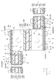
上記のように構成される本実施形態の回路基板1は、図3に示す回路基板製造中間体50の一部の絶縁層52が切除されることで第2実装部4が形成される。以下、図3を参照して回路基板製造中間体50の各構成について詳細に説明する。
In the circuit board 1 of the present embodiment configured as described above, the second mounting portion 4 is formed by removing a part of the insulating layer 52 of the circuit board manufacturing intermediate 50 shown in FIG. Hereinafter, each configuration of the circuit board manufacturing intermediate 50 will be described in detail with reference to FIG.
具体的には、回路基板製造中間体50は、回路基板1を製造する過程で作製される中間物である。回路基板製造中間体50は、実装面51と、絶縁層52と、導体層53と、剥離層54とを備え、絶縁層52の一部、及び、剥離層54を含む切除部位8が切除されることで第2実装部4が形成され、これにより、第1実装部3と第2実装部4とが一体となった上述の回路基板1が形成される(図2参照)。回路基板製造中間体50は、積層方向Xが板厚方向となる略矩形板状に形成され、ここでは、全体として上述の第1実装部3と第2実装部4とを合わせた形状に形成される。
Specifically, the circuit board manufacturing intermediate 50 is an intermediate manufactured in the process of manufacturing the circuit board 1. The circuit board manufacturing intermediate 50 includes a mounting surface 51, an insulating layer 52, a conductor layer 53, and a peeling layer 54, and a part of the insulating layer 52 and the cut site 8 including the peeling layer 54 are cut off. Thus, the second mounting portion 4 is formed, whereby the above-described circuit board 1 in which the first mounting portion 3 and the second mounting portion 4 are integrated is formed (see FIG. 2). The circuit board manufacturing intermediate 50 is formed in a substantially rectangular plate shape in which the stacking direction X is the plate thickness direction. Is done.
実装面51は、電子部品2が実装される面であり、上述した第1実装部3の実装面31、及び、第2実装部4の実装面41を構成する。回路基板製造中間体50は、積層方向Xの両面(両外面)がそれぞれ実装面51を構成する。実装面51は、切除部位8が切除された状態(図2参照)で、回路基板製造中間体50において、絶縁層52の延在方向、ここでは、短辺方向Yに互いに隣接する第1実装部形成領域3A、及び、第2実装部形成領域4Aのうちの第1実装部形成領域3Aに設けられた部分が上述の実装面31を構成し、第2実装部形成領域4Aに設けられた部分が上述の実装面41を構成する。ここで、第1実装部形成領域3Aは、回路基板製造中間体50において切除部位8が切除されることで第1実装部3を構成することとなる領域である。同様に、第2実装部形成領域4Aは、回路基板製造中間体50において切除部位8が切除されることで第2実装部4を構成することとなる領域である。ここでは、実装面51は、切除部位8が切除された状態で、回路基板製造中間体50の積層方向Xの一方側の面においては、一部が実装面31を構成し、残りの一部が実装面41を構成する。一方、実装面51は、切除部位8が切除された状態で、回路基板製造中間体50の積層方向Xの他方側の面においては、一部が実装面31を構成し、残りの一部が切除部位8として切除される部分となる。また、各実装面51は、実装面31を構成する第1実装部形成領域3Aには上述のソルダレジスト35が設けられ、実装面41を構成する第2実装部形成領域4Aには上述のソルダレジスト45が設けられる。なお、ソルダレジスト35、45は、実装面51において切除部位8として切除される部分には設けられていなくてもよいがここでは当該部分にまでソルダレジスト35が延在している。
The mounting surface 51 is a surface on which the electronic component 2 is mounted, and constitutes the mounting surface 31 of the first mounting unit 3 and the mounting surface 41 of the second mounting unit 4 described above. In the circuit board manufacturing intermediate 50, both surfaces (both outer surfaces) in the stacking direction X constitute the mounting surface 51. In the circuit board manufacturing intermediate 50, the mounting surface 51 is adjacent to each other in the extending direction of the insulating layer 52, in this case, the short side direction Y, in a state where the excision site 8 is excised (see FIG. 2). Of the part forming region 3A and the second mounting part forming region 4A, the portion provided in the first mounting part forming region 3A constitutes the mounting surface 31 described above, and is provided in the second mounting part forming region 4A. The portion constitutes the mounting surface 41 described above. Here, the first mounting portion forming region 3 </ b> A is a region that constitutes the first mounting portion 3 by cutting the cut portion 8 in the circuit board manufacturing intermediate 50. Similarly, the second mounting portion formation region 4 </ b> A is a region that constitutes the second mounting portion 4 by cutting the cut portion 8 in the circuit board manufacturing intermediate 50. Here, a part of the mounting surface 51 constitutes the mounting surface 31 on the one side surface in the stacking direction X of the circuit board manufacturing intermediate 50 in a state in which the excision site 8 is excised, and the remaining part. Constitutes the mounting surface 41. On the other hand, part of the mounting surface 51 constitutes the mounting surface 31 and the other part of the surface on the other side in the stacking direction X of the circuit board manufacturing intermediate 50 in a state where the excision site 8 is excised. It becomes a part to be excised as the excision site 8. In addition, each mounting surface 51 is provided with the above-described solder resist 35 in the first mounting portion forming region 3A constituting the mounting surface 31, and the above-described solder in the second mounting portion forming region 4A constituting the mounting surface 41. A resist 45 is provided. Note that the solder resists 35 and 45 may not be provided in a portion of the mounting surface 51 that is to be excised as the excision site 8, but here the solder resist 35 extends to the portion.
絶縁層52は、絶縁性の材料からなる層であり、切除部位8に相当する一部が切除された上で、上述した第1実装部3の絶縁層32、及び、第2実装部4の絶縁層42を構成する。絶縁層52は、複数が積層され、それぞれ積層方向Xが板厚方向となる略矩形状の平面層状に形成される。ここでは、回路基板製造中間体50は、絶縁層32と同様に、積層方向Xに沿って5層の絶縁層52が積層されている。回路基板製造中間体50における5つの絶縁層52は、第1実装部3と同様に、積層方向Xの一方側から他方側に向けて第1プリプレグ層52a、第2プリプレグ層52b、コア層52c、第3プリプレグ層52d、第4プリプレグ層52eの順で積層されている。そして、第1プリプレグ層52a、コア層52c、第3プリプレグ層52d、及び、第4プリプレグ層52eは、上述した連続絶縁層5と同様に、第1実装部3を構成することとなる第1実装部形成領域3Aと第2実装部4を構成することとなる第2実装部形成領域4Aとに渡って連続するように設けられる。一方、第2プリプレグ層52bは、第1実装部3を構成することとなる第1実装部形成領域3Aに設けられ、第2実装部4を構成することとなる第2実装部形成領域4Aまでは延在されない。
The insulating layer 52 is a layer made of an insulating material, and after the part corresponding to the excision site 8 is excised, the insulating layer 32 of the first mounting part 3 and the second mounting part 4 described above. An insulating layer 42 is formed. A plurality of insulating layers 52 are laminated, and each is formed in a substantially rectangular planar layer shape in which the laminating direction X is the plate thickness direction. Here, in the circuit board manufacturing intermediate 50, similarly to the insulating layer 32, five insulating layers 52 are stacked along the stacking direction X. The five insulating layers 52 in the circuit board manufacturing intermediate 50 are composed of the first prepreg layer 52a, the second prepreg layer 52b, and the core layer 52c from one side to the other side in the stacking direction X, as in the first mounting part 3. The third prepreg layer 52d and the fourth prepreg layer 52e are laminated in this order. The first prepreg layer 52a, the core layer 52c, the third prepreg layer 52d, and the fourth prepreg layer 52e constitute the first mounting portion 3 in the same manner as the continuous insulating layer 5 described above. The mounting portion forming region 3A and the second mounting portion forming region 4A that constitutes the second mounting portion 4 are provided so as to be continuous. On the other hand, the second prepreg layer 52b is provided in the first mounting portion forming region 3A that constitutes the first mounting portion 3, and reaches the second mounting portion forming region 4A that constitutes the second mounting portion 4. Is not extended.
ここでは、複数の絶縁層52のうち第1プリプレグ層52aは、切除部位8が切除された状態(図2参照)で、一部が第1プリプレグ層32aを構成し、残りの一部がプリプレグ層42aを構成する。つまり、第1プリプレグ層52aは、切除部位8が切除された状態で、上述した連続絶縁層5を構成する。複数の絶縁層52のうち第2プリプレグ層52bは、切除部位8が切除された状態で、第2プリプレグ層32bを構成する。つまり、第2プリプレグ層32bは、切除部位8が切除された状態で、上述した単独絶縁層7を構成する。複数の絶縁層52のうちコア層52cは、切除部位8が切除された状態で、一部がコア層32cを構成し、残りの一部が切除部位8をなす切除コア層92cを構成する。同様に、複数の絶縁層52のうち第3プリプレグ層52dは、切除部位8が切除された状態で、一部が第3プリプレグ層32dを構成し、残りの一部が切除部位8をなす第1切除プリプレグ層92dを構成する。また、複数の絶縁層52のうち第4プリプレグ層52eは、切除部位8が切除された状態で、一部が第4プリプレグ層32eを構成し、残りの一部が切除部位8をなす第2切除プリプレグ層92eを構成する。つまり、コア層52c、第3プリプレグ層52d、第4プリプレグ層52eは、それぞれ、切除部位8が切除された状態で、一部が単独絶縁層7を構成し、残りの一部が切除部位8として切除される切除絶縁層9を構成する。
Here, among the plurality of insulating layers 52, the first prepreg layer 52a is in a state in which the excision site 8 is excised (see FIG. 2), and a part of the first prepreg layer 52a constitutes the first prepreg layer 32a, and the remaining part of the prepreg layer 52a. Layer 42a is formed. That is, the 1st prepreg layer 52a comprises the continuous insulation layer 5 mentioned above in the state in which the excision site | part 8 was excised. Of the plurality of insulating layers 52, the second prepreg layer 52b constitutes the second prepreg layer 32b in a state where the excision site 8 is excised. That is, the second prepreg layer 32b forms the above-described single insulating layer 7 in a state where the excision site 8 is excised. Among the plurality of insulating layers 52, the core layer 52 c constitutes a core layer 32 c, part of which constitutes the core layer 32 c and the part of the core layer 52 c which forms the part of the excision 8 in a state where the excision part 8 is excised. Similarly, among the plurality of insulating layers 52, the third prepreg layer 52d is configured such that a part of the third prepreg layer 32d is formed in the state where the excision site 8 is excised, and the remaining part of the third prepreg layer 52d constitutes the excision site 8. One cut prepreg layer 92d is formed. Further, among the plurality of insulating layers 52, the fourth prepreg layer 52e is a state in which a part of the fourth prepreg layer 32e is formed in the state where the excision site 8 is excised, and the remaining part of the second prepreg layer 52e forms the excision site 8. The cut prepreg layer 92e is formed. That is, the core layer 52c, the third prepreg layer 52d, and the fourth prepreg layer 52e each constitute a single insulating layer 7 in a state where the excision site 8 is excised, and the remaining part of the core site 52c, the third prepreg layer 52d, and the fourth prepreg layer 52e. As shown in FIG.
導体層53は、導電性の材料からなり、少なくとも複数の絶縁層52の一部に設けられ電子部品2が電気的に接続される回路パターン34、44(後述する図9等参照)を形成するものであり、上述した第1実装部3の導体層33、及び、第2実装部4の導体層43を構成する。回路基板製造中間体50の導体層53は、外層回路体として、第1プリプレグ層52aの第2プリプレグ層52b側とは反対側の面、及び、第4プリプレグ層52eの第3プリプレグ層52d側とは反対側の面に設けられると共に、内層回路体として、第2プリプレグ層52bとコア層52cとの境界面、及び、コア層52cと第3プリプレグ層52dとの境界面に設けられ、これらが導体層33、導体層43を構成する。ここでは、第1プリプレグ層52aに設けられた導体層53は、一部が導体層33を構成し、残りの一部が導体層43を構成する。つまり、第1プリプレグ層52aの第2プリプレグ層52b側とは反対側の面に設けられた導体層53は、切除部位8が切除された状態で、上述した連続導体層6を構成する。連続導体層6以外の他の導体層53は、切除部位8が切除された状態で、一部が導体層33を構成し、残りの一部が切除部位8をなす切除導体層93を構成する。なお、導体層53は、切除部位8として切除される部分には設けられていなくてもよいがここでは当該部分にまで延在し、切除導体層93を構成するようにしている。
The conductor layer 53 is made of a conductive material, and is formed on at least a part of the plurality of insulating layers 52 to form circuit patterns 34 and 44 (see FIG. 9 to be described later) to which the electronic component 2 is electrically connected. The conductor layer 33 of the 1st mounting part 3 mentioned above and the conductor layer 43 of the 2nd mounting part 4 are comprised. The conductor layer 53 of the circuit board manufacturing intermediate 50 is, as an outer layer circuit body, a surface opposite to the second prepreg layer 52b side of the first prepreg layer 52a and the third prepreg layer 52d side of the fourth prepreg layer 52e. Are provided on the opposite surface, and are provided as inner layer circuit bodies on the boundary surface between the second prepreg layer 52b and the core layer 52c, and on the boundary surface between the core layer 52c and the third prepreg layer 52d. Constitutes the conductor layer 33 and the conductor layer 43. Here, a part of the conductor layer 53 provided in the first prepreg layer 52 a constitutes the conductor layer 33, and the remaining part constitutes the conductor layer 43. That is, the conductor layer 53 provided on the surface of the first prepreg layer 52a opposite to the second prepreg layer 52b side constitutes the above-described continuous conductor layer 6 in a state where the excision site 8 is excised. The conductor layer 53 other than the continuous conductor layer 6 constitutes the conductor layer 33 in a state where the excision site 8 is excised, and the remaining part constitutes the excision conductor layer 93 constituting the excision site 8. . The conductor layer 53 may not be provided in a portion to be excised as the excision site 8, but here extends to the portion to constitute the excision conductor layer 93.
剥離層54は、絶縁層52に対して剥離が容易な絶縁性の材料からなる層であり、第2実装部形成領域4Aに設けられ積層された複数の絶縁層52の間に介在し剥離界面54aを構成する。ここでは、剥離層54は、第2実装部形成領域4Aにおいて、積層された複数の絶縁層52のうち第1プリプレグ層52aとコア層52cとの間に介在し、第2プリプレグ層52bと隣接する位置に設けられる。剥離層54は、例えば、テトラフルオロエチレンの重合体でフッ素原子と炭素原子のみからなるフッ素樹脂(フッ化炭素樹脂、ポリテトラフルオロエチレン)等のテープによって形成される。剥離層54は、第2実装部形成領域4Aに連続絶縁層5(プリプレグ層42a)と接するようにして設けられ、当該連続絶縁層5との接触面が剥離界面54aを形成する。また、剥離層54と第2プリプレグ層52bとの接触面54bは、第1実装部形成領域3Aと第2実装部形成領域4Aとの境界面の一部を構成する。
The peeling layer 54 is a layer made of an insulating material that can be easily peeled from the insulating layer 52, and is interposed between the plurality of laminated insulating layers 52 provided in the second mounting portion formation region 4A. 54a is configured. Here, the release layer 54 is interposed between the first prepreg layer 52a and the core layer 52c among the plurality of stacked insulating layers 52 in the second mounting portion formation region 4A, and is adjacent to the second prepreg layer 52b. It is provided in the position to do. The release layer 54 is formed of, for example, a tape such as a fluororesin (fluorocarbon resin, polytetrafluoroethylene) that is a polymer of tetrafluoroethylene and includes only fluorine atoms and carbon atoms. The release layer 54 is provided in contact with the continuous insulating layer 5 (prepreg layer 42a) in the second mounting portion formation region 4A, and the contact surface with the continuous insulating layer 5 forms a release interface 54a. Further, the contact surface 54b between the release layer 54 and the second prepreg layer 52b constitutes a part of a boundary surface between the first mounting portion forming region 3A and the second mounting portion forming region 4A.
そして、上述の切除絶縁層9は、積層方向Xに対して当該剥離層54を挟んで連続絶縁層5とは反対側に位置し、上述した単独絶縁層7は、短辺方向Yに対して当該切除絶縁層9と当該剥離層54とに第1実装部形成領域3A側で隣接する。単独絶縁層7は、第2プリプレグ層32b、コア層52cの一部をなすコア層32c、第3プリプレグ層52dの一部をなす第3プリプレグ層32d、及び、第4プリプレグ層52eの一部をなす第4プリプレグ層32eを含んで構成される。また、切除絶縁層9は、コア層52cの残りの一部をなす切除コア層92c、第3プリプレグ層52dの残りの一部をなす第1切除プリプレグ層92d、及び、第4プリプレグ層52eの残りの一部をなす第2切除プリプレグ層92eを含んで構成される。ここでは、第1実装部3の複数の絶縁層32を構成する単独絶縁層7、及び、切除絶縁層9は、共に他の絶縁層(例えば、第1プリプレグ層52a、第2プリプレグ層52b、第3プリプレグ層52d、第4プリプレグ層52e等)より相対的に剛性が高いコア層32c、切除コア層92cを含む。そして、回路基板1を製造する過程で回路基板製造中間体50から切除される切除部位8は、上記切除絶縁層9、上記剥離層54、及び、上記切除導体層93によって構成される。
And the above-mentioned ablation insulating layer 9 is located on the opposite side to the continuous insulating layer 5 with the release layer 54 sandwiched in the stacking direction X, and the single insulating layer 7 described above is in the short side direction Y. The cut insulating layer 9 and the release layer 54 are adjacent to each other on the first mounting portion formation region 3A side. The single insulating layer 7 includes a second prepreg layer 32b, a core layer 32c that forms part of the core layer 52c, a third prepreg layer 32d that forms part of the third prepreg layer 52d, and a part of the fourth prepreg layer 52e. The fourth prepreg layer 32e is formed. The cut insulation layer 9 includes a cut core layer 92c that forms the remaining part of the core layer 52c, a first cut prepreg layer 92d that forms the remaining part of the third prepreg layer 52d, and a fourth prepreg layer 52e. The second excision prepreg layer 92e forming the remaining part is included. Here, the single insulating layer 7 and the cut insulating layer 9 constituting the plurality of insulating layers 32 of the first mounting portion 3 are both other insulating layers (for example, the first prepreg layer 52a, the second prepreg layer 52b, The third prepreg layer 52d, the fourth prepreg layer 52e, etc.) include a core layer 32c and a cut core layer 92c that are relatively rigid. The excision site 8 excised from the circuit board production intermediate 50 in the process of producing the circuit board 1 is constituted by the excision insulating layer 9, the release layer 54, and the excision conductor layer 93.
上記のように構成される回路基板製造中間体50は、切除部位8が切除されることで回路基板1が形成される際には、図4に示すように、第1実装部形成領域3Aと第2実装部形成領域4Aとの境界面、より詳細には、第2プリプレグ層52b(第2プリプレグ層32b)と剥離層54との接触面54bを含む領域に切削溝55が形成される。切削溝55は、連続導体層6側とは反対側、すなわち、第4プリプレグ層52e側から積層方向Xに沿って第4プリプレグ層52e、第3プリプレグ層52d、コア層52cを貫通し第2プリプレグ層52b、剥離層54のコア層52c側の面まで到達するように形成される。切削溝55は、長辺方向Zに対しては第1実装部形成領域3Aと第2実装部形成領域4Aとの境界面の全域に渡って延在して形成される。そして、回路基板製造中間体50は、切削溝55を境界として切除部位8を剥離層54の剥離界面54aから剥離し、図2に示すように、連続絶縁層5、単独絶縁層7等を残して当該切除部位8を切除することで、第1実装部形成領域3Aに第1実装部3を残したまま第2実装部形成領域4Aに第2実装部4が形成され、これにより、図1、図2に示すように、第1実装部3と第2実装部4とが一体となった上述の回路基板1が形成される。
When the circuit board 1 is formed by cutting away the excision site 8, the circuit board manufacturing intermediate 50 configured as described above has the first mounting portion forming region 3 </ b> A and the first mounting portion forming region 3 </ b> A as shown in FIG. 4. A cutting groove 55 is formed in the boundary surface with the second mounting portion formation region 4A, more specifically, in a region including the contact surface 54b between the second prepreg layer 52b (second prepreg layer 32b) and the release layer 54. The cutting groove 55 penetrates the fourth prepreg layer 52e, the third prepreg layer 52d, and the core layer 52c along the stacking direction X from the side opposite to the continuous conductor layer 6 side, that is, from the fourth prepreg layer 52e side. The prepreg layer 52b and the release layer 54 are formed so as to reach the surface on the core layer 52c side. The cutting groove 55 is formed so as to extend over the entire boundary surface between the first mounting portion forming region 3A and the second mounting portion forming region 4A in the long side direction Z. Then, the circuit board manufacturing intermediate 50 peels the excision site 8 from the peeling interface 54a of the peeling layer 54 with the cutting groove 55 as a boundary, leaving the continuous insulating layer 5, the single insulating layer 7 and the like as shown in FIG. By cutting away the excision site 8, the second mounting portion 4 is formed in the second mounting portion forming area 4A while leaving the first mounting portion 3 in the first mounting portion forming area 3A. As shown in FIG. 2, the above-described circuit board 1 in which the first mounting portion 3 and the second mounting portion 4 are integrated is formed.
この場合、回路基板1は、第1実装部3を構成する単独絶縁層7の第2実装部4側の端面7aの一部、ここでは、コア層32c、第3プリプレグ層32d、第4プリプレグ層32eの第2実装部4側の端面7aに切削溝55を形成する際に切削痕7b(図1参照)が形成される。つまり、第1実装部3は、第2実装部4側に位置する絶縁層32の端面7aが切削痕7bを有する。また、回路基板1は、第2実装部4において回路基板製造中間体50から切除された剥離層54の剥離界面54aと接触していたプリプレグ層42a(連続絶縁層5)側の界面が上述の絶縁層露出面4aとなり露出することとなる。なお、上記の切削溝55自体は、例えば、切除部位8の切除の直前に形成されてもよいし、回路基板製造中間体50への電子部品2の実装前に形成されてもよい。
In this case, the circuit board 1 is a part of the end surface 7a on the second mounting portion 4 side of the single insulating layer 7 constituting the first mounting portion 3, here, the core layer 32c, the third prepreg layer 32d, and the fourth prepreg. When the cutting groove 55 is formed in the end surface 7a on the second mounting portion 4 side of the layer 32e, a cutting mark 7b (see FIG. 1) is formed. That is, as for the 1st mounting part 3, the end surface 7a of the insulating layer 32 located in the 2nd mounting part 4 side has the cutting trace 7b. The circuit board 1 has an interface on the prepreg layer 42a (continuous insulating layer 5) side that is in contact with the peeling interface 54a of the peeling layer 54 cut out from the circuit board manufacturing intermediate 50 in the second mounting portion 4 described above. The insulating layer exposed surface 4a is exposed. In addition, said cutting groove 55 itself may be formed just before excision of excision site 8, for example, and may be formed before mounting electronic parts 2 to circuit board manufacture intermediate 50.
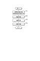
次に、図5、図6、図7を参照して上記のように構成される回路基板製造中間体50から回路基板1を製造する回路基板製造方法について説明する。なお、以下で説明する回路基板製造方法は、作業員が種々の装置、機器、治具等を用いて手作業で行うものとして説明するが、これに限らず、例えば、種々の製造装置によって自動で実行するものであってもよい。また、回路基板1、回路基板製造中間体50の各構成については、適宜上記で説明した図を参照する。
Next, a circuit board manufacturing method for manufacturing the circuit board 1 from the circuit board manufacturing intermediate 50 configured as described above will be described with reference to FIGS. 5, 6, and 7. In addition, although the circuit board manufacturing method described below is described as being performed manually by an operator using various devices, equipment, jigs, etc., the present invention is not limited to this, and for example, automatic operation by various manufacturing devices. May be executed. For the configurations of the circuit board 1 and the circuit board manufacturing intermediate 50, refer to the drawings described above as appropriate.
まず、作業員は、中間体作製工程として、回路基板1を製造する過程で作製される中間物である回路基板製造中間体50を作製する(ステップST1)。より詳細には、作業員は、各絶縁層52上に銅箔等の導体層53によって、要求される回路パターン34、44(後述する図9等参照)に応じたパターンを印刷し、エッチングによって不要な導体部分を除去することで回路パターン34、44を設ける。そして、作業員は、導体層53が設けられた複数の絶縁層52を、所定の位置(第2実装部形成領域4Aに相当する位置)に剥離層54を介在させながら層状に積層させ、当該各絶縁層52を相互に固着させ回路基板製造中間体50を形成する。また、作業員は、回路基板製造中間体50にソルダレジスト35、45やスルーホール21等も設ける。
First, an operator produces a circuit board manufacturing intermediate 50 that is an intermediate manufactured in the process of manufacturing the circuit board 1 as an intermediate manufacturing process (step ST1). More specifically, the worker prints a pattern corresponding to a required circuit pattern 34, 44 (see FIG. 9 described later) on each insulating layer 52 by a conductor layer 53 such as copper foil, and performs etching. Circuit patterns 34 and 44 are provided by removing unnecessary conductor portions. Then, the worker laminates the plurality of insulating layers 52 provided with the conductor layers 53 in a layered manner with the release layer 54 interposed at a predetermined position (a position corresponding to the second mounting portion formation region 4A). The insulating layers 52 are fixed to each other to form the circuit board manufacturing intermediate 50. The worker also provides solder resists 35 and 45, the through hole 21, and the like on the circuit board manufacturing intermediate 50.
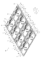
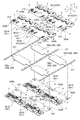
ここでは、回路基板製造中間体50は、図6に例示するように、複数が連結部としてのキャリア71によって連結され組基板化された中間体集合体70として作製される。つまり、本実施形態の中間体作製工程は、複数の回路基板製造中間体50がキャリア71によって組基板化された中間体集合体70を作製する中間体集合体作製工程でもある。中間体集合体70は、複数の回路基板製造中間体50が並んだ状態で、キャリア71によって当該複数の回路基板製造中間体50が相互に連結されて一体化されることで構成される。図6に例示する中間体集合体70は、短辺方向Yに沿って4つの回路基板製造中間体50が並び、長辺方向Zに沿ってそれぞれ2つの回路基板製造中間体50が並んで、合計8つの回路基板製造中間体50がキャリア71によって連結され一体化される。キャリア71は、各回路基板製造中間体50同士を連結するものであり、ここでは、短辺方向Yに棒状に延在して3つ、長辺方向Zに棒状に延在して4つが格子状に配置され、各キャリア71によって区画された空間部内に位置する各回路基板製造中間体50同士を連結する。中間体集合体70は、8つの回路基板製造中間体50が並んでキャリア71によって相互に連結された状態で、全体として長方形板状をなす。本実施形態の中間体集合体70は、短辺方向Yに沿って隣り合う回路基板製造中間体50において、第1実装部形成領域3Aと第2実装部形成領域4Aとが交互に位置するように、すなわち、短辺方向Yに隣り合う回路基板製造中間体50の一方の第1実装部形成領域3Aと他方の第2実装部形成領域4Aとが短辺方向Yに沿って隣り合うように配置される。
Here, as illustrated in FIG. 6, the circuit board manufacturing intermediate body 50 is manufactured as an intermediate body assembly 70 in which a plurality of circuit board manufacturing intermediate bodies 50 are connected by a carrier 71 as a connecting portion to form a board assembly. That is, the intermediate body manufacturing process of the present embodiment is also an intermediate body manufacturing process for manufacturing an intermediate body assembly 70 in which a plurality of circuit board manufacturing intermediate bodies 50 are assembled into a substrate by the carrier 71. The intermediate assembly 70 is configured by interconnecting and integrating the plurality of circuit board manufacturing intermediates 50 by a carrier 71 in a state where the plurality of circuit board manufacturing intermediates 50 are arranged. In the intermediate assembly 70 illustrated in FIG. 6, four circuit board manufacturing intermediates 50 are arranged along the short side direction Y, and two circuit board manufacturing intermediates 50 are arranged along the long side direction Z, respectively. A total of eight circuit board manufacturing intermediates 50 are connected and integrated by a carrier 71. The carrier 71 connects the circuit board manufacturing intermediates 50 to each other, and here, three are extended in a bar shape in the short side direction Y, and four are extended in a bar shape in the long side direction Z. The circuit board manufacturing intermediates 50 that are arranged in a shape and located in the space defined by the carriers 71 are connected to each other. The intermediate assembly 70 has a rectangular plate shape as a whole in a state where the eight circuit board manufacturing intermediate bodies 50 are arranged and connected to each other by the carrier 71. In the intermediate assembly 70 of the present embodiment, the first mounting portion formation regions 3A and the second mounting portion formation regions 4A are alternately positioned in the circuit board manufacturing intermediate 50 adjacent along the short side direction Y. In other words, one first mounting part forming region 3A and the other second mounting part forming region 4A of the circuit board manufacturing intermediate 50 adjacent to each other in the short side direction Y are adjacent to each other along the short side direction Y. Be placed.
この場合、作業員は、当該中間体作製工程(ステップST1)として、複数の回路基板製造中間体50が組基板化された中間体集合体70単位で上記のような導体層53の印刷、絶縁層52、剥離層54の積層、固着等の作業を行う。エッチングによる不要な導体部分の除去は、複数の回路基板製造中間体50が組基板化された中間体集合体70に対して施されてもよい。本実施形態の回路基板製造方法では、当該中間体作製工程(ステップST1)から切除工程(ステップST3)までの工程は、中間体集合体70に対して実施される。また、本実施形態では、作業員は、次の実装工程(ステップST2)の前に各回路基板製造中間体50に切削溝55を形成する。作業員は、各回路基板製造中間体50に対して第1実装部形成領域3Aと第2実装部形成領域4Aとの境界面、ここでは上述のように、第2プリプレグ層52b(第2プリプレグ層32b)と剥離層54との接触面54bを含む領域に切削溝55を形成する(図4参照)。
In this case, the worker prints and insulates the conductor layer 53 as described above in an intermediate assembly 70 unit in which a plurality of circuit board manufacturing intermediates 50 are assembled into a set substrate as the intermediate manufacturing step (step ST1). Operations such as laminating and fixing the layer 52 and the release layer 54 are performed. The removal of unnecessary conductor portions by etching may be performed on the intermediate assembly 70 in which the plurality of circuit board manufacturing intermediates 50 are formed into a combined substrate. In the circuit board manufacturing method of the present embodiment, the processes from the intermediate production process (step ST1) to the excision process (step ST3) are performed on the intermediate assembly 70. In the present embodiment, the worker forms the cutting groove 55 in each circuit board manufacturing intermediate 50 before the next mounting step (step ST2). The worker makes the second prepreg layer 52b (second prepreg layer 52b (second prepreg layer), as described above, to the boundary surface between the first mounting portion forming region 3A and the second mounting portion forming region 4A with respect to each circuit board manufacturing intermediate 50. A cutting groove 55 is formed in a region including the contact surface 54b between the layer 32b) and the release layer 54 (see FIG. 4).
次に、作業員は、実装工程として、回路基板製造中間体50の実装面51に電子部品2を実装する(ステップST2)。作業員は、実装工程では、回路基板製造中間体50の積層方向Xの両面の実装面51に、要求される電子部品2をそれぞれ実装する(図6等参照)。この場合、作業員は、当該実装工程(ステップST2)として、複数の回路基板製造中間体50が組基板化された中間体集合体70単位で上記のような電子部品2の実装等の作業を行う。
Next, the worker mounts the electronic component 2 on the mounting surface 51 of the circuit board manufacturing intermediate 50 as a mounting process (step ST2). In the mounting process, the worker mounts the required electronic components 2 on the mounting surfaces 51 on both sides in the stacking direction X of the circuit board manufacturing intermediate 50 (see FIG. 6 and the like). In this case, the worker performs, for example, the mounting of the electronic component 2 as described above in units of the intermediate assembly 70 in which the plurality of circuit board manufacturing intermediates 50 are assembled into a combined substrate as the mounting step (step ST2). Do.
次に、作業員は、切除工程として、回路基板製造中間体50の絶縁層52の一部を切除する(ステップST3)。より詳細には、作業員は、切除工程では、絶縁層52の一部を切除することで、絶縁層32が複数積層された第1実装部3と、絶縁層42の数が第1実装部3の絶縁層32の数より少ない第2実装部4とを形成し、少なくとも1つの絶縁層32、42、ここでは第1プリプレグ層32a、プリプレグ層42aを構成する第1プリプレグ層52aを、第1実装部3と第2実装部4とに渡って連続する連続絶縁層5とする。具体的には、作業員は、各回路基板製造中間体50において、事前に形成した切削溝55を境界として切除部位8を剥離層54の剥離界面54aで当該回路基板製造中間体50から剥離し、連続絶縁層5、単独絶縁層7等を残して当該切除部位8を切除することで、剥離層54と共に絶縁層52の一部として切除コア層92cを含む切除絶縁層9を切除する(図2参照)。これにより、作業員は、図7に示すように、第1実装部形成領域3Aに第1実装部3を残したまま第2実装部形成領域4Aに第2実装部4を形成し、第1実装部3と第2実装部4とが一体となった回路基板1を形成することができる。この場合、作業員は、当該切除工程(ステップST3)として、複数の回路基板製造中間体50が組基板化された中間体集合体70単位で上記のような切除部位8の切除等の作業を行う。なお、図7は、図6に示す中間体集合体70の積層方向Xの反対側の面を表している。
Next, the worker cuts off a part of the insulating layer 52 of the circuit board manufacturing intermediate 50 as a cutting process (step ST3). More specifically, in the cutting process, the worker cuts a part of the insulating layer 52 so that the first mounting part 3 in which a plurality of insulating layers 32 are stacked and the number of insulating layers 42 are the first mounting part. The second mounting portion 4 is formed in a number smaller than the number of the third insulating layers 32, and the first prepreg layer 52a constituting at least one insulating layer 32, 42, here the first prepreg layer 32a and the prepreg layer 42a, The continuous insulating layer 5 is continuous over the first mounting portion 3 and the second mounting portion 4. Specifically, in each circuit board manufacturing intermediate 50, the worker peels the excision site 8 from the circuit board manufacturing intermediate 50 at the peeling interface 54 a of the peeling layer 54 with the cutting groove 55 formed in advance as a boundary. Then, the ablation region 8 including the ablation core layer 92c as a part of the insulation layer 52 is excised together with the release layer 54 by excising the excision site 8 while leaving the continuous insulation layer 5, the single insulation layer 7 and the like (see FIG. 2). Thereby, as shown in FIG. 7, the worker forms the second mounting part 4 in the second mounting part forming area 4A while leaving the first mounting part 3 in the first mounting part forming area 3A. The circuit board 1 in which the mounting portion 3 and the second mounting portion 4 are integrated can be formed. In this case, the worker performs the above-described excision process (step ST3) such as excision of the excision site 8 in the unit of the aggregate assembly 70 in which the plurality of circuit board manufacturing intermediates 50 are assembled into a substrate. Do. FIG. 7 shows a surface on the opposite side of the stacking direction X of the intermediate assembly 70 shown in FIG.
次に、作業員は、切断工程として、各回路基板1とキャリア71との連結部分を切断し、各回路基板1を個片に切り分けて(ステップST4)、当該回路基板製造方法を終了する。
Next, as a cutting process, the worker cuts the connection portion between each circuit board 1 and the carrier 71, cuts each circuit board 1 into pieces (step ST4), and ends the circuit board manufacturing method.
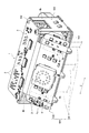
上記のように回路基板製造方法によって製造された回路基板1は、例えば、図8に示すような形状の電子部品ユニット100に適用される。図8に示す電子部品ユニット100は、自動車等の車両に搭載され、ワイヤハーネスWHに組み込まれる電子部品モジュールを構成するものである。ワイヤハーネスWHは、例えば、車両に搭載される各装置間の接続のために、電源供給や信号通信に用いられる複数の電線Wを束にして集合部品とし、コネクタ等で複数の電線Wを一度に各装置に接続するようにしたものである。ワイヤハーネスWHは、複数の電線Wと、当該電線Wと電気的に接続される電子部品ユニット100とを備える。電線Wは、例えば、複数の導電性の金属素線を撚り合わせた導体部(芯線)と、当該導体部の外側を覆う絶縁性の被覆部とを含んで構成される。ワイヤハーネスWHは、複数の電線Wを束ねて集約すると共に、束ねられた電線Wの端部に接続部としてのコネクタ等を介して電子部品ユニット100が電気的に接続される。ワイヤハーネスWHは、この他、さらに、グロメット、プロテクタ、固定具等を含んで構成されてもよい。電子部品ユニット100は、ワイヤハーネスWHにおいて車両に搭載されるバッテリ等の電源と、車両に搭載される各種の電子機器との間に接続され、電子部品2によって各種機能を実現する。
The circuit board 1 manufactured by the circuit board manufacturing method as described above is applied to, for example, an electronic component unit 100 having a shape as shown in FIG. The electronic component unit 100 shown in FIG. 8 is mounted on a vehicle such as an automobile and constitutes an electronic component module that is incorporated into the wire harness WH. The wire harness WH is, for example, a bundle of a plurality of electric wires W used for power supply and signal communication for connection between devices mounted on a vehicle to form a collective part. Are connected to each device. The wire harness WH includes a plurality of electric wires W and an electronic component unit 100 electrically connected to the electric wires W. The electric wire W includes, for example, a conductor portion (core wire) obtained by twisting a plurality of conductive metal strands and an insulating covering portion that covers the outside of the conductor portion. The wire harness WH bundles and aggregates a plurality of electric wires W, and the electronic component unit 100 is electrically connected to an end portion of the bundled electric wires W via a connector or the like as a connection portion. In addition to this, the wire harness WH may further include a grommet, a protector, a fixture, and the like. The electronic component unit 100 is connected between a power source such as a battery mounted on the vehicle in the wire harness WH and various electronic devices mounted on the vehicle, and realizes various functions by the electronic component 2.
電子部品ユニット100は、筐体101に回路基板1が組み付けられる。筐体101は、絶縁性の合成樹脂によって形成される。筐体101は、複数の部品が組み合わせられて構成されてもよいし、全体が一体で形成されてもよい。ここでは、回路基板1は、第1実装部3に対して第2実装部4が屈曲した位置関係となる状態で筐体101にボルト等の締結部材を介して組み付けられる。言い換えれば、回路基板1は、筐体101に組み付けられた状態で第1実装部3を含む仮想平面と第2実装部4を含む仮想平面とが交差する。ここでは、回路基板1は、相対的に剛性が高いリジッド部を構成する第1実装部3が筐体101における第1組み付け面102に固定され、相対的に可撓性が高いフレキシブル部を構成する第2実装部4が第2組み付け面103に固定される。第1組み付け面102と第2組み付け面103とは、互いに隣り合う異なる面であり、互いに交差する方向に延在する。回路基板1は、第1組み付け面102に固定され相対的に屈曲し難い第1実装部3に対して相対的に屈曲しやすい第2実装部4が屈曲した状態で第2組み付け面103に固定される。
In the electronic component unit 100, the circuit board 1 is assembled to the housing 101. The casing 101 is made of an insulating synthetic resin. The housing 101 may be configured by combining a plurality of components, or may be integrally formed as a whole. Here, the circuit board 1 is assembled to the housing 101 via a fastening member such as a bolt in a state in which the second mounting portion 4 is bent with respect to the first mounting portion 3. In other words, in the circuit board 1, the virtual plane including the first mounting unit 3 and the virtual plane including the second mounting unit 4 intersect with each other in the state of being assembled to the housing 101. Here, the circuit board 1 is configured such that a first mounting portion 3 constituting a rigid portion having relatively high rigidity is fixed to the first assembly surface 102 in the housing 101, thereby forming a flexible portion having relatively high flexibility. The second mounting portion 4 is fixed to the second assembly surface 103. The first assembly surface 102 and the second assembly surface 103 are different surfaces adjacent to each other, and extend in directions intersecting with each other. The circuit board 1 is fixed to the second assembly surface 103 in a state in which the second mounting portion 4 that is fixed relative to the first mounting portion 3 that is fixed to the first mounting surface 102 and is relatively difficult to bend is bent. Is done.
また、本実施形態の電子部品ユニット100は、第2組み付け面103自体が屈曲を有しており、ここでは、第2組み付け面103は、3次曲面として形成される。この場合、回路基板1は、3次曲面として形成される第2組み付け面103に対して相対的に可撓性が高い第2実装部4がさらに当該第2組み付け面103の形状に合わせて湾曲し追従して固定される。ここでは、第2実装部4は、長辺方向Zの両端側において、切り欠き部4bが形成された部分から第2組み付け面103の形状に合わせて3次曲面に湾曲し、湾曲した状態で第2組み付け面103に固定される。
Further, in the electronic component unit 100 of the present embodiment, the second assembly surface 103 itself has a bend, and here, the second assembly surface 103 is formed as a tertiary curved surface. In this case, the circuit board 1 has a second mounting portion 4 that is relatively flexible with respect to the second assembly surface 103 formed as a cubic curved surface, and is further curved to match the shape of the second assembly surface 103. Then follow and fix. Here, the second mounting portion 4 is curved to a tertiary curved surface in accordance with the shape of the second assembly surface 103 from the portion where the notch portion 4b is formed on both ends in the long side direction Z, and in a curved state. It is fixed to the second assembly surface 103.
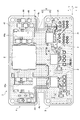
また、本実施形態の回路基板1は、上記のように第2組み付け面103の形状に第2実装部4をより好適に追従させることができるように、図9に示すように、当該第2実装部4に屈曲容易部46が設けられる。当該図9は、回路基板1の連続絶縁層5(図2参照)側の実装面31、41の導体層33、43(連続導体層6)による回路パターン34、44を表している。屈曲容易部46は、第2実装部4の導体層43(連続導体層6)が形成する回路パターン44の余白部分44aにより他の部位より可撓性が高い部分として形成される。第2実装部4において、導体層43が形成されていない余白部分44aは、導体層43が形成されている回路パターン44の部分と比較して相対的に可撓性が高い部分として形成される。第2実装部4は、第2組み付け面103の形状に応じて屈曲する部分に当該余白部分44aが設けられることで、当該屈曲容易部46が形成される。ここでは、屈曲容易部46は、第2実装部4において第2組み付け面103の形状に応じて屈曲する部分の稜線4c(図8参照)の近傍に当該稜線4cに沿ってそれぞれ形成される。図9の例では、屈曲容易部46は、第2実装部4において、各切り欠き部4bの近傍から、屈曲した際に形成される稜線4cの方向、ここでは短辺方向Yに沿って延在する。この場合、上述した回路基板製造方法における中間体作製工程(ステップST1)は、当該屈曲容易部46を形成する屈曲容易部形成工程を含む(図5参照)。すなわち、作業員は、中間体作製工程(ステップST1)では、屈曲容易部形成工程として、各絶縁層52上に銅箔等の導体層53によって、要求される回路パターン44を設ける際に、各屈曲容易部46に相当する相当する部分がくり抜かれるようにして当該回路パターン44を印刷し各余白部分44aを各屈曲容易部46として形成する作業もあわせて行う。
Further, the circuit board 1 of the present embodiment has the second mounting portion 4 as shown in FIG. 9 so that the second mounting portion 4 can follow the shape of the second assembly surface 103 more preferably as described above. A bendable portion 46 is provided on the mounting portion 4. FIG. 9 shows circuit patterns 34 and 44 by the conductor layers 33 and 43 (continuous conductor layer 6) of the mounting surfaces 31 and 41 on the continuous insulating layer 5 (see FIG. 2) side of the circuit board 1. The easy-to-bend portion 46 is formed as a portion having higher flexibility than other portions by the blank portion 44a of the circuit pattern 44 formed by the conductor layer 43 (continuous conductor layer 6) of the second mounting portion 4. In the second mounting portion 4, the blank portion 44 a where the conductor layer 43 is not formed is formed as a portion that is relatively more flexible than the portion of the circuit pattern 44 where the conductor layer 43 is formed. . The second mounting portion 4 is provided with the blank portion 44 a in a portion that bends according to the shape of the second assembly surface 103, whereby the bendable portion 46 is formed. Here, the bendable portion 46 is formed along the ridgeline 4c in the vicinity of the ridgeline 4c (see FIG. 8) of the portion that is bent according to the shape of the second assembly surface 103 in the second mounting portion 4. In the example of FIG. 9, the easy-to-bend portion 46 extends from the vicinity of each notch portion 4 b in the second mounting portion 4 along the direction of the ridge line 4 c formed when bent, in this case, the short side direction Y. Exists. In this case, the intermediate production step (step ST1) in the circuit board manufacturing method described above includes an easy-bend portion forming step for forming the easy-bend portion 46 (see FIG. 5). In other words, in the intermediate manufacturing process (step ST1), the worker provides each circuit layer 44 required by the conductor layer 53 such as copper foil on each insulating layer 52 as the easy-bending portion forming process. The circuit pattern 44 is printed so that a corresponding portion corresponding to the easily bendable portion 46 is cut out, and each marginal portion 44 a is formed as each easily bendable portion 46.
以上で説明した回路基板1によれば、電子部品2が実装される実装面31、41、絶縁性の絶縁層32、42、及び、絶縁層32、42に設けられ電子部品2が電気的に接続される導電性の導体層33、43をそれぞれ有する第1実装部3、及び、第2実装部4を備え、第1実装部3は、絶縁層32が複数積層され、第2実装部4は、絶縁層42の数が第1実装部3の絶縁層32の数より少なく、少なくとも1つの絶縁層32、42は、第1実装部3と第2実装部4とに渡って連続する連続絶縁層5である。
According to the circuit board 1 described above, the mounting surfaces 31 and 41 on which the electronic component 2 is mounted, the insulating insulating layers 32 and 42, and the electronic component 2 provided on the insulating layers 32 and 42 are electrically connected. The first mounting portion 3 and the second mounting portion 4 each having conductive conductor layers 33 and 43 to be connected are provided. The first mounting portion 3 includes a plurality of insulating layers 32 stacked, and the second mounting portion 4. The number of the insulating layers 42 is smaller than the number of the insulating layers 32 of the first mounting portion 3, and at least one insulating layer 32, 42 is continuous across the first mounting portion 3 and the second mounting portion 4. Insulating layer 5.
以上で説明した回路基板製造方法によれば、電子部品2が実装される実装面51、積層された複数の絶縁性の絶縁層52、及び、少なくとも複数の絶縁層52の一部に設けられ電子部品2が電気的に接続される導電性の導体層53を備える回路基板製造中間体50の実装面51に電子部品2を実装する実装工程(ステップST2)と、実装工程(ステップST2)の後に、回路基板製造中間体50の絶縁層52の一部を切除する切除工程(ステップST3)とを含む。つまり、以上で説明した回路基板製造方法によれば、切除工程(ステップST3)では、絶縁層52の一部を切除することで、絶縁層32が複数積層された第1実装部3と、絶縁層42の数が第1実装部3の絶縁層32の数より少ない第2実装部4とを形成し、少なくとも1つの絶縁層52を、第1実装部3と第2実装部4とに渡って連続する連続絶縁層5とする。
According to the circuit board manufacturing method described above, the mounting surface 51 on which the electronic component 2 is mounted, the plurality of stacked insulating insulating layers 52, and at least part of the plurality of insulating layers 52 are provided with the electronic components. After the mounting process (step ST2) for mounting the electronic component 2 on the mounting surface 51 of the circuit board manufacturing intermediate 50 including the conductive conductor layer 53 to which the component 2 is electrically connected, and after the mounting process (step ST2) And a cutting step (step ST3) of cutting a part of the insulating layer 52 of the circuit board manufacturing intermediate 50. That is, according to the circuit board manufacturing method described above, in the cutting process (step ST3), the insulating layer 52 is partly cut so that the first mounting portion 3 in which a plurality of insulating layers 32 are stacked and the insulating layer 52 are insulated. The second mounting part 4 is formed so that the number of the layers 42 is smaller than the number of the insulating layers 32 of the first mounting part 3, and at least one insulating layer 52 is extended over the first mounting part 3 and the second mounting part 4. The continuous insulating layer 5 is continuous.
以上で説明した回路基板製造中間体50によれば、電子部品2が実装される実装面51と、積層された複数の絶縁性の絶縁層52と、少なくとも複数の絶縁層52の一部に設けられ電子部品2が電気的に接続される導電性の導体層53と、絶縁層52の延在方向に互いに隣接する第1実装部形成領域3A、及び、第2実装部形成領域4Aのうちの第2実装部形成領域4Aに設けられ積層された複数の絶縁層52の間に介在し剥離界面54aを構成する剥離層54とを備え、複数の絶縁層52は、第1実装部形成領域3Aと第2実装部形成領域4Aとに渡って連続する連続絶縁層5、当該複数の絶縁層52の積層方向Xに対して剥離層54を挟んで連続絶縁層5とは反対側に位置する切除絶縁層9、及び、延在方向、ここでは、短辺方向Yに対して切除絶縁層9と剥離層54とに第1実装部形成領域3A側で隣接する単独絶縁層7を含んで構成される。
According to the circuit board manufacturing intermediate 50 described above, the mounting surface 51 on which the electronic component 2 is mounted, a plurality of laminated insulating layers 52, and at least a part of the plurality of insulating layers 52 are provided. Of the conductive mounting layer 53 to which the electronic component 2 is electrically connected, the first mounting portion forming region 3A, and the second mounting portion forming region 4A adjacent to each other in the extending direction of the insulating layer 52. A plurality of insulating layers 52 provided in the second mounting portion forming region 4A and interposed between the plurality of stacked insulating layers 52 to form a peeling interface 54a. The plurality of insulating layers 52 are formed in the first mounting portion forming region 3A. And a continuous insulating layer 5 continuous over the second mounting portion forming region 4A, and an ablation located on the opposite side of the continuous insulating layer 5 with the release layer 54 interposed in the stacking direction X of the plurality of insulating layers 52 Insulating layer 9 and the extending direction, here the short side direction Y Configured to include a single insulating layer 7 adjacent the first mounting portion forming area 3A side resection insulating layer 9 and the release layer 54 Te.
この場合、以上で説明した回路基板製造方法によれば、実装工程(ステップST2)の前に、絶縁層52の延在方向、ここでは、短辺方向Yに互いに隣接する第1実装部形成領域3A、及び、第2実装部形成領域4Aのうちの第2実装部形成領域4Aに設けられ積層された複数の絶縁層52の間に介在し剥離界面54aを構成する剥離層54を備え、複数の絶縁層52が、第1実装部形成領域3Aと第2実装部形成領域4Aとに渡って連続する連続絶縁層5、当該複数の絶縁層52の積層方向Xに対して剥離層54を挟んで連続絶縁層5とは反対側に位置する切除絶縁層9、及び、短辺方向Yに対して切除絶縁層9と剥離層54とに第1実装部形成領域3A側で隣接する単独絶縁層7を含んで構成される回路基板製造中間体50を作製する中間体作製工程(ステップST1)を含み、切除工程(ステップST3)では、剥離層54と共に切除絶縁層9を切除する。
In this case, according to the circuit board manufacturing method described above, the first mounting portion forming regions adjacent to each other in the extending direction of the insulating layer 52, here, the short side direction Y, before the mounting step (step ST2). 3A and a plurality of release layers 54 that are provided in the second mounting portion formation region 4A of the second mounting portion formation regions 4A and are interposed between the plurality of laminated insulating layers 52 to form a release interface 54a. The insulating layer 52 has a continuous insulating layer 5 continuous over the first mounting portion forming region 3A and the second mounting portion forming region 4A, and sandwiches the release layer 54 with respect to the stacking direction X of the plurality of insulating layers 52. The ablation insulating layer 9 located on the opposite side of the continuous insulation layer 5 and the single insulation layer adjacent to the ablation insulation layer 9 and the release layer 54 in the short side direction Y on the first mounting portion formation region 3A side. Manufacturing a circuit board manufacturing intermediate 50 comprising 7 Includes a body preparing step (step ST1), the ablation process (step ST3), to ablate the ablation insulating layer 9 with a release layer 54.
したがって、回路基板1、回路基板製造方法、及び、回路基板製造中間体50では、第2実装部4の絶縁層42の数が第1実装部3の絶縁層32の数より少なくされることで、第1実装部3を相対的に剛性が高いリジッド部とする一方、第2実装部4を相対的に可撓性が高いフレキシブル部とすることができると共に、連続絶縁層5が第1実装部3と第2実装部4とに渡って連続することで、これら相対的に剛性が高い第1実装部3と相対的に可撓性が高い第2実装部4とを一体とした当該回路基板1を製造することができる。ここでは、回路基板1は、第1実装部3と第2実装部4とが連続導体層6を介して電気的に接続されている。
Therefore, in the circuit board 1, the circuit board manufacturing method, and the circuit board manufacturing intermediate 50, the number of the insulating layers 42 of the second mounting part 4 is made smaller than the number of the insulating layers 32 of the first mounting part 3. While the first mounting portion 3 can be a rigid portion having relatively high rigidity, the second mounting portion 4 can be a flexible portion having relatively high flexibility, and the continuous insulating layer 5 can be used for the first mounting. The circuit in which the first mounting portion 3 having relatively high rigidity and the second mounting portion 4 having relatively high flexibility are integrated with each other by continuing over the portion 3 and the second mounting portion 4. The substrate 1 can be manufactured. Here, in the circuit board 1, the first mounting portion 3 and the second mounting portion 4 are electrically connected via the continuous conductor layer 6.
この場合、回路基板1、回路基板製造方法、及び、回路基板製造中間体50では、回路基板製造中間体50の実装面51に電子部品2を実装した後に絶縁層52の一部、ここでは、切除絶縁層9を切除することで、実装面31、41に電子部品2が実装された状態の第1実装部3、第2実装部4を形成することができ、相対的に剛性が高い第1実装部3と相対的に可撓性が高い第2実装部4とを一体とした回路基板1を製造することができる。このとき、回路基板1、回路基板製造方法、及び、回路基板製造中間体50では、回路基板製造中間体50の絶縁層52において、切除絶縁層9として切除されずに残った絶縁層52の一部が第1実装部3と第2実装部4とに渡って連続する連続絶縁層5を構成し、他の一部が第2実装部4を構成せず第1実装部3単体における単独絶縁層7を構成する。
In this case, in the circuit board 1, the circuit board manufacturing method, and the circuit board manufacturing intermediate 50, after mounting the electronic component 2 on the mounting surface 51 of the circuit board manufacturing intermediate 50, a part of the insulating layer 52, here, By cutting away the cut insulating layer 9, the first mounting portion 3 and the second mounting portion 4 in a state in which the electronic component 2 is mounted on the mounting surfaces 31, 41 can be formed, and the first portion having relatively high rigidity can be formed. The circuit board 1 in which the first mounting portion 3 and the relatively flexible second mounting portion 4 are integrated can be manufactured. At this time, in the circuit board 1, the circuit board manufacturing method, and the circuit board manufacturing intermediate 50, the insulating layer 52 of the circuit board manufacturing intermediate 50 is a part of the insulating layer 52 that remains without being cut as the cut insulating layer 9. The part constitutes a continuous insulating layer 5 continuous over the first mounting part 3 and the second mounting part 4, and the other part does not constitute the second mounting part 4, and the first mounting part 3 alone is isolated. Layer 7 is formed.
つまり、回路基板1、回路基板製造方法、及び、回路基板製造中間体50では、回路基板製造中間体50において第2実装部4を構成することとなる第2実装部形成領域4Aが第1実装部3を構成することとなる第1実装部形成領域3Aと同様に相対的に高い剛性を確保できている状態で、実装面41に電子部品2を実装することができる。これにより、回路基板1、回路基板製造方法、及び、回路基板製造中間体50では、例えば、可撓性が高い第2実装部4に対して特有の実装工程を設けなくても、一般的に用いられる電子部品実装用の設備を利用して実装面31及び実装面41に対してまとめて電子部品2を実装することができるので、製造コストの増加を抑制することができる。また、回路基板1、回路基板製造方法、及び、回路基板製造中間体50では、上記のように複数の回路基板製造中間体50を組基板化して中間体集合体70を構成した上で、当該中間体集合体70に対してまとめて電子部品2の実装を行うことができ、製造効率を向上することができるので、この点でも製造コストの増加を抑制することができる。
That is, in the circuit board 1, the circuit board manufacturing method, and the circuit board manufacturing intermediate 50, the second mounting portion formation region 4 </ b> A that constitutes the second mounting portion 4 in the circuit board manufacturing intermediate 50 is the first mounting. The electronic component 2 can be mounted on the mounting surface 41 in a state where relatively high rigidity can be ensured similarly to the first mounting portion formation region 3A that constitutes the portion 3. Thereby, in the circuit board 1, the circuit board manufacturing method, and the circuit board manufacturing intermediate 50, for example, even if a specific mounting process is not provided for the highly flexible second mounting portion 4, for example, Since the electronic component 2 can be mounted collectively on the mounting surface 31 and the mounting surface 41 using the electronic component mounting equipment used, an increase in manufacturing cost can be suppressed. Further, in the circuit board 1, the circuit board manufacturing method, and the circuit board manufacturing intermediate 50, the plurality of circuit board manufacturing intermediates 50 are assembled into a substrate as described above, and the intermediate assembly 70 is configured. Since the electronic component 2 can be mounted together on the intermediate assembly 70 and manufacturing efficiency can be improved, an increase in manufacturing cost can also be suppressed in this respect.
その上で、回路基板1、回路基板製造方法、及び、回路基板製造中間体50では、絶縁層52の一部、ここでは、切除絶縁層9を切除することで、上記のように相対的に剛性が高い第1実装部3と相対的に可撓性が高い第2実装部4とを一体とした回路基板1を製造することができる。そして、回路基板1、回路基板製造方法、及び、回路基板製造中間体50では、相対的に剛性が高い第1実装部3だけでなく相対的に可撓性が高い第2実装部4にも電子部品2を実装した上で、当該電子部品2が実装されている第2実装部4自体を種々の形状に追従することができる。
In addition, in the circuit board 1, the circuit board manufacturing method, and the circuit board manufacturing intermediate 50, a part of the insulating layer 52, here, the cut insulating layer 9 is cut away, so that The circuit board 1 in which the first mounting part 3 having high rigidity and the second mounting part 4 having relatively high flexibility are integrated can be manufactured. And in the circuit board 1, the circuit board manufacturing method, and the circuit board manufacturing intermediate 50, not only the relatively rigid first mounting part 3 but also the relatively flexible second mounting part 4 is used. After mounting the electronic component 2, the second mounting portion 4 itself on which the electronic component 2 is mounted can follow various shapes.
この結果、回路基板1、回路基板製造方法、及び、回路基板製造中間体50では、電子部品2が実装されている部分も含め、適正に種々の形状に追従することができる。また、回路基板1、回路基板製造方法、及び、回路基板製造中間体50では、第2実装部4が相対的に薄く構成され高い可撓性を有する構成であるので、当該第2実装部4において回路基板1と電子部品2との膨張係数の相違による影響を吸収することができ、これにより、熱伸縮等に対しても追従しやすい構成とすることができる。これにより、回路基板1、回路基板製造方法、及び、回路基板製造中間体50では、例えば、実装面41に実装される電子部品2とのハンダ接合部にかかる熱応力を抑制し当該ハンダ接合部等を適正に保護することができ、例えば、熱衝撃試験(Thermal Shock Test)においてもより良好な結果を得ることができる。また、回路基板1、回路基板製造方法、及び、回路基板製造中間体50では、第1実装部3と第2実装部4とを一体とした回路基板1とすることができるので、第1実装部3と第2実装部4とを接続するためのコネクタ等の構成やこれらを組み付ける工程を抑制することができ、この点でも製造コストの増加を抑制することができる。
As a result, in the circuit board 1, the circuit board manufacturing method, and the circuit board manufacturing intermediate 50, it is possible to appropriately follow various shapes including the portion where the electronic component 2 is mounted. In the circuit board 1, the circuit board manufacturing method, and the circuit board manufacturing intermediate 50, the second mounting portion 4 is configured to be relatively thin and highly flexible. Therefore, it is possible to absorb the influence due to the difference in expansion coefficient between the circuit board 1 and the electronic component 2, thereby making it possible to easily follow thermal expansion and contraction. Thereby, in the circuit board 1, the circuit board manufacturing method, and the circuit board manufacturing intermediate 50, for example, the thermal stress applied to the solder joint portion with the electronic component 2 mounted on the mounting surface 41 is suppressed, and the solder joint portion. Etc. can be properly protected, and for example, better results can be obtained even in a thermal shock test. In the circuit board 1, the circuit board manufacturing method, and the circuit board manufacturing intermediate 50, the first mounting portion 3 and the second mounting portion 4 can be integrated into the circuit board 1. The structure of a connector or the like for connecting the part 3 and the second mounting part 4 and the process of assembling them can be suppressed, and an increase in manufacturing cost can also be suppressed in this respect.
また、以上で説明した回路基板1、回路基板製造方法、及び、回路基板製造中間体50によれば、第1実装部3は、連続絶縁層5以外の絶縁層32、すなわち、単独絶縁層7の端面7aが第2実装部4側に位置し、さらに言えば、当該第2実装部4側に位置する絶縁層32(単独絶縁層7)の端面7aが切削痕7bを有する場合がある。つまり、回路基板1、回路基板製造方法、及び、回路基板製造中間体50によれば、回路基板製造中間体50の絶縁層52の一部、ここでは、切除絶縁層9を切除し第1実装部3、第2実装部4を形成することで、第1実装部3の単独絶縁層7の端面7aが第2実装部4側に位置することとなり、切除絶縁層9を切除する際に生じる切削痕7bが当該端面7aに形成される場合がある。
In addition, according to the circuit board 1, the circuit board manufacturing method, and the circuit board manufacturing intermediate 50 described above, the first mounting portion 3 has the insulating layer 32 other than the continuous insulating layer 5, that is, the single insulating layer 7. In other words, the end surface 7a of the insulating layer 32 (single insulating layer 7) positioned on the second mounting portion 4 side may have a cutting mark 7b. That is, according to the circuit board 1, the circuit board manufacturing method, and the circuit board manufacturing intermediate 50, a part of the insulating layer 52 of the circuit board manufacturing intermediate 50, here, the cut insulating layer 9 is cut out and the first mounting is performed. By forming the portion 3 and the second mounting portion 4, the end surface 7 a of the single insulating layer 7 of the first mounting portion 3 is positioned on the second mounting portion 4 side, which occurs when the cut insulating layer 9 is cut off. A cutting mark 7b may be formed on the end surface 7a.
また、以上で説明した回路基板1、回路基板製造方法、及び、回路基板製造中間体50によれば、第1実装部3の複数の絶縁層32は、他の絶縁層32、例えば、第1プリプレグ層32a、第2プリプレグ層32b、第3プリプレグ層32d、第4プリプレグ層32e等より相対的に剛性が高く端面7aが第2実装部4側に位置するコア層32cを含む。言い換えれば、以上で説明した回路基板1、回路基板製造方法、及び、回路基板製造中間体50によれば、単独絶縁層7、及び、切除絶縁層9は、他の絶縁層32、例えば、第1プリプレグ層32a、第2プリプレグ層32b、第3プリプレグ層32d、第4プリプレグ層32e等より相対的に剛性が高いコア層32c、切除コア層92cを含む。この場合、以上で説明した回路基板1、回路基板製造方法、及び、回路基板製造中間体50によれば、切除工程(ステップST3)では、相対的に剛性が高い切除コア層92cを含む切除絶縁層9を切除する。したがって、回路基板1、回路基板製造方法、及び、回路基板製造中間体50では、第2実装部4の絶縁層42においてコア層32c、切除コア層92cのように相対的に剛性が高い層を含まない構成とすることができるので、第2実装部4を第1実装部3と比較して十分に可撓性が高い部分とすることができ、より適正に種々の形状に追従することができる。
In addition, according to the circuit board 1, the circuit board manufacturing method, and the circuit board manufacturing intermediate 50 described above, the plurality of insulating layers 32 of the first mounting unit 3 are the other insulating layers 32, for example, the first The prepreg layer 32a, the second prepreg layer 32b, the third prepreg layer 32d, the fourth prepreg layer 32e, etc. include a core layer 32c that is relatively rigid and has an end surface 7a located on the second mounting portion 4 side. In other words, according to the circuit board 1, the circuit board manufacturing method, and the circuit board manufacturing intermediate 50 described above, the single insulating layer 7 and the cut insulating layer 9 are the other insulating layers 32, for example, the first It includes a core layer 32c and an ablation core layer 92c having relatively higher rigidity than the first prepreg layer 32a, the second prepreg layer 32b, the third prepreg layer 32d, the fourth prepreg layer 32e, and the like. In this case, according to the circuit board 1, the circuit board manufacturing method, and the circuit board manufacturing intermediate 50 described above, in the cutting process (step ST3), the cutting insulation including the cutting core layer 92c having relatively high rigidity. Layer 9 is excised. Therefore, in the circuit board 1, the circuit board manufacturing method, and the circuit board manufacturing intermediate 50, the insulating layer 42 of the second mounting portion 4 is provided with a layer having relatively high rigidity such as the core layer 32c and the cut core layer 92c. Since it can be configured not to include, the second mounting portion 4 can be a sufficiently flexible portion compared to the first mounting portion 3, and can follow various shapes more appropriately. it can.
さらに、以上で説明した回路基板1、回路基板製造方法、及び、回路基板製造中間体50によれば、第2実装部4は、導体層43が形成する回路パターン44の余白部分44aにより他の部位より可撓性が高く形成される屈曲容易部46を有する。この場合、以上で説明した回路基板1、回路基板製造方法、及び、回路基板製造中間体50によれば、中間体作製工程(ステップST1)において、導体層53が形成する回路パターン44の余白部分44aにより他の部位より可撓性が高く形成される屈曲容易部46を形成する屈曲容易部形成工程を含む。したがって、回路基板1、回路基板製造方法、及び、回路基板製造中間体50では、相対的に高い可撓性を有し高い形状追従性能を有する第2実装部4において、より可撓性が高く形成される屈曲容易部46を基点として変形しやすくすることができるので、第2実装部4が設けられる部分の形状に合わせて屈曲することでより好適に種々の形状に追従させることができる。言い換えれば、回路基板1、回路基板製造方法、及び、回路基板製造中間体50では、回路パターン44の余白部分44aとして形成される屈曲容易部46の周りの導体層53の縁部が曲げガイド部となることで当該屈曲容易部46を基点として変形しやすくしより良好な形状追従性を確保することができる。また、回路基板1、回路基板製造方法、及び、回路基板製造中間体50では、第2実装部4が当該屈曲容易部46を基点として変形することで、当該第2実装部4に実装されている電子部品2の向きを任意に微調整することができ、例えば、電子部品2を構成するLED素子、スピーカ等の向きを好みの向きに微調整することができる構成を採用することができる。
Furthermore, according to the circuit board 1, the circuit board manufacturing method, and the circuit board manufacturing intermediate 50 described above, the second mounting portion 4 is replaced with another one by the blank portion 44 a of the circuit pattern 44 formed by the conductor layer 43. It has an easy-to-bend portion 46 that is more flexible than the portion. In this case, according to the circuit board 1, the circuit board manufacturing method, and the circuit board manufacturing intermediate 50 described above, the blank portion of the circuit pattern 44 formed by the conductor layer 53 in the intermediate manufacturing step (step ST1). 44b includes an easily bendable portion forming step of forming an easily bendable portion 46 that is formed with higher flexibility than other portions by 44a. Therefore, in the circuit board 1, the circuit board manufacturing method, and the circuit board manufacturing intermediate 50, the second mounting portion 4 having relatively high flexibility and high shape following performance has higher flexibility. Since the easily bent portion 46 to be formed can be easily deformed, it is possible to follow various shapes more suitably by bending according to the shape of the portion where the second mounting portion 4 is provided. In other words, in the circuit board 1, the circuit board manufacturing method, and the circuit board manufacturing intermediate 50, the edge of the conductor layer 53 around the easily bendable portion 46 formed as the blank portion 44 a of the circuit pattern 44 is a bending guide portion. As a result, it is easy to be deformed with the easily bendable portion 46 as a base point, and better shape followability can be secured. Further, in the circuit board 1, the circuit board manufacturing method, and the circuit board manufacturing intermediate 50, the second mounting portion 4 is mounted on the second mounting portion 4 by being deformed with the bendable portion 46 as a base point. The direction of the electronic component 2 can be finely adjusted arbitrarily. For example, a configuration that can finely adjust the direction of the LED elements, speakers, and the like constituting the electronic component 2 to a desired direction can be employed.
[実施形態2]
実施形態2に係る回路基板、回路基板製造中間体、中間体集合体、及び、回路基板製造方法は、切除絶縁層が折り返し支点となる角部を有する点で実施形態1とは異なる。以下では、上述した実施形態と同様の構成要素には共通の符号が付されるとともに、共通する構成、作用、効果については、重複した説明はできるだけ省略する(以下、同様。)。
[Embodiment 2]
The circuit board, the circuit board manufacturing intermediate, the intermediate assembly, and the circuit board manufacturing method according to the second embodiment are different from the first embodiment in that the cut insulating layer has corner portions that serve as folding fulcrums. In the following, the same reference numerals are given to the same components as those in the above-described embodiment, and the overlapping description of the common configurations, operations, and effects is omitted as much as possible (the same applies hereinafter).
図10に示す本実施形態に係る回路基板製造中間体250は、切除絶縁層9が折り返し支点となる角部256を有する点で上述の回路基板製造中間体50と異なる。当該図10は、切除絶縁層9側の実装面51の導体層53(導体層33、切除導体層293)による回路パターン34、254を表している。回路基板製造中間体250の角部256、切除導体層293、回路パターン254以外の構成は、若干形状、大きさ等が異なる部分があるものの上述した回路基板製造中間体50とほぼ同様の構成である。
A circuit board manufacturing intermediate 250 according to this embodiment shown in FIG. 10 is different from the above-described circuit board manufacturing intermediate 50 in that the cut insulating layer 9 has corner portions 256 that serve as folding fulcrums. FIG. 10 shows circuit patterns 34 and 254 by the conductor layer 53 (the conductor layer 33 and the cut conductor layer 293) of the mounting surface 51 on the cut insulating layer 9 side. The configuration of the circuit board manufacturing intermediate 250 other than the corners 256, the cut conductor layer 293, and the circuit pattern 254 is substantially the same as the circuit board manufacturing intermediate 50 described above, although there are portions that are slightly different in shape, size, and the like. is there.
切除導体層293は、導体層33と共に導体層53を構成するものである。切除導体層293は、切除部位8を構成するものであり、当該切除部位8を構成する切除絶縁層9に設けられ、回路パターン254を形成する。つまり、切除導体層293は、切除部位8として回路基板製造中間体250から切除される部分に設けられる。そして、切除導体層293は、回路基板製造中間体250から切除部位8が切除される際に、折り返し支点となる角部256を折り返し方向に間隔をあけて複数有する。本実施形態の切除導体層293は、導体部293aが短辺方向Yに沿って略長方形状に形成されると共に、当該導体部293aが長辺方向Zに沿ってスリット状に間隔をあけて複数配置された回路パターン254を形成する。そして、折り返し支点となる角部256は、当該導体部293aにおける短辺方向Yに沿った縁部によって形成される。ここでは、折り返し方向は、長辺方向Zであり、本実施形態の角部256は、折り返し方向である当該長辺方向Zに間隔をあけて複数設けられることとなる。
The cut conductor layer 293 constitutes the conductor layer 53 together with the conductor layer 33. The ablation conductor layer 293 constitutes the ablation site 8 and is provided on the ablation insulating layer 9 constituting the ablation site 8 to form a circuit pattern 254. That is, the cut conductor layer 293 is provided in a portion cut from the circuit board manufacturing intermediate 250 as the cut portion 8. The cut conductor layer 293 has a plurality of corner portions 256 that are turned back when the cut site 8 is cut from the circuit board manufacturing intermediate 250 at intervals in the turn-back direction. In the cut conductor layer 293 of the present embodiment, the conductor portion 293a is formed in a substantially rectangular shape along the short side direction Y, and the conductor portion 293a has a plurality of slits spaced along the long side direction Z. The arranged circuit pattern 254 is formed. And the corner | angular part 256 used as a folding | turning fulcrum is formed of the edge part along the short side direction Y in the said conductor part 293a. Here, the folding direction is the long side direction Z, and a plurality of corner portions 256 of the present embodiment are provided at intervals in the long side direction Z that is the folding direction.
この場合、図11に示す回路基板製造方法における切除工程(ステップST203)は、切除される絶縁層52、すなわち、切除絶縁層9に設けられた切除導体層293の複数の角部256を支点として当該切除絶縁層9を折り返す折り返し工程を含む。すなわち、作業員は、切除工程(ステップST203)では、図12に示すように、折り返し工程として、切除絶縁層9に設けられた切除導体層293(図12中では二点鎖線により省略して図示)の複数の角部256を支点として当該切除絶縁層9を折り返しながら、切除絶縁層9を含む切除部位8を剥離層54の剥離界面54aで当該回路基板製造中間体250から剥離し切除する作業を行う。
In this case, the cutting step (step ST203) in the circuit board manufacturing method shown in FIG. 11 uses the corners 256 of the insulating layer 52 to be cut, that is, the cut conductor layers 293 provided in the cut insulating layer 9, as fulcrums. A folding step of folding the cut insulating layer 9 is included. That is, in the excision process (step ST203), as shown in FIG. 12, the worker removes the ablation conductor layer 293 provided in the ablation insulating layer 9 as shown in FIG. 2), the cut portion 8 including the cut insulating layer 9 is peeled off from the circuit board manufacturing intermediate 250 at the peeling interface 54a of the peeling layer 54, while the cut insulating layer 9 is folded back. I do.
以上で説明した回路基板製造方法、及び、回路基板製造中間体250によれば、複数の絶縁層52のうち切除される絶縁層52、すなわち、切除絶縁層9は、折り返し支点となる角部256を、折り返し方向に間隔をあけて複数有する導体層53、ここでは切除導体層293が設けられる。この場合、以上で説明した回路基板製造方法、及び、回路基板製造中間体250によれば、切除工程(ステップST203)は、切除される絶縁層52、すなわち、切除絶縁層9に設けられた切除導体層293の複数の角部256を折り返り支点として当該切除絶縁層9を折り返す折り返し工程を含む。したがって、回路基板1、回路基板製造方法、及び、回路基板製造中間体250では、回路基板製造中間体250から切除絶縁層9を切除する際に、相対的に剛性が高い各角部256を折り返し支点としながら当該切除絶縁層9を折り返していくことで、当該切除絶縁層9を含む切除部位8を容易に剥離することができる。
According to the circuit board manufacturing method and the circuit board manufacturing intermediate 250 described above, the insulating layer 52 to be cut out of the plurality of insulating layers 52, that is, the cut insulating layer 9 is a corner portion 256 serving as a folding fulcrum. Are provided with a plurality of conductor layers 53, which are spaced apart in the folding direction, here ablated conductor layer 293. In this case, according to the circuit board manufacturing method and the circuit board manufacturing intermediate 250 described above, the cutting process (step ST203) is performed in the insulating layer 52 to be cut, that is, the cutting provided in the cutting insulating layer 9. A folding step of folding the cut insulating layer 9 around the plurality of corner portions 256 of the conductor layer 293 as folding fulcrums is included. Therefore, in the circuit board 1, the circuit board manufacturing method, and the circuit board manufacturing intermediate 250, when the cut insulating layer 9 is cut from the circuit board manufacturing intermediate 250, the corner portions 256 having relatively high rigidity are folded back. By turning back the excision insulating layer 9 while using it as a fulcrum, the excision site 8 including the excision insulating layer 9 can be easily peeled off.
なお、切除導体層293の形状は、上記の形状には限らない。例えば、図13に示す変形例に係る回路基板製造中間体250Aの切除導体層293Aは、導体部293aAが略正方形状に形成されると共に、当該導体部293aAが短辺方向Y、及び、長辺方向Zに沿って格子状に間隔をあけて複数配置された回路パターン254Aを形成する。そして、折り返し支点となる角部256Aは、当該導体部293aAにおける短辺方向Yに沿った縁部、及び、長辺方向Zに沿った縁部によって形成される。ここでは、折り返し方向は、短辺方向Y、及び、長辺方向Zの両方向であり、本実施形態の角部256Aは、折り返し方向である当該短辺方向Y、及び、長辺方向Zの双方に間隔をあけて複数設けられることとなる。この場合であっても、回路基板1、回路基板製造方法、及び、回路基板製造中間体250Aでは、回路基板製造中間体250Aから切除絶縁層9を切除する際に、相対的に剛性が高い各角部256Aを折り返し支点としながら当該切除絶縁層9を折り返していくことで、当該切除絶縁層9を含む切除部位8を容易に剥離することができる。
Note that the shape of the cut conductor layer 293 is not limited to the above shape. For example, the cut conductor layer 293A of the circuit board manufacturing intermediate 250A according to the modification shown in FIG. 13 has a conductor portion 293aA formed in a substantially square shape, and the conductor portion 293aA has a short side direction Y and a long side. A plurality of circuit patterns 254 </ b> A are formed that are arranged in a lattice pattern along the direction Z. And the corner | angular part 256A used as a folding | turning fulcrum is formed of the edge part along the short side direction Y and the edge part along the long side direction Z in the said conductor part 293aA. Here, the folding direction is both the short side direction Y and the long side direction Z, and the corner portion 256A of the present embodiment is both the short side direction Y and the long side direction Z, which are the folding directions. A plurality are provided at intervals. Even in this case, each of the circuit board 1, the circuit board manufacturing method, and the circuit board manufacturing intermediate 250A has relatively high rigidity when the cut insulating layer 9 is cut from the circuit board manufacturing intermediate 250A. By turning back the cut insulating layer 9 while using the corner portion 256A as a turning fulcrum, the cut site 8 including the cut insulating layer 9 can be easily peeled off.
なお、以上で説明した角部256、256Aを構成する導体部293a、293aAは、略矩形状でなくてもよく、例えば、略円形状、略多角形状等であってもよい。
The conductor portions 293a and 293aA constituting the corner portions 256 and 256A described above may not be substantially rectangular, and may be, for example, substantially circular or substantially polygonal.
[実施形態3]
実施形態3に係る回路基板、回路基板製造中間体、中間体集合体、及び、回路基板製造方法は、2つの回路基板製造中間体で切除絶縁層が共通化される点、第2実装部の周りに第1実装部が複数設けられる点で実施形態1、2とは異なる。
[Embodiment 3]
The circuit board, the circuit board manufacturing intermediate, the intermediate assembly, and the circuit board manufacturing method according to the third embodiment are characterized in that the cut insulating layer is shared by the two circuit board manufacturing intermediates. It differs from the first and second embodiments in that a plurality of first mounting portions are provided around.
図14、図15、図16等に示す本実施形態に係る回路基板301、回路基板製造中間体350A、350B、中間体集合体370は、2つの回路基板製造中間体350A、350Bで切除絶縁層309が共通化される点、第2実装部4の周りに第1実装部3、303A、303Bが複数設けられる点で上述の回路基板1、回路基板製造中間体50、250、中間体集合体70と異なる。回路基板301、回路基板製造中間体350A、350B、中間体集合体370の上記以外の構成は、若干形状、大きさ等が異なる部分があるものの上述した回路基板1、回路基板製造中間体50、250、中間体集合体70とほぼ同様の構成である。なお、以下の説明では、回路基板製造中間体350A、回路基板製造中間体350Bを特に区別して説明する必要がない場合には、単に回路基板製造中間体350という場合がある。
The circuit board 301, the circuit board manufacturing intermediates 350A and 350B, and the intermediate assembly 370 according to this embodiment shown in FIG. 14, FIG. 15, FIG. 16 and the like are formed by two circuit board manufacturing intermediates 350A and 350B. 309 is shared, and the circuit board 1, the circuit board manufacturing intermediates 50 and 250, and the intermediate assembly described above are provided in that a plurality of first mounting parts 3, 303 </ b> A, and 303 </ b> B are provided around the second mounting part 4. Different from 70. The circuit board 301, the circuit board manufacturing intermediates 350A and 350B, and the intermediate body assembly 370 other than those described above have parts that are slightly different in shape, size, etc., but the circuit board 1, the circuit board manufacturing intermediate 50, The configuration is substantially the same as that of the intermediate assembly 70. In the following description, the circuit board manufacturing intermediate 350 </ b> A and the circuit board manufacturing intermediate 350 </ b> B may be simply referred to as the circuit board manufacturing intermediate 350 when it is not necessary to distinguish between them.
本実施形態の回路基板301は、回路基板製造中間体350の一部の絶縁層352が切除されることで第2実装部4が形成される。また、本実施形態の回路基板製造中間体350は、複数が連結され組基板化されることで中間体集合体370を構成する。
In the circuit board 301 of the present embodiment, the second mounting portion 4 is formed by removing a part of the insulating layer 352 of the circuit board manufacturing intermediate 350. In addition, the circuit board manufacturing intermediate 350 according to the present embodiment constitutes an intermediate assembly 370 by connecting a plurality of the circuit board manufacturing intermediates 350 into an assembled board.
中間体集合体370は、図14、図15、図16等に示すように2つの回路基板製造中間体350A、350Bが隣接した状態で、複数の絶縁層352の積層方向Xに対して、隣接する一方の回路基板製造中間体350Aの剥離層354と隣接する他方の回路基板製造中間体350Bの剥離層354との間に当該隣接する2つの回路基板製造中間体350A、350Bの共通の切除絶縁層309が位置する。中間体集合体370は、概略的には、回路基板製造中間体350Aの層構成と、回路基板製造中間体350Bの層構成とが積層方向X、及び、短辺方向Yに対して反転した構成となっており、回路基板製造中間体350Aの第2実装部形成領域4Aと、回路基板製造中間体350Bの第2実装部形成領域4Aとが積層方向Xに対して対向して重複する位置関係となっている。さらに言えば、中間体集合体370は、積層方向Xの両面において、短辺方向Y、及び、長辺方向Zに対して回路基板製造中間体350Aの第2実装部形成領域4Aの位置と回路基板製造中間体350Bの第2実装部形成領域4Aの位置とが一致し、かつ、回路基板製造中間体350Aの第1実装部形成領域3Aと回路基板製造中間体350Bの第1実装部形成領域3Aとがずれて位置するような位置関係となっている。ここでは、中間体集合体370は、短辺方向Yに対して、回路基板製造中間体350Aの第1実装部形成領域3Aと回路基板製造中間体350Bの第1実装部形成領域3Aとの間に回路基板製造中間体350A、及び、回路基板製造中間体350Bの第2実装部形成領域4Aが位置する。
The intermediate assembly 370 is adjacent to the stacking direction X of the plurality of insulating layers 352 with the two circuit board manufacturing intermediates 350A and 350B adjacent to each other as shown in FIGS. Common cutting insulation of the two adjacent circuit board manufacturing intermediates 350A and 350B between the peeling layer 354 of one circuit board manufacturing intermediate 350A and the peeling layer 354 of the other circuit board manufacturing intermediate 350B Layer 309 is located. The intermediate assembly 370 is schematically configured such that the layer configuration of the circuit board manufacturing intermediate 350A and the layer configuration of the circuit board manufacturing intermediate 350B are reversed with respect to the stacking direction X and the short side direction Y. The positional relationship in which the second mounting part forming region 4A of the circuit board manufacturing intermediate 350A and the second mounting part forming region 4A of the circuit board manufacturing intermediate 350B overlap with each other with respect to the stacking direction X. It has become. Furthermore, the intermediate body assembly 370 is arranged on both sides in the stacking direction X with respect to the short-side direction Y and the long-side direction Z, and the position and circuit of the second mounting portion formation region 4A of the circuit board manufacturing intermediate 350A. The position of the second mounting portion forming area 4A of the substrate manufacturing intermediate 350B coincides with the first mounting portion forming area 3A of the circuit board manufacturing intermediate 350A and the first mounting portion forming area of the circuit board manufacturing intermediate 350B. The positional relationship is such that 3A is displaced. Here, the intermediate body assembly 370 is located between the first mounting part forming region 3A of the circuit board manufacturing intermediate 350A and the first mounting part forming region 3A of the circuit board manufacturing intermediate 350B in the short side direction Y. The second mounting part forming region 4A of the circuit board manufacturing intermediate 350A and the circuit board manufacturing intermediate 350B is located in the second mounting part forming region 4A.
具体的には、各回路基板製造中間体350は、それぞれ実装面351と、絶縁層352と、導体層353と、剥離層354とを備え、絶縁層352の一部、及び、剥離層354を含む切除部位308が切除されることで第2実装部4が形成され、これにより、第1実装部3、303A、303Bと第2実装部4とが一体となった上述の回路基板301が2つ形成される(図16参照)。
Specifically, each circuit board manufacturing intermediate 350 includes a mounting surface 351, an insulating layer 352, a conductor layer 353, and a peeling layer 354, and includes a part of the insulating layer 352 and the peeling layer 354. The second mounting portion 4 is formed by cutting the cut portion 308 including the first mounting portions 3, 303 </ b> A, 303 </ b> B and the second mounting portion 4. (See FIG. 16).
実装面351は、切除部位308が切除された状態(図16参照)で、中間体集合体370の積層方向Xの両面(両外面)において、各第1実装部形成領域3Aに設けられた部分が実装面31を構成し、各第2実装部形成領域4Aに設けられた部分が実装面41を構成する。ここでは、実装面351は、切除部位308が切除された状態で、中間体集合体370の積層方向Xの一方側の面において、それぞれ、一部が回路基板製造中間体350Aから作製される回路基板301A(図16参照)の実装面31を構成し、他の一部が回路基板製造中間体350Bから作製される回路基板301B(図16参照)の実装面31を構成し、2つの実装面31の間の部分が回路基板製造中間体350Aから作製される回路基板301Aの実装面41を構成する。一方、実装面351は、切除部位308が切除された状態で、中間体集合体370の積層方向Xの他方側の面において、それぞれ、一部が回路基板製造中間体350Aから作製される回路基板301Aの実装面31を構成し、他の一部が回路基板製造中間体350Bから作製される回路基板301Bの実装面31を構成し、2つの実装面31の間の部分が回路基板製造中間体350Bから作製される回路基板301Bの実装面41を構成する。実装面351は、積層方向Xに対して、回路基板301Aの各実装面31が対向して位置し、回路基板301Bの各実装面31が対向して位置し、回路基板301Aの実装面41と回路基板301Bの実装面41とが対向して位置し、切除部位308として切除される部分が存在しない。また、各実装面351は、実装面31を構成する各第1実装部形成領域3Aには上述のソルダレジスト35が設けられ、実装面41を構成する各第2実装部形成領域4Aには上述のソルダレジスト45が設けられる。
The mounting surface 351 is a portion provided in each first mounting portion forming region 3A on both surfaces (both outer surfaces) in the stacking direction X of the intermediate assembly 370 in a state where the excision site 308 is excised (see FIG. 16). Constitutes the mounting surface 31, and the portion provided in each second mounting portion formation region 4 </ b> A constitutes the mounting surface 41. Here, the mounting surface 351 is a circuit in which a part of the mounting surface 351 is made from the circuit board manufacturing intermediate 350A on the surface on one side in the stacking direction X of the intermediate assembly 370 in a state where the cut portion 308 is cut. The mounting surface 31 of the substrate 301A (see FIG. 16) constitutes the mounting surface 31 of the circuit board 301B (see FIG. 16), the other part of which is made from the circuit board manufacturing intermediate 350B, and the two mounting surfaces A portion between 31 constitutes the mounting surface 41 of the circuit board 301A produced from the circuit board manufacturing intermediate 350A. On the other hand, a part of the mounting surface 351 is made of the circuit board manufacturing intermediate 350A on the other side surface in the stacking direction X of the intermediate assembly 370 in a state where the cut portion 308 is cut. The mounting surface 31 of 301A is comprised, the other part comprises the mounting surface 31 of the circuit board 301B produced from the circuit board manufacturing intermediate 350B, and the part between the two mounting surfaces 31 is the circuit board manufacturing intermediate. The mounting surface 41 of the circuit board 301B manufactured from 350B is configured. The mounting surface 351 is positioned so that the mounting surfaces 31 of the circuit board 301A face each other with respect to the stacking direction X, and the mounting surfaces 31 of the circuit board 301B face each other. The mounting surface 41 of the circuit board 301 </ b> B is positioned opposite to the portion to be excised as the excision site 308. In addition, each mounting surface 351 is provided with the above-described solder resist 35 in each first mounting portion forming region 3 </ b> A constituting the mounting surface 31, and in each second mounting portion forming region 4 </ b> A constituting the mounting surface 41. The solder resist 45 is provided.
絶縁層352は、絶縁性の材料からなる層であり、切除部位308に相当する一部が切除された上で、第1実装部3、303A、303Bの絶縁層32、及び、第2実装部4の絶縁層42を構成する。絶縁層352は、各回路基板製造中間体350A、350Bにおいて、それぞれ複数が積層され、それぞれ積層方向Xが板厚方向となる略矩形状の平面層状に形成される。ここでは、各回路基板製造中間体350A、350Bは、積層方向Xに沿って5層の絶縁層352が積層されている。回路基板製造中間体350Aにおける5つの絶縁層352は、積層方向Xの一方側から他方側に向けて第1プリプレグ層352a、第2プリプレグ層352b、コア層352c、第3プリプレグ層352d、第4プリプレグ層352eの順で積層されている。一方、回路基板製造中間体350Bにおける5つの絶縁層352は、回路基板製造中間体350Aとは積層順が逆となっており、積層方向Xの他方側から一方側に向けて第1プリプレグ層352a、第2プリプレグ層352b、コア層352c、第3プリプレグ層352d、第4プリプレグ層352eの順で積層されている。
The insulating layer 352 is a layer made of an insulating material, and after a part corresponding to the excision site 308 is excised, the insulating layer 32 of the first mounting part 3, 303A, 303B, and the second mounting part 4 insulating layers 42 are formed. A plurality of insulating layers 352 are stacked in each of the circuit board manufacturing intermediates 350A and 350B, and each of the insulating layers 352 is formed in a substantially rectangular planar layer shape in which the stacking direction X is the thickness direction. Here, in each circuit board manufacturing intermediate 350A, 350B, five insulating layers 352 are stacked along the stacking direction X. The five insulating layers 352 in the circuit board manufacturing intermediate 350A include a first prepreg layer 352a, a second prepreg layer 352b, a core layer 352c, a third prepreg layer 352d, and a fourth layer. The prepreg layers 352e are stacked in this order. On the other hand, the five insulating layers 352 in the circuit board manufacturing intermediate 350B have the stacking order opposite to that of the circuit board manufacturing intermediate 350A, and the first prepreg layer 352a is directed from the other side in the stacking direction X to the one side. The second prepreg layer 352b, the core layer 352c, the third prepreg layer 352d, and the fourth prepreg layer 352e are laminated in this order.
本実施形態の中間体集合体370は、回路基板製造中間体350Aの第1プリプレグ層352aと回路基板製造中間体350Bの第4プリプレグ層352eとが共通プリプレグ層305Aによって一体で形成される。また、中間体集合体370は、回路基板製造中間体350Aの第4プリプレグ層352eと回路基板製造中間体350Bの第1プリプレグ層352aとが共通プリプレグ層305Bによって一体で形成される。さらに、中間体集合体370は、回路基板製造中間体350Aのコア層352cと回路基板製造中間体350Bのコア層352cとが共通コア層305Cによって一体で形成される。共通プリプレグ層305A、305B、共通コア層305Cは、短辺方向Yに対して、回路基板製造中間体350Aと回路基板製造中間体350Bとに渡って連続するように設けられる。さらに言えば、共通プリプレグ層305A、305B、共通コア層305Cは、回路基板製造中間体350Aの第1実装部形成領域3A、回路基板製造中間体350Bの第1実装部形成領域3A、及び、当該2つの第1実装部形成領域3Aの間に回路基板製造中間体350A、350Bの共通の領域として設けられる第2実装部形成領域4Aに渡って連続するように設けられる。そして、共通プリプレグ層305Aは、後述する切削溝355Bが形成されることで、回路基板製造中間体350Aの第1プリプレグ層352aと回路基板製造中間体350Bの第4プリプレグ層352eとに分割される。共通プリプレグ層305Bは、後述する切削溝355Aが形成されることで、回路基板製造中間体350Aの第4プリプレグ層352eと回路基板製造中間体350Bの第1プリプレグ層352aとに分割される。共通コア層305Cは、切削溝355A、及び、切削溝355Bが形成されることで、回路基板製造中間体350Aのコア層352cと、回路基板製造中間体350Bのコア層352cと、切除部位308を構成する切除コア層392cとに分割される。当該切除コア層392cは、2つの回路基板製造中間体350A、350Bの共通の切除絶縁層309を構成する。一方、第2プリプレグ層352b、第3プリプレグ層352dは、各回路基板製造中間体350A、350Bにおいて、それぞれ第1実装部3を構成することとなる第1実装部形成領域3Aに設けられ、第2実装部4を構成することとなる第2実装部形成領域4Aまでは延在されない。ここでは、回路基板製造中間体350Aの第2プリプレグ層352bと回路基板製造中間体350Bの第3プリプレグ層352dとは、短辺方向Yに対して後述の剥離層354を介して同一層に位置し、回路基板製造中間体350Aの第3プリプレグ層352dと回路基板製造中間体350Bの第2プリプレグ層352bとは、短辺方向Yに対して後述の剥離層354を介して同一層に位置する。なお、以下の説明では、切削溝355A、切削溝355Bを特に区別して説明する必要がない場合には、単に切削溝355という場合がある。
In the intermediate assembly 370 of the present embodiment, the first prepreg layer 352a of the circuit board manufacturing intermediate 350A and the fourth prepreg layer 352e of the circuit board manufacturing intermediate 350B are integrally formed by the common prepreg layer 305A. In the intermediate assembly 370, the fourth prepreg layer 352e of the circuit board manufacturing intermediate 350A and the first prepreg layer 352a of the circuit board manufacturing intermediate 350B are integrally formed by the common prepreg layer 305B. Further, in the intermediate assembly 370, the core layer 352c of the circuit board manufacturing intermediate 350A and the core layer 352c of the circuit board manufacturing intermediate 350B are integrally formed by the common core layer 305C. The common prepreg layers 305A and 305B and the common core layer 305C are provided so as to be continuous across the circuit board manufacturing intermediate 350A and the circuit board manufacturing intermediate 350B in the short side direction Y. Furthermore, the common prepreg layers 305A and 305B and the common core layer 305C include the first mounting part forming region 3A of the circuit board manufacturing intermediate 350A, the first mounting part forming region 3A of the circuit board manufacturing intermediate 350B, and Between the two first mounting part forming regions 3A, the second mounting part forming regions 4A provided as a common region of the circuit board manufacturing intermediates 350A and 350B are provided so as to be continuous. The common prepreg layer 305A is divided into a first prepreg layer 352a of the circuit board manufacturing intermediate 350A and a fourth prepreg layer 352e of the circuit board manufacturing intermediate 350B by forming a cutting groove 355B described later. . The common prepreg layer 305B is divided into a fourth prepreg layer 352e of the circuit board manufacturing intermediate 350A and a first prepreg layer 352a of the circuit board manufacturing intermediate 350B by forming a cutting groove 355A described later. In the common core layer 305C, the cutting groove 355A and the cutting groove 355B are formed, so that the core layer 352c of the circuit board manufacturing intermediate 350A, the core layer 352c of the circuit board manufacturing intermediate 350B, and the cut portion 308 are formed. It divides | segments into the cutting core layer 392c to comprise. The cut core layer 392c constitutes a cut insulating layer 309 common to the two circuit board manufacturing intermediates 350A and 350B. On the other hand, the second prepreg layer 352b and the third prepreg layer 352d are provided in the first mounting portion forming region 3A that constitutes the first mounting portion 3 in each of the circuit board manufacturing intermediates 350A and 350B. It does not extend to the second mounting portion forming region 4A that constitutes the two mounting portions 4. Here, the second prepreg layer 352b of the circuit board manufacturing intermediate 350A and the third prepreg layer 352d of the circuit board manufacturing intermediate 350B are positioned in the same layer with respect to the short side direction Y via a peeling layer 354 described later. The third prepreg layer 352d of the circuit board manufacturing intermediate 350A and the second prepreg layer 352b of the circuit board manufacturing intermediate 350B are located in the same layer with respect to the short side direction Y via a peeling layer 354 described later. . In the following description, the cutting groove 355A and the cutting groove 355B may be simply referred to as the cutting groove 355 when there is no need to distinguish between them.
ここでは、各第1プリプレグ層352aは、上述した第1プリプレグ層52aと同様に、切除部位308が切除された状態(図16参照)で、それぞれ一部が第1プリプレグ層32aを構成し、残りの一部がプリプレグ層42aを構成する。つまり、各第1プリプレグ層352aは、切除部位308が切除された状態で、それぞれ上述した連続絶縁層5を構成する。各第2プリプレグ層352bは、上述した第2プリプレグ層52bと同様に、切除部位308が切除された状態で、それぞれ第2プリプレグ層32bを構成する。各コア層352cは、切除部位308が切除された状態で、それぞれコア層32cを構成する。各第3プリプレグ層352dは、切除部位308が切除された状態で、それぞれ第3プリプレグ層32dを構成する。また、各第4プリプレグ層352eは、切除部位308が切除された状態で、それぞれ第4プリプレグ層32eを構成する。つまり、各第2プリプレグ層352b、各コア層352c、各第3プリプレグ層352d、各第4プリプレグ層352eは、切除部位308が切除された状態で、それぞれ上述した単独絶縁層7を構成する。
Here, each first prepreg layer 352a, like the above-described first prepreg layer 52a, is a state in which the excision site 308 is excised (see FIG. 16), and each part of the first prepreg layer 352a constitutes the first prepreg layer 32a. The remaining part constitutes the prepreg layer 42a. That is, each first prepreg layer 352a constitutes the above-described continuous insulating layer 5 in a state where the excision site 308 is excised. Each of the second prepreg layers 352b constitutes the second prepreg layer 32b in a state where the excision site 308 is excised, similarly to the second prepreg layer 52b described above. Each core layer 352c constitutes the core layer 32c in a state where the excision site 308 is excised. Each third prepreg layer 352d constitutes the third prepreg layer 32d in a state where the excision site 308 is excised. Each fourth prepreg layer 352e constitutes the fourth prepreg layer 32e in a state where the excision site 308 is excised. That is, each of the second prepreg layers 352b, each of the core layers 352c, each of the third prepreg layers 352d, and each of the fourth prepreg layers 352e constitutes the above-described single insulating layer 7 in a state where the excision site 308 has been excised.
導体層353は、導電性の材料からなり、少なくとも複数の絶縁層352の一部に設けられ電子部品2が電気的に接続される回路パターン34、44(図9等参照)を形成するものであり、上述した第1実装部3の導体層33、及び、第2実装部4の導体層43を構成する。本実施形態の各回路基板製造中間体350の導体層353は、中間体集合体370において、外層回路体として、共通プリプレグ層305Aの第2プリプレグ層352b、第3プリプレグ層352d側とは反対側の面、及び、共通プリプレグ層305Bの第2プリプレグ層352b、第3プリプレグ層352d側とは反対側の面に設けられると共に、内層回路体として、共通コア層305Cと各第2プリプレグ層352b、各第3プリプレグ層352dとの境界面に設けられ、これらが導体層33、導体層43を構成する。ここでは、共通プリプレグ層305A、及び、共通プリプレグ層305Bに設けられた導体層353は、それぞれ共通導体層306として形成される。各共通導体層306は、短辺方向Yに対して、回路基板製造中間体350Aと回路基板製造中間体350Bとに渡って連続するように設けられる。さらに言えば、各共通導体層306は、回路基板製造中間体350Aの第1実装部形成領域3A、回路基板製造中間体350Bの第1実装部形成領域3A、及び、当該2つの第1実装部形成領域3Aの間に回路基板製造中間体350A、350Bの共通の領域として設けられる第2実装部形成領域4Aに渡って連続するように設けられる。そして、共通プリプレグ層305Aに設けられた共通導体層306は、切削溝355Bが形成されることで、回路基板製造中間体350Aの第1プリプレグ層352aに設けられた導体層353である連続導体層6と、回路基板製造中間体350Bの第4プリプレグ層352eに設けられた導体層353とに分割される。また、共通プリプレグ層305Bに設けられた共通導体層306は、切削溝355Aが形成されることで、回路基板製造中間体350Aの第4プリプレグ層352eに設けられた導体層353と、回路基板製造中間体350Bの第1プリプレグ層352aに設けられた導体層353である連続導体層6とに分割される。各連続導体層6は、上述と同様に、一部が導体層33を構成し、残りの一部が導体層43を構成する。連続導体層6以外の他の導体層353は、切除部位308が切除された状態で、一部が導体層33を構成し、残りの一部が切除部位308をなす切除導体層393を構成する。なお、導体層353は、切除部位308として切除される部分には設けられていなくてもよいがここでは当該部分にまで延在し、切除導体層393を構成するようにしている。
The conductor layer 353 is made of a conductive material, and is provided on at least a part of the plurality of insulating layers 352 to form circuit patterns 34 and 44 (see FIG. 9 and the like) to which the electronic component 2 is electrically connected. The conductor layer 33 of the first mounting part 3 and the conductor layer 43 of the second mounting part 4 are configured. In the intermediate assembly 370, the conductor layer 353 of each circuit board manufacturing intermediate 350 according to the present embodiment is the outer layer circuit body on the side opposite to the second prepreg layer 352b and the third prepreg layer 352d side of the common prepreg layer 305A. And the common prepreg layer 305B on the surface opposite to the second prepreg layer 352b and the third prepreg layer 352d side, and as an inner circuit body, the common core layer 305C and each second prepreg layer 352b, Provided on the boundary surface with each third prepreg layer 352 d, these constitute the conductor layer 33 and the conductor layer 43. Here, the conductor layers 353 provided in the common prepreg layer 305A and the common prepreg layer 305B are formed as the common conductor layer 306, respectively. Each common conductor layer 306 is provided so as to be continuous over the circuit board manufacturing intermediate 350A and the circuit board manufacturing intermediate 350B in the short side direction Y. Furthermore, each common conductor layer 306 includes a first mounting portion forming region 3A of the circuit board manufacturing intermediate 350A, a first mounting portion forming region 3A of the circuit board manufacturing intermediate 350B, and the two first mounting portions. It is provided so as to be continuous over the second mounting portion forming region 4A provided as a common region of the circuit board manufacturing intermediates 350A and 350B between the forming regions 3A. The common conductor layer 306 provided in the common prepreg layer 305A is a continuous conductor layer that is a conductor layer 353 provided in the first prepreg layer 352a of the circuit board manufacturing intermediate 350A by forming the cutting groove 355B. 6 and a conductor layer 353 provided on the fourth prepreg layer 352e of the circuit board manufacturing intermediate 350B. Further, the common conductor layer 306 provided in the common prepreg layer 305B is formed with the cutting groove 355A, so that the conductor layer 353 provided in the fourth prepreg layer 352e of the circuit board manufacture intermediate 350A and the circuit board manufacture It is divided into a continuous conductor layer 6 which is a conductor layer 353 provided on the first prepreg layer 352a of the intermediate 350B. Each continuous conductor layer 6 constitutes a conductor layer 33 and the remaining part constitutes a conductor layer 43 as described above. The conductor layer 353 other than the continuous conductor layer 6 constitutes a part of the conductor layer 33 in a state where the part to be cut 308 is cut, and the other part forms a cut conductor layer 393 that forms the part to be cut 308. . Note that the conductor layer 353 may not be provided in a portion to be excised as the excision site 308, but here, the conductor layer 353 extends to the portion to constitute the excision conductor layer 393.
剥離層354は、絶縁層352に対して剥離が容易な絶縁性の材料からなる層であり、第2実装部形成領域4Aに設けられ積層された複数の絶縁層352の間に介在し剥離界面354aを構成する。ここでは、剥離層354は、各回路基板製造中間体350A、350Bの第2実装部形成領域4Aにおいて、それぞれ、積層された複数の絶縁層352のうち第1プリプレグ層352aとコア層352cとの間に介在し、第2プリプレグ層352bと隣接する位置に設けられる。さらに言えば、本実施形態の中間体集合体370は、第2実装部形成領域4Aにおいて、共通プリプレグ層305Aと共通コア層305Cとの間に1層分の剥離層354が介在し、共通プリプレグ層305Bと共通コア層305Cとの間に別の1層分の剥離層354が介在する。そして、共通プリプレグ層305Aと共通コア層305Cとの間の剥離層354は、回路基板製造中間体350Aの第2プリプレグ層352b、回路基板製造中間体350Bの第3プリプレグ層352dと同一層に位置し、かつ、短辺方向Yに対して当該第2プリプレグ層352bと当該第3プリプレグ層352dとの間に隣接して位置する。共通プリプレグ層305Bと共通コア層305Cとの間の剥離層354は、回路基板製造中間体350Aの第3プリプレグ層352d、回路基板製造中間体350Bの第2プリプレグ層352bと同一層に位置し、かつ、短辺方向Yに対して当該第2プリプレグ層352bと当該第3プリプレグ層352dとの間に隣接して位置する。つまり、中間体集合体370は、上述したように、積層方向Xに対して、回路基板製造中間体350Aの剥離層354(共通プリプレグ層305Aと共通コア層305Cとの間の剥離層354)と回路基板製造中間体350Bの剥離層354(共通プリプレグ層305Bと共通コア層305Cとの間の剥離層354)との間に、共通コア層305Cのうち当該回路基板製造中間体350A、350Bの共通の切除絶縁層309である切除コア層392cを構成する部位が位置する構成となる。各剥離層354は、第2実装部形成領域4Aに共通プリプレグ層305A、305B(連続絶縁層5、プリプレグ層42a)と接するようにして設けられ、当該共通プリプレグ層305A、305Bとの接触面が剥離界面354aを形成する。また、各剥離層354と各第2プリプレグ層352bとの接触面354bは、それぞれ第1実装部形成領域3Aと第2実装部形成領域4Aとの境界面の一部を構成する。
The peeling layer 354 is a layer made of an insulating material that can be easily peeled from the insulating layer 352, and is interposed between a plurality of stacked insulating layers 352 provided in the second mounting portion formation region 4A. 354a is configured. Here, the release layer 354 includes the first prepreg layer 352a and the core layer 352c among the plurality of stacked insulating layers 352 in the second mounting portion formation region 4A of the circuit board manufacturing intermediates 350A and 350B, respectively. It is interposed and provided at a position adjacent to the second prepreg layer 352b. Furthermore, the intermediate assembly 370 of this embodiment includes a common prepreg in which the release layer 354 for one layer is interposed between the common prepreg layer 305A and the common core layer 305C in the second mounting portion formation region 4A. Another release layer 354 is interposed between the layer 305B and the common core layer 305C. The release layer 354 between the common prepreg layer 305A and the common core layer 305C is located in the same layer as the second prepreg layer 352b of the circuit board manufacturing intermediate 350A and the third prepreg layer 352d of the circuit board manufacturing intermediate 350B. In addition, it is adjacent to the second prepreg layer 352b and the third prepreg layer 352d with respect to the short side direction Y. The peeling layer 354 between the common prepreg layer 305B and the common core layer 305C is located in the same layer as the third prepreg layer 352d of the circuit board manufacturing intermediate 350A and the second prepreg layer 352b of the circuit board manufacturing intermediate 350B. And it is located adjacent to the second prepreg layer 352b and the third prepreg layer 352d with respect to the short side direction Y. In other words, as described above, the intermediate assembly 370 has the release layer 354 (the release layer 354 between the common prepreg layer 305A and the common core layer 305C) of the circuit board manufacturing intermediate 350A in the stacking direction X. The common circuit board manufacturing intermediates 350A and 350B of the common core layer 305C are common to the peeling layer 354 of the circuit board manufacturing intermediate 350B (the peeling layer 354 between the common prepreg layer 305B and the common core layer 305C). The part which comprises the ablation core layer 392c which is the ablation insulation layer 309 is located. Each release layer 354 is provided in contact with the common prepreg layers 305A and 305B (continuous insulating layer 5 and prepreg layer 42a) in the second mounting portion formation region 4A, and the contact surface with the common prepreg layers 305A and 305B is provided. A peeling interface 354a is formed. In addition, the contact surface 354b between each release layer 354 and each second prepreg layer 352b constitutes a part of the boundary surface between the first mounting portion formation region 3A and the second mounting portion formation region 4A.
そして、上述の切除絶縁層309は、積層方向Xに対して当該各剥離層354を挟んで連続絶縁層5(ここでは共通プリプレグ層305A、305Bの一部)とは反対側に位置し、上述した各単独絶縁層7は、それぞれ短辺方向Yに対して当該切除絶縁層309と当該各剥離層354とに第1実装部形成領域3A側で隣接する。各単独絶縁層7は、それぞれ第2プリプレグ層32b、コア層32c、第3プリプレグ層32d、及び、第4プリプレグ層32eを含んで構成される。また、切除絶縁層309は、切除コア層392cを含んで構成される。ここでは、第1実装部3の複数の絶縁層32を構成する単独絶縁層7、及び、切除絶縁層309は、共に他の絶縁層(例えば、第1プリプレグ層352a、第2プリプレグ層352b、第3プリプレグ層352d、第4プリプレグ層352e等)より相対的に剛性が高いコア層32c、切除コア層392cを含む。そして、回路基板301を製造する過程で各回路基板製造中間体350から切除される切除部位308は、上記切除絶縁層309、上記2層分の剥離層354、及び、上記切除導体層393によって構成される。
The above-described ablation insulating layer 309 is located on the opposite side to the continuous insulating layer 5 (here, a part of the common prepreg layers 305A and 305B) across the release layer 354 with respect to the stacking direction X. Each single insulating layer 7 is adjacent to the cut insulating layer 309 and the release layer 354 in the short side direction Y on the first mounting portion forming region 3A side. Each single insulating layer 7 includes a second prepreg layer 32b, a core layer 32c, a third prepreg layer 32d, and a fourth prepreg layer 32e. The ablation insulating layer 309 includes an ablation core layer 392c. Here, the single insulating layer 7 and the cut insulating layer 309 constituting the plurality of insulating layers 32 of the first mounting unit 3 are both other insulating layers (for example, the first prepreg layer 352a, the second prepreg layer 352b, The third prepreg layer 352d, the fourth prepreg layer 352e, etc.) include a core layer 32c and a cut core layer 392c that are relatively rigid. The excision site 308 excised from each circuit board production intermediate 350 in the process of producing the circuit board 301 is constituted by the excision insulating layer 309, the two peeling layers 354, and the excision conductor layer 393. Is done.
上記のように構成される各回路基板製造中間体350は、切除部位308が切除されることで回路基板301が形成される際には、図15に示すように、第1実装部形成領域3Aと第2実装部形成領域4Aとの境界面、より詳細には、第2プリプレグ層352b(第2プリプレグ層32b)と剥離層354との接触面354bを含む領域に切削溝355が形成される。より具体的には、本実施形態の中間体集合体370は、回路基板製造中間体350Aの第2プリプレグ層352b(第2プリプレグ層32b)と剥離層354との接触面354bを含む領域、及び、回路基板製造中間体350Bの第2プリプレグ層352b(第2プリプレグ層32b)と剥離層354との接触面354bを含む領域にそれぞれ1つずつ、合計2つの切削溝355が形成される。ここでは、2つの切削溝355を区別して説明する場合には便宜的に、回路基板製造中間体350Aの第2プリプレグ層352b(第2プリプレグ層32b)と剥離層354との接触面354bを含む領域に設けられるものを切削溝355Aといい、回路基板製造中間体350Bの第2プリプレグ層352b(第2プリプレグ層32b)と剥離層354との接触面354bを含む領域に設けられるものを切削溝355Bという場合がある。切削溝355Aは、共通プリプレグ層305A側とは反対側、すなわち、共通プリプレグ層305B側から積層方向Xに沿って共通プリプレグ層305B、第3プリプレグ層352dと剥離層354との境界部分、共通コア層305Cを貫通し第2プリプレグ層352b、剥離層354の共通コア層305C側の面まで到達するように形成される。切削溝355Bは、共通プリプレグ層305B側とは反対側、すなわち、共通プリプレグ層305A側から積層方向Xに沿って共通プリプレグ層305A、第3プリプレグ層352dと剥離層354との境界部分、共通コア層305Cを貫通し第2プリプレグ層352b、剥離層354の共通コア層305C側の面まで到達するように形成される。各切削溝355は、長辺方向Zに対しては第1実装部形成領域3Aと第2実装部形成領域4Aとの境界面の全域に渡って延在して形成される。そして、中間体集合体370は、各回路基板製造中間体350において、各切削溝355を境界として切除部位308を各剥離層354の剥離界面354aから剥離し、図16に示すように、各連続絶縁層5、各単独絶縁層7等を残して当該切除部位308を切除することで、第1実装部形成領域3Aに第1実装部3を残したまま第2実装部形成領域4Aに第2実装部4が形成され、これにより、図16に示すように、第1実装部3と第2実装部4とが一体となった上述の回路基板301が2つ形成される。すなわち、中間体集合体370は、回路基板製造中間体350Aから回路基板301Aが形成され、回路基板製造中間体350Bから別の回路基板301Bが形成される。なお、上記の各切削溝355自体は、上述の切削溝55と同様に、切除部位8の切除の直前に形成されてもよいし、各回路基板製造中間体350への電子部品2の実装前に形成されてもよい。
As shown in FIG. 15, each circuit board manufacturing intermediate 350 configured as described above has a first mounting portion forming region 3A as shown in FIG. The cutting groove 355 is formed in the boundary surface between the first mounting portion formation region 4A and, more specifically, in the region including the contact surface 354b between the second prepreg layer 352b (second prepreg layer 32b) and the release layer 354. . More specifically, the intermediate assembly 370 of the present embodiment includes a region including a contact surface 354b between the second prepreg layer 352b (second prepreg layer 32b) and the release layer 354 of the circuit board manufacturing intermediate 350A, and A total of two cutting grooves 355 are formed, one in each of the regions including the contact surface 354b of the second prepreg layer 352b (second prepreg layer 32b) and the release layer 354 of the circuit board manufacturing intermediate 350B. Here, for the sake of convenience, when the two cutting grooves 355 are distinguished from each other, the contact surface 354b between the second prepreg layer 352b (second prepreg layer 32b) of the circuit board manufacturing intermediate 350A and the release layer 354 is included. What is provided in the region is referred to as a cutting groove 355A, and what is provided in the region including the contact surface 354b between the second prepreg layer 352b (second prepreg layer 32b) and the release layer 354 of the circuit board manufacturing intermediate 350B is provided as the cutting groove. It may be 355B. The cutting groove 355A is formed on the opposite side of the common prepreg layer 305A side, that is, along the stacking direction X from the common prepreg layer 305B side, the boundary portion between the third prepreg layer 352d and the release layer 354, the common core It is formed so as to penetrate the layer 305C and reach the surface of the second prepreg layer 352b and the release layer 354 on the common core layer 305C side. The cutting groove 355B is formed on the opposite side to the common prepreg layer 305B side, that is, the boundary portion between the common prepreg layer 305A, the third prepreg layer 352d and the release layer 354 along the stacking direction X, and the common core. It is formed so as to penetrate the layer 305C and reach the surface of the second prepreg layer 352b and the release layer 354 on the common core layer 305C side. Each cutting groove 355 is formed so as to extend over the entire boundary surface between the first mounting portion forming region 3A and the second mounting portion forming region 4A in the long side direction Z. Then, in each circuit board manufacturing intermediate 350, the intermediate assembly 370 peels the excision site 308 from the peeling interface 354a of each peeling layer 354 with each cutting groove 355 as a boundary, and as shown in FIG. By cutting away the cut portion 308 while leaving the insulating layer 5 and the individual insulating layers 7 and the like, the second mounting portion forming region 4A remains in the second mounting portion forming region 4A while the first mounting portion 3 remains. As shown in FIG. 16, the mounting portion 4 is formed, thereby forming two circuit boards 301 described above in which the first mounting portion 3 and the second mounting portion 4 are integrated. That is, in the intermediate assembly 370, the circuit board 301A is formed from the circuit board manufacturing intermediate 350A, and another circuit board 301B is formed from the circuit board manufacturing intermediate 350B. Each of the cutting grooves 355 itself may be formed immediately before the cutting site 8 is cut, similarly to the cutting groove 55 described above, or before the electronic component 2 is mounted on each circuit board manufacturing intermediate 350. May be formed.
なお、本実施形態の回路基板製造中間体350は、図17、図18等に示すように、複数が連結部としてのキャリア371によって連結され組基板化された中間体集合体370として作製される。本実施形態の中間体集合体370は、一例として、2つの回路基板製造中間体350A、350B、及び、共通の1つの切除絶縁層309を1組の中間体セット380とした場合、4組の中間体セット380が3つのキャリア371によって連結されることで組基板化されている。そして、本実施形態のキャリア371は、複数の回路基板製造中間体350が並んだ状態で当該複数の回路基板製造中間体350の切除絶縁層309を連結するように形成されることで、回路基板301の製造に係る作業工数の削減を図っている。ここでは、中間体集合体370は、4組の中間体セット380の切除絶縁層309を構成する各切除コア層392cと各キャリア371とが一体的に形成される。なお、図18は、わかり易く図示するため、剥離層354、切除導体層393等の図示を省略している。
The circuit board manufacturing intermediate 350 according to the present embodiment is manufactured as an intermediate assembly 370 in which a plurality are connected by a carrier 371 as a connecting portion to form an assembled board, as shown in FIGS. . As an example, the intermediate body assembly 370 of the present embodiment includes four circuit board manufacturing intermediate bodies 350A and 350B and a common one cut insulating layer 309 as one set of intermediate bodies 380. The intermediate body set 380 is connected to each other by three carriers 371 to form an assembled substrate. The carrier 371 according to the present embodiment is formed so as to connect the cut insulating layers 309 of the plurality of circuit board manufacturing intermediates 350 in a state where the plurality of circuit board manufacturing intermediates 350 are arranged. The work man-hour related to the manufacture of 301 is reduced. Here, in the intermediate assembly 370, each cut core layer 392c and each carrier 371 constituting the cut insulating layer 309 of the four intermediate sets 380 are integrally formed. Note that FIG. 18 does not show the peeling layer 354, the cut conductor layer 393, and the like for easy understanding.
なお、本実施形態の回路基板301は、図19に示すように、メインとなる第1実装部3に加えて、サブの第1実装部303A、303Bを備えている。当該図19は、回路基板301の絶縁層露出面4a側の面を表している。第1実装部303A、303Bは、略矩形状に形成され面積が相対的に大きな第1実装部3と比較して、相対的に小さな面積で形成される。ここでは、第1実装部303A、303Bは、回路基板301における角部を構成する位置、より詳細には、短辺方向Yに対して第2実装部4を挟んで第1実装部3とは反対側の2つの角部を構成する位置にそれぞれ設けられる。これにより、回路基板301は、第2実装部4の周りに当該第2実装部4を囲うように複数の第1実装部3、303A、303Bが設けられた構成となっている。
The circuit board 301 of the present embodiment includes sub first mounting portions 303A and 303B in addition to the main first mounting portion 3 as shown in FIG. FIG. 19 shows a surface of the circuit board 301 on the insulating layer exposed surface 4a side. The first mounting portions 303A and 303B are formed in a relatively small area as compared to the first mounting portion 3 that is formed in a substantially rectangular shape and has a relatively large area. Here, the first mounting parts 303A and 303B are located at the corners of the circuit board 301, more specifically, the first mounting part 3 with the second mounting part 4 sandwiched with respect to the short side direction Y. It is provided at each of the positions constituting the two opposite corners. Accordingly, the circuit board 301 has a configuration in which a plurality of first mounting portions 3, 303 </ b> A, and 303 </ b> B are provided around the second mounting portion 4 so as to surround the second mounting portion 4.
第1実装部303A、303Bは、形状や大きさが相違するものの、図16に示した第1実装部3と同様の層構成をなしており、すなわち、複数の絶縁層32として第1プリプレグ層32a、第2プリプレグ層32b、コア層32c、第3プリプレグ層32d、第4プリプレグ層32e、及び、導体層33を備え、第1プリプレグ層32aが連続絶縁層5の一部を構成し、第2プリプレグ層32b、コア層32c、第3プリプレグ層32d、及び、第4プリプレグ層32eが単独絶縁層7を構成し、導体層33の一部が連続導体層6を構成する。本実施形態の回路基板301は、当該第1実装部303A、303Bが設けられる角部を構成する位置に締結孔310が形成されている。締結孔310は、筐体101に当該回路基板301を固定するボルト等の締結部材が挿入される孔であり、回路基板301の第1実装部303A、303Bを積層方向Xに貫通している。第1実装部303A、303Bは、当該締結孔310の周囲を囲い当該締結孔310を補強するように設けられる。
Although the first mounting portions 303A and 303B have different shapes and sizes, they have the same layer configuration as the first mounting portion 3 shown in FIG. 16, that is, the first prepreg layers as the plurality of insulating layers 32. 32a, the second prepreg layer 32b, the core layer 32c, the third prepreg layer 32d, the fourth prepreg layer 32e, and the conductor layer 33, and the first prepreg layer 32a forms part of the continuous insulating layer 5, The two prepreg layers 32 b, the core layer 32 c, the third prepreg layer 32 d, and the fourth prepreg layer 32 e constitute the single insulating layer 7, and a part of the conductor layer 33 constitutes the continuous conductor layer 6. In the circuit board 301 of the present embodiment, a fastening hole 310 is formed at a position that forms a corner where the first mounting portions 303A and 303B are provided. The fastening hole 310 is a hole into which a fastening member such as a bolt for fixing the circuit board 301 to the housing 101 is inserted, and penetrates the first mounting portions 303A and 303B of the circuit board 301 in the stacking direction X. The first mounting portions 303A and 303B are provided so as to surround the fastening hole 310 and reinforce the fastening hole 310.
次に、図20を参照して上記のように構成される回路基板製造中間体350から回路基板301を製造する回路基板製造方法について説明する。
Next, a circuit board manufacturing method for manufacturing the circuit board 301 from the circuit board manufacturing intermediate 350 configured as described above will be described with reference to FIG.
まず、作業員は、中間体作製工程として、上述した中間体作製工程(ステップST1)と同様に、回路基板301を製造する過程で作製される中間物である回路基板製造中間体350を作製する(ステップST301)。中間体作製工程(ステップST301)は、中間体作製工程(ステップST1)と同様に、屈曲容易部46を形成する屈曲容易部形成工程を含んでいてもよい。ここでは、回路基板製造中間体350は、上述したように複数が連結部としてのキャリア371によって連結され組基板化された中間体集合体370として作製される。つまり、本実施形態の中間体作製工程は、複数の回路基板製造中間体350がキャリア371によって組基板化された中間体集合体370を作製する中間体集合体作製工程でもある。この場合、作業員は、当該中間体作製工程(ステップST301)として、複数の回路基板製造中間体350が組基板化された中間体集合体370単位で上記のような導体層353の印刷、絶縁層352、剥離層354の積層、固着等の作業を行う。そして、本実施形態の中間体作製工程(ステップST301)では、作業員は、複数の絶縁層352の積層方向Xに対して、隣接する一方の回路基板製造中間体350Aの剥離層354と隣接する他方の回路基板製造中間体350Bの剥離層354との間に当該隣接する2つの回路基板製造中間体350A、350Bの共通の切除絶縁層309が位置するように中間体集合体370を作製する。またこの場合、本実施形態の中間体作製工程(ステップST301)では、作業員は、回路基板製造中間体350A、350Bにおいて、第2実装部4を構成する第2実装部形成領域4Aの周りに複数の第1実装部3、303A、303Bを構成する各第1実装部形成領域3Aが形成されるように中間体集合体370を作製する。本実施形態の回路基板製造方法では、当該中間体作製工程(ステップST301)から切除工程(ステップST304)までの工程は、中間体集合体370に対して実施される。また、本実施形態では、作業員は、次の実装工程(ステップST302)の前に各回路基板製造中間体350に各切削溝355を形成する。作業員は、各回路基板製造中間体350に対して、各第2プリプレグ層352b(第2プリプレグ層32b)と剥離層354との各接触面354bを含む領域にそれぞれ切削溝355A、355Bを形成する(図15参照)。
First, as an intermediate production process, an operator produces a circuit board production intermediate 350, which is an intermediate produced in the process of producing the circuit board 301, as in the intermediate production process (step ST1) described above. (Step ST301). The intermediate body manufacturing process (step ST301) may include an easily bendable part forming process for forming the easily bendable part 46, similarly to the intermediate body manufacturing process (step ST1). Here, as described above, the circuit board manufacturing intermediate body 350 is manufactured as an intermediate body assembly 370 in which a plurality of circuit board manufacturing intermediate bodies 350 are connected by a carrier 371 as a connecting portion to form an assembled board. That is, the intermediate body manufacturing process of the present embodiment is also an intermediate body manufacturing process for manufacturing an intermediate body assembly 370 in which a plurality of circuit board manufacturing intermediates 350 are assembled into a substrate by the carrier 371. In this case, the worker prints and insulates the conductor layer 353 as described above in units of the intermediate assembly 370 in which the plurality of circuit board manufacturing intermediates 350 are assembled as the intermediate manufacturing step (step ST301). Operations such as stacking and fixing of the layer 352 and the release layer 354 are performed. In the intermediate production process (step ST301) of the present embodiment, the worker is adjacent to the release layer 354 of one adjacent circuit board manufacturing intermediate 350A in the stacking direction X of the plurality of insulating layers 352. The intermediate assembly 370 is manufactured so that the common cut insulating layer 309 of the two adjacent circuit board manufacturing intermediates 350A and 350B is positioned between the peeling layer 354 of the other circuit board manufacturing intermediate 350B. Further, in this case, in the intermediate body manufacturing step (step ST301) of the present embodiment, the worker around the second mounting portion forming region 4A constituting the second mounting portion 4 in the circuit board manufacturing intermediate bodies 350A and 350B. The intermediate assembly 370 is manufactured such that the first mounting portion formation regions 3A constituting the plurality of first mounting portions 3, 303A, and 303B are formed. In the circuit board manufacturing method of the present embodiment, the processes from the intermediate production process (step ST301) to the excision process (step ST304) are performed on the intermediate assembly 370. In this embodiment, the worker forms each cutting groove 355 in each circuit board manufacturing intermediate 350 before the next mounting step (step ST302). The worker forms cutting grooves 355A and 355B in the regions including the contact surfaces 354b of the second prepreg layer 352b (second prepreg layer 32b) and the release layer 354 with respect to each circuit board manufacturing intermediate 350. (See FIG. 15).
次に、作業員は、実装工程として、上述した実装工程(ステップST2)と同様に、回路基板製造中間体350の実装面51に電子部品2を実装する(ステップST302)。この場合、作業員は、当該実装工程(ステップST302)として、複数の回路基板製造中間体350が組基板化された中間体集合体370単位で電子部品2の実装等の作業を行い、すなわち、中間体集合体370の複数の回路基板製造中間体350の各実装面351に電子部品2を実装する作業を行う。
Next, as a mounting process, the worker mounts the electronic component 2 on the mounting surface 51 of the circuit board manufacturing intermediate 350 as in the mounting process (step ST2) described above (step ST302). In this case, the worker performs work such as mounting of the electronic component 2 in units of the intermediate assembly 370 in which the plurality of circuit board manufacturing intermediates 350 are assembled into the assembly board as the mounting step (step ST302), that is, The operation of mounting the electronic component 2 on each mounting surface 351 of the plurality of circuit board manufacturing intermediates 350 of the intermediate assembly 370 is performed.
次に、作業員は、切断工程として、各回路基板製造中間体350とキャリア371との連結部分の一部を切断する(ステップST303)。ここでは、作業員は、各回路基板製造中間体350における各切除絶縁層309(切除コア層392c)と各キャリア371との連結部分を切断せずに各切除絶縁層309と各キャリア371とが一体に連結された状態を維持する一方、他の連結部分を切断し各キャリア371との連結を解除する。
Next, the worker cuts a part of the connecting portion between each circuit board manufacturing intermediate 350 and the carrier 371 as a cutting process (step ST303). Here, the worker does not cut the connection portion between each cut insulating layer 309 (cut core layer 392c) and each carrier 371 in each circuit board manufacturing intermediate 350, and each cut insulating layer 309 and each carrier 371 are connected. While maintaining the integrally connected state, the other connecting portions are cut and the connection with each carrier 371 is released.
次に、作業員は、切除工程として、回路基板製造中間体350の絶縁層352の一部を切除する(ステップST304)。より詳細には、作業員は、切除工程では、絶縁層352の一部を切除することで、絶縁層32が複数積層された第1実装部3、303A、303Bと、絶縁層42の数が第1実装部3の絶縁層32の数より少ない第2実装部4とを形成し、少なくとも1つの絶縁層32、42、ここでは第1プリプレグ層32a、プリプレグ層42aを構成する第1プリプレグ層352aを、第1実装部3、303A、303Bと第2実装部4とに渡って連続する連続絶縁層5とする。具体的には、作業員は、各回路基板製造中間体350において、事前に形成した切削溝355を境界として切除部位308を剥離層354の剥離界面354aで当該回路基板製造中間体350から剥離し、連続絶縁層5、単独絶縁層7等を残して当該切除部位308を切除することで、剥離層354と共に絶縁層352の一部として切除コア層392cを含む切除絶縁層309を切除する(図16参照)。この場合、作業員は、本実施形態の切除工程(ステップST304)では、切断工程(ステップST303)において、連結部分を切断せずに残しておいた各切除絶縁層309と各キャリア371とを一緒に切除する。これにより、作業員は、図18に示すように、第1実装部形成領域3Aに第1実装部3、303A、303Bを残したまま第2実装部形成領域4Aに第2実装部4が形成され、第1実装部3、303A、303Bと第2実装部4とが一体となった回路基板301を形成することができると共に、各回路基板301を個片に切り分けて、当該回路基板製造方法を終了する。つまり、作業員は、互いに連結された各切除絶縁層309と各キャリア371とを一体で切除することで、各切除絶縁層309を切除する作業と各回路基板301を個片化する作業とを同時に一括で行う。またこの場合、作業員は、複数の回路基板製造中間体350が組基板化された中間体集合体370単位で上記のような切除部位308の切除等の作業を行うことで、各回路基板製造中間体350において、各切除絶縁層309を切除する作業と各回路基板301を個片化する作業とを同時に一括で行うことができる。また、作業員は、当該切除工程(ステップST304)では、中間体集合体370から上記のように複数の回路基板製造中間体350の共通の切除絶縁層309を含む切除部位308を切除すると共に、第1実装部303A、303Bを構成することとなる領域(第1実装部形成領域3Aに相当)の各絶縁層32(第1プリプレグ層32a、第2プリプレグ層32b、コア層32c、第3プリプレグ層32d、及び、第4プリプレグ層32e)を残して切除部位308を切除することで、上記のように第2実装部4の周りに複数の第1実装部3、303A、303Bを形成する。
Next, the worker cuts off a part of the insulating layer 352 of the circuit board manufacturing intermediate 350 as a cutting process (step ST304). More specifically, in the excision process, the worker removes a part of the insulating layer 352 so that the number of the first mounting parts 3, 303 </ b> A, 303 </ b> B in which a plurality of insulating layers 32 are stacked and the number of the insulating layers 42 is increased. The first mounting part 3 is formed with fewer second mounting parts 4 than the number of the insulating layers 32 of the first mounting part 3, and constitutes at least one insulating layer 32, 42, here, the first prepreg layer 32a and the prepreg layer 42a. 352a is defined as a continuous insulating layer 5 continuous over the first mounting portions 3, 303A, 303B and the second mounting portion 4. Specifically, in each circuit board manufacturing intermediate 350, the worker peels the excision site 308 from the circuit board manufacturing intermediate 350 at the peeling interface 354 a of the peeling layer 354 with the cutting groove 355 formed in advance as a boundary. By removing the excision site 308 while leaving the continuous insulating layer 5, the single insulating layer 7 and the like, the excision insulating layer 309 including the excision core layer 392c is excised as a part of the insulating layer 352 together with the release layer 354 (FIG. 16). In this case, in the excision process (step ST304) of the present embodiment, the worker puts together each of the excision insulating layers 309 and the carriers 371 that have been left without cutting the connecting portion in the cutting process (step ST303). Excise into. Thereby, as shown in FIG. 18, the worker forms the second mounting portion 4 in the second mounting portion forming area 4A while leaving the first mounting portions 3, 303A, 303B in the first mounting portion forming area 3A. The circuit board 301 in which the first mounting parts 3, 303 </ b> A, 303 </ b> B and the second mounting part 4 are integrated can be formed, and each circuit board 301 is cut into individual pieces, and the circuit board manufacturing method Exit. That is, the worker performs the work of cutting each of the cut insulation layers 309 and the work of separating each circuit board 301 by cutting together the cut insulation layers 309 and the carriers 371 that are connected to each other. Do it all at once. Further, in this case, the worker performs the operation such as excision of the excision site 308 as described above in units of the intermediate assembly 370 in which a plurality of circuit board production intermediates 350 are assembled into a board assembly, thereby manufacturing each circuit board. In the intermediate body 350, the work of cutting off each of the cut insulating layers 309 and the work of cutting out each circuit board 301 can be performed simultaneously. In the excision step (step ST304), the operator excises the excision site 308 including the common excision insulating layer 309 of the plurality of circuit board manufacturing intermediates 350 from the intermediate assembly 370 as described above. Each insulating layer 32 (first prepreg layer 32a, second prepreg layer 32b, core layer 32c, third prepreg) in a region (corresponding to the first mounting portion formation region 3A) constituting the first mounting portions 303A and 303B. A plurality of first mounting portions 3, 303 </ b> A, and 303 </ b> B are formed around the second mounting portion 4 as described above by cutting the cut portion 308 while leaving the layer 32 d and the fourth prepreg layer 32 e).
以上で説明した中間体集合体370によれば、複数の回路基板製造中間体350と、複数の回路基板製造中間体350が並んだ状態で当該複数の回路基板製造中間体350の切除絶縁層309を連結するキャリア371とを備える。この場合、以上で説明した回路基板製造方法によれば、実装工程(ステップST302)では、複数の回路基板製造中間体350が並んだ状態で当該複数の回路基板製造中間体350の切除絶縁層309を連結するキャリア371を有する中間体集合体370の複数の回路基板製造中間体350の各実装面351に電子部品2を実装し、切除工程(ステップST304)では、キャリア371と共に切除絶縁層309を切除する。したがって、回路基板301、回路基板製造方法、回路基板製造中間体350、及び、中間体集合体370では、互いに連結された各切除絶縁層309と各キャリア371とを一体で切除することで、各切除絶縁層309を切除する作業と各回路基板301を個片化する作業とを同時に一括で行うことができるので、製造工数の増加を抑制することができ、これにより、製造効率を向上することができ、製造コストの増加を抑制することができる。
According to the intermediate assembly 370 described above, the plurality of circuit board manufacturing intermediates 350 and the cut insulating layers 309 of the plurality of circuit board manufacturing intermediates 350 in a state where the plurality of circuit board manufacturing intermediates 350 are arranged. And a carrier 371 for connecting the two. In this case, according to the circuit board manufacturing method described above, in the mounting step (step ST302), the cut insulating layers 309 of the plurality of circuit board manufacturing intermediates 350 are arranged in a state where the plurality of circuit board manufacturing intermediates 350 are arranged. The electronic component 2 is mounted on each mounting surface 351 of the plurality of circuit board manufacturing intermediates 350 of the intermediate body assembly 370 having the carrier 371 for connecting the carrier 371. Resect. Therefore, in the circuit board 301, the circuit board manufacturing method, the circuit board manufacturing intermediate 350, and the intermediate assembly 370, each cutting insulating layer 309 and each carrier 371 connected to each other are cut together so that each Since the work of cutting off the cut insulation layer 309 and the work of separating each circuit board 301 can be performed at the same time, an increase in manufacturing man-hours can be suppressed, thereby improving manufacturing efficiency. And increase in manufacturing cost can be suppressed.
以上で説明した中間体集合体370によれば、2つの回路基板製造中間体350が隣接した状態で、複数の絶縁層352の積層方向Xに対して、隣接する一方の回路基板製造中間体350の剥離層354と隣接する他方の回路基板製造中間体350の剥離層354との間に当該隣接する2つの回路基板製造中間体350の共通の切除絶縁層309が位置する。この場合、以上で説明した回路基板製造方法によれば、切除工程(ステップST304)では、当該中間体集合体370から当該共通の切除絶縁層309を切除する。したがって、回路基板301、回路基板製造方法、回路基板製造中間体350、及び、中間体集合体370では、切除する切除絶縁層309の数を抑制することができるので、いわゆる歩留りを向上することでき、製造コストの増加を抑制することができる。
According to the intermediate assembly 370 described above, one circuit board manufacturing intermediate 350 adjacent to the stacking direction X of the plurality of insulating layers 352 with the two circuit board manufacturing intermediates 350 adjacent to each other. The common insulating layer 309 of the two adjacent circuit board manufacturing intermediates 350 is located between the release layer 354 of the second circuit board manufacturing intermediate 350 and the peeling layer 354 of the other adjacent circuit board manufacturing intermediate 350. In this case, according to the circuit board manufacturing method described above, in the cutting process (step ST304), the common cut insulating layer 309 is cut from the intermediate assembly 370. Therefore, in the circuit board 301, the circuit board manufacturing method, the circuit board manufacturing intermediate 350, and the intermediate assembly 370, the number of the cut insulating layers 309 to be cut can be suppressed, and so-called yield can be improved. The increase in manufacturing cost can be suppressed.
以上で説明した回路基板301によれば、第1実装部3、303A、303Bは、第2実装部4の周りに複数設けられる。この場合、以上で説明した回路基板製造方法によれば、切除工程(ステップST304)では、第2実装部4の周りに複数の第1実装部3、303A、303Bが形成される。したがって、回路基板301、回路基板製造方法、回路基板製造中間体350、及び、中間体集合体370では、第2実装部4の周りに当該第2実装部4を囲うように複数の第1実装部3、303A、303Bが設けられた構成であることから、相対的に剛性が高い第1実装部3、303A、303Bによって相対的に可撓性が高い第2実装部4の周りを補強することができ、例えば、被固定部となる締結孔310等を補強するように設けられる。また、回路基板301、回路基板製造方法、回路基板製造中間体350、及び、中間体集合体370では、例えば、第1実装部303A、303Bにいわゆるビア(Via)等の層間接続構造を設けることもできる。つまり、回路基板301、回路基板製造方法、回路基板製造中間体350、及び、中間体集合体370では、当該回路基板301における被固定部、補強部、層間接続構造等を第2実装部4の周りに設けられた第1実装部303A、303Bによって共用化することができるので、構成部品点数の削減や小型化等を図ることができる。
According to the circuit board 301 described above, a plurality of first mounting portions 3, 303 </ b> A, and 303 </ b> B are provided around the second mounting portion 4. In this case, according to the circuit board manufacturing method described above, a plurality of first mounting portions 3, 303 </ b> A, and 303 </ b> B are formed around the second mounting portion 4 in the cutting process (step ST <b> 304). Accordingly, in the circuit board 301, the circuit board manufacturing method, the circuit board manufacturing intermediate 350, and the intermediate assembly 370, a plurality of first mountings are provided so as to surround the second mounting part 4 around the second mounting part 4. Since the parts 3, 303A and 303B are provided, the first mounting parts 3, 303A and 303B having relatively high rigidity reinforce the periphery of the second mounting part 4 having relatively high flexibility. For example, it is provided so as to reinforce the fastening hole 310 or the like serving as a fixed portion. In the circuit board 301, the circuit board manufacturing method, the circuit board manufacturing intermediate 350, and the intermediate assembly 370, for example, the first mounting portions 303A and 303B are provided with an interlayer connection structure such as a so-called via. You can also. That is, in the circuit board 301, the circuit board manufacturing method, the circuit board manufacturing intermediate 350, and the intermediate assembly 370, the fixed part, the reinforcing part, the interlayer connection structure, etc. in the circuit board 301 are provided in the second mounting part 4. Since it can be shared by the first mounting portions 303A and 303B provided around, it is possible to reduce the number of components, reduce the size, and the like.
なお、上述した本発明の実施形態に係る回路基板、回路基板製造中間体、中間体集合体、及び、回路基板製造方法は、上述した実施形態に限定されず、特許請求の範囲に記載された範囲で種々の変更が可能である。本実施形態に係る回路基板、回路基板製造中間体、中間体集合体、及び、回路基板製造方法は、以上で説明した各実施形態、変形例の構成要素を適宜組み合わせることで構成してもよい。
The circuit board, the circuit board manufacturing intermediate, the intermediate assembly, and the circuit board manufacturing method according to the above-described embodiment of the present invention are not limited to the above-described embodiment, but are described in the claims. Various changes can be made within the range. The circuit board, the circuit board manufacturing intermediate, the intermediate assembly, and the circuit board manufacturing method according to the present embodiment may be configured by appropriately combining the components of the embodiments and modifications described above. .
以上で説明した第1実装部3は、積層方向Xの両面がそれぞれ実装面31を構成するものとして説明したがこれに限らず、実装面31は、どちらか一方の面であってもよい。
Although the 1st mounting part 3 demonstrated above demonstrated that both surfaces of the lamination direction X each comprised the mounting surface 31, it is not restricted to this, The mounting surface 31 may be any one surface.
以上で説明した第1実装部3、303A、303B、第2実装部4、回路基板製造中間体50、250、250A、350、350A、350Bにおける絶縁層32、42、52、352の積層数は上記に限らない。例えば、第1実装部3、303A、303Bにおける5つの絶縁層32は、積層方向Xの一方側から他方側に向けて第1プリプレグ層32a、第2プリプレグ層32b、コア層32c、第3プリプレグ層32d、第4プリプレグ層32eの順で積層されているものとして説明したがこれに限らず、例えば、コア層32cがなくてもよい。同様に、単独絶縁層7、及び、切除絶縁層9、309は、相対的に剛性が高いコア層32c、切除コア層92c、392cを含むものとして説明したがこれに限らない。また、第2実装部4は、絶縁層42の数が第1実装部3、303A、303Bの絶縁層32の数より少なく形成されればよく、例えば、絶縁層42が2層以上あってもよく、連続絶縁層5は、2層以上あってもよい。
The number of stacked insulating layers 32, 42, 52, and 352 in the first mounting portion 3, 303A, 303B, the second mounting portion 4, and the circuit board manufacturing intermediate 50, 250, 250A, 350, 350A, 350B described above is as follows. Not limited to the above. For example, the five insulating layers 32 in the first mounting portions 3, 303 </ b> A, and 303 </ b> B are formed of the first prepreg layer 32 a, the second prepreg layer 32 b, the core layer 32 c, and the third prepreg from one side to the other side in the stacking direction X. Although it has been described that the layer 32d and the fourth prepreg layer 32e are stacked in this order, the present invention is not limited thereto, and for example, the core layer 32c may be omitted. Similarly, the single insulating layer 7 and the cut insulating layers 9 and 309 have been described as including the core layer 32c and the cut core layers 92c and 392c having relatively high rigidity, but are not limited thereto. Further, the second mounting portion 4 may be formed so that the number of insulating layers 42 is smaller than the number of insulating layers 32 of the first mounting portions 3, 303 </ b> A, and 303 </ b> B, for example, even if there are two or more insulating layers 42. The continuous insulating layer 5 may have two or more layers.
以上の説明では、回路基板1、301は、連続導体層6を備えるものとして説明したが必ずしも備えていなくてもよく、例えば、第1実装部3と第2実装部4とが電気的に接続されておらず相互に独立した回路系を構成してもよい。
In the above description, the circuit boards 1 and 301 have been described as including the continuous conductor layer 6. However, the circuit boards 1 and 301 are not necessarily provided. For example, the first mounting unit 3 and the second mounting unit 4 are electrically connected. Independent circuit systems may be configured.
以上の説明では、単独絶縁層7は、第2プリプレグ層32b、コア層32c、第3プリプレグ層32d、及び、第4プリプレグ層32eの短辺方向Yの一方側の各端面が第2実装部4側に位置し、短辺方向Yの第2実装部4側に向けて露出しているものとして説明したが露出していなくてもよく、例えば、種々の皮膜によってコーティングされていてもよい。
In the above description, the single insulating layer 7 is configured such that each end face on one side in the short side direction Y of the second prepreg layer 32b, the core layer 32c, the third prepreg layer 32d, and the fourth prepreg layer 32e is the second mounting portion. Although it has been described that it is located on the side 4 and exposed toward the second mounting portion 4 in the short side direction Y, it may not be exposed, and may be coated with various films, for example.
以上で説明した中間体作製工程(ステップST1、ST301)は、複数の回路基板製造中間体50、250、350がキャリア71、371によって組基板化された中間体集合体70、370を作製する中間体集合体作製工程でもあるとしたがこれに限らず、上記の回路基板製造方法は、回路基板製造中間体50、250、350単体に対して実施されてもよい。
In the intermediate production steps described above (steps ST1 and ST301), intermediate production of intermediate assemblies 70 and 370 in which a plurality of circuit board production intermediates 50, 250, and 350 are assembled into substrates by carriers 71 and 371 are performed. Although it is also a body assembly manufacturing process, the present invention is not limited to this, and the circuit board manufacturing method described above may be performed on the circuit board manufacturing intermediates 50, 250, and 350 alone.
以上で説明した回路基板1、301は、自動車等の車両に搭載され、ワイヤハーネスWHに組み込まれる電子部品モジュールを構成し、車両のワイヤハーネスWHの電子部品ユニット100に適用されるものとして説明したがこれに限らず他の装置に適用されてもよい。
The circuit boards 1 and 301 described above are mounted on a vehicle such as an automobile, constitute an electronic component module incorporated in the wire harness WH, and have been described as being applied to the electronic component unit 100 of the wire harness WH of the vehicle. However, the present invention is not limited to this and may be applied to other devices.