JP2017199104A - Semiconductor device and control method of semiconductor device - Google Patents
Semiconductor device and control method of semiconductor device Download PDFInfo
- Publication number
- JP2017199104A JP2017199104A JP2016087855A JP2016087855A JP2017199104A JP 2017199104 A JP2017199104 A JP 2017199104A JP 2016087855 A JP2016087855 A JP 2016087855A JP 2016087855 A JP2016087855 A JP 2016087855A JP 2017199104 A JP2017199104 A JP 2017199104A
- Authority
- JP
- Japan
- Prior art keywords
- periodic signal
- failure
- periodic
- unit
- pll
- Prior art date
- Legal status (The legal status is an assumption and is not a legal conclusion. Google has not performed a legal analysis and makes no representation as to the accuracy of the status listed.)
- Pending
Links
- 239000004065 semiconductor Substances 0.000 title claims abstract description 42
- 238000000034 method Methods 0.000 title claims description 47
- 230000000737 periodic effect Effects 0.000 claims abstract description 147
- 230000007274 generation of a signal involved in cell-cell signaling Effects 0.000 claims abstract description 33
- 238000012545 processing Methods 0.000 claims description 114
- 239000013078 crystal Substances 0.000 claims description 36
- 238000003384 imaging method Methods 0.000 claims description 11
- 238000011084 recovery Methods 0.000 claims description 8
- 238000001514 detection method Methods 0.000 description 70
- 238000010586 diagram Methods 0.000 description 35
- 101100115215 Caenorhabditis elegans cul-2 gene Proteins 0.000 description 23
- 101100171060 Caenorhabditis elegans div-1 gene Proteins 0.000 description 18
- 230000000875 corresponding effect Effects 0.000 description 16
- 230000000694 effects Effects 0.000 description 13
- 238000012986 modification Methods 0.000 description 13
- 230000004048 modification Effects 0.000 description 13
- 238000005516 engineering process Methods 0.000 description 12
- 101100443251 Saccharomyces cerevisiae (strain ATCC 204508 / S288c) DIG2 gene Proteins 0.000 description 5
- 101100041128 Schizosaccharomyces pombe (strain 972 / ATCC 24843) rst2 gene Proteins 0.000 description 5
- 238000004891 communication Methods 0.000 description 4
- 238000012544 monitoring process Methods 0.000 description 4
- 101100041125 Arabidopsis thaliana RST1 gene Proteins 0.000 description 3
- 101100443250 Saccharomyces cerevisiae (strain ATCC 204508 / S288c) DIG1 gene Proteins 0.000 description 3
- 230000015572 biosynthetic process Effects 0.000 description 3
- 238000012790 confirmation Methods 0.000 description 3
- 230000001276 controlling effect Effects 0.000 description 3
- 238000003786 synthesis reaction Methods 0.000 description 3
- 230000002950 deficient Effects 0.000 description 2
- 238000006243 chemical reaction Methods 0.000 description 1
- 230000002596 correlated effect Effects 0.000 description 1
- 239000000446 fuel Substances 0.000 description 1
- 230000010365 information processing Effects 0.000 description 1
- 238000005070 sampling Methods 0.000 description 1
- 238000004092 self-diagnosis Methods 0.000 description 1
- 238000012360 testing method Methods 0.000 description 1
Images


Classifications
-
- G—PHYSICS
- G06—COMPUTING; CALCULATING OR COUNTING
- G06F—ELECTRIC DIGITAL DATA PROCESSING
- G06F1/00—Details not covered by groups G06F3/00 - G06F13/00 and G06F21/00
- G06F1/04—Generating or distributing clock signals or signals derived directly therefrom
-
- G—PHYSICS
- G01—MEASURING; TESTING
- G01R—MEASURING ELECTRIC VARIABLES; MEASURING MAGNETIC VARIABLES
- G01R31/00—Arrangements for testing electric properties; Arrangements for locating electric faults; Arrangements for electrical testing characterised by what is being tested not provided for elsewhere
- G01R31/28—Testing of electronic circuits, e.g. by signal tracer
- G01R31/317—Testing of digital circuits
- G01R31/31727—Clock circuits aspects, e.g. test clock circuit details, timing aspects for signal generation, circuits for testing clocks
-
- G—PHYSICS
- G01—MEASURING; TESTING
- G01R—MEASURING ELECTRIC VARIABLES; MEASURING MAGNETIC VARIABLES
- G01R31/00—Arrangements for testing electric properties; Arrangements for locating electric faults; Arrangements for electrical testing characterised by what is being tested not provided for elsewhere
- G01R31/28—Testing of electronic circuits, e.g. by signal tracer
- G01R31/317—Testing of digital circuits
- G01R31/3181—Functional testing
- G01R31/3187—Built-in tests
-
- H—ELECTRICITY
- H01—ELECTRIC ELEMENTS
- H01L—SEMICONDUCTOR DEVICES NOT COVERED BY CLASS H10
- H01L21/00—Processes or apparatus adapted for the manufacture or treatment of semiconductor or solid state devices or of parts thereof
- H01L21/70—Manufacture or treatment of devices consisting of a plurality of solid state components formed in or on a common substrate or of parts thereof; Manufacture of integrated circuit devices or of parts thereof
- H01L21/77—Manufacture or treatment of devices consisting of a plurality of solid state components or integrated circuits formed in, or on, a common substrate
- H01L21/78—Manufacture or treatment of devices consisting of a plurality of solid state components or integrated circuits formed in, or on, a common substrate with subsequent division of the substrate into plural individual devices
- H01L21/82—Manufacture or treatment of devices consisting of a plurality of solid state components or integrated circuits formed in, or on, a common substrate with subsequent division of the substrate into plural individual devices to produce devices, e.g. integrated circuits, each consisting of a plurality of components
- H01L21/822—Manufacture or treatment of devices consisting of a plurality of solid state components or integrated circuits formed in, or on, a common substrate with subsequent division of the substrate into plural individual devices to produce devices, e.g. integrated circuits, each consisting of a plurality of components the substrate being a semiconductor, using silicon technology
-
- H—ELECTRICITY
- H01—ELECTRIC ELEMENTS
- H01L—SEMICONDUCTOR DEVICES NOT COVERED BY CLASS H10
- H01L27/00—Devices consisting of a plurality of semiconductor or other solid-state components formed in or on a common substrate
- H01L27/02—Devices consisting of a plurality of semiconductor or other solid-state components formed in or on a common substrate including semiconductor components specially adapted for rectifying, oscillating, amplifying or switching and having potential barriers; including integrated passive circuit elements having potential barriers
- H01L27/04—Devices consisting of a plurality of semiconductor or other solid-state components formed in or on a common substrate including semiconductor components specially adapted for rectifying, oscillating, amplifying or switching and having potential barriers; including integrated passive circuit elements having potential barriers the substrate being a semiconductor body
-
- H—ELECTRICITY
- H03—ELECTRONIC CIRCUITRY
- H03K—PULSE TECHNIQUE
- H03K5/00—Manipulating of pulses not covered by one of the other main groups of this subclass
- H03K5/19—Monitoring patterns of pulse trains
Landscapes
- Engineering & Computer Science (AREA)
- Physics & Mathematics (AREA)
- General Physics & Mathematics (AREA)
- General Engineering & Computer Science (AREA)
- Power Engineering (AREA)
- Theoretical Computer Science (AREA)
- Microelectronics & Electronic Packaging (AREA)
- Computer Hardware Design (AREA)
- Condensed Matter Physics & Semiconductors (AREA)
- Nonlinear Science (AREA)
- Manufacturing & Machinery (AREA)
- Stabilization Of Oscillater, Synchronisation, Frequency Synthesizers (AREA)
- Semiconductor Integrated Circuits (AREA)
- Manipulation Of Pulses (AREA)
Abstract
Description
本技術は、半導体装置および半導体装置の制御方法に関する。詳しくは、周期信号に同期して動作する半導体装置および半導体装置の制御方法に関する。 The present technology relates to a semiconductor device and a method for controlling the semiconductor device. Specifically, the present invention relates to a semiconductor device that operates in synchronization with a periodic signal and a method for controlling the semiconductor device.
近年、自動車に対して、性能や快適性、燃費の良さなどの他、安全性に関する要求が高まっている。この安全性を確保するために、先進運転支援システム(ADAS:Advanced Driver Assistance System)の普及が進められている。このADASでは、レーダーやカメラなどのセンサーで障害物を検知した際に、半導体装置がブレーキを作動させるなどの機能が実現されている。このような車載の半導体装置では、一般に高度な信頼性が要求される。この信頼性を確保するために、半導体装置の故障を動作中に検知する自己診断(BIST:Built-In Self Test)機能が求められる。 In recent years, in addition to performance, comfort and fuel efficiency, demands for safety have been increasing for automobiles. In order to ensure this safety, an advanced driver assistance system (ADAS) is being spread. In ADAS, a function is realized in which a semiconductor device operates a brake when an obstacle such as a radar or a camera is detected. Such an in-vehicle semiconductor device generally requires high reliability. In order to ensure this reliability, a self-diagnosis (BIST: Built-In Self Test) function for detecting a failure of a semiconductor device during operation is required.
例えば、水晶発振器からの基準クロックを逓倍して動作クロックを生成する位相同期回路を監視し、故障を検知する半導体装置が提案されている(例えば、特許文献1参照。)。この半導体装置は、水晶発振器が故障しないことを前提としており、基準クロックに同期して計数された計数値と動作クロックに同期して計数された計数値との比率が逓倍比でない場合に位相同期回路の故障を検知する。 For example, there has been proposed a semiconductor device that detects a failure by monitoring a phase locked loop that generates an operation clock by multiplying a reference clock from a crystal oscillator (see, for example, Patent Document 1). This semiconductor device is based on the premise that the crystal oscillator does not fail, and is phase-synchronized when the ratio between the count value counted in synchronization with the reference clock and the count value counted in synchronization with the operation clock is not a multiplication ratio. Detect circuit failure.
しかしながら、上述の従来技術では、水晶発振器が故障しないことを前提としているため、水晶発振器に故障が生じた場合に位相同期回路の故障と誤って検知してしまう。この誤検知を避けるために、2つの計数値の比率が逓倍比でない場合に水晶発振器および位相同期回路のいずれかが故障したと判断することもできるが、2つの計数値のみでは、水晶発振器および位相同期回路のどちらが故障したかを特定することはできない。このように、上述の半導体装置では、故障の状態を正確に判断することができないという問題がある。 However, since the above-described prior art is based on the premise that the crystal oscillator does not fail, when a failure occurs in the crystal oscillator, it is erroneously detected as a failure of the phase synchronization circuit. In order to avoid this erroneous detection, it is possible to determine that either the crystal oscillator or the phase synchronization circuit has failed when the ratio of the two count values is not the multiplication ratio. It cannot be specified which of the phase-locked loops has failed. Thus, the above-described semiconductor device has a problem that the failure state cannot be accurately determined.
本技術はこのような状況に鑑みて生み出されたものであり、周期信号に同期して動作する半導体装置において故障の状態を正確に判断することを目的とする。 The present technology has been developed in view of such a situation, and an object thereof is to accurately determine a failure state in a semiconductor device that operates in synchronization with a periodic signal.
本技術は、上述の問題点を解消するためになされたものであり、その第1の側面は、第1の周期信号を生成する第1の周期信号生成部と、前記第1の周期信号から第2の周期信号を生成する第2の周期信号生成部と、前記第1の周期信号から第3の周期信号を生成する第3の周期信号生成部と、前記第1および第2の前記周期信号の組と前記第2および第3の前記周期信号の組と前記第1および第3の前記周期信号の組とのそれぞれについて前記組内の一対の周期信号の周波数の比率が略一定であるか否かを判定する判定部と、2つの前記組において前記比率が略一定でない場合には前記第1、第2および第3の周期信号生成部のうち前記2つの組に共通に含まれる周期信号に対応する周期信号生成部を故障個所として特定する故障個所特定部とを具備する半導体装置、および、その制御方法である。これにより、2つの組において一対の周期信号の周波数の比率が略一定でない場合に故障個所が特定されるという作用をもたらす。 The present technology has been made to solve the above-described problems, and a first aspect thereof includes a first periodic signal generation unit that generates a first periodic signal and the first periodic signal. A second periodic signal generating unit for generating a second periodic signal; a third periodic signal generating unit for generating a third periodic signal from the first periodic signal; and the first and second periodics The ratio of the frequency of the pair of periodic signals in the set is substantially constant for each of the set of signals, the set of the second and third periodic signals, and the set of the first and third periodic signals. A period that is commonly included in the two sets of the first, second, and third periodic signal generation units when the ratio is not substantially constant in the two sets Fault location identification that identifies the periodic signal generator corresponding to the signal as the fault location Semiconductor device including the door, and a control method thereof. Thus, there is an effect that the fault location is specified when the ratio of the frequency of the pair of periodic signals in the two sets is not substantially constant.
また、この第1の側面において、上記特定された故障個所を復帰させる復帰処理を行う復帰処理部をさらに具備してもよい。これにより、故障個所が復帰するという作用をもたらす。 In the first aspect, the information processing apparatus may further include a return processing unit that performs a return process for recovering the identified failure part. As a result, the failure part is restored.
また、この第1の側面において、少なくとも1つの前記組について当該組内の前記比率の設定値を保持するレジスタをさらに具備し、前記第1、第2および第3の周期信号生成部の少なくとも1つは前記設定値に基づいて周期信号を生成し、前記復帰処理は、前記レジスタに前記設定値を再度保持させる再設定処理を含んでもよい。これにより、レジスタに設定値が再度保持されるという作用をもたらす。 The first aspect further includes a register that holds a set value of the ratio in the set for at least one of the sets, and at least one of the first, second, and third periodic signal generation units. One may generate a periodic signal based on the set value, and the return process may include a reset process for causing the register to hold the set value again. As a result, the setting value is again held in the register.
また、この第1の側面において、予備周期信号を生成する予備回路をさらに具備し、上記復帰処理は、上記第1、第2および第3の周期信号のうち上記故障個所に対応する周期信号の代わりに上記予備周期信号を上記判定部に出力させる切替え処理を含んでもよい。これにより、故障個所に対応する周期信号の代わりに予備周期信号が出力されるという作用をもたらす。 The first aspect may further include a spare circuit for generating a spare periodic signal, and the return processing may include a periodic signal corresponding to the failure location among the first, second, and third periodic signals. Instead, a switching process for causing the determination unit to output the preliminary periodic signal may be included. This brings about the effect that a preliminary periodic signal is output instead of the periodic signal corresponding to the fault location.
また、この第1の側面において、前記判定部は、前記第1、第2および第3の周期信号のうち複数の信号と前記予備周期信号との組について前記比率が略一定であるか否かをさらに判定し、前記故障個所特定部は、前記第1、第2および第3の周期信号生成部と前記予備回路とのいずれかを前記故障個所として特定し、前記復帰処理部は、前記予備回路が故障していない場合には前記第1、第2および第3の周期信号のうち前記故障個所に対応する周期信号の代わりに前記予備周期信号を前記判定部に出力させてもよい。これにより、予備回路が故障していない場合には故障個所に対応する周期信号の代わりに予備周期信号が出力されるという作用をもたらす。 In the first aspect, the determination unit determines whether the ratio is substantially constant for a set of a plurality of signals and the backup periodic signal among the first, second, and third periodic signals. The failure location specifying unit specifies any one of the first, second and third periodic signal generation units and the spare circuit as the failure location, and the return processing unit If the circuit has not failed, the preliminary periodic signal may be output to the determination unit instead of the periodic signal corresponding to the failed part among the first, second and third periodic signals. As a result, when the spare circuit is not faulty, the spare periodic signal is output instead of the periodic signal corresponding to the failed part.
また、この第1の側面において、上記復帰処理部は、上記再設定処理の後に上記切替え処理を行ってもよい。これにより、再設定処理の後に切替え処理が行われるという作用をもたらす。 In the first aspect, the return processing unit may perform the switching process after the resetting process. This brings about the effect that the switching process is performed after the resetting process.
また、この第1の側面において、前記第1の周期信号に同期して第1の計数値を計数する第1のカウンタと、前記第2の周期信号に同期して第2の計数値を計数する第2のカウンタと、前記第3の周期信号に同期して第3の計数値を計数する第3のカウンタとをさらに具備し、前記判定部は、前記第1および第2の計数値の組と前記第2および第3の計数値の組と前記第1および第3の計数値の組のそれぞれについて前記組内の一対の計数値の比率が略一定値であるか否かを判定してもよい。これにより、計数値の比率が略一定値であるか否かが判定されるという作用をもたらす。 In the first aspect, the first counter that counts the first count value in synchronization with the first periodic signal and the second count value in synchronization with the second periodic signal are counted. And a third counter that counts a third count value in synchronization with the third periodic signal, wherein the determination unit includes the first and second count values. It is determined whether or not the ratio of the pair of count values in the set is a substantially constant value for each of the set, the set of the second and third count values, and the set of the first and third count values. May be. As a result, it is possible to determine whether or not the ratio of the count values is a substantially constant value.
また、この第1の側面において、上記第1、第2および第3の周期信号のいずれかに同期して画像データを撮像する撮像部と、上記特定された故障個所を示す情報を上記画像データに重畳する重畳部とをさらに具備してもよい。これにより、故障個所を示す情報が画像データに重畳されるという作用をもたらす。 Further, in the first aspect, an image pickup unit that picks up image data in synchronization with any of the first, second, and third periodic signals, and information that indicates the specified fault location is the image data. And a superimposing unit that superimposes on the image. This brings about the effect that information indicating the failure location is superimposed on the image data.
また、この第1の側面において、上記第1、第2および第3の周期信号生成部の少なくとも1つは、位相同期回路であってもよい。これにより、位相同期回路が故障個所として特定されるという作用をもたらす。 In the first aspect, at least one of the first, second, and third periodic signal generation units may be a phase synchronization circuit. This brings about the effect that the phase synchronization circuit is specified as a failure location.
また、この第1の側面において、上記第1、第2および第3の周期信号生成部の少なくとも1つは、分周器であってもよい。これにより、分周器が故障個所として特定されるという作用をもたらす。 In the first aspect, at least one of the first, second, and third periodic signal generation units may be a frequency divider. This brings about the effect that the frequency divider is specified as a failure location.
また、この第1の側面において、上記第1、第2および第3の周期信号生成部の少なくとも1つは、水晶発振器であってもよい。これにより、水晶発振器が故障個所として特定されるという作用をもたらす。 In the first aspect, at least one of the first, second, and third periodic signal generators may be a crystal oscillator. This brings about the effect that the crystal oscillator is specified as the failure location.
本技術によれば、周期信号に同期して動作する半導体装置において故障の状態を正確に判断することができるという優れた効果を奏し得る。なお、ここに記載された効果は必ずしも限定されるものではなく、本開示中に記載されたいずれかの効果であってもよい。 According to the present technology, it is possible to obtain an excellent effect that a failure state can be accurately determined in a semiconductor device that operates in synchronization with a periodic signal. Note that the effects described here are not necessarily limited, and may be any of the effects described in the present disclosure.
以下、本技術を実施するための形態(以下、実施の形態と称する)について説明する。説明は以下の順序により行う。
1.第1の実施の形態(3つ以上の判定フラグから故障個所を特定する例)
2.第2の実施の形態(3つ以上の判定フラグから故障個所を特定して故障個所の情報を画像データに重畳する例)
Hereinafter, modes for carrying out the present technology (hereinafter referred to as embodiments) will be described. The description will be made in the following order.
1. 1st Embodiment (example which specifies a failure location from three or more determination flags)
2. Second Embodiment (Example in which failure location is specified from three or more determination flags and failure location information is superimposed on image data)
<1.第1の実施の形態>
[車載カメラの構成例]
図1は、第1の実施の形態における車載カメラ100の一構成例を示すブロック図である。この車載カメラ100は、車両に搭載されるカメラであり、水晶発振器110、撮像素子200、信号処理チップ300およびバックエンドチップ120を備える。なお、車載カメラ100は、特許請求の範囲に記載の半導体装置の一例である。
<1. First Embodiment>
[Configuration example of in-vehicle camera]
FIG. 1 is a block diagram illustrating a configuration example of the in-
水晶発振器110は、水晶の圧電効果を利用して一定の周波数の周期信号をクロック信号CLKXtalとして生成するものである。この水晶発振器110は、クロック信号CLKXtalを撮像素子200および信号処理チップ300に信号線119を介して供給する。なお、水晶発振器110は、特許請求の範囲に記載の第1の周期信号生成部の一例である。
The
撮像素子200は、画像データを撮像するものである。この撮像素子200は、クロック信号CLKXtalを逓倍比1/NIMGで逓倍してクロック信号CLKIMGを内部で生成する。ここで、NIMGは所定の実数であり、信号処理チップ300により信号線208を介して撮像素子200に供給される。
The
そして、撮像素子200は、内部で生成したクロック信号CLKIMGに同期して画像データを撮像し、クロック信号CLKIMGおよび画像データを信号処理チップ300に信号線209を介して供給する。
Then, the
信号処理チップ300は、クロック信号CLKXtalに同期して、画像データに対して所定の信号処理を実行するものである。この信号処理チップ300は、信号処理後の画像データをバックエンドチップ120に信号線309を介して供給する。また、信号処理チップ300は、車載カメラ100の状態を示すステータス情報を生成してバックエンドチップ120に信号線308を介して供給する。このステータス情報は、車載カメラ100の故障の有無や故障個所を示すエラーステータスを含む。
The
バックエンドチップ120は、画像データを解析するものである。この解析においては、例えば、歩行者や障害物の有無が判定される。そして、バックエンドチップ120は、解析結果をブレーキやハンドルを制御する制御回路(不図示)に送信する。制御回路は、画像データの解析結果に基づいてブレーキ等を制御する。これにより、ADAS機能を実現することができる。また、バックエンドチップ120は、車載カメラ100に故障が生じたことをステータス情報が示す場合に所定のアラーム信号を表示装置(不図示)やスピーカ(不図示)に出力する。表示装置の表示や、スピーカの音声出力により、ドライバーにアラーム信号の内容が通知される。なお、バックエンドチップ120は、記録装置に画像データや解析結果を記録してもよいし、通信インターフェースを介して外部に画像データ等を送信してもよい。
The back-
なお、水晶発振器110、撮像素子200、信号処理チップ300およびバックエンドチップ120を車載カメラ100に設けているが、パーソナルコンピュータやスマートフォンなど、車載カメラ100以外の電子機器に設けてもよい。
In addition, although the
図2は、第1の実施の形態における車両の上面図の一例である。車載カメラ100は、例えば、車両の前方の取り付け位置500に取付けられる。また、車載カメラ100と同一の構成のカメラが、車両の側面の取り付け位置501や503に取付けられる。また、車載カメラ100と同一の構成のカメラが、車両の上部の取り付け位置502や、車両の後方の取り付け位置504に取付けられる。なお、これらの取り付け位置の全てにカメラを搭載しているが、これらの一部にのみ搭載してもよい。
FIG. 2 is an example of a top view of the vehicle in the first embodiment. The in-
[撮像素子の構成例]
図3は、第1の実施の形態における撮像素子200の一構成例を示すブロック図である。この撮像素子200は、垂直走査回路210、画素アレイ部220、タイミング制御回路230およびカラムADC(Analog-to-Digital Converter)240および水平走査回路250を備える。また、撮像素子200は、PLL(Phase Locked Loop)ブロック260および出力部270を備える。このPLLブロック260は、PLL261およびレジスタ262を備える。
[Configuration example of image sensor]
FIG. 3 is a block diagram illustrating a configuration example of the
レジスタ262は、信号処理チップ300からの分周比NIMGを保持するものである。PLL261は、クロック信号CLKXtalを逓倍するものである。このPLL261は、レジスタ262から分周比NIMGを読み出し、クロック信号CLKXtalを逓倍比1/NIMGで逓倍してクロック信号CLKIMGを生成する。逓倍比1/NIMGは、1以上の値に設定される。後述する他の逓倍比についても同様である。そして、PLL261は、クロック信号CLKIMGをタイミング制御回路230および信号処理チップ300に供給する。なお、PLL261は、特許請求の範囲に記載の第3の周期信号生成部の一例である。
The
画素アレイ部220には、二次元格子状に複数の画素回路が配列される。所定の方向に配列された画素回路の集合を以下、「行」と称し、その方向に垂直な方向に配列された画素回路の集合を以下、「列」と称する。
In the
タイミング制御回路230は、クロック信号CLKIMGに同期して垂直走査回路210、カラムADC240および水平走査回路250を制御するものである。
The
垂直走査回路210は、タイミング制御回路230の制御に従って行を選択して駆動するものである。
The
カラムADC240には列ごとにADCが設けられる。ADCは、対応する列からの画素信号をデジタル信号にAD変換するものである。このADCは、水平走査回路250の制御に従ってAD変換した信号を画素データとして出力部270に供給する。
The
水平走査回路250は、タイミング制御回路230の制御に従って列を選択し、その選択した列のADCを駆動するものである。
The
出力部270は、画素データからなる画像データを信号処理チップ300に出力するものである。
The
なお、垂直走査回路210、画素アレイ部220、タイミング制御回路230、カラムADC240、水平走査回路250および出力部270からなる回路は、特許請求の範囲に記載の撮像部の一例である。
A circuit including the
[信号処理チップの構成例]
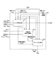
図4は、第1の実施の形態における信号処理チップ300の一構成例を示すブロック図である。この信号処理チップ300は、PLLブロック310、分周器ブロック320、故障検知部330、信号処理部400および復帰処理部410を備える。
[Configuration example of signal processing chip]
FIG. 4 is a block diagram illustrating a configuration example of the
PLLブロック310は、クロック信号CLKXtalを逓倍するものである。このPLLブロック310は、逓倍した信号をクロック信号CLKPLLとして分周器ブロック320に供給する。
The
分周器ブロック320は、クロック信号CLKPLLを分周するものである。この分周器ブロック320は、分周した信号をクロック信号CLKDIVとして故障検知部330および信号処理部400に供給する。このクロック信号CLKDIVは、3つのクロック信号を含み、3本の信号線を介して伝送される。図4では、記載の便宜上、この3本の信号線を1本にまとめて記載している。
The
信号処理部400は、画像データに対して所定の信号処理を行うものである。この信号処理部400は、CDS(Correlated Double Sampling)処理、ホワイトバランス処理および合成処理などの複数の信号処理を行う。合成処理としては、3次元ノイズリダクションやワイドダイナミックレンジ合成などが実行される。それぞれの信号処理は、クロック信号CLKIMGやクロック信号CLKDIVに同期して実行される。信号処理部400は、信号処理後の画像データをバックエンドチップ120に供給する。
The
故障検知部330は、車載カメラ100において生じた故障を検知するものである。この故障検知部330は、所定の検知タイミングにおいて、クロック信号CLKXtal、CLKPLL、CLKDIVおよびCLKIMGに基づいて、監視対象のブロックのそれぞれについて故障を検知する。監視対象のブロックは、例えば、水晶発振器110、撮像素子200、PLLブロック310および分周器ブロック320である。故障検知部330は、監視対象のブロックごとに、故障の有無を示す故障フラグを生成し、復帰処理部410に供給する。
The
復帰処理部410は、故障個所を復帰する処理を行うものである。この復帰処理部410の機能は、例えば、CPU(Central Processing Unit)がプログラムを実行することにより実現される。また、復帰処理部410は、ステータス情報を生成してバックエンドチップ120に供給する。
The
[PLLブロックの構成例]
図5は、第1の実施の形態におけるPLLブロック310の一構成例を示すブロック図である。このPLLブロック310は、予備PLL311、主PLL312、レジスタ313およびセレクタ314を備える。
[Configuration example of PLL block]
FIG. 5 is a block diagram illustrating a configuration example of the PLL block 310 according to the first embodiment. The
レジスタ313は、分周比NPLLを保持するものである。この分周比NPLLは、所定の実数であり、復帰処理部410から供給される。
The
予備PLL311は、クロック信号CLKXtalを逓倍するものである。この予備PLL311は、レジスタ313から分周比NPLLを読み出し、クロック信号CLKXtalを逓倍比1/NPLLで逓倍してクロック信号CLKPLL_Sを生成する。そして、予備PLL311は、クロック信号CLKPLL_Sをセレクタ314に供給する。なお、予備PLL311は、特許請求の範囲に記載の予備回路の一例である。
The
主PLL312は、クロック信号CLKXtalを逓倍するものである。この主PLL312は、レジスタ313から分周比NPLLを読み出し、クロック信号CLKXtalを逓倍比1/NPLLで逓倍してクロック信号CLKPLL_Mを生成する。そして、主PLL312は、クロック信号CLKPLL_Mをセレクタ314に供給する。なお、主PLL312は、特許請求の範囲に記載の第2の周期信号生成部の一例である。
The
セレクタ314は、クロック信号CLKPLL_Mとクロック信号CLKPLL_Sとのいずれかを、復帰処理部410からの選択信号SELPLLに従って選択するものである。このセレクタ314は、選択した信号をクロック信号CLKPLLとして分周器ブロック320に供給する。
The
[分周器ブロックの構成例]
図6は、第1の実施の形態における分周器ブロック320の一構成例を示すブロック図である。この分周器ブロック320は、主分周器321、322および323と、予備分周器324と、レジスタ326と、セレクタ325、327、328および329とを備える。
[Configuration example of divider block]
FIG. 6 is a block diagram illustrating a configuration example of the
レジスタ326は、分周比NDIV1、NDIV2およびNDIV3を保持するものである。これらの分周比は、所定の実数であり、復帰処理部410から供給される。なお、分周比NDIV1、NDIV2およびNDIV3を1つのレジスタ326に保持させているが、これらを複数のレジスタに分散して保持させてもよい。
The
主分周器321は、クロック信号CLKPLLを分周するものである。この主分周器321は、レジスタ326から分周比NDIV1を読み出し、その分周比でクロック信号CLKPLLを分周してクロック信号CLKDIV1_Mを生成する。そして、主分周器321は、クロック信号CLKDIV1_Mをセレクタ327に供給する。なお、主分周器321は、特許請求の範囲に記載の第1の周期信号生成部の一例である。
The
主分周器322は、分周比NDIV2により分周する点以外は、主分周器321と同様である。この主分周器322は、分周した信号をクロック信号CLKDIV2_Mとしてセレクタ328に供給する。なお、主分周器322は、特許請求の範囲に記載の第2の周期信号生成部の一例である。
The
主分周器323は、分周比NDIV3により分周する点以外は、主分周器321と同様である。この主分周器323は、分周した信号をクロック信号CLKDIV3_Mとしてセレクタ329に供給する。なお、主分周器323は、特許請求の範囲に記載の第3の周期信号生成部の一例である。
The
予備分周器324は、セレクタ325からの分周比により分周する点以外は、主分周器321と同様である。この予備分周器324は、分周した信号をクロック信号CLKDIV_Sとしてセレクタ327、328および329に供給する。なお、予備分周器324は、特許請求の範囲に記載の予備回路の一例である。
The
セレクタ325は、復帰処理部410からの選択信号SELDIV_Sに従って分周比NDIV1、NDIV2およびNDIV3のいずれかを予備分周器324に供給するものである。
The
セレクタ327は、復帰処理部410からの選択信号SELDIV1に従ってクロック信号CLKDIV1_Mとクロック信号CLKDIV_Sとのいずれかを選択するものである。このセレクタ327は、選択した信号をクロック信号CLKDIV1として故障検知部330および信号処理部400に出力する。
The
セレクタ328は、復帰処理部410からの選択信号SELDIV2に従ってクロック信号CLKDIV2_Mとクロック信号CLKDIV_Sとのいずれかを選択するものである。このセレクタ328は、選択した信号をクロック信号CLKDIV2として故障検知部330等に出力する。
The
セレクタ329は、復帰処理部410からの選択信号SELDIV3に従ってクロック信号CLKDIV3_Mとクロック信号CLKDIV_Sとのいずれかを選択するものである。このセレクタ329は、選択した信号をクロック信号CLKDIV3として故障検知部330等に出力する。
The
[故障検知部の構成例]
図7は、第1の実施の形態における故障検知部330の一構成例を示すブロック図である。この故障検知部330は、PLL群故障検知部340および分周器ブロック故障検知部360を備える。
[Configuration example of failure detection unit]
FIG. 7 is a block diagram illustrating a configuration example of the
PLL群故障検知部340は、PLLブロック310、撮像素子200および水晶発振器110のそれぞれについて故障を検知するものである。このPLL群故障検知部340は、クロック信号CLKXtal、CLKPLLおよびCLKIMGから故障フラグF_PLL、F_IMGおよびF_Xtalを生成して復帰処理部410に供給する。ここで、故障フラグF_PLLは、PLLブロック310の故障の有無を示す。また、故障フラグF_IMGは、撮像素子200の故障の有無を示し、故障フラグF_Xtalは、水晶発振器110の故障の有無を示す。
The PLL group
分周器ブロック故障検知部360は、分周器ブロック320内の主分周器321、322および323のそれぞれについて故障を検知するものである。この分周器ブロック故障検知部360は、クロック信号CLKDIV1、CLKDIV2およびCLKDIV3から故障フラグF_DIV1、F_DIV2およびF_DIV3を生成して復帰処理部410に供給する。ここで、故障フラグF_DIV1は、主分周器321の故障の有無を示す。また、故障フラグF_DIV2は、主分周器322の故障の有無を示し、故障フラグF_DIV3は、主分周器323の故障の有無を示す。
The frequency divider block
[PLL群故障検知部の構成例]
図8は、第1の実施の形態におけるPLL群故障検知部340の一構成例を示すブロック図である。このPLL群故障検知部340は、カウンタ341、342および343と、比率判定ブロック344と、故障個所特定部351とを備える。
[Configuration example of PLL group failure detection unit]
FIG. 8 is a block diagram illustrating a configuration example of the PLL group
カウンタ341は、水晶発振器110からのクロック信号CLKXtalに同期して計数値CNTXtalを計数するものである。このカウンタ341は、計数値CNTXtalを比率判定ブロック344に供給する。なお、カウンタ341は、特許請求の範囲に記載の第1のカウンタの一例である。
The
カウンタ342は、PLLブロック310からのクロック信号CLKPLLに同期して計数値CNTPLLを計数するものである。このカウンタ342は、計数値CNTPLLを比率判定ブロック344に供給する。なお、カウンタ342は、特許請求の範囲に記載の第2のカウンタの一例である。
The
カウンタ343は、撮像素子200からのクロック信号CLKIMGに同期して計数値CNTIMGを計数するものである。このカウンタ343は、計数値CNTIMGを比率判定ブロック344に供給する。なお、カウンタ343は、特許請求の範囲に記載の第3のカウンタの一例である。
The
また、カウンタ341、342および343は、復帰処理部410により生成されたリセット信号RST1が入力されると、計数値を初期値にする。この初期化のタイミングは、設計者や使用者により任意に設定することができる。例えば、前述の検知イネーブルEN_D1に連動して、復帰処理部410によりリセット信号RST1が生成される。
Further, when the reset signal RST1 generated by the
比率判定ブロック344は、計数値CNTXtalおよびCNTPLLの組と、計数値CNTPLLおよびCNTIMGの組と、計数値CNTIMGおよびCNTXtalの組とのそれぞれについて、比率が略一定値であるか否かを判定するものである。この比率判定ブロック344は、比率判定部345、346および347を備える。
The
比率判定部345は、所定のタイミング(計数値CNTXtalが設定値C1であるタイミングなど)において、計数値CNTXtalと計数値CNTPLLとの比率が略一定値であるか否かを判定するものである。
The
例えば、比率判定部345は、CNTPLL/CNTXtalが(C2/C1)±α1の範囲内であるか(すなわち、略一定値である)か否かを判定する。比率判定部345は、判定結果を示す判定フラグF_PLL・Xtalを故障個所特定部351に供給する。この判定フラグF_PLL・Xtalは、クロック信号CLKPLLとクロック信号CLKXtalとの周波数の比率が略一定値であるか否かを示す。この比率が略一定値でない場合には、水晶発振器110またはPLLブロック310の停止や、それらの生成する周波数の関係が崩れていることが想定される。このため、水晶発振器110およびPLLブロック310のいずれかの故障として扱われる。
For example, the
設定値C1およびC2には、それらの比率がPLLブロック310の逓倍比1/NPLLとなる値が設定される。例えば、逓倍比1/NPLLが「5」である場合、C2/C1が「5」となる値が設定される。
In the setting values C1 and C2, a value is set such that the ratio thereof becomes the
比率判定部346は、所定のタイミングにおいて、計数値CNTXtalと計数値CNTIMGとの比率が略一定値であるか否かを判定するものである。
The
例えば、比率判定部346は、CNTIMG/CNTXtalが(C4/C3)±α2の範囲内であるかか否かを判定する。比率判定部346は、判定結果を示す判定フラグF_IMG・Xtalを故障個所特定部351に供給する。この判定フラグF_IMG・Xtalは、クロック信号CLKIMGとクロック信号CLKXtalとの周波数の比率が略一定値であるか否かを示す。比率が略一定値でない場合には、水晶発振器110および撮像素子200のいずれかの故障が推測される。
For example, the
設定値C3およびC4には、それらの比率が撮像素子200の逓倍比1/NIMGとなる値が設定される。
In the setting values C3 and C4, a value is set such that the ratio thereof becomes the
比率判定部347は、所定のタイミングにおいて、計数値CNTPLLと計数値CNTIMGとの比率が略一定値であるか否かを判定するものである。
The
例えば、比率判定部347は、CNTPLL/CNTIMGが(C6/C5)±α3の範囲内であるかか否かを判定する。比率判定部347は、判定結果を示す判定フラグF_PLL・IMGを故障個所特定部351に供給する。この判定フラグF_PLL・IMGは、クロック信号CLKPLLとクロック信号CLKIMGとの周波数の比率が略一定値であるか否かを示す。比率が略一定値でない場合には、PLLブロック310および撮像素子200のいずれかの故障が推測される。
For example, the
設定値C5およびC6には、それらの比率が、故障が無い理想的な状態のクロック信号CLKIMGおよびCLKPLLの周波数の比率となる値が設定される。例えば、理想的な状態のクロック信号CLKIMGの周波数が10メガヘルツ(MHz)で、クロック信号CLKPLLの周波数が20メガヘルツ(MHz)である場合、C6/C5が「2」となる値が設定される。なお、理想的なクロック信号CLKIMGおよびCLKPLLの周波数が同一である場合には、C5およびC6のいずれかが比率判定部347に共通に設定される。
The set values C5 and C6 are set to values that are ratios of the frequencies of the clock signals CLK IMG and CLK PLL in an ideal state with no failure. For example, when the frequency of the clock signal CLK IMG in an ideal state is 10 megahertz (MHz) and the frequency of the clock signal CLK PLL is 20 megahertz (MHz), C6 / C5 is set to a value “2”. The If ideal clock signals CLK IMG and CLK PLL have the same frequency, one of C5 and C6 is set in common in
故障個所特定部351は、水晶発振器110、PLLブロック310および撮像素子200のいずれかに故障が生じた際に故障個所を特定するものである。この故障個所特定部351には、復帰処理部410により生成された検知イネーブルEN_D1が入力される。この検知イネーブルEN_D1は、故障個所特定部351を動作させるか否かを示す信号である。故障の検知を行うタイミングにおいて検知イネーブルEN_D1にイネーブルが設定される。
The failure
検知イネーブルEN_D1がイネーブルである場合に故障個所特定部351は、3つの判定フラグから故障フラグF_PLL、F_IMGおよびF_Xtalを生成して復帰処理部410に供給する。
When the detection enable EN_D1 is enabled, the failure
図9は、第1の実施の形態におけるPLL群故障検知部内の故障個所特定部351の動作の一例を示す図である。検知イネーブルEN_D1が「0」(ディセーブル)である場合に故障個所特定部351は、故障フラグF_PLL、F_IMGおよびF_Xtalを全て「0」(故障無し)にする。
FIG. 9 is a diagram illustrating an example of the operation of the failure
また、検知イネーブルEN_D1が「1」(イネーブル)で、判定フラグが全て「0」である場合に故障個所特定部351は、故障フラグF_PLL、F_IMGおよびF_Xtalを全て「0」(故障無し)にする。
Further, when the detection enable EN_D1 is “1” (enable) and the determination flags are all “0”, the failure
ここで、判定フラグには、監視対象の一対のクロック信号の周波数の比率が略一定である場合に「0」が設定され、そうでない場合に「1」が設定されるものとする。また、水晶発振器110、撮像素子200およびPLLブロック310は、同時に2つ以上が故障しないものとする。
Here, the determination flag is set to “0” when the ratio of the frequencies of the pair of clock signals to be monitored is substantially constant, and is set to “1” otherwise. Further, it is assumed that two or more of the
検知イネーブルEN_D1が「1」で、判定フラグF_PLL・XtalおよびF_PLL・IMGのみが「1」である場合に故障個所特定部351は、故障フラグF_PLLのみを「1」(故障有り)にする。
When the detection enable EN_D1 is “1” and only the determination flags F_PLL · Xtal and F_PLL · IMG are “1”, the failure
前述したように判定フラグF_PLL・Xtalが「1」の場合には水晶発振器110およびPLLブロック310のいずれかの故障が推測される。また、判定フラグF_PLL・IMGが「1」の場合にはPLLブロック310および撮像素子200のいずれかの故障が推測される。したがって、故障個所特定部351は、それらの判定フラグに共通するPLLブロック310において故障が生じていると判断することができる。
As described above, when the determination flag F_PLL · Xtal is “1”, a failure of either the
また、検知イネーブルEN_D1が「1」で、判定フラグF_IMG・XtalおよびF_PLL・IMGのみが「1」である場合に故障個所特定部351は、故障フラグF_IMGのみを「1」(故障有り)にする。検知イネーブルEN_D1が「1」で、判定フラグF_PLL・XtalおよびF_IMG・Xtalのみが「1」である場合に故障個所特定部351は、故障フラグF_Xtalのみを「1」(故障有り)にする。
Further, when the detection enable EN_D1 is “1” and only the determination flags F_IMG · Xtal and F_PLL · IMG are “1”, the failure
このように、監視対象の3つのブロックのうち2つ以上が同時に故障しないと仮定すると、いずれか1つの回路が故障した際に、その故障個所に対応する2つの判定フラグが「1」になり、残りの判定フラグは「0」になる。このため、故障個所特定部351は、「1」になった2つの判定フラグの組合せから故障個所を特定することができる。なお、PLL群故障検知部340は、3つの判定フラグから3つのブロックの中の故障個所を特定しているが、4つ以上の判定フラグから4つ以上のブロックの中の故障個所を特定してもよい。分周器ブロック故障検知部360についても同様である。
As described above, assuming that two or more of the three blocks to be monitored do not fail at the same time, when any one of the circuits fails, the two determination flags corresponding to the failure location become “1”. The remaining determination flags are “0”. Therefore, the failure
[分周器ブロック故障検知部の構成例]
図10は、第1の実施の形態における分周器ブロック故障検知部360の一構成例を示すブロック図である。この分周器ブロック故障検知部360は、カウンタ361、362および363と、比率判定ブロック364および故障個所特定部365を備える。
[Configuration example of divider block failure detection unit]
FIG. 10 is a block diagram illustrating a configuration example of the frequency divider block
カウンタ361は、分周器ブロック320からのクロック信号CLKDIV1に同期して計数値CNTDIV1を計数するものである。このカウンタ361は、計数値CNTDIV1を比率判定ブロック364に供給する。なお、カウンタ361は、特許請求の範囲に記載の第1のカウンタの一例である。
The
カウンタ362は、分周器ブロック320からのクロック信号CLKDIV2に同期して計数値CNTDIV2を計数するものである。このカウンタ362は、計数値CNTDIV2を比率判定ブロック364に供給する。なお、カウンタ362は、特許請求の範囲に記載の第2のカウンタの一例である。
The
カウンタ363は、分周器ブロック320からのクロック信号CLKDIV3に同期して計数値CNTDIV3を計数するものである。このカウンタ363は、計数値CNTDIV3を比率判定ブロック364に供給する。なお、カウンタ363は、特許請求の範囲に記載の第3のカウンタの一例である。
The
また、カウンタ361、362および363は、復帰処理部410により生成されたリセット信号RST2が入力されると、計数値を初期値にする。例えば、前述の検知イネーブルEN_D2に連動して、復帰処理部410によりリセット信号RST2が生成される。
In addition, when the reset signal RST2 generated by the
比率判定ブロック364は、計数値CNTDIV1およびCNTDIV2の組と、計数値CNTDIV2およびCNTDIV3の組と、計数値CNTDIV1およびCNTDIV3の組とのそれぞれについて、比率が略一定値であるか否かを判定するものである。この比率判定ブロック364は、それぞれの判定結果を示す判定フラグF_DIV1・DIV2、F_DIV2・DIV3およびF_DIV1・DIV3を故障個所特定部365に供給する。
The
故障個所特定部365は、検知イネーブルEN_D2がイネーブルである場合に3つの判定フラグから故障フラグF_DIV1、F_DIV2およびF_DIV3を生成して復帰処理部410に供給する。
The failure
図11は、第1の実施の形態における分周器ブロック故障検知部360内の故障個所特定部365の動作の一例を示す図である。
FIG. 11 is a diagram illustrating an example of the operation of the failure
検知イネーブルEN_D2が「0」(ディセーブル)である場合に故障個所特定部365は、故障フラグF_DIV1、F_DIV2およびF_DIV3を全て「0」(故障無し)にする。
When the detection enable EN_D2 is “0” (disabled), the failure
また、検知イネーブルEN_D2が「1」(イネーブル)で、判定フラグが全て「0」である場合に故障個所特定部351は、故障フラグF_DIV1、F_DIV2およびF_DIV3を全て「0」(故障無し)にする。
When the detection enable EN_D2 is “1” (enable) and the determination flags are all “0”, the failure
検知イネーブルEN_D2が「1」で、判定フラグF_DIV1・DIV2およびF_DIV1・DIV3のみが「1」である場合に故障個所特定部351は、故障フラグF_DIV1のみを「1」(故障有り)にする。
When the detection enable EN_D2 is “1” and only the determination flags F_DIV1 and DIV2 and F_DIV1 and DIV3 are “1”, the failure
また、検知イネーブルEN_D2が「1」で、判定フラグF_DIV1・DIV2およびF_DIV2・DIV3のみが「1」である場合に故障個所特定部365は、故障フラグF_DIV2のみを「1」(故障有り)にする。検知イネーブルEN_D1が「1」で、判定フラグF_DIV2・DIV3およびF_DIV1・DIV3のみが「1」である場合に故障個所特定部365は、故障フラグF_DIV3のみを「1」(故障有り)にする。
Further, when the detection enable EN_D2 is “1” and only the determination flags F_DIV1 and DIV2 and F_DIV2 and DIV3 are “1”, the failure
このように、故障個所特定部365は、3つの判定フラグから分周器ブロック320内の3つの分周器のいずれに故障が生じたかを特定することができる。
As described above, the failure
図12は、第1の実施の形態における復帰処理部410の一構成例を示すブロック図である。この復帰処理部410は、レジスタ再設定部411、予備回路切替え制御部412およびステータス生成部413を備える。
FIG. 12 is a block diagram illustrating a configuration example of the
レジスタ再設定部411は、監視対象のブロックが故障した場合に、その故障個所のレジスタに設定値を再度保持させるものである。このレジスタ再設定部411は、所定のタイミングで検知イネーブルEN_D1およびEN_D2をイネーブルにして故障の検知を開始させる。また、故障の検知の開始時には、リセット信号RST1およびRST2により、カウンタがリセットされる。また、監視対象のクロック信号が非同期である場合も想定すると、その際には誤差が蓄積していくことが考えられる。このため、検知開始時に加えて、周波数の比率が略一定であるか否かが判定されるたびに、レジスタ再設定部411は、カウンタをリセットさせる。
When the monitoring target block fails, the
故障の検知は周期的に行われ、その周期PDETは、システムに影響が出ないような一定の閾値以内に設定される。例えば、周期PDETが、画像データ(フレーム)の撮像の周期内に収まるように設定される。例えば、周期PDETは、フレームの撮像周期の1/4程度に設定すれば、その撮像周期内に、故障の検知から復帰までの処理を完了することができる。周期PDETに対する閾値は、フレームの周期などに応じて、適宜、変更することができる。 Fault detection is performed periodically, and the period P DET is set within a certain threshold that does not affect the system. For example, the period P DET is set to fall within the imaging period of the image data (frame). For example, if the period P DET is set to about ¼ of the imaging period of the frame, the process from the detection of the failure to the return can be completed within the imaging period. The threshold for the period P DET can be appropriately changed according to the period of the frame.
ここで、前述したように撮像素子200内のレジスタには分周比NIMGが保持され、PLLブロック310内のレジスタには分周比NPLLが保持されている。また、分周器ブロック320内のレジスタには分周比NDIV1乃至NDIV3が保持されている。ブロックの故障の原因としては、ブロック内の回路の破損や配線の断線の他、ブロック内のレジスタのデータ化けが想定される。データ化けにより故障が生じた際には、そのレジスタに設定値を上書きずれば、故障から復帰する可能性がある。
Here, as described above, the frequency division ratio N IMG is held in the register in the
そこで、レジスタ再設定部411は、レジスタが設けられたブロックに対応する故障フラグF_IMG、F_PLL、F_DIV1、F_DIV2およびF_DIV3のいずれかが「1」である場合に、対応するレジスタに設定値を上書きする。レジスタ再設定部411は、故障フラグF_IMGが「1」の場合に分周比NIMGを撮像素子200に再度保持(上書き)させ、故障フラグF_PLLが「1」の場合に分周比NPLLをPLLブロック310に再度保持させる。また、故障フラグF_DIV1、F_DIV2およびF_DIV3のいずれかが「1」である場合にレジスタ再設定部411は、分周比NDIV1乃至NDIV3のうち、故障個所に係る分周比を分周器ブロック320に再度保持させる。
Accordingly, the
そして、レジスタ再設定部411は、レジスタ上書きの後に故障フラグを監視し、故障したブロックが故障から復帰したか否かを判断する。そして復帰した際にレジスタ再設定部411は、復帰確認通知R_REGをステータス生成部413に供給する。一方、復帰に失敗した際にレジスタ再設定部411は、復帰に失敗したブロックを予備回路切替え制御部412に通知して切替え制御を開始させる。
Then, the
予備回路切替え制御部412は、レジスタ上書きによる復帰が失敗した際に、故障したブロック内の主回路を予備回路に切り替える制御を行うものである。回路に故障が生じた際にレジスタ上書きを行っても復帰しない場合には、主回路の破損や配線の断線が生じている可能性がある。この場合には、主回路を予備回路に切り替えることにより復帰する可能性がある。
The spare circuit switching
そこで、予備回路切替え制御部412は、レジスタ上書きによるPLLブロック310の復帰に失敗した際に選択信号SELPLLにより主PLLを予備PLLに切り替える。また、レジスタ上書きによる分周器ブロック320の復帰に失敗した際に予備回路切替え制御部412は、選択信号SELDIV_SとSELDIV1乃至SELDIV3とにより、故障した主分周器を予備分周器に切り替える。
Therefore, the spare circuit switching
そして、予備回路切替え制御部412は、予備回路への切替え後に故障フラグF_PLLと故障フラグF_DIV1乃至F_DIV3とを監視して故障から復帰したか否かを判断する。そして、復帰した際に予備回路切替え制御部412は、復帰確認通知R_SELをステータス生成部413に供給する。
Then, the standby circuit switching
ステータス生成部413は、ステータス情報を生成するものである。このステータス情報は、監視対象のブロックのそれぞれのエラーステータスを含む。例えば、エラーステータスは、「正常」、「復帰中」および「故障中」に分類される。「正常」は、ブロックに故障が生じていない状態を示す。「復帰中」は、ブロックに対して復帰処理が実行されている状態を示す。「故障中」は、ブロックに、復帰不可能な故障が生じていることを示す。エラーステータスの初期状態は、「正常」に設定される。
The
ステータス生成部413は、復帰処理が可能なブロックに故障が生じた際に、そのブロックのステータスを「正常」から「復帰中」に遷移させる。そして、ステータス生成部413は、復帰処理の成否に応じて、ステータスを「復帰中」から「正常」または「故障中」に遷移させる。
When a failure occurs in a block that can be restored, the
一方、復帰処理が不可能なブロックに故障が生じた際に、ステータス生成部413は、そのブロックのステータスを「故障中」に遷移させる。例えば、水晶発振器110には、レジスタや予備回路が設けられていないため、復帰処理を行うことができない。このため、水晶発振器110に故障が生じた際には、そのステータスは「故障中」となる。
On the other hand, when a failure occurs in a block that cannot be restored, the
なお、車載カメラ100では、水晶発振器110、撮像素子200、PLLブロック310および分周器ブロック320を監視しているが、クロック信号などの周期信号を生成するブロックであれば、これら以外のブロックを監視してもよい。また、車載カメラ100は、水晶発振器110、撮像素子200、PLLブロック310および分周器ブロック320の全てを監視しているが、これらの一部のみを監視する構成であってもよい。
The in-
また、水晶発振器110および撮像素子200には予備回路を設けていないが、これらの少なくとも一方に予備回路を設けてもよい。また、撮像素子200、PLLブロック310および分周器ブロック320にレジスタを設けているが、これらの少なくとも1つにレジスタを設けない構成とすることもできる。また、PLLブロック310および分周器ブロック320の両方に予備回路を設けているが、これらの少なくとも一方に予備回路を設けない構成とすることもできる。それぞれのブロックにレジスタのみを設けるか、予備回路のみを設けるか、あるいはレジスタおよび予備回路の両方を設けるかは、そのブロックの重要性や安全性、コストなどを考慮して決定される。
Further, although no spare circuit is provided in the
また、復帰処理部410は、レジスタおよび予備回路の両方を設けたブロックに対してレジスタの上書きと、予備回路への切替えとの両方を行っているが、レジスタの上書きを行わない構成としてもよい。例えば、復帰処理の完了までの時間を短縮したい場合や、レジスタの信頼性が高く、データ化けが生じる可能性が低い場合であれば、予備回路への切替えのみを行う構成としてもよい。
In addition, the
図13は、第1の実施の形態におけるステータス情報のデータ構成の一例を示す図である。ステータス情報は、撮像素子200、PLLブロック310、分周器ブロック320内の3つの分周器、および、水晶発振器110のそれぞれのブロックのエラーステータスを含む。初期状態においては、全てのエラーステータスは「正常」に設定される。
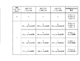
FIG. 13 is a diagram illustrating an example of a data configuration of status information according to the first embodiment. The status information includes an error status of each block of the
復帰処理が可能なブロック(例えば、PLLブロック310)で故障が生じた際には、復帰処理部410は、レジスタ上書きや、予備回路への切替えを含む復帰処理を行う。復帰処理中は、そのブロックのステータスは「復帰中」に設定される。復帰に失敗したブロックのステータスには、「故障中」が設定される。
When a failure occurs in a block that can be restored (for example, the PLL block 310), the
水晶発振器110に故障が生じた際には、バックエンドチップ120は、車載カメラ100全体の故障としてアラーム信号を出力する。
When a failure occurs in the
なお、ステータス情報の構成は、図13に例示したものに限定されない。復帰処理部410は、例えば、ブロックごとに、故障フラグと復帰確認通知とを含むステータス情報を生成してもよい。
The configuration of the status information is not limited to that illustrated in FIG. For example, the
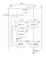
図14は、第1の実施の形態における復帰処理部410の動作の一例を示す図である。この動作は、例えば、車載カメラ100に電源が投入されたときに開始される。復帰処理部410は、検知タイミングにおいて故障フラグを参照して、いずれかのブロックに故障があるか否かを判断する(ステップS901)。
FIG. 14 is a diagram illustrating an example of the operation of the
いずれかのブロックに故障がある場合に(ステップS901:Yes)、復帰処理部410は、水晶発振器110が故障したか否かを判断する(ステップS902)。故障個所が水晶発振器110でない場合に(ステップS902:No)、復帰処理部410は、そのブロックが復帰中である旨をステータス情報によりバックエンドチップ120に通知する(ステップS903)。そして、復帰処理部410は、故障したブロックのレジスタの上書きを行う(ステップS904)。
When any block has a failure (step S901: Yes), the
レジスタ上書きの後に復帰処理部410は、上書きを行ったブロックの故障フラグを監視し、故障の有無を判断する(ステップS905)。故障がある場合に(ステップS905:Yes)、復帰処理部410は、故障が生じたブロックに予備回路があるか否かを判断する(ステップS906)。予備回路が有る場合に(ステップS906:Yes)、復帰処理部410は、その予備回路への切替えを行う(ステップS907)。
After register overwriting, the
予備回路への切替えの後に復帰処理部410は、切替えを行ったブロックの故障フラグを監視し、故障の有無を判断する(ステップS908)。水晶発振器110が故障した場合(ステップS902:Yes)、予備回路が無い場合(ステップS906:No)、または、切替え後に故障がある場合(ステップS908:Yes)、復帰処理部410は、ブロックが故障中である旨を通知する(ステップS909)。
After switching to the spare circuit, the
一方、上書き後に故障が無い場合(ステップS905:Yes)、または、切替え後に故障が無い場合(ステップS908:No)、復帰処理部410は、ブロックが正常中である旨を通知する(ステップS910)。全てのブロックに故障がない場合に(ステップS901:No)、または、ステップS910の後に復帰処理部410は、ステップS901以降を繰り返し実行する。
On the other hand, when there is no failure after overwriting (step S905: Yes), or when there is no failure after switching (step S908: No), the
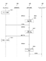
図15は、第1の実施の形態における撮像素子200が故障した際の車載カメラ100の動作の一例を示すシーケンス図である。故障検知部330は、撮像素子200の故障を検知し、故障フラグにより復帰処理部410に通知する。復帰処理部410は、復帰中をバックエンドチップ120に通知するとともに、撮像素子200に分周比を供給して、レジスタの上書き制御を行う(ステップS904)。
FIG. 15 is a sequence diagram illustrating an example of the operation of the in-
そして、レジスタの上書き後に故障検知部330が撮像素子200の故障を検知すると、復帰処理部410は、撮像素子200が故障中である旨をバックエンドチップ120に通知する(ステップS909)。
When the
このように、故障したブロックにレジスタがある場合に復帰処理部410は、そのレジスタの上書きにより復帰を試みる。
As described above, when there is a register in the failed block, the
図16は、第1の実施の形態におけるPLLブロック310が故障した際の車載カメラの動作の一例を示すシーケンス図である。初期状態のPLLブロック310において、主PLLが、クロック信号CLKXtalを逓倍してクロック信号CLKPLLを生成する(ステップS911)。
FIG. 16 is a sequence diagram illustrating an example of the operation of the in-vehicle camera when the
そして、PLLブロック310で故障が生じると、故障検知部330は、PLLブロック310の故障を復帰処理部410に通知する。復帰処理部410は、復帰中をバックエンドチップ120に通知するとともに、PLLブロック310に分周比を供給して、レジスタの上書き制御を行う(ステップS904)。
When a failure occurs in the
そして、レジスタの上書き後に故障検知部330がPLLブロック310の故障を検知すると、復帰処理部410は、PLLブロック310に選択信号を供給して予備回路への切替え制御を行う(ステップS907)。PLLブロック310は、選択信号に従って予備PLLに切り替える(ステップS912)。
When the
予備PLLへの切替え後に故障検知部330がPLLブロック310の故障を検知すると、復帰処理部410は、PLLブロック310が故障中である旨をバックエンドチップ120に通知する(ステップS909)。
When the
上述したように故障したブロックにレジスタおよび予備回路の両方がある場合に復帰処理部410は、レジスタの上書きにより復帰を試み、復帰できなければ予備回路への切替えを行う。
As described above, when both the register and the spare circuit exist in the failed block, the
このように、本技術の第1の実施の形態によれば、車載カメラ100は、一対のクロック信号の周波数の比率が略一定であるか否かを示す3つの判定フラグから故障個所を特定するため、クロック信号を生成する回路の故障の状態を正確に判断することができる。
As described above, according to the first embodiment of the present technology, the in-
[変形例]
上述の第1の実施の形態では、予備回路への切替え前に予備回路の故障を検知していなかった。ここで、故障を検知するには前述したようにカウンタにより一定期間計数する必要がある。このため、切替え前に予備回路が既に故障していた場合には、切替え後の一定期間後に、その予備回路の故障を検知して復帰処理を終了することとなり、復帰処理の終了までの時間が長くなる問題がある。この第1の実施の形態の変形例の車載カメラ100は、復帰処理の終了までの時間を短くする点において第1の実施の形態と異なる。
[Modification]
In the first embodiment described above, failure of the spare circuit is not detected before switching to the spare circuit. Here, in order to detect a failure, it is necessary to count for a certain period with a counter as described above. For this reason, if the spare circuit has already failed before switching, the failure of the spare circuit is detected after a certain period after switching, and the restoration process is terminated. There is a problem that becomes longer. The in-
図17は、第1の実施の形態の変形例における分周器ブロック320の一構成例を示すブロック図である。この変形例の分周器ブロック320は、予備分周器324が、クロック信号CLKDIV_Sを、セレクタ327、328および329の他、故障検知部330にも供給する点において第1の実施の形態と異なる。
FIG. 17 is a block diagram illustrating a configuration example of the
図18は、第1の実施の形態の変形例における分周器ブロック故障検知部360の一構成例を示すブロック図である。この変形例の分周器ブロック故障検知部360は、比率判定ブロック364および故障個所特定部365の代わりに、比率判定ブロック372および故障個所特定部373を備え、カウンタ371をさらに備える点において第1の実施の形態と異なる。
FIG. 18 is a block diagram illustrating a configuration example of the frequency divider block
カウンタ371は、分周器ブロック320からのクロック信号CLKDIV_Sに同期して計数値CNTDIVSを計数するものである。このカウンタ371は、計数値CNTDIVSを比率判定ブロック372に供給する。また、カウンタ371は、リセット信号RST2が入力されると、計数値を初期値にする。例えば、前述の検知イネーブルEN_D2に連動して、復帰処理部410によりリセット信号RST2が生成される。
The
比率判定ブロック372は、4つの計数値から判定フラグF_DIV1・DIV2、F_DIV2・DIV3およびF_DIV1・DIV3、F_DIV1・DIVSおよびF_DIV1・DIVSを生成して故障個所特定部373に供給する。ここで、判定フラグF_DIV1・DIVSは、計数値CNTDIV1と計数値CNTDIVSとの比率が略一定であるか否かを示し、判定フラグF_DIV2・DIVSは、計数値CNTDIV2と計数値CNTDIVSとの比率が略一定であるか否かを示す。なお、比率判定ブロック372はCNTDIV1およびCNTDIV2とCNTDIVSとから2つの判定フラグを生成しているが、CNTDIV1およびCNTDIV2以外の組合せの2つの計数値とCNTDIVSとから2つの判定フラグを生成してもよい。
The
故障個所特定部373は、5つの判定フラグから故障フラグF_DIV1、F_DIV2、F_DIV3およびF_DIVSを生成して復帰処理部410に供給する。故障フラグF_DIVSは、予備分周器が故障しているか否かを示す。例えば、判定フラグF_DIV1・DIVSおよびF_DIV2・DIVSが両方とも「1」の場合に故障フラグF_DIVSに「1」が設定される。
The failure
復帰処理部410は、予備分周器への切替え前に故障フラグF_DIVSを参照し、予備回路が故障していなければ、切替えを行う。一方、予備分周器が故障していれば、復帰処理部410は、切替えを行わずに、対応する分周器のステータスを「故障中」にして復帰処理を終了する。これにより、切替え前に予備回路が故障していた際に、復帰処理の終了までの時間を短くすることができる。
The
なお、故障検知部330は、PLLブロック310内の予備PLLが故障しているか否かを検知していないが、分周器ブロック320と同様に、予備PLLについても故障を検知してもよい。
Note that the
図19は、第1の実施の形態の変形例における復帰処理部410の動作の一例を示す図である。この変形例の復帰処理部410の動作は、ステップS911をさらに実行する点において第1の実施の形態と異なる。
FIG. 19 is a diagram illustrating an example of the operation of the
復帰処理部410は、故障ブロックに予備回路がある場合に(ステップS906:Yes)、予備回路が故障中であるか否かを判断する(ステップS911)。予備回路が故障してない場合に(ステップS911:No)、復帰処理部410は、予備回路への切替えを行う(ステップS907)。一方、予備回路が故障中の場合に(ステップS908:Yes)、復帰処理部410は、そのブロックが故障中である旨を通知する(ステップS909)。
When there is a spare circuit in the failed block (step S906: Yes), the
このように、本技術の第1の実施の形態の変形例によれば、車載カメラ100は、予備分周器が故障しているか否かを判断し、故障していなければ切り替えるため、復帰処理の終了までの時間を短くすることができる。
As described above, according to the modification of the first embodiment of the present technology, the in-
<2.第2の実施の形態>
上述の第1の実施の形態では、信号処理チップ300は画像データとステータス情報とを別々に供給していた。しかし、この構成では、画像データを送信する信号線309と別途にステータス情報を送信する信号線308を配線する必要があり、配線数が増大する。また、画像データのみを送信する場合と比較して、ステータス情報の分、信号処理チップ300とバックエンドチップ120との間の通信量が増大してしまうおそれがある。この第2の実施の形態の車載カメラ100は、チップ間の配線数や通信量を削減した点において第1の実施の形態と異なる。
<2. Second Embodiment>
In the first embodiment described above, the
図20は、第2の実施の形態における信号処理チップ300の一構成例を示すブロック図である。この第2の実施の形態の信号処理チップ300は、ステータス重畳部420をさらに備える点において第1の実施の形態と異なる。ステータス重畳部420は、ステータス情報を画像データに重畳してバックエンドチップ120に供給するものである。なお、ステータス重畳部420は、特許請求の範囲に記載の重畳部の一例である。
FIG. 20 is a block diagram illustrating a configuration example of the
図21は、第2の実施の形態における画像データのデータ構成の一例を示す図である。MIPI(Mobile Industry Processor Interface alliance)規格において画像データの先頭には例えば、SOF(Start of Frame)が配置される。また、画像データの末尾にはEOF(End of Frame)が配置される。画像データは複数のラインを含む。ラインのそれぞれの先頭にはPH(Packet Header)が配置され、末尾にはPF(Packet Footer)が配置される。また、これらのラインは、有効画像データ出力ラインと、エンベデッドデータ出力ライン(FrameInfoLine)とに分類される。このFrameInfoLineには画像データに関連する各種の情報が格納される。ステータス情報は、例えば、このFrameInfoLineに格納される。なお、ステータス情報を格納することができるのであれば、画像データの構成は、同図に例示したものに限定されない。 FIG. 21 is a diagram illustrating an example of a data configuration of image data according to the second embodiment. In the MIPI (Mobile Industry Processor Interface alliance) standard, for example, SOF (Start of Frame) is arranged at the head of image data. An EOF (End of Frame) is arranged at the end of the image data. The image data includes a plurality of lines. A PH (Packet Header) is disposed at the head of each line, and a PF (Packet Footer) is disposed at the end of each line. These lines are classified into an effective image data output line and an embedded data output line (FrameInfoLine). In the FrameInfoLine, various types of information related to image data are stored. The status information is stored in, for example, this FrameInfoLine. As long as status information can be stored, the configuration of the image data is not limited to that illustrated in FIG.
図22は、第2の実施の形態におけるステータス情報の格納場所の一例を示す図である。FrameInfoLineにおいて、1番目の画素の位置にデータ数が格納され、2番目の画素の位置にフレームカウントが格納される。そして、3番目の画素の位置にステータス情報が格納される。 FIG. 22 is a diagram illustrating an example of a storage location of status information according to the second embodiment. In FrameInfoLine, the number of data is stored at the position of the first pixel, and the frame count is stored at the position of the second pixel. Status information is stored at the position of the third pixel.
このように、本技術の第2の実施の形態によれば、信号処理チップ300は、画像データにステータス情報を重畳してバックエンドチップ120に供給するため、重畳しない場合と比較してチップ間の配線数や通信量を削減することができる。
As described above, according to the second embodiment of the present technology, the
なお、上述の実施の形態は本技術を具現化するための一例を示したものであり、実施の形態における事項と、特許請求の範囲における発明特定事項とはそれぞれ対応関係を有する。同様に、特許請求の範囲における発明特定事項と、これと同一名称を付した本技術の実施の形態における事項とはそれぞれ対応関係を有する。ただし、本技術は実施の形態に限定されるものではなく、その要旨を逸脱しない範囲において実施の形態に種々の変形を施すことにより具現化することができる。 The above-described embodiment shows an example for embodying the present technology, and the matters in the embodiment and the invention-specific matters in the claims have a corresponding relationship. Similarly, the invention specific matter in the claims and the matter in the embodiment of the present technology having the same name as this have a corresponding relationship. However, the present technology is not limited to the embodiment, and can be embodied by making various modifications to the embodiment without departing from the gist thereof.
また、上述の実施の形態において説明した処理手順は、これら一連の手順を有する方法として捉えてもよく、また、これら一連の手順をコンピュータに実行させるためのプログラム乃至そのプログラムを記憶する記録媒体として捉えてもよい。この記録媒体として、例えば、CD(Compact Disc)、MD(MiniDisc)、DVD(Digital Versatile Disc)、メモリカード、ブルーレイディスク(Blu-ray(登録商標)Disc)等を用いることができる。 Further, the processing procedure described in the above embodiment may be regarded as a method having a series of these procedures, and a program for causing a computer to execute these series of procedures or a recording medium storing the program. You may catch it. As this recording medium, for example, a CD (Compact Disc), an MD (MiniDisc), a DVD (Digital Versatile Disc), a memory card, a Blu-ray disc (Blu-ray (registered trademark) Disc), or the like can be used.
なお、ここに記載された効果は必ずしも限定されるものではなく、本開示中に記載されたいずれかの効果であってもよい。 Note that the effects described here are not necessarily limited, and may be any of the effects described in the present disclosure.
なお、本技術は以下のような構成もとることができる。
(1)第1の周期信号を生成する第1の周期信号生成部と、
前記第1の周期信号から第2の周期信号を生成する第2の周期信号生成部と、
前記第1の周期信号から第3の周期信号を生成する第3の周期信号生成部と、
前記第1および第2の前記周期信号の組と前記第2および第3の前記周期信号の組と前記第1および第3の前記周期信号の組とのそれぞれについて前記組内の一対の周期信号の周波数の比率が略一定であるか否かを判定する判定部と、
2つの前記組において前記比率が略一定でない場合には前記第1、第2および第3の周期信号生成部のうち前記2つの組に共通に含まれる周期信号に対応する周期信号生成部を故障個所として特定する故障個所特定部と
を具備する半導体装置。
(2)前記特定された故障個所を復帰させる復帰処理を行う復帰処理部をさらに具備する
前記(1)記載の半導体装置。
(3)少なくとも1つの前記組について当該組内の前記比率の設定値を保持するレジスタをさらに具備し、
前記第1、第2および第3の周期信号生成部の少なくとも1つは前記設定値に基づいて周期信号を生成し、
前記復帰処理は、前記レジスタに前記設定値を再度保持させる再設定処理を含む
前記(2)記載の半導体装置。
(4)予備周期信号を生成する予備回路をさらに具備し、
前記復帰処理は、前記第1、第2および第3の周期信号のうち前記故障個所に対応する周期信号の代わりに前記予備周期信号を前記判定部に出力させる切替え処理を含む
前記(3)記載の半導体装置。
(5)前記判定部は、前記第1、第2および第3の周期信号のうち複数の信号と前記予備周期信号との組について前記比率が略一定であるか否かをさらに判定し、
前記故障個所特定部は、前記第1、第2および第3の周期信号生成部と前記予備回路とのいずれかを前記故障個所として特定し、
前記復帰処理部は、前記予備回路が故障していない場合には前記第1、第2および第3の周期信号のうち前記故障個所に対応する周期信号の代わりに前記予備周期信号を前記判定部に出力させる
前記(4)記載の半導体装置。
(6)前記復帰処理部は、前記再設定処理の後に前記切替え処理を行う
前記(4)または(5)に記載の半導体装置。
(7)前記第1の周期信号に同期して第1の計数値を計数する第1のカウンタと、
前記第2の周期信号に同期して第2の計数値を計数する第2のカウンタと、
前記第3の周期信号に同期して第3の計数値を計数する第3のカウンタと
をさらに具備し、
前記判定部は、前記第1および第2の計数値の組と前記第2および第3の計数値の組と前記第1および第3の計数値の組のそれぞれについて前記組内の一対の計数値の比率が略一定値であるか否かを判定する
前記(1)から(6)のいずれかに記載の半導体装置。
(8)前記第1、第2および第3の周期信号のいずれかに同期して画像データを撮像する撮像部と、
前記特定された故障個所を示す情報を前記画像データに重畳する重畳部と
をさらに具備する
前記(1)から(7)のいずれかに記載の半導体装置。
(9)前記第1、第2および第3の周期信号生成部の少なくとも1つは、位相同期回路である
前記(1)から(8)のいずれかに記載の半導体装置。
(10)前記第1、第2および第3の周期信号生成部の少なくとも1つは、分周器である
前記(1)から(9)のいずれかに記載の半導体装置。
(11)前記第1、第2および第3の周期信号生成部の少なくとも1つは、水晶発振器である
前記(1)から(10)のいずれかに記載の半導体装置。
(12)前記第1および第2の前記周期信号の組と前記第2および第3の前記周期信号の組と前記第1および第3の前記周期信号の組とのそれぞれについて前記組内の一対の周期信号の周波数の比率が略一定であるか否かを判定する判定手順と、
2つの前記組において前記比率が略一定でない場合には前記第1、第2および第3の周期信号生成部のうち前記2つの組に共通に含まれる周期信号に対応する周期信号生成部を故障個所として特定する故障個所特定手順と
を具備する半導体装置の制御方法。
In addition, this technique can also take the following structures.
(1) a first periodic signal generator that generates a first periodic signal;
A second periodic signal generator for generating a second periodic signal from the first periodic signal;
A third periodic signal generator for generating a third periodic signal from the first periodic signal;
A pair of periodic signals in the set for each of the first and second sets of periodic signals, the second and third sets of periodic signals, and the first and third sets of periodic signals A determination unit for determining whether or not the frequency ratio is substantially constant;
If the ratio is not substantially constant in the two sets, the periodic signal generation unit corresponding to the periodic signal included in the two sets among the first, second, and third periodic signal generation units fails. A semiconductor device comprising a failure location identification unit identified as a location.
(2) The semiconductor device according to (1), further including a recovery processing unit that performs a recovery process for recovering the identified failure part.
(3) a register that holds a set value of the ratio in the set for at least one of the sets;
At least one of the first, second, and third periodic signal generators generates a periodic signal based on the set value;
The semiconductor device according to (2), wherein the return process includes a resetting process that causes the register to hold the setting value again.
(4) further comprising a spare circuit for generating a spare periodic signal;
The return process includes the switching process for causing the determination unit to output the preliminary periodic signal instead of the periodic signal corresponding to the failed part among the first, second, and third periodic signals. Semiconductor device.
(5) The determination unit further determines whether or not the ratio is substantially constant for a set of a plurality of signals and the backup periodic signal among the first, second, and third periodic signals,
The failure location specifying unit specifies any one of the first, second and third periodic signal generation units and the spare circuit as the failure location,
When the spare circuit is not out of order, the return processing unit uses the preliminary periodic signal instead of the periodic signal corresponding to the failed portion of the first, second, and third periodic signals as the determination unit. The semiconductor device according to (4), wherein the semiconductor device is output.
(6) The semiconductor device according to (4) or (5), wherein the return processing unit performs the switching process after the resetting process.
(7) a first counter that counts a first count value in synchronization with the first periodic signal;
A second counter for counting a second count value in synchronization with the second periodic signal;
A third counter for counting a third count value in synchronization with the third periodic signal,
The determination unit includes a pair of totals in the set for each of the set of the first and second count values, the set of the second and third count values, and the set of the first and third count values. The semiconductor device according to any one of (1) to (6), wherein it is determined whether or not a numerical value ratio is a substantially constant value.
(8) an imaging unit that captures image data in synchronization with any of the first, second, and third periodic signals;
The semiconductor device according to any one of (1) to (7), further including a superimposing unit that superimposes information indicating the identified failure location on the image data.
(9) The semiconductor device according to any one of (1) to (8), wherein at least one of the first, second, and third periodic signal generation units is a phase synchronization circuit.
(10) The semiconductor device according to any one of (1) to (9), wherein at least one of the first, second, and third periodic signal generation units is a frequency divider.
(11) The semiconductor device according to any one of (1) to (10), wherein at least one of the first, second, and third periodic signal generation units is a crystal oscillator.
(12) A pair in the set for each of the set of the first and second periodic signals, the set of the second and third periodic signals, and the set of the first and third periodic signals. A determination procedure for determining whether the frequency ratio of the periodic signal is substantially constant;
If the ratio is not substantially constant in the two sets, the periodic signal generation unit corresponding to the periodic signal included in the two sets among the first, second, and third periodic signal generation units fails. A method for controlling a semiconductor device, comprising: a failure location identification procedure that identifies a location.
100 車載カメラ
110 水晶発振器
120 バックエンドチップ
200 撮像素子
210 垂直走査回路
220 画素アレイ部
230 タイミング制御回路
240 カラムADC
250 水平走査回路
260、310 PLLブロック
261 PLL
262、313、326 レジスタ
270 出力部
300 信号処理チップ
311 予備PLL
312 主PLL
314、325、327、328、329 セレクタ
320 分周器ブロック
321、322、323 主分周器
324 予備分周器
330 故障検知部
340 PLL群故障検知部
341、342、343、361、362、363、371 カウンタ
344、364、372 比率判定ブロック
345、346、347 比率判定部
351、365、373 故障個所特定部
360 分周器ブロック故障検知部
400 信号処理部
410 復帰処理部
411 レジスタ再設定部
412 予備回路切替え制御部
413 ステータス生成部
420 ステータス重畳部
DESCRIPTION OF
250
262, 313, 326
312 Main PLL
314, 325, 327, 328, 329
Claims (12)
前記第1の周期信号から第2の周期信号を生成する第2の周期信号生成部と、
前記第1の周期信号から第3の周期信号を生成する第3の周期信号生成部と、
前記第1および第2の前記周期信号の組と前記第2および第3の前記周期信号の組と前記第1および第3の前記周期信号の組とのそれぞれについて前記組内の一対の周期信号の周波数の比率が略一定であるか否かを判定する判定部と、
2つの前記組において前記比率が略一定でない場合には前記第1、第2および第3の周期信号生成部のうち前記2つの組に共通に含まれる周期信号に対応する周期信号生成部を故障個所として特定する故障個所特定部と
を具備する半導体装置。 A first periodic signal generator for generating a first periodic signal;
A second periodic signal generator for generating a second periodic signal from the first periodic signal;
A third periodic signal generator for generating a third periodic signal from the first periodic signal;
A pair of periodic signals in the set for each of the first and second sets of periodic signals, the second and third sets of periodic signals, and the first and third sets of periodic signals A determination unit for determining whether or not the frequency ratio is substantially constant;
If the ratio is not substantially constant in the two sets, the periodic signal generation unit corresponding to the periodic signal included in the two sets among the first, second, and third periodic signal generation units fails. A semiconductor device comprising a failure location identification unit identified as a location.
請求項1記載の半導体装置。 The semiconductor device according to claim 1, further comprising a recovery processing unit that performs a recovery process for recovering the identified fault location.
前記第1、第2および第3の周期信号生成部の少なくとも1つは前記設定値に基づいて周期信号を生成し、
前記復帰処理は、前記レジスタに前記設定値を再度保持させる再設定処理を含む
請求項2記載の半導体装置。 A register that holds a set value of the ratio in the set for at least one set;
At least one of the first, second, and third periodic signal generators generates a periodic signal based on the set value;
The semiconductor device according to claim 2, wherein the return process includes a reset process for causing the register to hold the set value again.
前記復帰処理は、前記第1、第2および第3の周期信号のうち前記故障個所に対応する周期信号の代わりに前記予備周期信号を前記判定部に出力させる切替え処理を含む
請求項3記載の半導体装置。 A preliminary circuit for generating a preliminary periodic signal;
The return process includes a switching process for causing the determination unit to output the preliminary periodic signal instead of the periodic signal corresponding to the failed part among the first, second, and third periodic signals. Semiconductor device.
前記故障個所特定部は、前記第1、第2および第3の周期信号生成部と前記予備回路とのいずれかを前記故障個所として特定し、
前記復帰処理部は、前記予備回路が故障していない場合には前記第1、第2および第3の周期信号のうち前記故障個所に対応する周期信号の代わりに前記予備周期信号を前記判定部に出力させる
請求項4記載の半導体装置。 The determination unit further determines whether or not the ratio is substantially constant for a set of a plurality of signals and the preliminary periodic signal among the first, second and third periodic signals,
The failure location specifying unit specifies any one of the first, second and third periodic signal generation units and the spare circuit as the failure location,
When the spare circuit is not out of order, the return processing unit uses the preliminary periodic signal instead of the periodic signal corresponding to the failed portion of the first, second, and third periodic signals as the determination unit. The semiconductor device according to claim 4, wherein the output is performed.
請求項4記載の半導体装置。 The semiconductor device according to claim 4, wherein the return processing unit performs the switching process after the resetting process.
前記第2の周期信号に同期して第2の計数値を計数する第2のカウンタと、
前記第3の周期信号に同期して第3の計数値を計数する第3のカウンタと
をさらに具備し、
前記判定部は、前記第1および第2の計数値の組と前記第2および第3の計数値の組と前記第1および第3の計数値の組のそれぞれについて前記組内の一対の計数値の比率が略一定値であるか否かを判定する
請求項1記載の半導体装置。 A first counter that counts a first count value in synchronization with the first periodic signal;
A second counter for counting a second count value in synchronization with the second periodic signal;
A third counter for counting a third count value in synchronization with the third periodic signal,
The determination unit includes a pair of totals in the set for each of the set of the first and second count values, the set of the second and third count values, and the set of the first and third count values. 2. The semiconductor device according to claim 1, wherein it is determined whether or not the numerical value ratio is a substantially constant value.
前記特定された故障個所を示す情報を前記画像データに重畳する重畳部と
をさらに具備する
請求項1記載の半導体装置。 An imaging unit that captures image data in synchronization with any of the first, second, and third periodic signals;
The semiconductor device according to claim 1, further comprising: a superimposing unit that superimposes information indicating the specified failure location on the image data.
請求項1記載の半導体装置。 The semiconductor device according to claim 1, wherein at least one of the first, second, and third periodic signal generation units is a phase synchronization circuit.
請求項1記載の半導体装置。 The semiconductor device according to claim 1, wherein at least one of the first, second, and third periodic signal generation units is a frequency divider.
請求項1記載の半導体装置。 The semiconductor device according to claim 1, wherein at least one of the first, second, and third periodic signal generation units is a crystal oscillator.
2つの前記組において前記比率が略一定でない場合には前記第1、第2および第3の周期信号生成部のうち前記2つの組に共通に含まれる周期信号に対応する周期信号生成部を故障個所として特定する故障個所特定手順と
を具備する半導体装置の制御方法。 A pair of periodic signals in the set for each of the first and second sets of periodic signals, the second and third sets of periodic signals, and the first and third sets of periodic signals A determination procedure for determining whether or not the frequency ratio is substantially constant;
If the ratio is not substantially constant in the two sets, the periodic signal generation unit corresponding to the periodic signal included in the two sets among the first, second, and third periodic signal generation units fails. A method for controlling a semiconductor device, comprising: a failure location identification procedure that identifies a location.
Priority Applications (4)
| Application Number | Priority Date | Filing Date | Title |
|---|---|---|---|
| JP2016087855A JP2017199104A (en) | 2016-04-26 | 2016-04-26 | Semiconductor device and control method of semiconductor device |
| US16/094,916 US10386885B2 (en) | 2016-04-26 | 2017-01-27 | Semiconductor device and method of controlling semiconductor device |
| EP17788976.3A EP3451113B1 (en) | 2016-04-26 | 2017-01-27 | Semiconductor device and method for control of semiconductor device |
| PCT/JP2017/002879 WO2017187686A1 (en) | 2016-04-26 | 2017-01-27 | Semiconductor device and method for control of semiconductor device |
Applications Claiming Priority (1)
| Application Number | Priority Date | Filing Date | Title |
|---|---|---|---|
| JP2016087855A JP2017199104A (en) | 2016-04-26 | 2016-04-26 | Semiconductor device and control method of semiconductor device |
Publications (1)
| Publication Number | Publication Date |
|---|---|
| JP2017199104A true JP2017199104A (en) | 2017-11-02 |
Family
ID=60160212
Family Applications (1)
| Application Number | Title | Priority Date | Filing Date |
|---|---|---|---|
| JP2016087855A Pending JP2017199104A (en) | 2016-04-26 | 2016-04-26 | Semiconductor device and control method of semiconductor device |
Country Status (4)
| Country | Link |
|---|---|
| US (1) | US10386885B2 (en) |
| EP (1) | EP3451113B1 (en) |
| JP (1) | JP2017199104A (en) |
| WO (1) | WO2017187686A1 (en) |
Cited By (2)
| Publication number | Priority date | Publication date | Assignee | Title |
|---|---|---|---|---|
| WO2022176419A1 (en) * | 2021-02-18 | 2022-08-25 | ソニーセミコンダクタソリューションズ株式会社 | Signal processing device, signal processing method, and program |
| WO2023166808A1 (en) * | 2022-03-01 | 2023-09-07 | ローム株式会社 | Monitoring circuit, semiconductor integrated circuit device, and vehicle |
Families Citing this family (5)
| Publication number | Priority date | Publication date | Assignee | Title |
|---|---|---|---|---|
| US11544160B2 (en) * | 2019-06-28 | 2023-01-03 | Intel Corporation | IPS SOC PLL monitoring and error reporting |
| US11327525B1 (en) * | 2020-12-18 | 2022-05-10 | Qualcomm Incorporated | Clock monitoring unit with serial clock routing pipeline |
| KR20230040756A (en) * | 2021-09-16 | 2023-03-23 | 삼성전자주식회사 | Monitoring circuit of a phase-locked loop and an operating method thereof |
| US20220091168A1 (en) * | 2021-12-07 | 2022-03-24 | Intel Corporation | Clock frequency ratio monitor |
| US11909407B2 (en) * | 2022-06-17 | 2024-02-20 | Samsung Electronics Co., Ltd. | Method and system of dynamically controlling reset signal of IQ divider |
Family Cites Families (10)
| Publication number | Priority date | Publication date | Assignee | Title |
|---|---|---|---|---|
| JPS62136916A (en) | 1985-12-11 | 1987-06-19 | Hitachi Ltd | Clock counter circuit |
| JPS63306732A (en) | 1987-06-09 | 1988-12-14 | Fujitsu Ltd | Clock pulse supply device |
| JPH08119553A (en) | 1994-10-24 | 1996-05-14 | Hitachi Ltd | Control device for elevator |
| JP3827947B2 (en) | 1998-05-13 | 2006-09-27 | 三菱電機株式会社 | Clock error detection device |
| JP4854877B2 (en) * | 2001-07-03 | 2012-01-18 | 富士通セミコンダクター株式会社 | Push button signal receiving apparatus and push button signal detecting method |
| US6898725B2 (en) * | 2002-03-27 | 2005-05-24 | International Business Machines Corporation | Method for adjusting system clocks using dynamic clock ratio detector to detect clock ratio between clock domain of driver and counting receiver clock domain |
| US20090322311A1 (en) * | 2008-06-27 | 2009-12-31 | International Business Machines Corporation | Method and Apparatus for On-Chip Testing of High Speed Frequency Dividers |
| TW201427280A (en) * | 2012-12-28 | 2014-07-01 | Jmicron Technology Corp | Method of signal identification and signal identification apparatus |
| US8937496B1 (en) * | 2014-08-20 | 2015-01-20 | Xilinx, Inc. | Clock monitor |
| KR102161821B1 (en) * | 2014-08-26 | 2020-10-06 | 삼성전자주식회사 | Clock monitor and system on chip including the same |
-
2016
- 2016-04-26 JP JP2016087855A patent/JP2017199104A/en active Pending
-
2017
- 2017-01-27 EP EP17788976.3A patent/EP3451113B1/en active Active
- 2017-01-27 US US16/094,916 patent/US10386885B2/en active Active
- 2017-01-27 WO PCT/JP2017/002879 patent/WO2017187686A1/en active Application Filing
Cited By (2)
| Publication number | Priority date | Publication date | Assignee | Title |
|---|---|---|---|---|
| WO2022176419A1 (en) * | 2021-02-18 | 2022-08-25 | ソニーセミコンダクタソリューションズ株式会社 | Signal processing device, signal processing method, and program |
| WO2023166808A1 (en) * | 2022-03-01 | 2023-09-07 | ローム株式会社 | Monitoring circuit, semiconductor integrated circuit device, and vehicle |
Also Published As
| Publication number | Publication date |
|---|---|
| EP3451113B1 (en) | 2022-11-30 |
| EP3451113A1 (en) | 2019-03-06 |
| US10386885B2 (en) | 2019-08-20 |
| US20190094902A1 (en) | 2019-03-28 |
| WO2017187686A1 (en) | 2017-11-02 |
| EP3451113A4 (en) | 2019-06-12 |
Similar Documents
| Publication | Publication Date | Title |
|---|---|---|
| WO2017187686A1 (en) | Semiconductor device and method for control of semiconductor device | |
| JP4856429B2 (en) | On-chip circuit for bus inspection | |
| KR100727975B1 (en) | Fault diagnostic apparatus of System on chip and method thereof, SoC capable of fault diagnostic | |
| CN102694616B (en) | Clock detection circuit, clock circuit and clock exception detection method | |
| US20160268007A1 (en) | Mbist device for use with ecc-protected memories | |
| WO2011091743A1 (en) | Apparatus and method for recording reboot reason of equipment | |
| CN104320308A (en) | Method and device for detecting anomalies of server | |
| US8413036B2 (en) | Pseudorandom binary sequence checker with control circuitry for end-of-test check | |
| JP6408482B2 (en) | Programmable device and electronic system apparatus using the same | |
| JP2006300650A (en) | Integrated circuit | |
| EP2988435B1 (en) | Semiconductor device and fault detection method thereof | |
| JP5413595B2 (en) | Integrated circuit device, electronic equipment | |
| US10715796B2 (en) | Method and device for monitoring an image sensor | |
| US8478478B2 (en) | Processor system and fault managing unit thereof | |
| JP6771443B2 (en) | Arithmetic processing unit and its method | |
| CN106095628A (en) | Computer adjustment method and device | |
| CN113253796B (en) | Asynchronous input signal synchronization method and device, central processing unit and chip | |
| JP2010102565A (en) | Duplex controller | |
| US11520653B2 (en) | System and method for controlling faults in system-on-chip | |
| JP2019057109A5 (en) | ||
| JP4954249B2 (en) | Electronic terminal device and electronic interlocking device | |
| US20110113311A1 (en) | Apparatus and method for synchronization within systems having modules processing a clock signal at different rates | |
| JP2013206149A (en) | Semiconductor integrated circuit device and system using the same | |
| US8539327B2 (en) | Semiconductor integrated circuit for testing logic circuit | |
| JP3098495B2 (en) | Error log collection system |