JP2017191812A - driver - Google Patents
driver Download PDFInfo
- Publication number
- JP2017191812A JP2017191812A JP2016078796A JP2016078796A JP2017191812A JP 2017191812 A JP2017191812 A JP 2017191812A JP 2016078796 A JP2016078796 A JP 2016078796A JP 2016078796 A JP2016078796 A JP 2016078796A JP 2017191812 A JP2017191812 A JP 2017191812A
- Authority
- JP
- Japan
- Prior art keywords
- driver
- transistor
- resistor
- current
- terminal
- Prior art date
- Legal status (The legal status is an assumption and is not a legal conclusion. Google has not performed a legal analysis and makes no representation as to the accuracy of the status listed.)
- Pending
Links
- 239000003990 capacitor Substances 0.000 claims abstract description 29
- 230000015556 catabolic process Effects 0.000 abstract description 19
- 241001125929 Trisopterus luscus Species 0.000 abstract description 16
- 230000005540 biological transmission Effects 0.000 description 37
- 230000003287 optical effect Effects 0.000 description 30
- 238000010586 diagram Methods 0.000 description 18
- 101001128814 Pandinus imperator Pandinin-1 Proteins 0.000 description 10
- 238000000034 method Methods 0.000 description 6
- 230000007423 decrease Effects 0.000 description 4
- 239000004065 semiconductor Substances 0.000 description 4
- 239000013307 optical fiber Substances 0.000 description 2
- 150000001875 compounds Chemical class 0.000 description 1
- 238000006731 degradation reaction Methods 0.000 description 1
- 230000006866 deterioration Effects 0.000 description 1
- 230000000694 effects Effects 0.000 description 1
- PCHJSUWPFVWCPO-UHFFFAOYSA-N gold Chemical compound [Au] PCHJSUWPFVWCPO-UHFFFAOYSA-N 0.000 description 1
- 230000003071 parasitic effect Effects 0.000 description 1
- 230000002250 progressing effect Effects 0.000 description 1
Images


Abstract
Description
本発明は、レーザーダイオード(LD)を駆動するドライバに関し、特に、直接変調半導体レーザ(DML:Directly Modulated Laser)を駆動するシャント型のドライバに関する。 The present invention relates to a driver for driving a laser diode (LD), and more particularly, to a shunt-type driver for driving a directly modulated semiconductor laser (DML).
近年、通信トラヒックの増大に伴い、光ファイバを利用した光通信ネットワークの大容量化が求められている。特に、ネットワークの主要素であるイーサネット(Ethernet、登録商標、以下同じ)の大容量化が進展している。 In recent years, with an increase in communication traffic, an increase in capacity of an optical communication network using optical fibers has been demanded. In particular, an increase in capacity of Ethernet (Ethernet, registered trademark, hereinafter the same), which is a main element of a network, is progressing.
光通信ネットワークの大容量化に伴って、イーサネットの標準規格は現在、10GbEおよび40GbEの標準化が完了しており、更なるなる大容量化を目指して、100GbEまでの標準化が完了されつつある。また、今後のトラヒック増大に向けて、400GbEの標準化の議論も開始されている。 With the increase in capacity of optical communication networks, the standardization of Ethernet has now been completed for 10 GbE and 40 GbE, and standardization up to 100 GbE is being completed with the aim of further increasing the capacity. In addition, discussions on the standardization of 400 GbE have begun to increase traffic in the future.
従来の100GbEまでの規格に対応した光通信ネットワークでは、図10に示される100GBase−LR4/ER4の伝送システムのように、伝送方式としてNRZ(Non−Return−to−Zero)を用いていた。しかし、現在議論されている400GbEの規格に対応した光通信ネットワークでは、伝送方式として、NRZ以外にDMT(Discrete Multi Tone)やパルス振幅変調(Pulse Amplitude Modulation、以下「PAM」と称する。)などの多値変調方式を用いた伝送方式の検討が進められている。 In a conventional optical communication network corresponding to a standard up to 100 GbE, NRZ (Non-Return-to-Zero) is used as a transmission method, as in the 100 GBase-LR4 / ER4 transmission system shown in FIG. However, in the optical communication network corresponding to the currently discussed 400 GbE standard, transmission methods such as DMT (Discrete Multiple Tone) and Pulse Amplitude Modulation (hereinafter referred to as “PAM”) other than NRZ are used. Studies on transmission systems using multi-level modulation are underway.
近年、これらの伝送方式の中でも、システム構成の簡易化および低消費電力化の観点からPAMが注目されている。 In recent years, among these transmission methods, PAM attracts attention from the viewpoint of simplification of the system configuration and low power consumption.
図11は、PAM方式の伝送システムの概略構成を示す図である。
図11に示されるように、PAMの伝送システムは、100GBase−LR4/ER4の伝送システムと同様に送信フロントエンドとして、レーザダイオード(LD)と、レーザダイオードを駆動するドライバ(以下、「LDドライバ」とも称する。)とを備えるとともに、ディジタル/アナログ変換器(DAC)を更に備えている。
FIG. 11 is a diagram illustrating a schematic configuration of a PAM transmission system.
As shown in FIG. 11, the PAM transmission system has a laser diode (LD) and a driver for driving the laser diode (hereinafter referred to as “LD driver”) as a transmission front end in the same manner as the transmission system of 100 GBBase-LR4 / ER4. And a digital / analog converter (DAC).
PAM方式の送信フロントエンドにおいて、LDドライバは、低消費電力で高速に動作することが求められる。低消費電力且つ高速動作が可能なLDドライバとしては、シャント型LDドライバが従来から知られている(非特許文献1参照)。 In the PAM transmission front end, the LD driver is required to operate at high speed with low power consumption. As an LD driver capable of low power consumption and high speed operation, a shunt type LD driver is conventionally known (see Non-Patent Document 1).
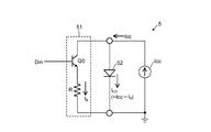
図12は、従来のシャント型LDドライバの構成を示す図である。
送信フロントエンド5において、レーザダイオード52に対して並列にシャント型LDドライバ51を接続し、送信すべき信号Dinに応じてシャント型LDドライバ51のトランジスタQ0を制御することにより、送信すべき信号Dinを光信号に変換して送信することができる。
FIG. 12 is a diagram showing a configuration of a conventional shunt type LD driver.
In the
本願発明者らが、従来のシャント型LDドライバをPAM方式の光通信ネットワークの送信フロントエンドに適用することを検討したところ、従来のシャント型LDドライバでは、トランジスタQ0に電流が流れるときにトランジスタQ0の耐圧低下によってトランジスタQ0が故障するおそれがあることが明らかとなった。以下、詳細に説明する。 The inventors of the present application studied applying the conventional shunt type LD driver to the transmission front end of the PAM optical communication network. In the conventional shunt type LD driver, when current flows through the transistor Q0, the transistor Q0 It has become clear that the transistor Q0 may be damaged due to a decrease in withstand voltage. Details will be described below.
図13は、従来のシャント型LDドライバを構成するトランジスタQ0のコレクタ電流Ic対コレクタ−エミッタ間電圧VCE特性の一例を示す図である。
図14は、シャント型LDドライバによって駆動されるレーザダイオードLD0のI−V特性の一例を示す図である。
FIG. 13 is a diagram showing an example of the collector current Ic vs. collector-emitter voltage V CE characteristics of the transistor Q0 constituting the conventional shunt type LD driver.
FIG. 14 is a diagram illustrating an example of the IV characteristic of the laser diode LD0 driven by the shunt type LD driver.
一般に、バイポーラトランジスタは、ベース・エミッタ間電圧VBE(ベース電流)が大きくなるほど電流Icが増加するが、ブレークダウンボルテージである一次降伏した後も電流Icを更に増加させると、局部的な電流集中が発生し、トランジスタQ0の耐圧が低下する現象(二次降伏現象)が起こることが知られている。
そのため、図12に示すシャント型LDドライバにおいてトランジスタQ0を駆動する際には、図13に示すように、二次降伏現象が発生する境界200の右側の降伏領域202ではなく、左側の安全動作領域201においてトランジスタQ0を動作させる必要がある。
Generally, in a bipolar transistor, the current Ic increases as the base-emitter voltage V BE (base current) increases. However, if the current Ic is further increased after the primary breakdown, which is a breakdown voltage, local current concentration occurs. It is known that a phenomenon (secondary breakdown phenomenon) in which the breakdown voltage of the transistor Q0 is reduced occurs.
Therefore, when driving the transistor Q0 in the shunt type LD driver shown in FIG. 12, as shown in FIG. 13, not the breakdown region 202 on the right side of the
一方、レーザダイオードは、図14に示すように、レーザダイオードの両端の電圧VLDに対してレーザダイオードの電流ILDが急峻に変化するI−V特性を有している。
シャント型LDドライバにおいて、レーザダイオードLD0に流れる電流ILDは、定電流源から出力される電流Iccから、レーザダイオードLD0と並列に接続されたトランジスタQ0によって引き抜かれる電流I0(Ic)の大きさによって決まり、ILD=Icc−I0となる。
On the other hand, as shown in FIG. 14, the laser diode has an IV characteristic in which the current I LD of the laser diode changes sharply with respect to the voltage V LD across the laser diode.
In the shunt type LD driver, the current I LD flowing through the laser diode LD0 is the magnitude of the current I 0 (Ic) drawn from the current Icc output from the constant current source by the transistor Q0 connected in parallel with the laser diode LD0. And I LD = Icc−I 0 .
図15は、レーザダイオードLD0に流れる電流ILDとトランジスタQ0の動作点の関係を示す図である。
図15に示すように、シャント型LDドライバでは、トランジスタQ0のベース・エミッタ間電圧VBEを変化させることにより、レーザダイオードLD0の電流ILDを変化させることができる。
Figure 15 is a diagram showing the relationship of the operating point of the current I LD and the transistor Q 0 flowing through the laser diode LD0.
As shown in FIG. 15, the shunt LD driver, by changing the base-emitter voltage V BE of the transistor Q 0, it is possible to vary the current I LD of the laser diode LD0.
例えば、図15に示すように、ベース・エミッタ間電圧VBEを最大値VBEmaxとした場合、トランジスタQ0のコレクタ・エミッタ間電圧VCEが最小となり、トランジスタQ0のコレクタ電流Icが最大値I0maxとなる。このとき、レーザダイオードLD0の電流ILDは最小となる。一方、トランジスタQ0のベース・エミッタ間電圧VBEを最小値VBEminとした場合、トランジスタQ0のコレクタ・エミッタ間電圧VCEが最大となり、トランジスタQ0のコレクタ電流Icが最小値I0mimとなる。このとき、レーザダイオードLD0の電流ILDは最大となる。 For example, as shown in FIG. 15, when the base-emitter voltage V BE is the maximum value V BEmax , the collector-emitter voltage V CE of the transistor Q0 is minimum, and the collector current Ic of the transistor Q0 is the maximum value I 0max. It becomes. At this time, the current I LD of the laser diode LD0 is minimized. On the other hand, when the base-emitter voltage V BE of the transistor Q0 is set to the minimum value V BEmin , the collector-emitter voltage V CE of the transistor Q0 is maximum, and the collector current Ic of the transistor Q0 is minimum value I 0mim . At this time, the current I LD of the laser diode LD0 is maximized.
このように、トランジスタQ0に流れる電流I0(コレクタ電流Ic)は、レーザダイオードLD0のI−V特性300に沿って変化する。そのため、ベース・エミッタ間電圧を最大値VBEmaxとしてレーザダイオードLD0の電流ILDを最小とする場合に、レーザダイオードLD0のI−V特性が急峻であるほど、トランジスタQ0の動作点が境界200の右側、すなわち降伏領域202に入り、耐圧低下によるトランジスタQ0の破壊が起こるおそれがある。
Thus, the current I 0 (collector current Ic) flowing through the transistor Q0 varies along the IV
本発明は、上記の問題に鑑みてなされたものであり、本発明の目的は、トランジスタの二次降伏による故障を回避しつつ、レーザダイオードを高速に動作させることが可能なドライバを提供することにある。 The present invention has been made in view of the above problems, and an object of the present invention is to provide a driver capable of operating a laser diode at high speed while avoiding a failure due to secondary breakdown of a transistor. It is in.
本発明に係るドライバ(1)は、送信対象の信号(Din)を入力する入力端子(Pin)と、駆動対象のレーザダイオード(LD0)のアノード電極に接続するための出力端子(Pout)と、制御電極が入力端子に接続されたトランジスタ(Q0)と、第1電源電圧が供給される第1電源ライン(GND)とトランジスタの第1主電極との間に接続された第1抵抗(R0)と、出力端子とトランジスタの第2主電極との間に接続された第2抵抗(R1)と、前記第2抵抗と並列に接続された第1容量(C1)と、出力端子に電流を供給する電流供給部(Lc,12)とを有することを特徴とする。 The driver (1) according to the present invention includes an input terminal (Pin) for inputting a transmission target signal (Din), an output terminal (Pout) for connection to an anode electrode of a laser diode (LD0) to be driven, A transistor (Q0) having a control electrode connected to an input terminal, and a first resistor (R0) connected between a first power supply line (GND) to which a first power supply voltage is supplied and a first main electrode of the transistor. And a second resistor (R1) connected between the output terminal and the second main electrode of the transistor, a first capacitor (C1) connected in parallel with the second resistor, and supplying a current to the output terminal And a current supply unit (Lc, 12).
上記ドライバにおいて、電流供給部は、第1電源電圧よりも大きい第2電源電圧が供給される第2電源ライン(VCC)と出力端子との間に接続されたコイル(Lc)を含んでもよい。 In the driver, the current supply unit may include a coil (Lc) connected between a second power supply line (VCC) to which a second power supply voltage higher than the first power supply voltage is supplied and an output terminal.
上記ドライバにおいて、電流供給部は、第1電源電圧よりも大きい第2電源電圧が供給される第2電源ライン(VCC)と出力端子との間に接続された定電流源(12)を含んでもよい。 In the driver, the current supply unit may include a constant current source (12) connected between a second power supply line (VCC) to which a second power supply voltage higher than the first power supply voltage is supplied and an output terminal. Good.
上記ドライバにおいて、入力端子は、第1端子(Pin0)と第2端子(Pin1)を含み、トランジスタ(Q0)と、第1抵抗(R0)と、第2抵抗(R1)と、第1容量(C1)とを一組とする基本駆動回路(10)をN(Nは2以上の整数)個有し、N個の基本駆動回路のうち、M(MはNよりも小さい正の整数)個の基本駆動回路を構成する夫々のトランジスタの制御電極は、第1端子に接続され、N個の基本駆動回路のうち、残りの(N−M)個の基本駆動回路を構成する夫々のトランジスタの制御電極は、第2端子に接続されていてもよい。 In the driver, the input terminal includes a first terminal (Pin0) and a second terminal (Pin1). The transistor (Q0), the first resistor (R0), the second resistor (R1), and the first capacitor ( C (1) and N (N is an integer greater than or equal to 2) basic drive circuits (10), and M (M is a positive integer smaller than N) of the N basic drive circuits. The control electrodes of the respective transistors constituting the basic drive circuit are connected to the first terminal, and among the N basic drive circuits, the remaining (NM) basic drive circuits of the respective transistors constituting the basic drive circuit are connected. The control electrode may be connected to the second terminal.
上記ドライバにおいて、第1バイアス電圧が供給される第1バイアス端子(Va)と、第1バイアス電圧よりも低い第2バイアス電圧が供給される第2バイアス端子(Vb)と、一端が、M個の基本駆動回路を構成する夫々のトランジスタの制御電極に共通に接続され、他端が第1端子に接続された第2容量(Ca)と、第1バイアス端子と第2容量の一端との間に接続された第3抵抗(Ra0)と、第2バイアス端子と第2容量の一端との間に接続された第4抵抗(Rb0)と、一端が(N−M)個の基本駆動回路を構成する夫々のトランジスタの制御電極に共通に接続され、他端が第2端子に接続された第3容量(Cb)と、第1バイアス端子と第3容量の一端との間に接続された第5抵抗(Ra1)と、第2バイアス端子と第3容量の一端との間に接続された第6抵抗(Rb1)とを更に有してもよい。 In the driver, a first bias terminal (Va) to which a first bias voltage is supplied, a second bias terminal (Vb) to which a second bias voltage lower than the first bias voltage is supplied, and M one ends. Between the second capacitor (Ca) connected in common to the control electrode of each of the transistors constituting the basic drive circuit and having the other end connected to the first terminal, and between the first bias terminal and one end of the second capacitor A third resistor (Ra0) connected to the second resistor, a fourth resistor (Rb0) connected between the second bias terminal and one end of the second capacitor, and (NM) basic drive circuits at one end. A third capacitor (Cb) connected in common to the control electrode of each of the transistors, the other end connected to the second terminal, and a first capacitor connected between the first bias terminal and one end of the third capacitor. 5 resistors (Ra1), the second bias terminal and the third capacitor Sixth resistor (Rb1) and may further include a connected between an end.
上記ドライバにおいて、N=3Mであってもよい。 In the driver, N = 3M may be used.
本発明によれば、トランジスタの二次降伏による故障を回避しつつ、レーザダイオードを高速に動作させることが可能となる。 According to the present invention, it is possible to operate a laser diode at high speed while avoiding a failure due to secondary breakdown of a transistor.
以下、本発明の実施の形態について図を参照して説明する。なお、以下の説明において、各実施の形態で共通する構成要素には同一の参照符号を付し、繰り返しの説明を省略する。 Hereinafter, embodiments of the present invention will be described with reference to the drawings. In the following description, the same reference numerals are given to components common to the respective embodiments, and repeated description is omitted.
≪実施の形態1≫
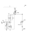
図1は、本発明の一実施の形態に係るLDドライバを備えた光送信器の送信フロントエンドの構成を示す図である。
同図に示される送信フロントエンド100は、送信すべき情報を光ファイバ等から成る光通信ネットワークに対して光信号として出力する光送信器において、上記情報が重畳された電気信号を光信号に変換する機能部である。
<<
FIG. 1 is a diagram illustrating a configuration of a transmission front end of an optical transmitter including an LD driver according to an embodiment of the present invention.
The transmission
図1に示されるように、送信フロントエンド100は、レーザダイオードLD0と、レーザダイオードLD0を駆動するためのLDドライバ1とを備えている。なお、本実施の形態では、電源電圧VCCが供給される信号ラインを“電源ラインVCC”とし、電源電圧VCCよりも小さい電源電圧が供給される信号ラインを“グラウンドラインGND”とする。
As shown in FIG. 1, the transmission
レーザダイオード(半導体レーザ)LD0は、供給された駆動電流ILDに応じた強度の光を出力する発光素子である。レーザダイオードLD0は、直接変調半導体レーザ(DML:Directly Modulated Laser)である。レーザダイオードLD0のアノードは、出力端子Poutに接続され、レーザダイオードLD0のカソードは、グラウンドラインGNDに接続される。レーザダイオードLD0のアノードと出力端子Poutとは、例えば、ボンディングワイヤまたはフリップチップ接続によって接続されている。 A laser diode (semiconductor laser) LD0 is a light-emitting element that outputs light having an intensity corresponding to the supplied drive current I LD. The laser diode LD0 is a direct modulation semiconductor laser (DML: Directly Modulated Laser). The anode of the laser diode LD0 is connected to the output terminal Pout, and the cathode of the laser diode LD0 is connected to the ground line GND. The anode of the laser diode LD0 and the output terminal Pout are connected by, for example, a bonding wire or flip chip connection.
なお、レーザダイオードLD0のアノードと出力端子Poutとの間に接続されるボンディングワイヤまたはフリップチップ接続による配線は、寄生インダクタンスを有している。一般にボンディングワイヤ(金ワイヤ)のインダクタ成分は約1nH/mmであり、フリップチップ接続の場合には、ボンディングワイヤに比べてインダクタ成分が小さくなる傾向がある。 Note that the bonding wire connected between the anode of the laser diode LD0 and the output terminal Pout or the wiring by flip chip connection has a parasitic inductance. Generally, the inductor component of the bonding wire (gold wire) is about 1 nH / mm, and in the case of flip chip connection, the inductor component tends to be smaller than that of the bonding wire.
LDドライバ1は、入力端子Pinに入力された入力信号Dinに基づいて、レーザダイオードLD0の駆動電流ILDを直接変調することにより、レーザダイオードLD0による光出力を変調するDMLドライバである。具体的に、LDドライバ1は、コイルLcと、入力整合部11と、基本駆動回路10とを含む。
The
コイルLcは、レーザダイオードLD0の駆動電流ILDを供給するための素子である。コイルLcは、例えば高周波用チョークコイルである。コイルLcの一端は、電源電圧VCCが供給される電源端子に接続され、コイルLcの他端は、出力端子Poutに接続される。コイルLcは、電源ラインVCCから基本駆動回路10とレーザダイオードLD0とに対してDCバイアスを供給するとともに、高周波動作時に高インピーダンスとなる。以下、コイルLcから出力される電流をIccと表記する。
The coil Lc is an element for supplying a drive current I LD for the laser diode LD0. The coil Lc is, for example, a high frequency choke coil. One end of the coil Lc is connected to a power supply terminal to which the power supply voltage VCC is supplied, and the other end of the coil Lc is connected to the output terminal Pout. The coil Lc supplies a DC bias from the power supply line VCC to the
入力整合部11は、所定の変調方式に従って変調されることにより送信すべき情報が重畳された入力信号Dinを出力する回路(例えば、図11におけるDAC)と、その入力信号Dinを入力する後述のLDドライバ10との間のインピーダンスを整合するための機能部である。
入力整合部11は、一端が入力端子Pinに接続され、他端がグラウンドラインGNDに接続される抵抗Rmを含む。例えば、50Ω系の伝送線路から入力信号Dinを入力する場合、Rm=50Ωである。
The
The
基本駆動回路10は、コイルLcとレーザダイオードLD0とを結ぶ電流経路を分岐させる分流経路を形成し、入力信号Dinに基づいて上記分流経路に流れる電流I0を制御することにより、レーザダイオードLD0の駆動電流ILDを制御するシャント型ドライバ回路を構成している。具体的に、基本駆動回路10は、トランジスタQ0、抵抗R0,R1、および容量C1を含む。
The
トランジスタQ0は、上記分流経路に流れる電流I0を制御するための素子であり、例えばNPN型のバイポーラトランジスタである。トランジスタQ0の制御電極としてのベース電極は入力端子Pinに接続されている。 The transistor Q0 is an element for controlling the current I 0 flowing through the shunt path, and is, for example, an NPN bipolar transistor. A base electrode as a control electrode of the transistor Q0 is connected to the input terminal Pin.
抵抗R0は、グラウンドラインGNDとトランジスタQ0の第1主電極としてのエミッタ電極との間に接続されている。抵抗R1は、出力端子PoutとトランジスタQ0の第2主電極としてのコレクタ電極との間に接続されている。容量C1は、抵抗R1と並列に接続されている。すなわち、容量C1は、出力端子PoutとトランジスタQ0のコレクタ電極との間に接続されている。 The resistor R0 is connected between the ground line GND and the emitter electrode as the first main electrode of the transistor Q0. The resistor R1 is connected between the output terminal Pout and the collector electrode as the second main electrode of the transistor Q0. The capacitor C1 is connected in parallel with the resistor R1. That is, the capacitor C1 is connected between the output terminal Pout and the collector electrode of the transistor Q0.
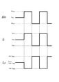
次に、上述の回路構成を有するLDドライバ1の動作について図2、3を用いて説明する。
Next, the operation of the
図2は、実施の形態1に係るLDドライバ1におけるトランジスタQ0の動作点を示す図である。
図2において、参照符号300は、従来のシャント型LDドライバ(図12参照)を用いた場合のレーザダイオードLD0に流れる電流ILDの特性を表し、参照符号300Aは、実施の形態1に係るLDドライバ1を用いた場合のレーザダイオードLD0に流れる電流ILDの特性を表している。
FIG. 2 is a diagram illustrating an operating point of the transistor Q0 in the
In FIG. 2,
図3は、実施の形態1に係るLDドライバ1によってレーザダイオードLD0を駆動したときのタイミングチャート図である。
FIG. 3 is a timing chart when the laser diode LD0 is driven by the
図2,3に示すように、バイアス電圧Vbiasを基準として上下の方向に変化する入力信号DinをLDドライバ1に入力する場合を考える。
先ず、入力端子Pinにバイアス電圧Vbiasのみが印加された状態(AC成分なし)では、コイルLcは低インピーダンス状態(短絡状態)となり、出力端子Poutの電圧は略電源電圧Vccとなる。このとき、トランジスタQ0に流れる電流をI0biasとすると、トランジスタQ0のコレクタ・エミッタ間電圧VCEは、VCEbias=VCC−(R1+R0)I0biasで表される。このとき、レーザダイオードLD0に流れる電流をILDbiasとする。
Consider the case where an input signal Din that changes in the vertical direction with respect to the bias voltage V bias is input to the
First, in a state where only the bias voltage V bias is applied to the input terminal Pin (no AC component), the coil Lc is in a low impedance state (short circuit state), and the voltage at the output terminal Pout is substantially the power supply voltage Vcc. At this time, assuming that the current flowing through the transistor Q0 is I 0bias , the collector-emitter voltage V CE of the transistor Q0 is represented by V CEbias = VCC− (R1 + R0) I 0bias . At this time, the current flowing through the laser diode LD0 is I LDbias .
次に、バイアス電圧Vbiasに重畳したデータ(AC成分)が印加された場合を考える。例えば、入力信号Dinとして、バイアス電圧Vbiasを基準としてハイレベルとなる高周波信号Vinmaxが入力された場合、トランジスタQ0が更にオンする方向に変化する。このとき、コイルLcは、高周波信号に対して高インピーダンスとなり、図3に示すように、トランジスタQ0に流れる電流IOが増加し、レーザダイオードLD0に流れる電流ILDは、ILDbiasから減少する。一方、入力信号Dinとして、バイアス電圧Vbiasを基準としてローレベルとなる高周波信号Vinmin)が入力された場合には、トランジスタQ0がオフする方向に変化する。このとき、コイルLcは高周波信号に対して高インピーダンスとなり、図3に示すように、トランジスタQ0に流れる電流IOが減少し、レーザダイオードLD0に流れる電流ILDは、ILDbiasから増加する。 Next, consider a case where data (AC component) superimposed on the bias voltage V bias is applied. For example, when a high-frequency signal Vin max that is at a high level with reference to the bias voltage V bias is input as the input signal Din, the transistor Q0 is further turned on. At this time, the coil Lc has a high impedance with respect to the high-frequency signal, and as shown in FIG. 3, the current I O flowing through the transistor Q0 increases, and the current I LD flowing through the laser diode LD0 decreases from I LDbias . On the other hand, when the input signal Din is a high-frequency signal Vin min that is at a low level with reference to the bias voltage V bias , the transistor Q0 is turned off. At this time, the coil Lc has a high impedance with respect to the high-frequency signal, and as shown in FIG. 3, the current I O flowing through the transistor Q0 decreases and the current I LD flowing through the laser diode LD0 increases from I LDbias .
ここで、基本駆動回路10におけるトランジスタQ0のコレクタ電極から出力端子Pout側をみたときのインピーダンスZloadは、下記式(1)で表すことができる。
Here, the impedance Z load when the output terminal Pout side is seen from the collector electrode of the transistor Q0 in the

上記式(1)から理解されるように、低周波動作時(ω→0)には、Zload=R1となるので、トランジスタQ1のコレクタ電位は、出力端子Poutの電圧(≒VCC)よりも(R1×I0)だけ低下する。これにより、図2に示すように、レーザダイオードLD0に流れる電流ILDが最小となるとき、すなわちトランジスタQ0のコレクタ電流Icが最大(I0max)となるとき、トランジスタQ0は、二次降伏が発生する降伏領域202ではなく安定動作領域201で動作することが可能となり、トランジスタQ0の破壊を防止することが可能となる。 As understood from the above equation (1), during low frequency operation (ω → 0), Z load = R1, so that the collector potential of the transistor Q1 is higher than the voltage of the output terminal Pout (≈VCC). Decrease by (R1 × I 0 ). As a result, as shown in FIG. 2, when the current I LD flowing through the laser diode LD0 becomes the minimum, that is, when the collector current Ic of the transistor Q0 becomes the maximum (I 0max ), the transistor Q0 generates the secondary breakdown. Therefore, it is possible to operate in the stable operation region 201 instead of the breakdown region 202, and it is possible to prevent the transistor Q0 from being broken.
一方、高周波動作時(ω→∞)には、抵抗R1に並列に接続された容量C1により、インピーダンスZloadが小さくなるため、R1のみをトランジスタQ0に直列に接続する場合に比べて、高周波数領域におけるLDドライバ1の帯域の劣化を補償することができる。
On the other hand, during high frequency operation (ω → ∞), the impedance Z load is reduced by the capacitor C1 connected in parallel to the resistor R1, so that the frequency is higher than when only R1 is connected in series to the transistor Q0. The degradation of the band of the
以上、実施の形態1に係るLDドライバ1によれば、シャント型LDドライバのトランジスタQ0と出力端子Poutとの間に抵抗R1を直列に接続するとともに、抵抗R1と並列に容量C1を接続することにより、低周波動作時には、トランジスタQ1のコレクタ電極に印加される電圧を小さくしてトランジスタの二次降伏による故障を回避しつつ、高周波動作時には、インピーダンスZloadを小さくしてLDドライバ1の帯域の劣化を補償することにより、レーザダイオードを高速に動作させることが可能となる。
As described above, according to the
また、レーザダイオードLD0とLDドライバ1に電流を供給する電流供給部としてコイルLc(チョークコイル)を用いているので、カレントミラー回路等から成る定電流源を用いる場合に比べて、より低消費電力となる。
In addition, since the coil Lc (choke coil) is used as a current supply unit that supplies current to the laser diode LD0 and the
≪実施の形態2≫
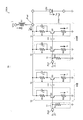
図4は、実施の形態2に係るLDドライバを備えた光送信器の送信フロントエンドの構成を示す図である。
同図に示される送信フロントエンド100Aは、PAM方式に対応した光送信器の送信フロントエンドであり、PAM4信号を生成するLDドライバ1Aを有する。
<< Embodiment 2 >>
FIG. 4 is a diagram illustrating a configuration of a transmission front end of the optical transmitter including the LD driver according to the second embodiment.
The transmission
LDドライバ1Aは、出力端子PoutとグラウンドノードGNDとの間に共通に接続されるN(Nは2以上の整数)個の基本駆動回路10と、2つの入力端子Pin0,Pin1と、入力端子Pin0,Pin1に夫々接続される2つの入力整合部11と、コイルLcとを含む。
The
N=3M(MはNよりも小さい正の整数)としたとき、N個の基本駆動回路10のうち、M個の基本駆動回路10を構成する夫々のトランジスタQ0のベース電極は、入力端子Pin0に接続されている。
When N = 3M (M is a positive integer smaller than N), among the N
一方、N個の基本駆動回路10のうち、(N−M)個、すなわち2M個の基本駆動回路10を構成する夫々のトランジスタQ0のベース電極は、入力端子Pin1に接続されている。
On the other hand, among the N
ドライバ1Aには、2ビットの入力信号D0,D1が入力される。具体的には、LSBとしての入力信号D0が、M個の基本駆動回路10が接続されている入力端子Pin0に入力され、MSBとしての入力信号D1が2M個の基本駆動回路10が接続された入力端子Pin1に入力される。
2-bit input signals D0 and D1 are input to the
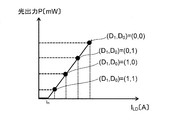
図5は、2ビットの入力信号D0,D1をドライバ1Aに入力したときのレーザダイオードLD0に流れる電流ILDのアイ波形の一例を示す図である。図6は、2ビットの入力信号D0,D1をドライバ1Aに入力したときの光送信器の光出力の一例を示す図である。
図5,6では、I0min=0としている。また、以下の説明では、入力信号D0,D1の信号レベルがトランジスタQ0の閾値電圧よりも高い場合を“1”、入力信号D0,D1の信号レベルがトランジスタQ0の閾値電圧よりも低い場合を“0”と表記する。
FIG. 5 is a diagram illustrating an example of an eye waveform of the current I LD that flows through the laser diode LD0 when the 2-bit input signals D0 and D1 are input to the
5 and 6, I 0min = 0. Further, in the following description, “1” is used when the signal level of the input signals D0 and D1 is higher than the threshold voltage of the transistor Q0, and “when the signal level of the input signals D0 and D1 is lower than the threshold voltage of the transistor Q0”. Indicated as 0 ”.
図5に示すように、入力信号(D1,D0)=(0,0)の場合、M個の基本駆動回路10と2M個の基本駆動回路10の夫々に流れる電流I0は、“I0=I0min=0”となり、レーザダイオードLD0に流れる電流ILDは、“ILD=Icc”となる。
As shown in FIG. 5, when the input signal (D1, D0) = (0, 0), the current I 0 flowing through each of the M
また、入力信号(D1,D0)=(0,1)の場合、M個の基本駆動回路10の夫々に流れる電流I0は“I0max”となり、2M個の基本駆動回路10の夫々に流れる電流I0は“0”となるため、レーザダイオードLD0に流れる電流ILDは、“ILD=Icc−M×I0max”となる。
When the input signal (D1, D0) = (0, 1), the current I 0 flowing through each of the M
また、入力信号(D1,D0)=(1,0)の場合、M個の基本駆動回路10の夫々に流れる電流I0は“0”となり、2M個の基本駆動回路10の夫々に流れる電流I0は“I0max”となるため、レーザダイオードLD0に流れる電流ILDは、“ILD=ICC−2M×I0max”となる。
When the input signal (D1, D0) = (1, 0), the current I 0 flowing through each of the M
更に、入力信号(D1,D0)=(1,1)の場合、M個の基本駆動回路10と2M個の基本駆動回路10の夫々に流れる電流I0は、“I0=I0max”となり、レーザダイオードLD0に流れる電流ILDは、“ILD=Icc−3M×I0max”となる。
Further, when the input signals (D1, D0) = (1, 1), the currents I 0 flowing through the M
以上のように、入力信号D0,D1の論理の組合せに応じてレーザダイオードLD0に流れる電流ILDが図5に示すように変化するので、図4に示す送信フロントエンド100Aを有する光送信器から、図6に示すような電流ILDのPAM4波形に対応する4値の光出力を得ることができる。
As described above, the current I LD flowing through the laser diode LD0 changes as shown in FIG. 5 in accordance with the logic combination of the input signals D0 and D1, so that the optical transmitter having the transmission
以上、実施の形態2に係るLDドライバ1Aによれば、実施の形態1に係るLDドライバ1と同様に、PAM4に対応した光送信器においてトランジスタの二次降伏による故障を回避しつつ、レーザダイオードを高速に動作させることが可能となる。
As described above, according to the
≪実施の形態3≫
図7は、実施の形態3に係るLDドライバを備えた光送信器の送信フロントエンドの構成を示す図である。
同図に示される送信フロントエンド100BにおけるLDドライバ1Bは、実施の形態2に係るPAM4方式のLDドライバ1Aと入力整合部の回路構成が相違し、その他の点は実施の形態2に係るLDドライバ1Aと同様である。
<< Embodiment 3 >>
FIG. 7 is a diagram illustrating a configuration of a transmission front end of an optical transmitter including an LD driver according to the third embodiment.
The
具体的に、LDドライバ1Bは、抵抗Ra0,Rb0および容量Caから成る入力整合部11Aと、抵抗Ra1,Rb1および容量Cbから成る入力整合部11Bと有する。なお、本実施の形態では、バイアス電圧Vaが供給される信号ラインを“バイアスラインVa”とし、バイアス電圧Vaよりも小さいバイアス電圧Vbが供給される信号ラインを“バイアスラインVb”とする。
Specifically, the
入力端子Pin0側の入力整合部11Aにおいて、バイアスラインVaとバイアスラインVbとの間に抵抗Ra0と抵抗Rb0が直列に接続され、M個の基本駆動回路10における各トランジスタQ0のベース電極、抵抗Ra0、および抵抗Rb0が接続されるノードnaと入力端子Pin0との間に容量Caが接続されている。
In the
入力端子Pin1側の入力整合部11Bは、入力端子Pin0側の入力整合部11Aと同様の回路構成を有する。すなわち、バイアスラインVaとバイアスラインVbとの間に抵抗Ra1と抵抗Rb1が直列に接続され、2M個の基本駆動回路10における各トランジスタQ0のベース電極、抵抗Ra1、および抵抗Rb1が接続されるノードnbと入力端子Pin1との間に容量Cbが接続されている。
The
入力整合部11Aによれば、入力端子Pinから入力された入力信号Dinの直流成分を容量Caによって除去して入力信号Dinの交流成分(RF信号)のみをトランジスタQ0に印加するとともに、トランジスタQ0に任意の入力バイアス電圧を低消費電力で印加することが可能となる。以下、具体例を用いて説明する。
According to the
例えば、50Ω系の伝送線路から入力信号Dinを入力する場合、入力整合部11Aにおける抵抗Ra0と抵抗Rb0との関係は、下記式(2)によって表すことができる。
For example, when the input signal Din is input from a 50Ω transmission line, the relationship between the resistor Ra0 and the resistor Rb0 in the
ここで、トランジスタQ0の入力バイアス電圧として1.0Vを印加するためには、例えば、Vb=0V、Ra0=56Ω、Rb0=467Ω、およびVa=1.12Vとすればよい。このとき、入力整合部11Aの消費電力は約2.4mWとなる。
Here, in order to apply 1.0 V as the input bias voltage of the transistor Q0, for example, Vb = 0V, Ra0 = 56Ω, Rb0 = 467Ω, and Va = 1.12V. At this time, the power consumption of the
これに対して、例えば、実施の形態1に示した抵抗Rm(=50Ω)のみから成る入力整合部11を用いた場合には、トランジスタQ0の入力バイアス電圧が1.0Vのとき、入力整合部11の消費電力は20mWとなり、入力整合部11Aよりも消費電力が大きくなる。
On the other hand, for example, when the
このように、入力整合部11Aを用いることにより、消費電力を抑えつつ、トランジスタQ0の入力バイアス電圧を任意に変更することが可能となる。なお、入力整合部11Bについても同様の効果が期待できる。
Thus, by using the
以上、実施の形態3に係るLDドライバ1Bによれば、実施の形態1に係るLDドライバ1と同様に、PAM4に対応した光送信器においてトランジスタの二次降伏による故障を回避しつつ、レーザダイオードを高速に動作させることが可能となるとともに、より低消費電力で、トランジスタQ0の入力バイアス電圧を任意に変更することが可能となる。
As described above, according to the
なお、図7に示すLDドライバの入力端子Pin0と入力端子Pin1とを結合することにより、NRZ方式のような2値の入力に対応したLDドライバを実現することができる。例えば、図8に示す送信フロントエンド100CのLDドライバ1Cのように、抵抗Ra0,Rb0から成る2組の入力整合部11Cと1つの入力端子Pinとを容量Cinを介して接続する。
It should be noted that by combining the input terminal Pin0 and the input terminal Pin1 of the LD driver shown in FIG. 7, an LD driver corresponding to binary input as in the NRZ method can be realized. For example, like the
これによれば、NRZ方式のような2値入力のLDドライバにおいて、トランジスタの二次降伏による故障を回避しつつ、レーザダイオードを高速に動作させることが可能となるとともに、低消費電力で、トランジスタQ0の入力バイアス電圧を任意に変更することが可能となる。 According to this, in a binary input LD driver such as the NRZ method, it is possible to operate the laser diode at high speed while avoiding a failure due to the secondary breakdown of the transistor, and with low power consumption, the transistor It is possible to arbitrarily change the input bias voltage of Q0.
また、LDドライバ1Cにおいて、2つの入力整合部11Cの何れか一方をノードn0から切り離す(開放)することにより、50Ω系の伝送線路から入力信号Dinを入力する場合に、整合を取ることが容易となる。
Also, in the
≪実施の形態4≫
図9は、実施の形態4に係るLDドライバを備えた光送信器の送信フロントエンドの構成を示す図である。
同図に示されるPAM4方式の送信フロントエンド100DにおけるLDドライバ1Dは、コイルLcの代わりに定電流源Iccを備える点において、実施の形態2に係るLDドライバ1Aと相違し、その他の点は実施の形態2に係るLDドライバ1Aと同様である。
<< Embodiment 4 >>
FIG. 9 is a diagram illustrating a configuration of a transmission front end of an optical transmitter including an LD driver according to the fourth embodiment.
The
具体的には、図9に示すように、LDドライバ1Dは、電源ラインVCCと出力端子Poutとの間に接続された、出力端子Poutに向かって定電流Iccを供給する定電流源12を、コイルLcの代わりに備える。
Specifically, as shown in FIG. 9, the
これによれば、実施の形態1に係るLDドライバ1と同様に、PAM4に対応した光送信器においてトランジスタの二次降伏による故障を回避しつつ、レーザダイオードを高速に動作させることが可能となる。
According to this, similarly to the
以上、本発明者らによってなされた発明を実施の形態に基づいて具体的に説明したが、本発明はそれに限定されるものではなく、その要旨を逸脱しない範囲において種々変更可能であることは言うまでもない。 Although the invention made by the present inventors has been specifically described based on the embodiments, it is needless to say that the present invention is not limited thereto and can be variously modified without departing from the gist thereof. Yes.
例えば、実施の形態2等において、本発明に係るLDドライバをPAM4方式の光送信器に適用する場合を例示したが、これに限られず、例えば8値等のPAM方式に対応した光送信器のLDドライバとして適用することも可能である。この場合には、入力端子と入力端子に接続する基本駆動回路を必要な数だけ追加すればよい。 For example, in the second embodiment and the like, a case where the LD driver according to the present invention is applied to a PAM4 optical transmitter is illustrated. However, the present invention is not limited to this, and for example, an optical transmitter compatible with a PAM system such as 8-level It can also be applied as an LD driver. In this case, a necessary number of basic drive circuits connected to the input terminal and the input terminal may be added.
また、実施の形態2等において、N=3Mである場合を例示したが、N,Mは2以上の任意の整数であればよく、上記の例に限定されるものではない。 In the second embodiment and the like, the case where N = 3M is exemplified, but N and M may be any integers of 2 or more, and are not limited to the above example.
また、実施の形態4において、実施の形態2に係るLDドライバ1AのコイルLcを定電流源12に置き換える場合を例示したが、実施の形態1,3,または4に係るLDドライバ1B,1Cにおいても同様に、コイルLcを定電流源12に置き換えてもよい。
Further, in the fourth embodiment, the case where the coil Lc of the
100,100A,100B,100C,100D…送信フロントエンド、1,1A,1B,1C,1D…LDドライバ、10…基本駆動回路、11,11A,11B,11C,11D…入力整合部、Lc…コイル,12…定電流源、Pin,Pin0,Pin1…入力端子、Pout…出力端子、LD0…レーザダイオード、R0,R1,Rm,Ra0,Ra1,Rb0,Rb1…抵抗、C1,Ca,Cb,Cin…容量、Din,D0,D1…入力信号。 100, 100A, 100B, 100C, 100D ... transmission front end, 1, 1A, 1B, 1C, 1D ... LD driver, 10 ... basic drive circuit, 11, 11A, 11B, 11C, 11D ... input matching unit, Lc ... coil , 12 ... constant current source, Pin, Pin0, Pin1 ... input terminal, Pout ... output terminal, LD0 ... laser diode, R0, R1, Rm, Ra0, Ra1, Rb0, Rb1 ... resistance, C1, Ca, Cb, Cin ... Capacitance, Din, D0, D1... Input signal.
Claims (6)
駆動対象のレーザダイオードのアノード電極に接続するための出力端子と、
制御電極が前記入力端子に接続されたトランジスタと、
第1電源電圧が供給される第1電源ラインと前記トランジスタの第1主電極との間に接続された第1抵抗と、
前記出力端子と前記トランジスタの第2主電極との間に接続された第2抵抗と、
前記第2抵抗と並列に接続された第1容量と、
前記出力端子に電流を供給する電流供給部と、を有する
ドライバ。 An input terminal for inputting a signal to be transmitted;
An output terminal for connection to the anode electrode of the laser diode to be driven;
A transistor having a control electrode connected to the input terminal;
A first resistor connected between a first power supply line to which a first power supply voltage is supplied and a first main electrode of the transistor;
A second resistor connected between the output terminal and the second main electrode of the transistor;
A first capacitor connected in parallel with the second resistor;
A driver for supplying a current to the output terminal;
前記電流供給部は、
前記第1電源電圧よりも大きい第2電源電圧が供給される第2電源ラインと前記出力端子との間に接続されたコイルを含む
ことを特徴とするドライバ。 The driver according to claim 1,
The current supply unit is
A driver comprising a coil connected between a second power supply line to which a second power supply voltage higher than the first power supply voltage is supplied and the output terminal.
前記電流供給部は、
前記第1電源電圧よりも大きい第2電源電圧が供給される第2電源ラインと前記出力端子との間に接続された定電流源を含む
ことを特徴とするドライバ。 The driver according to claim 1,
The current supply unit is
A driver comprising: a constant current source connected between a second power supply line to which a second power supply voltage higher than the first power supply voltage is supplied and the output terminal.
前記入力端子は、第1端子と第2端子を含み、
前記トランジスタと、前記第1抵抗と、前記第2抵抗と、前記第1容量とを一組とする基本駆動回路をN(Nは2以上の整数)個有し、
前記N個の前記基本駆動回路のうち、M(MはNよりも小さい正の整数)個の前記基本駆動回路を構成する夫々の前記トランジスタの前記制御電極は、前記第1端子に接続され、
前記N個の前記基本駆動回路のうち、残りの(N−M)個の前記基本駆動回路を構成する夫々の前記トランジスタの前記制御電極は、前記第2端子に接続されている
ことを特徴とするドライバ。 The driver according to any one of claims 1 to 3,
The input terminal includes a first terminal and a second terminal,
N (N is an integer of 2 or more) basic drive circuits each including the transistor, the first resistor, the second resistor, and the first capacitor,
Among the N basic drive circuits, the control electrodes of the transistors constituting the M (M is a positive integer smaller than N) basic drive circuits are connected to the first terminal,
Of the N basic drive circuits, the control electrodes of the transistors constituting the remaining (N−M) basic drive circuits are connected to the second terminal. To driver.
第1バイアス電圧が供給される第1バイアスラインと、
前記第1バイアス電圧よりも低い第2バイアス電圧が供給される第2バイアスラインと、
一端が、前記M個の前記基本駆動回路を構成する夫々の前記トランジスタの前記制御電極に共通に接続され、他端が前記第1端子に接続された第2容量と、
前記第1バイアスラインと前記第2容量の前記一端との間に接続された第3抵抗と、
前記第2バイアスラインと前記第2容量の前記一端との間に接続された第4抵抗と、
一端が、前記(N−M)個の前記基本駆動回路を構成する夫々の前記トランジスタの前記制御電極に共通に接続され、他端が前記第2端子に接続された第3容量と、
前記第1バイアスラインと前記第3容量の前記一端との間に接続された第5抵抗と、
前記第2バイアスラインと前記第3容量の前記一端との間に接続された第6抵抗と、を更に有する
ことを特徴とするドライバ。 The driver according to claim 4, wherein
A first bias line to which a first bias voltage is supplied;
A second bias line to which a second bias voltage lower than the first bias voltage is supplied;
A second capacitor having one end connected in common to the control electrode of each of the transistors constituting the M basic drive circuits and the other end connected to the first terminal;
A third resistor connected between the first bias line and the one end of the second capacitor;
A fourth resistor connected between the second bias line and the one end of the second capacitor;
A third capacitor having one end connected in common to the control electrode of each of the transistors constituting the (N−M) basic drive circuits, and the other end connected to the second terminal;
A fifth resistor connected between the first bias line and the one end of the third capacitor;
And a sixth resistor connected between the second bias line and the one end of the third capacitor.
N=3M
である
ことを特徴とするドライバ。 The driver according to claim 4 or 5,
N = 3M
The driver characterized by being.
Priority Applications (1)
| Application Number | Priority Date | Filing Date | Title |
|---|---|---|---|
| JP2016078796A JP2017191812A (en) | 2016-04-11 | 2016-04-11 | driver |
Applications Claiming Priority (1)
| Application Number | Priority Date | Filing Date | Title |
|---|---|---|---|
| JP2016078796A JP2017191812A (en) | 2016-04-11 | 2016-04-11 | driver |
Publications (1)
| Publication Number | Publication Date |
|---|---|
| JP2017191812A true JP2017191812A (en) | 2017-10-19 |
Family
ID=60085399
Family Applications (1)
| Application Number | Title | Priority Date | Filing Date |
|---|---|---|---|
| JP2016078796A Pending JP2017191812A (en) | 2016-04-11 | 2016-04-11 | driver |
Country Status (1)
| Country | Link |
|---|---|
| JP (1) | JP2017191812A (en) |
Cited By (1)
| Publication number | Priority date | Publication date | Assignee | Title |
|---|---|---|---|---|
| WO2020195886A1 (en) * | 2019-03-26 | 2020-10-01 | 日本電信電話株式会社 | Dml driver |
Citations (9)
| Publication number | Priority date | Publication date | Assignee | Title |
|---|---|---|---|---|
| JPS6188579A (en) * | 1984-10-08 | 1986-05-06 | Nec Corp | Driving circuit for laser diode |
| JPH01149071A (en) * | 1987-12-07 | 1989-06-12 | Ricoh Co Ltd | Semiconductor laser control device |
| US5398008A (en) * | 1992-08-17 | 1995-03-14 | Alcatel N.V. | Circuit arrangement for amplitude-modulating the drive signal of a laser |
| JP2002111117A (en) * | 2000-09-29 | 2002-04-12 | Brother Ind Ltd | Optical scanner and image forming device equipped with the same |
| JP2004241505A (en) * | 2003-02-04 | 2004-08-26 | Ntt Electornics Corp | E/o conversion circuit |
| JP2007234901A (en) * | 2006-03-01 | 2007-09-13 | Sumitomo Electric Ind Ltd | Semiconductor laser driving circuit |
| JP2009295681A (en) * | 2008-06-03 | 2009-12-17 | Sumitomo Electric Ind Ltd | Laser diode driving circuit |
| JP2013153087A (en) * | 2012-01-25 | 2013-08-08 | Fujikura Ltd | Dc coupling type laser drive circuit and driving method for semiconductor laser element |
| JP2016005193A (en) * | 2014-06-18 | 2016-01-12 | 日本電信電話株式会社 | Optical access system, terminator, home device and optical access method |
-
2016
- 2016-04-11 JP JP2016078796A patent/JP2017191812A/en active Pending
Patent Citations (9)
| Publication number | Priority date | Publication date | Assignee | Title |
|---|---|---|---|---|
| JPS6188579A (en) * | 1984-10-08 | 1986-05-06 | Nec Corp | Driving circuit for laser diode |
| JPH01149071A (en) * | 1987-12-07 | 1989-06-12 | Ricoh Co Ltd | Semiconductor laser control device |
| US5398008A (en) * | 1992-08-17 | 1995-03-14 | Alcatel N.V. | Circuit arrangement for amplitude-modulating the drive signal of a laser |
| JP2002111117A (en) * | 2000-09-29 | 2002-04-12 | Brother Ind Ltd | Optical scanner and image forming device equipped with the same |
| JP2004241505A (en) * | 2003-02-04 | 2004-08-26 | Ntt Electornics Corp | E/o conversion circuit |
| JP2007234901A (en) * | 2006-03-01 | 2007-09-13 | Sumitomo Electric Ind Ltd | Semiconductor laser driving circuit |
| JP2009295681A (en) * | 2008-06-03 | 2009-12-17 | Sumitomo Electric Ind Ltd | Laser diode driving circuit |
| JP2013153087A (en) * | 2012-01-25 | 2013-08-08 | Fujikura Ltd | Dc coupling type laser drive circuit and driving method for semiconductor laser element |
| JP2016005193A (en) * | 2014-06-18 | 2016-01-12 | 日本電信電話株式会社 | Optical access system, terminator, home device and optical access method |
Cited By (3)
| Publication number | Priority date | Publication date | Assignee | Title |
|---|---|---|---|---|
| WO2020195886A1 (en) * | 2019-03-26 | 2020-10-01 | 日本電信電話株式会社 | Dml driver |
| JP2020161594A (en) * | 2019-03-26 | 2020-10-01 | 日本電信電話株式会社 | DML driver |
| JP7215282B2 (en) | 2019-03-26 | 2023-01-31 | 日本電信電話株式会社 | DML driver |
Similar Documents
| Publication | Publication Date | Title |
|---|---|---|
| JP5337886B2 (en) | DC coupled laser driving circuit and semiconductor laser element driving method | |
| Webster et al. | Low-power MOS-capacitor based silicon photonic modulators and CMOS drivers | |
| US10637207B2 (en) | Directly modulated laser drive circuit | |
| US6242870B1 (en) | Light emitting device driving circuit | |
| US6778571B2 (en) | Laser driver circuit | |
| WO2019181362A1 (en) | Dml driver | |
| US20130121356A1 (en) | Driver circuit and optical transmitter | |
| JP2013020173A (en) | Driving circuit of external modulation type laser element | |
| CN109156070A (en) | Driving device | |
| TW200822586A (en) | Asymmetric rise/fall time and duty cycle control circuit | |
| CN102637996A (en) | Symmetrical, direct coupled laser drivers | |
| CN105717590B (en) | Improve the device and application process of SFP optical module optical modulation amplitudes | |
| JP2017191812A (en) | driver | |
| JP2020161594A (en) | DML driver | |
| JP6849515B2 (en) | DML driver | |
| US7680164B1 (en) | Configurable laser driver with common anode and common cathode outputs | |
| US7684452B1 (en) | Enhancing the transition rate of a laser | |
| US10630052B2 (en) | Efficiency improved driver for laser diode in optical communication | |
| CN113540968A (en) | Structure of sinking type direct modulation laser and driver and application thereof | |
| JP2010129570A (en) | Laser driving circuit | |
| JP2016122898A (en) | Dml driver and transmission front end | |
| JP2004241505A (en) | E/o conversion circuit | |
| JP2008034479A (en) | Laser diode drive circuit | |
| CN111819742B (en) | Laser diode driver with improved efficiency in optical communications | |
| US8803490B2 (en) | Current-mode active termination |
Legal Events
| Date | Code | Title | Description |
|---|---|---|---|
| A621 | Written request for application examination |
Free format text: JAPANESE INTERMEDIATE CODE: A621 Effective date: 20180702 |
|
| A977 | Report on retrieval |
Free format text: JAPANESE INTERMEDIATE CODE: A971007 Effective date: 20190530 |
|
| A131 | Notification of reasons for refusal |
Free format text: JAPANESE INTERMEDIATE CODE: A131 Effective date: 20190625 |
|
| A02 | Decision of refusal |
Free format text: JAPANESE INTERMEDIATE CODE: A02 Effective date: 20200107 |