JP2017191007A - Demodulator - Google Patents
Demodulator Download PDFInfo
- Publication number
- JP2017191007A JP2017191007A JP2016080570A JP2016080570A JP2017191007A JP 2017191007 A JP2017191007 A JP 2017191007A JP 2016080570 A JP2016080570 A JP 2016080570A JP 2016080570 A JP2016080570 A JP 2016080570A JP 2017191007 A JP2017191007 A JP 2017191007A
- Authority
- JP
- Japan
- Prior art keywords
- value
- signal
- detection
- carrier wave
- combined
- Prior art date
- Legal status (The legal status is an assumption and is not a legal conclusion. Google has not performed a legal analysis and makes no representation as to the accuracy of the status listed.)
- Granted
Links
Images





Landscapes
- Gyroscopes (AREA)
Abstract
【課題】より正確にベース信号を復調できる、ジャイロセンサ装置の復調装置を提供する。
【解決手段】センサ回路部は、搬送波に同期した半周期である前半の半周期において合成信号を積分した値と前半の半周期に続く後半の半周期において合成信号を積分した値との差を表す検波値と、合成信号を1周期分積分した値を表すバイアス値と、の相関関係に応じて予め設定された、バイアス値を検波相当値に変換するための補正値を取得するS150。ベース信号が合成信号に合成されていないときにおいて、バイアス値を取得しS120、バイアス値と補正値とに基づいて検波相当値を演算し、基準値として保持するS160。ベース信号が合成信号に合成されているときにおいて、検波値を取得しS220、検波値と基準値との差異に基づいてベース信号を抽出するS230。
【選択図】図6A gyro sensor device demodulator capable of demodulating a base signal more accurately is provided.
A sensor circuit unit calculates a difference between a value obtained by integrating a synthesized signal in a first half cycle that is a half cycle synchronized with a carrier wave and a value obtained by integrating a synthesized signal in a second half cycle following the first half cycle. A correction value for converting the bias value into a detection equivalent value, which is set in advance according to the correlation between the detection value to be expressed and the bias value representing the value obtained by integrating the combined signal for one period, is obtained (S150). When the base signal is not combined with the combined signal, a bias value is acquired and S120 is calculated, a detection equivalent value is calculated based on the bias value and the correction value, and held as a reference value S160. When the base signal is combined with the combined signal, a detection value is acquired (S220), and a base signal is extracted based on the difference between the detection value and the reference value (S230).
[Selection] Figure 6
Description
本発明は、搬送波と、ベース信号が変調された変調信号とが合成された合成信号から、ベース信号を復調する復調装置に関する。 The present invention relates to a demodulator that demodulates a base signal from a synthesized signal obtained by synthesizing a carrier wave and a modulated signal obtained by modulating a base signal.
特許文献1には、ジャイロセンサのエレメントを自励共振回路から出力される信号を用いて振動させ、この信号を搬送波とし、搬送波に対して角速度に応じた信号であるベース信号が変調された変調信号が合成された合成信号から、同期検波を用いてベース信号を抽出する技術が開示されている。
In
しかしながら、上記の技術では、合成信号の波形の中心値(いわゆる0点)となる基準値が温度等の外的要因の影響を受けて変動するので、正確なベース信号を復調できなくなるおそれがあった。 However, in the above technique, the reference value that is the central value (so-called zero point) of the waveform of the synthesized signal fluctuates due to the influence of external factors such as temperature, so there is a risk that an accurate base signal cannot be demodulated. It was.
そこで、このような問題点を鑑み、合成信号からベース信号を復調する復調装置において、より正確にベース信号を復調できるようにすることを本発明の目的とする。 Therefore, in view of such problems, it is an object of the present invention to make it possible to demodulate a base signal more accurately in a demodulator that demodulates a base signal from a synthesized signal.
本発明の復調装置においては、補正値取得部(S150)と、バイアス値取得部(S120)と、基準値保持部(S160)と、検波取得部(S220)と、信号抽出部(S230)と、を備える。 In the demodulator of the present invention, the correction value acquisition unit (S150), the bias value acquisition unit (S120), the reference value holding unit (S160), the detection acquisition unit (S220), and the signal extraction unit (S230) .
補正値取得部は、搬送波に同期した半周期である前半の半周期において合成信号を積分した値と前半の半周期に続く後半の半周期において合成信号を積分した値との差を表す検波値と、合成信号を1周期分積分した値を表すバイアス値と、の相関関係に応じて予め設定された補正値であって、バイアス値を検波値に相当する値を表す検波相当値に変換するための補正値を取得するように構成される。 The correction value acquisition unit detects a difference between a value obtained by integrating the synthesized signal in the first half cycle, which is a half cycle synchronized with the carrier wave, and a value obtained by integrating the synthesized signal in the second half cycle following the first half cycle. And a bias value that represents a value obtained by integrating the synthesized signal for one period, and a correction value that is set in advance according to the correlation, and the bias value is converted into a detection equivalent value that represents a value corresponding to the detection value. Configured to obtain a correction value.
バイアス値取得部は、ベース信号が合成信号に合成されていないときにおいて、バイアス値を取得するように構成される。基準値保持部は、バイアス値と補正値とに基づいて検波相当値を演算し、該検波相当値を基準値として保持するように構成される。検波取得部は、ベース信号が合成信号に合成されているときにおいて、検波値を取得するように構成される。信号抽出部は、検波値と基準値との差異に基づいてベース信号を抽出するように構成される。 The bias value acquisition unit is configured to acquire a bias value when the base signal is not combined with the combined signal. The reference value holding unit is configured to calculate a detection equivalent value based on the bias value and the correction value and hold the detection equivalent value as a reference value. The detection acquisition unit is configured to acquire a detection value when the base signal is combined with the combined signal. The signal extraction unit is configured to extract a base signal based on a difference between the detected value and the reference value.
ここで、本発明においてバイアス値から基準値となる検波相当値を求めるのは、バイアス値が温度等の外的要因によらず、検波値との相関関係が認められたからである。
このような復調装置によれば、バイアス値から得られる検波相当値を搬送波における基準値として設定するので、合成信号からベース信号を復調する復調装置において、外的要因によらず、より正確にベース信号を復調することができる。
Here, the reason why the detection equivalent value serving as the reference value is obtained from the bias value in the present invention is because the correlation between the bias value and the detected value is recognized regardless of external factors such as temperature.
According to such a demodulator, the detection equivalent value obtained from the bias value is set as the reference value in the carrier wave. Therefore, in the demodulator that demodulates the base signal from the synthesized signal, the base signal is more accurately determined regardless of external factors. The signal can be demodulated.
なお、この欄および特許請求の範囲に記載した括弧内の符号は、一つの態様として後述する実施形態に記載の具体的手段との対応関係を示すものであって、本発明の技術的範囲を限定するものではない。 Note that the reference numerals in parentheses described in this column and in the claims indicate the correspondence with the specific means described in the embodiment described later as one aspect, and the technical scope of the present invention. It is not limited.
[1.第1実施形態]
[1−1.構成]
以下、本発明の実施形態を図面に基づいて説明する。ジャイロセンサ装置1は、例えば乗用車等の車両において搭載されている。図1に示すジャイロセンサ装置1は、エレメント10と、センサ回路部20とを備えている。センサ回路部20は、自励共振駆動回路30と、デジタル同期検波回路40、デジタル補正回路50、EPROM60を備えている。センサ回路部20が復調装置に相当する。
[1. First Embodiment]
[1-1. Constitution]
Hereinafter, embodiments of the present invention will be described with reference to the drawings. The
[1−1−1.エレメントの構成]
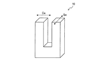
エレメント10には、自励共振駆動回路30から駆動信号Sdrが入力される。このエレメント10は、ここでは図2に示す公知のMEMS音叉型エレメントであるとする。エレメント10は、駆動信号Sdrが入力されることにより、駆動信号Sdrが示す周波数で振動する。駆動信号Sdrによる振動を、以下、駆動振動とし、駆動振動を表す波を搬送波Cwとする。
[1-1-1. Element configuration]
A drive signal Sdr is input to the
このエレメント10に回転方向の外力が加えられると、図2に示すように、エレメント10は、搬送波Cwに対して(すなわち駆動振動に対して)、直交する方向にも振動する。この振動は、エレメント10に加えられる外力Swが、駆動振動により変調された信号であるので、以下、センサ変調信号Smとする。センサ変調信号Smは、搬送波Cwに対して位相が90度ずれた信号である。
When an external force in the rotational direction is applied to the
エレメント10からは、搬送波Cwに対応する自励共振のモニタ信号(以下、モニタ信号という。)と、搬送波Cwにセンサ変調信号Smが重畳した信号である合成信号CSwとが出力される。なお、エレメント10から出力されるモニタ信号および合成信号CSwはアナログ信号である。また、モニタ信号は、センサ変調信号Smを含んでいてもよい。
The
[1−1−2.自励共振系の構成]
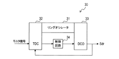
自励共振駆動回路30にはモニタ信号が入力され、この信号に基づいて駆動信号Sdrを生成する。本実施形態の自励共振駆動回路30には、特許文献1に開示されている自励共振回路と同じものを用いることができる。すなわち、自励共振駆動回路30は、図3に示すように、リングオシレータ31と、時間デジタル値変換回路(time to digital converter、以下、TDCという)32と、デジタル制御発振回路(digitally controlled oscillator、以下、DCOという)33と、制御回路34とを備えている。
[1-1-2. Configuration of self-excited resonance system]
A monitor signal is input to the self-excited
リングオシレータ31はデジタル発振回路である。このリングオシレータ31は、公知の構成であり、リング状に連結された複数の反転回路を有しており、各反転回路により、パルス信号として入力された入力信号を順次反転して周回させる。各反転回路に対応した複数の出力端子からは、各反転回路での反転動作時間の定数倍を1周期とするパルス信号がそれぞれ出力される。複数の出力端子から出力されるパルス信号は、TDC32およびDCO33に入力される。
The
TDC32には、モニタ信号が入力されるとともに、DCO33から駆動信号Sdrがフィードバックされて入力される。TDC32は、駆動信号Sdrに対するモニタ信号の位相差をデジタル時間情報として検出する。この位相差は、具体的には、駆動信号Sdrのパルス立ち上がり時間からモニタ信号の立ち上がり時間までの時間差を計測することになる。この時間差の計測において、TDC32は、リングオシレータ31が発生するパルス信号をクロックパルスとして用いる。
A monitor signal is input to the
DCO33は、制御回路34から入力される制御信号に基づく周期の駆動信号Sdrを出力する。この周期の決定において、DCO33は、リングオシレータ31からのパルス信号をクロックパルスとして用いる。DCO33が出力する駆動信号Sdrは、エレメント10に入力されるとともに、TDC32へも入力される。
The
制御回路34は、TDC32が検出した位相差が、予め設定された共振位相差となるように、駆動信号Sdrの周期(換言すれば駆動信号Sdrの周波数)を制御する。この制御は、DCO33にデジタル信号である制御信号を出力することで行う。なお、共振位相差とは、ある物体が共振状態となっているときにおいて、外力の位相と物体の振動の位相との位相差である。この共振位相差は略90度であることが知られている。ただし、種々の条件により、90度からややずれることもあり、共振位相差の具体的数値としては、例えば87度とされることもある。
The
制御回路34が駆動信号Sdrの周波数を制御するのは、エレメント10に入力される外力の位相に対するエレメント10の振動位相のずれは、周波数に依存することが知られているからである。具体的には、共振周波数よりも低い周波数では、外力の位相に対するエレメント10の振動位相の位相遅れは、略90度である共振位相差よりも小さい位相遅れとなる。一方、共振周波数よりも高い周波数では、外力の位相に対する振動子の振動位相の位相遅れは、共振位相差よりも大きい位相遅れとなる。よって、駆動信号Sdrの周波数を高くしたり低くしたりすることで、検出される位相差を調整できる。
The
[1−1−3.信号検知系の構成]
デジタル同期検波回路40は、同期検波によりエレメント10からの出力である合成信号CSwからベース信号Sbaを取り出す回路である。ベース信号Sbaとは合成信号CSwに変調された信号を表し、具体的には角速度信号である。デジタル同期検波回路40は、時間AD変換回路(以下、TAD)41と、加減算器42を備える。
[1-1-3. Configuration of signal detection system]
The digital
TAD41は、特許文献1、2にも開示されている公知の構成であり、たとえば、図4に示す構成を備える。図4に示すTAD41は、NADゲート411と、リング状に連結された偶数個数のインバータ412とがリング状に連結されているリングゲート遅延回路413と、カウンタ414と、ラッチ回路415と、パルスセレクタ416と、エンコーダ417と、信号処理回路418を備えている。なお、インバータ412はパルス信号遅延ユニットであり、リングゲート遅延回路413はパルス遅延回路に相当する。
The
TAD41は、入力電圧変動型のAD変換回路であり、NADゲート411、インバータ412には、入力電圧Vinとして、合成信号CSwが入力される。この合成信号CSwのレベルに応じて、パルス信号Pinがリングゲート遅延回路413を周回する時間が変化する。カウンタ414は、パルス信号Pinがリングゲート遅延回路413を周回する回数をカウントする。ラッチ回路415は、カウンタ414の計数値をラッチする。パルスセレクタ416は、リングゲート遅延回路413におけるパルス信号Pinの周回位置を検出する。エンコーダ417は、パルスセレクタ416が検出している周回位置をデジタル値で出力する。
The
信号処理回路418は、ラッチ回路415、エンコーダ417からの信号に基づいて、サンプリングクロック信号CKsが入力される毎に、パルス信号Pinがリングゲート遅延回路413を周回した回数と周回位置に対応したデジタルデータDTを決定する。
Based on the signals from the
本実施形態では、サンプリングクロック信号CKsの周波数(すなわち、サンプリング周波数fs)は、搬送波周波数fcの2倍に設定されている。すなわち、サンプリング周期Tsは、搬送波周期Tcの0.5倍に設定されている。なお、TAD41は、自励共振駆動回路30から、駆動信号Sdr(すなわち搬送波)を取得して、サンプリングクロック信号CKsの発生タイミングを決定する。なお、搬送波周期Tcは、合成信号CSwやセンサ変調信号Smの1周期と一致する。
In the present embodiment, the frequency of the sampling clock signal CKs (that is, the sampling frequency fs) is set to twice the carrier frequency fc. That is, the sampling period Ts is set to 0.5 times the carrier period Tc. The
この構成により、TAD41は、サンプリング周期Tsの間の合成信号CSwの積分値を出力する。
加減算器42は、TAD41が出力する前半合成信号レベルと後半合成信号レベルとの差を算出する。ここで、前半合成信号レベルは、搬送波の前半の半周期における合成信号CSwを積分した値であり、後半合成信号レベルは、搬送波の後半の半周期における合成信号CSwを積分した値である。また、加減算器42は、TAD41が出力する前半合成信号レベルと後半合成信号レベルとの和も算出する。
With this configuration, the
The adder /
上記差は検波値となり、上記和はバイアス値となる。すなわち、加減算器42は、検波値とバイアス値とを演算する。検波値とは、合成信号CSwに含まれるセンサ変調信号Smの搬送波1周期分の積分値を表し、バイアス値とは、合成信号CSwそのものの搬送波1周期分の積分値を表す。
The difference becomes a detection value, and the sum becomes a bias value. That is, the adder /
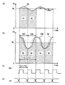
ここで、図5(a)は、合成信号CSwに含まれているセンサ変調信号Smを概念的に示し、図5(b)は、合成信号CSwを概念的に示す。また、図5(c)はサンプリング周期Tsを示し、図5(d)は、TAD41が出力するデジタルデータDTを示す。
Here, FIG. 5A conceptually shows the sensor modulation signal Sm included in the combined signal CSw, and FIG. 5B conceptually shows the combined signal CSw. FIG. 5C shows the sampling period Ts, and FIG. 5D shows the digital data DT output from the
加減算器42は、図5に示す前半サンプリング区間Sefの合成信号CSwの積分値と、後半サンプリング区間Sebの合成信号CSwの積分値との差を算出する。これは、図5(b)に示す面積S3−面積S4を算出していることを意味する。
The adder /
前半サンプリング区間Sefは、搬送波Cwの極大値から開始し、搬送波Cwの極小値までの区間である。また、センサ変調信号Smは搬送波Cwの位相と90度ずれているので、前半サンプリング区間Sefは、センサ変調信号Smの0度から180度までとなっている。 The first half sampling interval Sef is an interval starting from the local maximum value of the carrier wave Cw to the local minimum value of the carrier wave Cw. In addition, since the sensor modulation signal Sm is shifted by 90 degrees from the phase of the carrier wave Cw, the first half sampling period Sef is from 0 degrees to 180 degrees of the sensor modulation signal Sm.
後半サンプリング区間Sebは、搬送波Cwの極小値から開始し、搬送波Cwの極大値までの区間である。また、後半サンプリング区間Sebは、センサ変調信号Smの180度から360度までの区間である。 The latter half sampling interval Seb is an interval starting from the local minimum value of the carrier wave Cw to the local maximum value of the carrier wave Cw. Further, the latter half sampling interval Seb is an interval from 180 degrees to 360 degrees of the sensor modulation signal Sm.
搬送波Cwは正弦波であるため、前半サンプリング区間Sefにおける搬送波Cwの積分値と、後半サンプリング区間Sebにおける搬送波Cwの積分値とは等しい。したがって、前半サンプリング区間Sefの合成信号CSwの積分値と、後半サンプリング区間Sebの間の合成信号CSwの積分値との差を算出することで、搬送波Cwの成分が除去される。よって、この差は、センサ変調信号Smの検波値を表している。 Since the carrier wave Cw is a sine wave, the integrated value of the carrier wave Cw in the first half sampling period Sef is equal to the integrated value of the carrier wave Cw in the second half sampling period Seb. Therefore, the component of the carrier wave Cw is removed by calculating the difference between the integrated value of the synthesized signal CSw in the first half sampling period Sef and the integrated value of the synthesized signal CSw in the second half sampling period Seb. Therefore, this difference represents the detection value of the sensor modulation signal Sm.
また、面積S3−面積S4は、センサ変調信号Smにとっては、図5(a)に示す面積S1−面積S2を演算していることになる。これは、事実上、図5(a)に示す面積Saと面積Sbの和を算出していることになる。 Further, the area S3 to the area S4 is calculated from the area S1 to the area S2 shown in FIG. 5A for the sensor modulation signal Sm. In effect, this means that the sum of the area Sa and the area Sb shown in FIG.
次に、加減算器42が算出する上記和は、図5(b)に示す面積S3+面積S4を算出することを意味する。
図5(b)から分かるように、センサ変調信号Smにベース信号Sbaが合成されていないとき、すなわち、角速度が0であるときには、前半サンプリング区間Sefにおける合成信号CSwの積分値と後半サンプリング区間Sebにおける合成信号CSwの積分値との和の平均値は、搬送波Cwの中心レベルVbとなる。また、面積S3+面積S4は、センサ変調信号Smにとっては、図5(a)に示す面積Sa−面積Sbを算出していることになる。これらのことから、面積S3+面積S4は、面積Sc+面積Sdを算出していることになる。
Next, the sum calculated by the adder /
As can be seen from FIG. 5B, when the base signal Sba is not synthesized with the sensor modulation signal Sm, that is, when the angular velocity is 0, the integrated value of the synthesized signal CSw in the first half sampling period Sef and the second half sampling period Seb. The average value of the sum of the combined signal CSw and the integrated value becomes the center level Vb of the carrier wave Cw. Further, the area S3 + the area S4 is calculated as the area Sa−the area Sb shown in FIG. 5A for the sensor modulation signal Sm. From these things, area S3 + area S4 is calculating area Sc + area Sd.
ここで、面積S3+面積S4は、面積S1+面積S2に対応する値となり、上記のバイアス値を表す。
ところで、センサ変調信号Smの検波値は、温度等の外的要因によって変動することが知られている。このため、搬送波Cwの中心レベルVbを適宜補正するキャリブレーションを実施する必要がある。
Here, area S3 + area S4 is a value corresponding to area S1 + area S2, and represents the above-described bias value.
Incidentally, it is known that the detection value of the sensor modulation signal Sm varies depending on external factors such as temperature. For this reason, it is necessary to perform calibration for appropriately correcting the center level Vb of the carrier wave Cw.
そこで、デジタル補正回路50は、図6に示す補正回路処理を実施することによって、上記のキャリブレーションおよびセンサ変調信号Smからベース信号Sbaを抽出する処理を実施する。なお、補正回路処理は、デジタル補正回路50等のハードウェアで実現されてもよく、補正回路処理に相当するプログラムをCPUが実行するによるソフトウェアで実現されてもよい。
Therefore, the
[1−2.処理]
補正回路処理では、図6に示すように、まずS110にて、ジャイロセンサ装置1に与えられる角速度が0であるか否かを判定する。本実施形態の処理では、自車両の角速度が0であるか否かを判定する。例えば車速やパーキングブレーキの作動状態等、自車両が停止していることを判定するための情報を取得し、自車両が停止していることが認識できた場合に、自車両の角速度が0であると判定する。なお、ジャイロセンサ装置1が静止していること、すなわち、ベース信号が合成信号に合成されていないことを検知する他のセンサを用いて角速度が0であるか否かを判定してもよい。
[1-2. processing]
In the correction circuit processing, as shown in FIG. 6, first, in S110, it is determined whether or not the angular velocity given to the
角速度が0であれば、S120〜S160の処理にてキャリブレーションを実施する。また、角速度が0でなければ、S210〜S230の処理にて角速度(外力Sw)を抽出する処理を実施する。 If the angular velocity is 0, calibration is performed in the processing of S120 to S160. If the angular velocity is not 0, the processing of extracting the angular velocity (external force Sw) is performed in the processing of S210 to S230.
キャリブレーションでは、まず、S120、S130にて、バイアス値および検波値を取得する。なお、バイアス値および検波値は、加減算器42から取得する。
次に、S140にて、回帰直線を演算する。回帰直線とは、バイアス値と検波値との相関関係に応じて設定される一次関数を示す。発明者らは、バイアス値と検波値との間に、温度等の外的要因によらず、概ね一定の関係があることを見出した。
In the calibration, first, a bias value and a detection value are acquired in S120 and S130. The bias value and the detection value are acquired from the adder /
Next, in S140, a regression line is calculated. The regression line indicates a linear function set according to the correlation between the bias value and the detected value. The inventors have found that there is a generally constant relationship between the bias value and the detected value regardless of external factors such as temperature.
すなわち、バイアス値と検波値とが、傾きと切片とで規定される一次関数によってそれぞれの値を相互に変換できることを発見した。なお、一次関数をy=ax+bと表記した際に、傾きとは、aに対応する値であり、切片とはbに対応する値である。 That is, it has been found that the bias value and the detected value can be converted into each other by a linear function defined by the slope and the intercept. When the linear function is expressed as y = ax + b, the slope is a value corresponding to a, and the intercept is a value corresponding to b.
上記の発見により、バイアス値および検波値は、
(検波値)=(傾き)×(バイアス値)+(切片)…式(1)
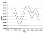
で表現できることが分かった。具体的には、図7に示す検波値Dの時間の経過に伴う変化と、図8に示すバイアス値Fの時間の経過による変化とを用いて、上記の回帰直線において関係式が正しく表現できているかを確認したグラフを図9に示す。なお、図7〜図9において2本の実線は、各値が変化する際の概ねの上限値および下限値を示し、これらの実線にて挟まれる間の領域が各値の概ねの変化幅(レンジ)となる。
Based on the above findings, the bias value and detection value are
(Detection value) = (slope) × (bias value) + (intercept) (1)
I understood that it can be expressed by. Specifically, the relational expression can be correctly expressed in the above regression line using the change of the detection value D shown in FIG. 7 with the passage of time and the change of the bias value F shown in FIG. 8 with the passage of time. FIG. 9 shows a graph for confirming whether or not this is the case. In FIG. 7 to FIG. 9, the two solid lines indicate the approximate upper limit value and lower limit value when each value changes, and the area between these solid lines indicates the approximate change width of each value ( Range).
また、図9においては、
(補正結果G)=(上記式(1)の左辺)/(上記式(1)の右辺)…式(2)
としている。
In FIG. 9,
(Correction result G) = (left side of the above formula (1)) / (right side of the above formula (1))... (2)
It is said.
補正結果Gは、図9において概ね0.998〜1.002の範囲内に収束しており、その誤差は約0.2%以下となる。この結果、バイアス値および検波値とが回帰直線において相互に変換できることが証明できた。 The correction result G converges in the range of approximately 0.998 to 1.002 in FIG. 9, and the error is about 0.2% or less. As a result, it was proved that the bias value and the detected value can be mutually converted in the regression line.
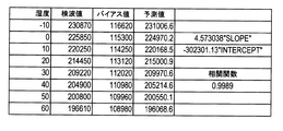
なお、図7〜図9においては、変動し得る室温において実験を行った例であるが、図10に示すように、複数の温度の際にも実験を行っている。図10では、温度を変更しつつ、検波値とバイアス値、加えてバイアス値から予測される検波値である予測値を記述している。何れの温度においても検波値と予測値との差は小さく、バイアス値および検波値とが回帰直線において相互に変換できることが分かる。 7 to 9 are examples in which the experiment was performed at a room temperature that could vary, but the experiment was also performed at a plurality of temperatures as shown in FIG. In FIG. 10, the detection value and the bias value as well as the predicted value that is the detection value predicted from the bias value are described while changing the temperature. It can be seen that the difference between the detected value and the predicted value is small at any temperature, and the bias value and the detected value can be converted to each other in the regression line.
実験を重ねるにつれて、傾きの値は概ね一定であり、切片のみに多少のばらつきが生じることも分かった。したがって本実施形態では、傾きの値については予め設定された固定値を用い、傾きを含む一次関数である上記式(1)にバイアス値と検波値とを代入することによって該一次関数における切片を算出する。 As the experiment was repeated, the value of the slope was generally constant, and it was also found that some variation occurred only in the intercept. Therefore, in this embodiment, a fixed value set in advance is used for the slope value, and the intercept in the linear function is obtained by substituting the bias value and the detected value into the above-described equation (1) that is a linear function including the slope. calculate.
続いて、S150にて、補正値を取得する。補正値としては、回帰直線における傾きおよび切片を取得する。
続いて、S160にて、バイアス値、補正値、バイアス値を回帰直線に代入することで求められる検波値に相当する値である検波相当値を演算し、この検波相当値を搬送波Cwの中心レベルVb(基準値)として保持する。搬送波Cwの中心レベルVbは、例えばEPROM60等、任意のメモリにおいて保持される。S160の処理が終了すると、キャリブレーションを終了し、補正回路処理を終了する。
Subsequently, in S150, a correction value is acquired. As the correction value, the slope and intercept in the regression line are acquired.
Subsequently, in S160, a detection equivalent value, which is a value corresponding to a detection value obtained by substituting the bias value, correction value, and bias value into the regression line, is calculated, and this detection equivalent value is calculated as the center level of the carrier wave Cw. This is held as Vb (reference value). The center level Vb of the carrier wave Cw is held in an arbitrary memory such as the
また、角速度を抽出する処理では、まずS210、S220にて、S120、S130の処理と同様に、バイアス値および検波値を取得する。続いて、S230にて、角速度を示す信号を抽出する。この処理では、検波値とメモリにて保持された基準値と差に基づいてベース信号を抽出する。すなわち、検波値と基準値と差が、角速度を示す信号の部位であるため、この差の値に応じて角速度を特定する。 In the process of extracting the angular velocity, first, in S210 and S220, the bias value and the detection value are acquired as in the processes of S120 and S130. Subsequently, in S230, a signal indicating the angular velocity is extracted. In this process, the base signal is extracted based on the difference between the detected value and the reference value held in the memory. That is, since the difference between the detected value and the reference value is a signal portion indicating the angular velocity, the angular velocity is specified according to the difference value.
S230の処理が終了すると、角速度を抽出する処理を終了し、補正回路処理を終了する。
[1−3.効果]
以上詳述した第1実施形態によれば、以下の効果が得られる。
When the process of S230 ends, the process of extracting the angular velocity ends, and the correction circuit process ends.
[1-3. effect]
According to the first embodiment described in detail above, the following effects can be obtained.
(1a)ジャイロセンサ装置1おいてセンサ回路部20は、合成信号を1周期分積分した値を表すバイアス値と、搬送波の極大値および極小値のいずれか一方をサンプリング開始時点とする半周期である前半の半周期において合成信号を積分した値と前半の半周期に続く後半の半周期において合成信号を積分した値との差を表す検波値と、の相関関係に応じて予め設定された補正値であって、バイアス値を検波値に相当する値を表す検波相当値に変換するための補正値を取得する(S150)。ベース信号が合成信号に合成されていないときにおいて、バイアス値を取得し(S120)、バイアス値と補正値とに基づいて検波相当値を演算し、該検波相当値を基準値として保持する(S160)。ベース信号が合成信号に合成されているときにおいて、検波値を取得し(S220)、検波値と基準値との差異に基づいてベース信号を抽出する(S230)。
(1a) In the
このような復調装置によれば、バイアス値から得られる検波相当値を搬送波における基準値として設定するので、合成信号からベース信号を復調する復調装置において、外的要因によらず、より正確にベース信号を復調することができる。 According to such a demodulator, the detection equivalent value obtained from the bias value is set as the reference value in the carrier wave. Therefore, in the demodulator that demodulates the base signal from the synthesized signal, the base signal is more accurately determined regardless of external factors. The signal can be demodulated.
(1b)上記のジャイロセンサ装置1においてデジタル補正回路50は、相関関係を一次関数で表す際において該一次関数の傾きを表す値を補正値として取得する。
このようなジャイロセンサ装置1によれば、相関関係を一次関数で表現するので、傾きを補正値とする簡素な構成で、より正確にベース信号を復調することができる。
(1b) In the
According to such a
(1c)上記のジャイロセンサ装置1においてデジタル補正回路50は、ベース信号が合成信号に合成されていないときにおいて、検波値を取得し、傾きを含む一次関数にバイアス値と検波値とを代入することによって該一次関数における切片を算出する。また、補正値として、傾きおよび切片を取得する。
(1c) In the
このようなジャイロセンサ装置1によれば、一次関数における切片を算出し、補正値として利用するので、より精度よくベース信号を復調することができる。また、傾きについては予め設定された値を取得し、切片のみを算出する構成とすることで、補正値を求める演算を簡素化することができる。
According to such a
(1d)上記のジャイロセンサ装置1においてデジタル補正回路50は、搬送波および変調信号の成分を含むアナログ信号をデジタルデータに変換することによって合成信号を生成するように構成されたAD変換回路(TAD41)を備える。
(1d) In the
このようなジャイロセンサ装置1によれば、デジタルデータである合成信号からベース信号を復調することができる。
(1e)上記のジャイロセンサ装置1においてAD変換回路は、複数のパルス信号遅延ユニットを直列接続したパルス遅延回路(リングゲート遅延回路413)を備え、アナログ信号を入力信号としてパルス遅延回路に入力し、搬送波の周期に応じて設定された時間毎に、パルス信号が通過したパルス信号遅延ユニットの数に基づいて、搬送波をデジタルデータに変換する。
According to such a
(1e) In the
このようなジャイロセンサ装置1によれば、一般的に温度特性が大きなパルス遅延回路を備えたAD変換回路でAD変換を行う構成であっても、搬送波における基準値として設定するので、合成信号からベース信号を復調する復調装置において、外的要因によらず、より正確にベース信号を復調することができる。
According to such a
[2.他の実施形態]
以上、本発明を実施するための形態について説明したが、本発明は上述の実施形態に限定されることなく、種々変形して実施することができる。
[2. Other Embodiments]
As mentioned above, although the form for implementing this invention was demonstrated, this invention is not limited to the above-mentioned embodiment, It can implement in various deformation | transformation.
(2a)上記実施形態では、S130,S220にて検波値を取得する構成としたが、例えば、S130,S220にて検波値を取得する処理のうちの少なくとも一方を省略する構成としてもよい。 (2a) In the above embodiment, the detection value is acquired in S130 and S220. However, for example, at least one of the processes for acquiring the detection value in S130 and S220 may be omitted.
S130の処理にて検波値の取得を省略する場合、予め回帰直線における傾きおよび切片をメモリにおいて保持しておけばよい。また、S230の処理にて検波値の取得を省略する場合、バイアス値から上記式(1)を用いて検波値を求めればよい。 When the acquisition of the detection value is omitted in the process of S130, the slope and intercept in the regression line may be stored in the memory in advance. Further, when the acquisition of the detection value is omitted in the process of S230, the detection value may be obtained from the bias value using the above formula (1).
これらのようにすれば、検波値を取得することなく、キャリブレーションまたはベース信号の復調を行うことができる。
(2b)上記実施形態では、搬送波Cwの極大値や極小値から始まる周期においてバイアス値や検波値を得るよう構成したが、搬送波Cwの極大値や極小値に限らず、任意のタイミングから半周期または1周期の検知を開始してもよい。
By doing so, calibration or demodulation of the base signal can be performed without obtaining a detection value.
(2b) In the above embodiment, the bias value and the detection value are obtained in the period starting from the maximum value and the minimum value of the carrier wave Cw. However, the half value is not limited to the maximum value and the minimum value of the carrier wave Cw, and a half cycle from any timing. Alternatively, one cycle of detection may be started.
(2c)上記実施形態における1つの構成要素が有する機能を複数の構成要素として分散させたり、複数の構成要素が有する機能を1つの構成要素に統合させたりしてもよい。また、上記実施形態の構成の一部を省略してもよい。また、上記実施形態の構成の少なくとも一部を、他の上記実施形態の構成に対して付加または置換してもよい。なお、特許請求の範囲に記載した文言のみによって特定される技術思想に含まれるあらゆる態様が本発明の実施形態である。 (2c) The functions of one component in the above embodiment may be distributed as a plurality of components, or the functions of a plurality of components may be integrated into one component. Moreover, you may abbreviate | omit a part of structure of the said embodiment. Further, at least a part of the configuration of the above embodiment may be added to or replaced with the configuration of the other embodiment. In addition, all the aspects included in the technical idea specified only by the wording described in the claim are embodiment of this invention.
(2d)上述したジャイロセンサ装置1の他、当該ジャイロセンサ装置1を構成要素とするシステム、当該ジャイロセンサ装置1としてコンピュータを機能させるためのプログラム、このプログラムを記録した半導体メモリ等の非遷移的実態的記録媒体、ジャイロセンサ装置1のキャリブレーション方法など、種々の形態で本発明を実現することもできる。
(2d) In addition to the above-described
[3.実施形態の構成と本発明の構成との対応関係]
上記実施形態においてセンサ回路部20は本発明でいう復調装置の一例に相当し、上記実施形態においてTAD41は本発明でいうAD変換回路の一例に相当する。また、上記実施形態においてデジタル補正回路50が実行する処理のうち、S120の処理は本発明でいうバイアス値取得部の一例に相当し、上記実施形態においてS130の処理は本発明でいう非合成取得部の一例に相当する。
[3. Correspondence between Configuration of Embodiment and Configuration of Present Invention]
In the above embodiment, the
また、上記実施形態においてS140の処理は本発明でいう切片算出部の一例に相当し、上記実施形態においてS150の処理は本発明でいう補正値取得部の一例に相当する。また、上記実施形態においてS160の処理は本発明でいう基準値保持部の一例に相当し、上記実施形態においてS220の処理は本発明でいう検波取得部の一例に相当する。 In the above embodiment, the process of S140 corresponds to an example of the intercept calculation unit referred to in the present invention. In the above embodiment, the process of S150 corresponds to an example of the correction value acquisition unit referred to in the present invention. In the above embodiment, the process of S160 corresponds to an example of the reference value holding unit referred to in the present invention. In the above embodiment, the process of S220 corresponds to an example of the detection acquisition unit referred to in the present invention.
また、上記実施形態においてS230の処理は本発明でいう信号抽出部の一例に相当する。また、上記実施形態においてセンサ変調信号Smは本発明でいう変調信号の一例に相当する。 In the above-described embodiment, the process of S230 corresponds to an example of a signal extraction unit referred to in the present invention. In the above embodiment, the sensor modulation signal Sm corresponds to an example of the modulation signal in the present invention.
1…ジャイロセンサ装置、10…エレメント、20…センサ回路部、30…自励共振駆動回路、31…リングオシレータ、32…TDC、33…DCO、34…制御回路、40…デジタル同期検波回路、42…加減算器、50…デジタル補正回路、60…EPROM、411…ゲート、412…インバータ、413…リングゲート遅延回路、414…カウンタ、415…ラッチ回路、416…パルスセレクタ、417…エンコーダ、418…信号処理回路。
DESCRIPTION OF
Claims (5)
前記搬送波に同期した半周期である前半の半周期において前記合成信号を積分した値と、前記前半の半周期に続く後半の半周期において前記合成信号を積分した値と、の差を表す検波値と、前記合成信号を1周期分積分した値を表すバイアス値と、の相関関係に応じて予め設定された補正値であって、前記バイアス値を前記検波値に相当する値を表す検波相当値に変換するための補正値を取得するように構成された補正値取得部(S150)と、
前記ベース信号が前記合成信号に合成されていないときにおいて、前記バイアス値を取得するように構成されたバイアス値取得部(S120)と、
前記バイアス値と前記補正値とに基づいて前記検波相当値を演算し、該検波相当値を基準値として保持するように構成された基準値保持部(S160)と、
前記ベース信号が前記合成信号に合成されているときにおいて、前記検波値を取得するように構成された検波取得部(S220)と、
前記検波値と前記基準値との差異に基づいて前記ベース信号を抽出するように構成された信号抽出部(S230)と、
を備えた復調装置。 A demodulator (20) configured to demodulate a base signal from a synthesized signal obtained by synthesizing a modulated signal obtained by modulating a base signal with respect to a carrier wave,
A detection value representing a difference between a value obtained by integrating the synthesized signal in the first half cycle which is a half cycle synchronized with the carrier wave, and a value obtained by integrating the synthesized signal in the second half cycle following the first half cycle. And a bias value representing a value obtained by integrating the synthesized signal for one period, and a correction value preset in accordance with the correlation, the bias value representing a value corresponding to the detected value A correction value acquisition unit (S150) configured to acquire a correction value for conversion to
A bias value acquisition unit (S120) configured to acquire the bias value when the base signal is not combined with the combined signal;
A reference value holding unit (S160) configured to calculate the detection equivalent value based on the bias value and the correction value, and hold the detection equivalent value as a reference value;
A detection acquisition unit (S220) configured to acquire the detection value when the base signal is combined with the combined signal;
A signal extraction unit (S230) configured to extract the base signal based on a difference between the detection value and the reference value;
A demodulator comprising:
前記補正値取得部は、前記相関関係を一次関数で表す際において該一次関数の傾きを表す値を前記補正値として取得する
ように構成された復調装置。 The demodulator according to claim 1,
The demodulation device configured to acquire, as the correction value, a value representing a slope of the linear function when the correlation value is expressed by a linear function.
前記ベース信号が前記合成信号に合成されていないときにおいて、前記検波値を取得するように構成された非合成取得部(S130)と、
前記傾きを含む一次関数に前記バイアス値と前記検波値とを代入することによって該一次関数における切片を算出するように構成された切片算出部(S140)と、
をさらに備え、
前記補正値取得部は、前記補正値として、前記傾きおよび前記切片を取得する
ように構成された復調装置。 The demodulator according to claim 1 or 2,
A non-synthesis acquisition unit (S130) configured to acquire the detection value when the base signal is not combined with the synthesis signal;
An intercept calculating unit (S140) configured to calculate an intercept in the linear function by substituting the bias value and the detected value into a linear function including the slope;
Further comprising
The demodulation device configured to acquire the inclination and the intercept as the correction value.
前記搬送波および前記変調信号の成分を含むアナログ信号をデジタルデータに変換することによって前記合成信号を生成するように構成されたAD変換回路(41)、
をさらに備えた復調装置。 The demodulator according to any one of claims 1 to 3,
An AD conversion circuit (41) configured to generate the composite signal by converting an analog signal including the carrier wave and the component of the modulation signal into digital data;
A demodulator further comprising:
前記AD変換回路は、複数のパルス信号遅延ユニットを直列接続したパルス遅延回路(413)を備え、前記アナログ信号を入力信号として前記パルス遅延回路に入力し、前記搬送波の周期に応じて設定された時間毎に、パルス信号が通過した前記パルス信号遅延ユニットの数に基づいて、前記搬送波をデジタルデータに変換する
ように構成された復調装置。 The demodulator according to claim 4, wherein
The AD conversion circuit includes a pulse delay circuit (413) in which a plurality of pulse signal delay units are connected in series, and the analog signal is input to the pulse delay circuit as an input signal, and is set according to the period of the carrier wave A demodulator configured to convert the carrier wave into digital data based on the number of the pulse signal delay units through which a pulse signal has passed every time.
Priority Applications (1)
| Application Number | Priority Date | Filing Date | Title |
|---|---|---|---|
| JP2016080570A JP6701906B2 (en) | 2016-04-13 | 2016-04-13 | Demodulator |
Applications Claiming Priority (1)
| Application Number | Priority Date | Filing Date | Title |
|---|---|---|---|
| JP2016080570A JP6701906B2 (en) | 2016-04-13 | 2016-04-13 | Demodulator |
Publications (2)
| Publication Number | Publication Date |
|---|---|
| JP2017191007A true JP2017191007A (en) | 2017-10-19 |
| JP6701906B2 JP6701906B2 (en) | 2020-05-27 |
Family
ID=60084857
Family Applications (1)
| Application Number | Title | Priority Date | Filing Date |
|---|---|---|---|
| JP2016080570A Expired - Fee Related JP6701906B2 (en) | 2016-04-13 | 2016-04-13 | Demodulator |
Country Status (1)
| Country | Link |
|---|---|
| JP (1) | JP6701906B2 (en) |
Citations (3)
| Publication number | Priority date | Publication date | Assignee | Title |
|---|---|---|---|---|
| US20050047526A1 (en) * | 2003-08-29 | 2005-03-03 | Takamoto Watanabe | Synchronous detection method and device |
| JP2006047144A (en) * | 2004-08-05 | 2006-02-16 | Denso Corp | Vibration type angular velocity sensor |
| US20130099836A1 (en) * | 2011-10-25 | 2013-04-25 | Invensense, Inc. | Gyroscope with phase and duty-cycle locked loop |
-
2016
- 2016-04-13 JP JP2016080570A patent/JP6701906B2/en not_active Expired - Fee Related
Patent Citations (4)
| Publication number | Priority date | Publication date | Assignee | Title |
|---|---|---|---|---|
| US20050047526A1 (en) * | 2003-08-29 | 2005-03-03 | Takamoto Watanabe | Synchronous detection method and device |
| JP2005102129A (en) * | 2003-08-29 | 2005-04-14 | Denso Corp | Synchronous detection method and apparatus |
| JP2006047144A (en) * | 2004-08-05 | 2006-02-16 | Denso Corp | Vibration type angular velocity sensor |
| US20130099836A1 (en) * | 2011-10-25 | 2013-04-25 | Invensense, Inc. | Gyroscope with phase and duty-cycle locked loop |
Also Published As
| Publication number | Publication date |
|---|---|
| JP6701906B2 (en) | 2020-05-27 |
Similar Documents
| Publication | Publication Date | Title |
|---|---|---|
| JP2013003141A (en) | Gyroscope dynamic motor amplitude compensation for enhanced rate estimation during startup | |
| JP2011033602A (en) | Resolver/digital converter, and resolver/digital conversion method | |
| US20170115318A1 (en) | Semiconductor device, electronic control system, and automobile | |
| JP5601292B2 (en) | Digital phase synchronization circuit and physical quantity detection sensor | |
| JP6665070B2 (en) | Motor control device and method for detecting current ripple of DC motor | |
| JP2013198114A (en) | Clock phase error detection device and method | |
| EP2077621B1 (en) | Reference signal generation circuit, angle converter, and angle detection apparatus | |
| JP6380229B2 (en) | Demodulator | |
| JP2010151669A (en) | Physical quantity detection circuit and physical quantity sensor device | |
| JP6701906B2 (en) | Demodulator | |
| JP2018072271A (en) | Self-excited resonance circuit | |
| JP5729323B2 (en) | Self-excited resonant circuit | |
| JP4237197B2 (en) | Rotation angle detector | |
| JP6214480B2 (en) | Frequency response measuring device | |
| JP6665686B2 (en) | Demodulator | |
| JP6610939B2 (en) | Time synchronization method, vibration sensor, vibration detection device, program, and recording medium | |
| JP2019086410A5 (en) | ||
| US9614513B2 (en) | Vibration generation apparatus | |
| CA3025654C (en) | System and method for providing the amplitude and phase delay of a sinusoidal signal | |
| JP2009216617A (en) | Sampling clock generation circuit and alternating current signal measuring device | |
| KR100980168B1 (en) | Phase difference detection device and rotation position detection device | |
| JPH08146160A (en) | Time counting device | |
| JP6112832B2 (en) | Angle correction device and rotation angle sensor | |
| JP2010230439A (en) | Control circuit | |
| JP6657499B2 (en) | Frame synchronization apparatus, measurement apparatus including the same, frame synchronization method and measurement method |
Legal Events
| Date | Code | Title | Description |
|---|---|---|---|
| A621 | Written request for application examination |
Free format text: JAPANESE INTERMEDIATE CODE: A621 Effective date: 20190304 |
|
| A977 | Report on retrieval |
Free format text: JAPANESE INTERMEDIATE CODE: A971007 Effective date: 20200108 |
|
| A131 | Notification of reasons for refusal |
Free format text: JAPANESE INTERMEDIATE CODE: A131 Effective date: 20200121 |
|
| A521 | Request for written amendment filed |
Free format text: JAPANESE INTERMEDIATE CODE: A523 Effective date: 20200305 |
|
| TRDD | Decision of grant or rejection written | ||
| A01 | Written decision to grant a patent or to grant a registration (utility model) |
Free format text: JAPANESE INTERMEDIATE CODE: A01 Effective date: 20200407 |
|
| A61 | First payment of annual fees (during grant procedure) |
Free format text: JAPANESE INTERMEDIATE CODE: A61 Effective date: 20200420 |
|
| R151 | Written notification of patent or utility model registration |
Ref document number: 6701906 Country of ref document: JP Free format text: JAPANESE INTERMEDIATE CODE: R151 |
|
| R250 | Receipt of annual fees |
Free format text: JAPANESE INTERMEDIATE CODE: R250 |
|
| LAPS | Cancellation because of no payment of annual fees |