JP2017183670A5 - - Google Patents
Download PDFInfo
- Publication number
- JP2017183670A5 JP2017183670A5 JP2016073336A JP2016073336A JP2017183670A5 JP 2017183670 A5 JP2017183670 A5 JP 2017183670A5 JP 2016073336 A JP2016073336 A JP 2016073336A JP 2016073336 A JP2016073336 A JP 2016073336A JP 2017183670 A5 JP2017183670 A5 JP 2017183670A5
- Authority
- JP
- Japan
- Prior art keywords
- flow path
- frame
- wall
- metal plate
- electronic device
- Prior art date
- Legal status (The legal status is an assumption and is not a legal conclusion. Google has not performed a legal analysis and makes no representation as to the accuracy of the status listed.)
- Granted
Links
- 229910052751 metal Inorganic materials 0.000 claims description 75
- 239000002184 metal Substances 0.000 claims description 75
- 238000001816 cooling Methods 0.000 claims description 53
- 230000002093 peripheral Effects 0.000 claims description 49
- 239000011347 resin Substances 0.000 claims description 6
- 229920005989 resin Polymers 0.000 claims description 6
- 230000003287 optical Effects 0.000 description 19
- XEEYBQQBJWHFJM-UHFFFAOYSA-N iron Chemical compound [Fe] XEEYBQQBJWHFJM-UHFFFAOYSA-N 0.000 description 4
- 238000007599 discharging Methods 0.000 description 3
- 229910052782 aluminium Inorganic materials 0.000 description 2
- XAGFODPZIPBFFR-UHFFFAOYSA-N aluminum Chemical compound [Al] XAGFODPZIPBFFR-UHFFFAOYSA-N 0.000 description 2
- 229910052742 iron Inorganic materials 0.000 description 2
- 229920000122 Acrylonitrile butadiene styrene Polymers 0.000 description 1
- 210000000078 Claw Anatomy 0.000 description 1
- 239000004793 Polystyrene Substances 0.000 description 1
- 230000000875 corresponding Effects 0.000 description 1
- 238000010586 diagram Methods 0.000 description 1
- 238000003780 insertion Methods 0.000 description 1
- 230000004048 modification Effects 0.000 description 1
- 238000006011 modification reaction Methods 0.000 description 1
- 229920002223 polystyrene Polymers 0.000 description 1
- 230000001629 suppression Effects 0.000 description 1
- 230000000007 visual effect Effects 0.000 description 1
Images
Description
本発明は電子機器の通気口の構造に関する。 The present invention relates to a structure of a vent of an electronic device.
下記特許文献1の電子機器は、電子機器が備えている種々の部品が取り付けられているフレームと、フレームの上側を覆っている上カバーと、フレームの下側を覆っている下カバーとを有している。フレームは、電子機器が備えている種々の部品(具体的には冷却ファン、ヒートシンク、電源ユニット、光ディスクドライブなど)を取り囲むように形成されている外周部を有している。冷却ファンとヒートシンクの上側に回路基板が配置されている。回路基板は金属によって形成されているシャーシによって覆われている。
The electronic device disclosed in
特許文献1の電子機器ではフレームの全体が樹脂で形成されている。フレームの剛性を向上するためには、フレームの厚さや太さを増す必要が生じる。このことは電子機器の小型化を図る上で好ましくない。
In the electronic device of
本発明の目的の一つは、電子機器の小型化を図りながら、且つフレームの剛性を向上できる電子機器を提供することにある。 One of the objects of the present invention is to provide an electronic device capable of improving the rigidity of the frame while reducing the size of the electronic device.
本発明に係る電子機器は、複数の部品と、前記複数の部品を取り囲んでいる外周部を有している、樹脂によって形成されているフレームと、前記複数の部品に対して第1の方向における一方側に配置されている回路基板と、前記複数の部品に対して前記第1の方向における前記一方側に配置され、前記フレームに取り付けられている、金属によって形成されているシャーシと、前記複数の部品のうちの少なくとも一つの部品に対して前記第1の方向における他方側に配置され、前記フレームに取り付けられている金属プレートと、を有している。 An electronic apparatus according to the present invention includes a plurality of components, a frame formed of a resin having an outer peripheral portion surrounding the plurality of components, and a first direction with respect to the plurality of components. A circuit board disposed on one side, a chassis formed of metal, disposed on the one side in the first direction with respect to the plurality of components, and attached to the frame; A metal plate disposed on the other side in the first direction with respect to at least one of the components, and attached to the frame.
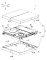
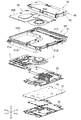
以下、本発明の一実施形態について図面を参照しながら説明する。図1は本発明の一実施形態に係る電子機器1の斜視図である。図2は電子機器1の分解斜視図である。図3は図2に示される本体10の分解斜視図である。図4Aは本体10の平面図である。図4Bは下カバー60が取り付けられているフレーム20の平面図である。図5は図4AのV−V線で示される切断面で得られる電子機器1の断面図である。図6は図3に示される金属プレート39、フレーム20、冷却ファン5の斜視図である。
Hereinafter, an embodiment of the present invention will be described with reference to the drawings. FIG. 1 is a perspective view of an
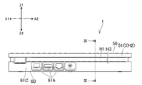
以下の説明では、図1に示すX1及びX2をそれぞれ左方向及び右方向とし、Y1及びY2をそれぞれ前方及び後方とし、Z1及びZ2をそれぞれ上方及び下方とする。 In the following description, X1 and X2 shown in FIG. 1 are the left direction and the right direction, respectively, Y1 and Y2 are the front and rear, respectively, and Z1 and Z2 are the upper and lower directions, respectively.
電子機器1は、例えばゲーム装置やオーディオ・ビジュアル機器として機能するエンタテインメント装置である。電子機器1は、ゲームプログラムの実行により生成した動画像データや、光ディスクなどの記録媒体から取得した映像・音声データ及び/又はネットワークを通して取得した映像・音声データをテレビジョンなどの表示装置に出力する。電子機器1はゲーム装置などのエンタテインメント装置に限られず、パーソナルコンピュータでもよい。
The
図2に示すように、電子機器1は本体10を有している。本体10の上側は電子機器1の外装部材Aを構成する上カバー50によって覆われている。本体10の下側は外装部材Aを構成する下カバー60によって覆われている。図3に示すように、本体10はフレーム20と、フレーム20に取り付けられる種々の部品とによって構成されている。後述するように、電子機器1の例では、フレーム20も外装部材Aを構成している。
As shown in FIG. 2, the
図3に示すように、フレーム20には、例えば冷却ファン5、光ディスクドライブ7、及び電源ユニット40などが取り付けられる。電子機器1の例では、冷却ファン5と光ディスクドライブ7は電子機器1の前部に配置され、左右方向で並んでいる。電源ユニット40は冷却ファン5と光ディスクドライブ7の後方に配置されている。電源ユニット40はケース42を有している。ケース42には電源回路が実装された回路基板41(図5参照)が収容されている。電子機器1が備えている部品のレイアウト、すなわち冷却ファン5、光ディスクドライブ7、及び電源ユニット40のレイアウトは、電子機器1の例に限られない。また、電子機器1は必ずしもこれらの部品の全てを有していなくてもよい。例えば、電子機器1は光ディスクドライブ7を有していなくてもよい。
As shown in FIG. 3, for example, the
図3に示すように、フレーム20はフレーム外周部21を有している。フレーム外周部21は電子機器1が備えている複数の部品を取り囲んでいる。電子機器1の例では、フレーム外周部21は、上述した光ディスクドライブ7、冷却ファン5、及び電源ユニット40を取り囲んでいる(図4A参照)。フレーム外周部21は平面視において略四角形であり、前壁部21Aと、右壁部21Bと、後壁部21Cと、左壁部21Dとを有している。前壁部21Aは上述の部品に対して前方に位置している壁部である。前壁部21Aには光ディスクドライブ7に光ディスクを挿入するための挿入口21nが形成されてもよい。後壁部21Cは前壁部21Aとは反対側に位置する壁部である。右壁部21Bは上述の部品に対して右方向に位置し、左壁部21Dは右壁部21Bとは反対側に位置する壁部である。フレーム外周部21の内側は上下方向に開口している。すなわち、フレーム外周部21は筒状である。
As shown in FIG. 3, the
図3に示すように、本体10は回路基板31、上シャーシ32、及び下シャーシ33を含んでいる。シャーシ32、33は、アルミニウムや鉄などの金属の板によって構成され、回路基板31の上面及び下面をそれぞれ覆っている。回路基板31には、電子機器1を制御したり画像処理を実行する集積回路などの電子部品が実装されている。シャーシ32、33は集積回路等の部品から出る電磁波の輻射を防止したり、外部装置からの電磁波が回路基板31上の電子部品に影響するのを防止している。一例では、シャーシ32、33は回路基板31の全体を覆う。シャーシ32、33は、回路基板31において集積回路31a等の部品が実装されている領域だけを覆ってもよい。
As shown in FIG. 3, the
回路基板31とシャーシ32、33はフレーム外周部21の内側に配置されている上述の部品の下側に配置されている。電子機器1の例では、回路基板31とシャーシ32、33は冷却ファン5と電源ユニット40の下側に位置している(図5参照)。回路基板31とシャーシ32、33はフレーム20に取り付けられる。より具体的には、回路基板31とシャーシ32、33はフレーム外周部21に取り付けられている。電子機器1の例では、回路基板31とシャーシ32、33はフレーム外周部21の前壁部21A、右壁部21B、後壁部21Cに取り付けられている。回路基板31とシャーシ32、33の取り付けには、例えばビスなどの固定具が利用される。電子機器1は必ずしも2枚のシャーシ32、33を有していなくてもよい。すなわち、回路基板31の一方の面にだけシャーシが設けられてもよい。
The
図3に示すように、電子機器1はヒートシンク34を有している。ヒートシンク34は回路基板31に実装されている集積回路31a(図5参照)等の発熱部品に直接的に又は間接的に接触している。ヒートシンク34は、冷却ファン5から続く後述する空気流路S2(図4A参照)に配置されている。電子機器1の例では、ヒートシンク34は上シャーシ32に取り付けられている。詳細には、図5に示すように、ヒートシンク34はベース部34aと、ベース部34aの上側に固定されている複数のフィン34bとを有している。上シャーシ32にはヒートシンク34に対応したサイズの穴が形成され、ヒートシンク34のフィン34bは上シャーシ32の穴に下側から嵌められている。そして、ベース部34aがシャーシ32の穴の縁に固定されている。フィン34bは上シャーシ32の上側に位置し、空気流路S2に位置している。ヒートシンク34の取り付け構造は電子機器1の例に限られず、適宜変更されてよい。
As shown in FIG. 3, the
図3に示すように、電子機器1は金属プレート39を有している。金属プレート39は冷却ファン5を挟んで、シャーシ32、33と回路基板31とは反対側に配置されている。電子機器1の例では、金属プレート39は冷却ファン5の上側に配置されている。また、金属プレート39はフレーム20に取り付けられている。具体的には、金属プレート39はフレーム外周部21に取り付けられている。フレーム20はABS樹脂やポリスチレンなどの樹脂で形成されている。一方、プレート39はアルミニウムや鉄などの金属によって形成されている。金属プレート39を利用するこのような構造によれば、フレーム20の壁部21A、21B、21C、21Dの厚さを増すことなく、フレーム20の剛性を向上できる。
As shown in FIG. 3, the
金属プレート39はフレーム外周部21を構成している4つの壁部21A、21B、21C、21Dのうち少なくとも3つに取り付けられるのが好ましい。こうすることによって、フレーム外周部21の剛性をより効果的に向上できる。図6に示すように、電子機器1の例では、金属プレート39は、フレーム外周部21の右壁部21Bと、前壁部21Aと、左壁部21Dとに取り付けられている。一例では、金属プレート39はフレーム外周部21の上縁に取り付けられる。他の例として、フレーム外周部21の内側に取付部が形成され、この取付部に金属プレート39が取り付けられてもよい。金属プレート39の取付には、例えば、ビスなどの固定具が利用される。
The
金属プレート39の取り付け構造は、ここで説明する例に限られない。例えば、金属プレート39はフレーム外周部21の4つの壁部21A、21B、21C、21Dのうち2つにだけ取り付けられてもよい。後において説明するように、金属プレート39は冷却ファン5を覆い、空気流路を規定する壁として機能している。したがって、金属プレート39は、冷却ファン5に近い2つの壁部(電子機器1の例では、前壁部21A及び右壁部21B)にだけ取り付けられてもよい。さらに他の例として、金属プレート39は4つの壁部21A、21B、21C、21Dの全部に取り付けられてもよい。この場合、金属プレート39はフレーム外周部21の内側に配置されている部品の全部を覆ってもよいし、フレーム外周部21の内側に配置されている部品の一部だけを覆ってもよい。
The attachment structure of the
上述したように、電子機器1はフレーム外周部21の内側に配置される冷却ファン5とヒートシンク34とを有している。また、電子機器1は通気口E1、E2を有している(図9参照)。ここで「通気口」とは、電子機器1の外装部材Aの外部と内部との境界である。すなわち、通気口E1、E2の外部には外気が存在し、外装部材A内の空気は通気口E1、E2を通り過ぎた瞬間に外気となる。電子機器1は、通気口E1、E2として、外装部材A内の空気を外部に排出するための排気口を有している。電子機器1の例では、排気口E1、E2はフレーム外周部21の後壁部21Cに設けられている。フレーム外周部21の内側には、冷却ファン5から排気口E1、E2に続く空気流路S1、S2、S3が形成されている(図4A参照)。
As described above, the
電子機器1の例では、冷却ファン5はその回転中心線C1(図6参照)が上下方向に沿うように配置されている。図4Aに示すように、空気流路は冷却ファン5の外周に形成され円弧状に湾曲している第1流路S1と、冷却ファン5の後側に形成され第1流路S1に接続している第2流路S2とを有している。第2流路S2にヒートシンク34が配置されている。空気流路は、さらに、ヒートシンク34の後側に形成され第2流路S2に接続している第3流路S3を有している。上述したように、電子機器1はその後部に電源ユニット40を有している。電源ユニット40は回路基板41と、回路基板41を収容しているケース42とを有している。第3流路S3はケース42によって構成されており、回路基板41は第3流路S3に配置されている(図5参照)。ケース42の後側に排気口E1、E2が設けられている。回路基板41には電源回路が実装されている。電源回路は電子機器1が備えている種々の部品にその駆動電力を供給する。
In the example of the
冷却ファン5が駆動するとき、冷却ファン5から第1流路S1に空気が流れ出す。その後、空気は第2流路S2に流れ、ヒートシンク34を通過する。そして、空気は第3流路S3に流れる。すなわち、空気は電源ユニット40のケース42に流れ込む。その後、空気は排気口E1、E2から外部に排出される。
When the cooling
金属プレート39とフレーム20は、空気流路を規定する壁として機能する部分を有している。すなわち、金属プレート39とフレーム20は、空気流路の内側と外側とを区画する壁として機能する部分を有している。電子機器1の例では、金属プレート39とフレーム20は第1流路S1と第2流路S2を規定する壁として機能する部分を有している。このように、金属プレート39はフレーム20の剛性を向上する機能と、流路S1、S2を規定する壁としての機能とを有している。これによって、流路S1、S2の上壁を規定する専用の部材が不要となる。その結果、部品数を低減できる。また、その専用部材の分だけ電子機器の高さを低減できる。
The
図4B及び図6に示すように、フレーム20は第1流路S1と第2流路S2とを規定する流路壁部22を有している。流路壁部22は、平面視における流路S1、S2の外形を規定する壁である。流路壁部22は平面視において冷却ファン5とヒートシンク34を取り囲んでいる。
As shown in FIGS. 4B and 6, the
電子機器1の例では、流路壁部22は、冷却ファン5の外周を取り囲み冷却ファン5の外周に沿って湾曲している湾曲壁部22Aを有している。冷却ファン5と湾曲壁部22Aとの間に第1流路S1が形成されている。湾曲壁部22Aの一方の端部(電子機器1の例では、右端部)はフレーム外周部21の右壁部21Bに接続している。したがって、右壁部21Bの前部は流路壁部22の一部22Bとして機能している(部分22Bを以下では第1側壁部と称する)。流路壁部22は、湾曲壁部22Aの他方の端部(電子機器1の例では、左端部)から後方に伸びている第2側壁部22Cを有している。第1側壁部22Bと第2側壁部22Cとの間に第2流路S2が形成されている。流路壁部22の内側は上下方向に開口している。
In the example of the
図6に示すように、金属プレート39は、第1流路S1と第2流路S2の上側の壁として機能する部分39Aを有している(以下では、この部分39Aを流路上壁部と称する)。すなわち、流路上壁部39Aは流路S1、S2の上側を閉じている。流路上壁部39Aは、第1流路S1の上側の壁として機能する第1壁部39Aaと、第2流路S2の上側の壁として機能する第2壁部39Abとを有している。第2壁部39Abはヒートシンク34を覆っている。
As shown in FIG. 6, the
図6に示すように、冷却ファン5は、その底部に、フレーム外周部21の下側に取り付けられる取付プレート5cを有している。取付プレート5cは第1流路S1の下側を閉じており、第1流路S1の下側の壁として機能している。また、上述したように、フレーム外周部21の下側には上シャーシ32が取り付けられている。上シャーシ32は第2流路S2の下側の壁として機能する部分を有している。したがって、流路S1、S2は、フレーム20と金属プレート39と上シャーシ32と取付プレート5cとによって、周りに空間から区画されている。
As shown in FIG. 6, the cooling
金属プレート39の流路上壁部39Aはフレーム20の流路壁部22に接続している。すなわち、流路上壁部39Aは流路壁部22の上縁の全体(すなわち、湾曲壁部22A、側壁部22B、22Cの上縁)に接続している。このことによって、流路S1、S2の空気が流路S1、S2の外側に漏れることが抑えられている。電子機器1の例では、図6に示すように、フレーム20は流路壁部22とフレーム外周部21とに沿って配置される複数の取付部22aを有している。金属プレート39がフレーム20の流路壁部22上に配置され、ビスなどの固定具によって取付部22aに取り付けられている。これによって、金属プレート39の流路上壁部39Aはフレーム20の流路壁部22の上縁に密着している。
The upper flow
図7は図5で符号VIIで示す領域の拡大図である。図7に示すように、金属プレート39はフレーム20の流路壁部22上に位置している縁を有している。フレーム20の流路壁部22の上縁には、金属プレート39の縁に沿って形成され且つ金属プレート39の縁の外側に位置している凸部22bが形成されている。凸部22bは金属プレート39の縁を取り囲んでいる。電子機器1の例では、金属プレート39が有している第1壁部39Aaの前縁39d(図6参照)と第2壁部39Abの右縁39e(図6参照)は、フレーム20の流路壁部22(より具体的には、湾曲壁部22Aと第1側壁部22B)上に位置している。湾曲壁部22Aと第1側壁部22Bの上縁に凸部22bが形成されている。凸部22bは金属プレート39の縁39d、39eに沿って形成され、金属プレート39の縁39d、39eの外側に位置している。この凸部22bによって金属プレート39の縁39d、39eと流路壁部22の上縁との間から空気が漏れることを、より効果的に抑えることができる。
FIG. 7 is an enlarged view of a region indicated by reference numeral VII in FIG. As shown in FIG. 7, the
図6に示すように、冷却ファン5はロータ5aと、ロータ5aと一体的に回転する複数のフィン5bとを有している。フィン5bはロータ5aから半径方向に伸びている。金属プレート39の第1壁部39Aaには、複数のフィン5bの基部の上側を覆うフィンカバー部39cが設けられている。電子機器1の例では、フィンカバー部39cは環状に形成されている。ロータ5aは平面視においてフィンカバー部39cの内側に位置している。すなわち、ロータ5aの上方には金属プレート39が存在していない。こうすることによって、金属プレート39の厚さだけ電子機器1の高さを低減することが可能となっている。金属プレート39の形状はこれに限られない。例えば、フィンカバー部39cは金属プレート39に設けられていなくてもよい。金属プレート39はロータ5aの上側を覆う部分を有してもよい。
As shown in FIG. 6, the cooling
図6に示すように、フィンカバー部39cと第1壁部39Aaとの間には段差が形成されている。より具体的には、第1壁部39Aaの位置はフィンカバー部39cの位置よりも低い。第1壁部39Aaの内周縁とフィンカバー部39cの外周縁との間に開口39hが形成されている。冷却ファン5が駆動するときに、外部の空気はこの開口39hを通して冷却ファン5に流れる。第1壁部39Aaの位置とフィンカバー部39cの位置とが上下方向においてずれている上述の構造によれば、開口39hのサイズが確保し易くなる。その結果、吸気効率を向上できる。フィンカバー部39cの外周縁は周方向に並んでいる複数の接続部39fを介して第1壁部39Aaの内周縁に接続している。
As shown in FIG. 6, a step is formed between the fin cover portion 39c and the first wall portion 39Aa. More specifically, the position of the first wall portion 39Aa is lower than the position of the fin cover portion 39c. An opening 39h is formed between the inner peripheral edge of the first wall portion 39Aa and the outer peripheral edge of the fin cover portion 39c. When the cooling
図1に示すように、電子機器1はその外装部材Aに、外部の空気を導入するための吸気口P1を有している。電子機器1の例では、電子機器1の右側面と左側面とに吸気口P1が設けられている。詳細には、上カバー50の右壁部51Bと下カバー60の右壁部61Bは上下方向で離れて位置しており、それらの間に吸気口P1が形成されている。フレーム外周部21の右壁部21Bと上カバー50の右壁部51Bとの間には空気流路が形成されており、吸気口P1から導入された空気はフレーム外周部21の右壁部21Bと上カバー50の右壁部51Bとの間を通って、冷却ファン5の上側に向かって流れる。同様に、フレーム外周部21の右壁部21Bと下カバー60の右壁部61Bには空気流路が形成されており、吸気口P1から導入された空気はフレーム外周部21の右壁部21Bと下カバー60の右壁部61Bとの間を通って、冷却ファン5の下側に向かって流れる。冷却ファン5の下側に達した空気は、取付プレート5cに形成されている開口5dを通して、冷却ファン5に導入される。電子機器1の左側にも右側と同様に、吸気口が設けられている。上カバー50の左壁部と下カバー60の左壁部は上下方向で離れて位置し、それらの間に吸気口が形成されている。吸気口の位置は電子機器1の例に限られず、適宜変更されてよい。
As shown in FIG. 1, the
金属プレート39は、冷却ファン5とヒートシンク34など空気流路に配置される部品とは、異なる部品を覆う部分を有してもよい。電子機器1の例では、電子機器1の前部に光ディスクドライブ7が配置されている。図6に示すように、金属プレート39は光ディスクドライブ7を覆う部分39Bを有している(以下ではこの部分39Bを部品カバー部と称する)。電子機器1の例では、光ディスクドライブ7は、その上面の上側に、光ディスクの搬送する機構の一部を有している。部品カバー部39Bはこの機構を覆っている。このように金属プレート39で光ディスクドライブ7を覆うことによって、光ディスクドライブ7を覆う専用のカバーが不要となる。その結果、部品数を低減できる。また、その専用カバーの分だけ電子機器の高さを低減できる。
The
部品カバー部39Bが覆う部品は、光ディスクドライブ7に限られない。或いは、金属プレート39は部品カバー部39Bを有していなくてよい。すなわち、金属プレート39の全体が流路上壁部39Aとして機能してもよい。
The component covered by the
上述したように、空気流路は第2流路S2に続く第3流路S3を含んでいる。第3流路S3を規定する壁は電源ユニット40のケース42によって構成されている。金属プレート39の流路上壁部39Aとフレーム20の流路壁部22は、ケース42に形成されている通気口42dに接続している。電子機器1の例では、通気口42dはケース42の前面に形成されている(図3参照)。図5に示すように、金属プレート39の流路上壁部39Aの後縁39gは通気口42dの上縁に接続している。フレーム20の側壁部22B、22Cは通気口42dの左右の縁に接続している。このことによって、第2流路S2と第3流路S3との間で空気が外側に漏れることを、抑えることができる。
As described above, the air flow path includes the third flow path S3 following the second flow path S2. The wall that defines the third flow path S3 is constituted by a
上述したように、電子機器1は、その外装部材Aとして、本体10の上側を覆う上カバー50と、本体10の下側を覆う下カバー60とを有している。また、電子機器1の例では、上カバー50と下カバー60との間からフレーム20の一部が外部に露出している。詳細には、上カバー50は、電子機器1の平面視においてフレーム外周部21の外周を取り囲む周壁部51を有している。下カバー60は、電子機器1の平面視においてフレーム外周部21の外周を取り囲む周壁部61を有している。上カバー50の周壁部51の下縁と下カバー60の周壁部61の上縁は上下方向において離れており、フレーム外周部21は上カバー50の周壁部51の下縁と下カバー60の周壁部61の上縁との間から外部に露出している。したがって、電子機器1においては、外装部材Aはカバー50、60とフレーム20とによって構成されている。
As described above, the
外装部材Aは、上述した空気流路S1、S2,S3を通過した空気を外部に排出するための排気口E1、E2を有している。図8から図10は排気口E1、E2の構造を説明するための図である。図8は電子機器1の背面図である。図9は図8のIX−IX線で示す切断面で得られる断面図である。図10はフレーム20、電源ユニット40、下カバー60の後側を示す斜視図である。
The exterior member A has exhaust ports E1 and E2 for discharging the air that has passed through the air flow paths S1, S2, and S3 to the outside. 8 to 10 are diagrams for explaining the structure of the exhaust ports E1 and E2. FIG. 8 is a rear view of the
電子機器1の例では、電源ユニット40のケース42は、その後側に開口42fを有している(図10参照)。図9に示すように、外装部材Aはケース42の後方に排気口E1、E2を有している。ケース42内の空気(第3流路S3の空気)は、排気口E1、E2を通して外部に排出される。
In the example of the
図9に示すように、外装部材Aには、電源ユニット40の後方に位置している複数の遮蔽部が設けられている。電子機器1の例では、外装部材Aには3つの遮蔽部H1、H2、H3が設けられている(以下では、3つの遮蔽部を識別する場合、それぞれ第1遮蔽部H1、第2遮蔽部H2、第3遮蔽部H3と称する)。各遮蔽部H1、H2、H3は左右方向に伸びている細長い板状の部位である。電子機器1の例では、遮蔽部H1、H2、H3は電子機器1の左右方向の幅と概ね対応した長さを有している。
As shown in FIG. 9, the exterior member A is provided with a plurality of shielding portions located behind the
電子機器1の例では、図9に示すように、第1遮蔽部H1はフレーム20の後壁部21Cに設けられている。第2遮蔽部H2は上カバー50の周壁部51を構成している後壁部51Cと、フレーム20の後壁部21Cに設けられているパネル部21mとによって構成されている。上カバー50の後壁部51Cはフレーム20のパネル部21mの後方に位置し、1つの第2遮蔽部H2を構成している。第2遮蔽部H2は必ずしも2つの部材によって構成されなくてもよい。例えば、第2遮蔽部H2は上カバー50の後壁部51Cだけで構成されてもよい。
In the example of the
第3遮蔽部H3は後述する空気流路S5の後方の壁を構成している。電子機器1の例では、図9及び図10に示すように、下カバー60の周壁部61は後壁部61Cを有している。後壁部61Cの上側部分は空気流路S5の後方の壁を構成し、この上側部分が第3遮蔽部H3である。
The 3rd shielding part H3 comprises the wall behind the air channel S5 mentioned below. In the example of the
遮蔽部H1、H2、H3はここで説明する例に限られない。遮蔽部H1、H2、H3のそれぞれは、フレーム20及びカバー50、60のいずれの部材に設けられてもよい。電子機器1に設けられる遮蔽部の数は3つに限られない。遮蔽部の数は2つでもよいし、4つ以上でもよい。
The shielding parts H1, H2, and H3 are not limited to the examples described here. Each of the shielding portions H1, H2, and H3 may be provided on any member of the
遮蔽部H1、H2、H3はそれらを前後方向で見たときに上下方向で並んでいる。言い換えれば、図8に示すように、電子機器1の背面視において遮蔽部H1、H2、H3は上下方向で並んでいる。電子機器1の例では、第2遮蔽部H2は第1遮蔽部H1よりも上方に位置している。第3遮蔽部H3は、上下方向において第1遮蔽部H1の位置を挟んで第2遮蔽部H2の位置とは反対側に位置している。電子機器1の例では、第3遮蔽部H3は第1遮蔽部H1よりも下方に位置している。第1遮蔽部H1と第2遮蔽部H2はこれらを前後方向で見たときに、上下方向において互いに隣り合っている。すなわち、これらを前後方向で見たときに第1遮蔽部H1と第2遮蔽部H2との間に他の遮蔽部は存在していない。同様に、第1遮蔽部H1と第3遮蔽部H3はこれらを前後方向で見たときに、上下方向において互いに隣り合っている。すなわち、これらを前後方向で見たときに第1遮蔽部H1と第3遮蔽部H3との間に他の遮蔽部は存在していない。
The shielding portions H1, H2, and H3 are arranged in the vertical direction when viewed in the front-rear direction. In other words, as shown in FIG. 8, the shielding portions H1, H2, and H3 are arranged in the vertical direction when the
第1遮蔽部H1と第2遮蔽部H2はこれらを前後方向で見たときに、第2遮蔽部H2の一部が第1遮蔽部H1の一部に重なるように配置されているのが好ましい。これによって、外装部材Aの内側に配置されている部品(電子機器1の例では電源ユニット40の回路基板41やそれに実装されている部品41b)が2つの遮蔽部H1、H2の間から外部に露出することを防ぐことができる。電子機器1の例では、電子機器1の背面視において第2遮蔽部H2の下縁が第1遮蔽部H1の上縁と重なっている。すなわち、第2遮蔽部H2の下縁と第1遮蔽部H1の上縁は同じ高さに位置している。2つの遮蔽部H1、H2はより大きな範囲で重なっていてもよい。第1遮蔽部H1は電子機器1の背面視において、回路基板41に実装されている部品41bと重なるように位置している。
The first shielding part H1 and the second shielding part H2 are preferably arranged so that a part of the second shielding part H2 overlaps a part of the first shielding part H1 when viewed in the front-rear direction. . As a result, the components (in the example of the
電子機器1の例では、第3遮蔽部H3は第1遮蔽部H1の下縁よりも下方に位置している。つまり、電子機器1の背面視において、第3遮蔽部H3の上縁と第1遮蔽部H1の下縁との間には極僅かな隙間が形成されている。これによって、排気効率を向上できる。後において詳説するように、回路基板41は上下方向における第1遮蔽部H1の中心C2から第2遮蔽部H2側にずれて配置されている。そのため、第3遮蔽部H3の上縁と第1遮蔽部H1の下縁との間の隙間から回路基板41や回路基板41上の部品が露出することは抑えられている。電子機器1の例に替えて、第1遮蔽部H1と第3遮蔽部H3はこれらを前後方向で見たときに、第3遮蔽部H3の一部が第1遮蔽部H1の一部に重なるように配置されてもよい。例えば、電子機器1の背面視において第3遮蔽部H3の上縁が第1遮蔽部H1の下縁と重なるように配置されてもよい。2つの遮蔽部H1、H3はより大きな範囲で重なっていてもよい。この場合、第1遮蔽部H1と第2遮蔽部H2も、電子機器1の背面視において、第2遮蔽部H2の一部が第1遮蔽部H1の一部に重なるように配置されてもよい。
In the example of the
さらに別の例として、第3遮蔽部H3の上縁は第1遮蔽部H1の下縁よりも下方に位置し、且つ、上述した第2遮蔽部H2の下縁は第1遮蔽部H1の上縁よりもごく僅かに上方に位置してもよい(すなわち、2つの遮蔽部H1、H2の間に隙間があり、且つ、2つの遮蔽部H1、H3の間にも隙間があってもよい)。この場合、第3遮蔽部H3の上縁と第1遮蔽部H1の下縁との間の隙間、及び第2遮蔽部H2の下縁と第1遮蔽部H1の上縁との間の隙間からユーザが回路基板41等を視認できないように、それらの隙間のサイズが規定されるのが好ましい。さらに別の例として、電子機器1の例とは反対に、第2遮蔽部H2の下縁が第1遮蔽部H1の上縁よりもごく僅かに上方に位置している一方で、第3遮蔽部H3の上縁は第1遮蔽部H1の下縁と同じ高さか、第1遮蔽部H1の下縁よりも下方に位置しもよい(すなわち、2つの遮蔽部H2、H1の間には隙間がある一方で、2つの遮蔽部H3、H1の間には隙間がなくてもよい)。この場合、回路基板41は上下方向における第1遮蔽部H1の中心C2から第3遮蔽部H3側にずれて配置されてもよい。
As yet another example, the upper edge of the third shielding part H3 is located below the lower edge of the first shielding part H1, and the lower edge of the second shielding part H2 described above is above the first shielding part H1. It may be located slightly above the edge (that is, there may be a gap between the two shielding parts H1, H2 and there may also be a gap between the two shielding parts H1, H3). . In this case, from the gap between the upper edge of the third shielding part H3 and the lower edge of the first shielding part H1, and the gap between the lower edge of the second shielding part H2 and the upper edge of the first shielding part H1. It is preferable that the size of the gap is defined so that the user cannot visually recognize the circuit board 41 or the like. As yet another example, contrary to the example of the
図9に示すように、第1遮蔽部H1と第2遮蔽部H2は前後方向において互いにずれて配置されている。第1遮蔽部H1と第2遮蔽部H2との間に、上述した第1排気口E1が形成されている。この構造によれば、2つの遮蔽部H1、H2の距離を前後方向で大きくすることによって、電源ユニット40の回路基板41等の露出を招くことなく排気効率を向上できる。電子機器1の例では、第2遮蔽部H2は第1遮蔽部H1よりも後方に位置している。
As shown in FIG. 9, the first shielding part H1 and the second shielding part H2 are arranged so as to be shifted from each other in the front-rear direction. The first exhaust port E1 described above is formed between the first shielding part H1 and the second shielding part H2. According to this structure, by increasing the distance between the two shielding portions H1 and H2 in the front-rear direction, the exhaust efficiency can be improved without causing the circuit board 41 and the like of the
第2遮蔽部H2と第1遮蔽部H1は平面視において重ならないことが望ましい。すなわち、第2遮蔽部H2の全体が第1遮蔽部H1の後端(上端)よりも後方に位置しているのが好ましい。こうすることによって、排気効率が確保し易くなる。 It is desirable that the second shielding part H2 and the first shielding part H1 do not overlap in plan view. That is, it is preferable that the entirety of the second shielding part H2 is located behind the rear end (upper end) of the first shielding part H1. This makes it easy to ensure exhaust efficiency.
図9に示すように、第1遮蔽部H1と第3遮蔽部H3も前後方向において互いにずれて配置されている。そして、第1遮蔽部H1と第3遮蔽部H3との間に第2排気口E2が形成されている。この構造によれば、2つの遮蔽部H1、H3の距離を大きくすることによって、電源ユニット40の回路基板41等の露出を招くことなく排気効率を向上できる。電子機器1の例では、第3遮蔽部H3は第1遮蔽部H1よりも後方に位置している。
As shown in FIG. 9, the first shielding part H1 and the third shielding part H3 are also shifted from each other in the front-rear direction. And the 2nd exhaust port E2 is formed between the 1st shielding part H1 and the 3rd shielding part H3. According to this structure, by increasing the distance between the two shielding portions H1 and H3, the exhaust efficiency can be improved without causing the circuit board 41 of the
第3遮蔽部H3と第1遮蔽部H1も平面視において重ならないことが望ましい。すなわち、第3遮蔽部H3の全体が第1遮蔽部H1の後端(上端)よりも後方に位置しているのが望ましい。 It is desirable that the third shielding part H3 and the first shielding part H1 do not overlap in plan view. That is, it is desirable that the entire third shielding part H3 is located behind the rear end (upper end) of the first shielding part H1.
図9に示すように、第2遮蔽部H2と第3遮蔽部H3は第1遮蔽部H1に対して同じ方向にずれている。こうすることによって、例えば第2遮蔽部H2と第3遮蔽部H3が第1遮蔽部H1に対して互いに反対方向にずれている構造に比べて、遮蔽部H1、H2、H3の全体の前後方向での幅を低減できる。その結果、電子機器1を小型化できる。
As shown in FIG. 9, the second shielding part H2 and the third shielding part H3 are displaced in the same direction with respect to the first shielding part H1. In this way, for example, the entire front-rear direction of the shielding portions H1, H2, and H3 as compared to the structure in which the second shielding portion H2 and the third shielding portion H3 are displaced in the opposite directions with respect to the first shielding portion H1. The width at can be reduced. As a result, the
電子機器1の例では第2遮蔽部H2と第3遮蔽部H3の双方は第1遮蔽部H1よりも後方に位置している。その結果、第2排気口E2と第1排気口E1は上下方向で向き合うように設けられる。上側に位置している第2排気口E2は下方に開口し、下側に位置している第1排気口E1は上方に開口している。こうすることによって、排気口E1、E2が外部に露出することを防ぐことができる。遮蔽部H1、H2、H3のレイアウトはここで説明する例に限られない。例えば、第3遮蔽部H3は第1遮蔽部H1よりも前方に位置し、第2遮蔽部H2は第1遮蔽部H1よりも後方に位置してもよい。
In the example of the
図9に示すように、第1遮蔽部H1の上側には空気流路S4が形成されている。空気流路S4を通った空気は第1排気口E1から排出される。図10に示すように、空気流路S4には第1遮蔽部H1の位置から第2遮蔽部H2に向かって伸びている複数のガイド部H4が設けられている。複数のガイド部H4は左右方向において並んでいる。ガイド部H4によって空気の流れが前後方向に案内される。電子機器1の例では、ガイド部H4はフレーム20と一体的に形成されている。そして、ガイド部H4は第1遮蔽部H1の上縁と、第2遮蔽部H2とを接続している。
As shown in FIG. 9, an air flow path S4 is formed on the upper side of the first shielding part H1. The air that has passed through the air flow path S4 is discharged from the first exhaust port E1. As shown in FIG. 10, the air flow path S4 is provided with a plurality of guide portions H4 extending from the position of the first shielding portion H1 toward the second shielding portion H2. The plurality of guide portions H4 are arranged in the left-right direction. The air flow is guided in the front-rear direction by the guide portion H4. In the example of the
上述したように第1遮蔽部H1の下側には空気流路S5(図9参照)が形成されている。空気流路S5を通った空気は第2排気口E2から排出される。図10に示すように、空気流路S5には第1遮蔽部H1の位置から第3遮蔽部H3に向かって伸びている複数のガイド部H5が設けられている。複数のガイド部H5は左右方向において並んでいる。ガイド部H5によって空気の流れが前後方向に案内される。電子機器1の例では、ガイド部H5はフレーム20と一体的に形成されている。より具体的には、ガイド部H5は空気流路S5の底を規定する底パネル部21g上に形成されている。
As described above, the air flow path S5 (see FIG. 9) is formed below the first shielding part H1. The air that has passed through the air flow path S5 is discharged from the second exhaust port E2. As shown in FIG. 1 0, a plurality of guide portions H5 extending toward the third shielding section H3 from the position of the first shielding portion H1 is provided on the air passage S5. The plurality of guide portions H5 are arranged in the left-right direction. The air flow is guided in the front-rear direction by the guide portion H5. In the example of the
上述したように、遮蔽部H1、H2、H3の前方には電源ユニット40が配置されている。電源ユニット40のケース42の内側には回路基板41が配置されている。図9に示すように、回路基板41は上下方向における第1遮蔽部H1の中心C2から第2遮蔽部H2側にずれて配置されている。電子機器1の例では、回路基板41は第1遮蔽部H1の中心C2から上方にずれている。そして、前後方向における第2遮蔽部H2と回路基板41との距離は、前後方向における第1遮蔽部H1と回路基板41との距離よりも大きい。回路基板41及び第2遮蔽部H2のこのようなレイアウトによると、回路基板41が空気の流れの障害となることを抑えることができる。
As described above, the
図9に示すように、回路基板41の後縁41aは第1遮蔽部H1よりも前方に位置している。そして、回路基板41の後縁41aと第1遮蔽部H1との間に空気流路が形成されている。このレイアウトによれば、回路基板41の下側を流れる空気が回路基板41の後縁41aと第1遮蔽部H1との間の流路を通って、第1排気口E1から排出され得る。その結果、回路基板41に実装されている部品に対する冷却性能を向上できる。 As shown in FIG. 9, the rear edge 41a of the circuit board 41 is located in front of the first shielding part H1. An air flow path is formed between the rear edge 41a of the circuit board 41 and the first shielding part H1. According to this layout, the air flowing under the circuit board 41 can be discharged from the first exhaust port E1 through the flow path between the rear edge 41a of the circuit board 41 and the first shielding portion H1. As a result, the cooling performance for the components mounted on the circuit board 41 can be improved.
電子機器1の例では、回路基板41は第1遮蔽部H1の上縁よりも上方に位置している。これによって、回路基板41の後縁41aと第1遮蔽部H1との間の距離が確保し易くなり、それらの間に形成される空気流路を通る空気の流れを、さらに円滑化できる。
In the example of the
図9に示すように、第1遮蔽部H1は第2遮蔽部H2に近づくに従って回路基板41と第1遮蔽部H1との間の距離が大きくなるように、傾斜している。すなわち、第1遮蔽部H1はその上部が下部よりも後方に位置するように傾斜している。第1遮蔽部H1のこの構造によれば、回路基板41の後縁41aと第1遮蔽部H1との間の距離がさらに確保し易くなり、空気の流れをさらに円滑化できる。電子機器1の例では、第2遮蔽部H2と第3遮蔽部H3は第1遮蔽部H1と同様に、後側に傾斜している。遮蔽部H1、H2、H3は必ずしも傾斜していなくてもよい。すなわち、遮蔽部H1、H2、H3は鉛直に配置されてもよい。
As shown in FIG. 9, the first shielding part H1 is inclined so that the distance between the circuit board 41 and the first shielding part H1 increases as the distance from the second shielding part H2 approaches. That is, the first shielding part H1 is inclined so that the upper part is located behind the lower part. According to this structure of the first shielding part H1, it becomes easier to secure a distance between the rear edge 41a of the circuit board 41 and the first shielding part H1, and the air flow can be further smoothed. In the example of the
図9に示すように、ケース42の上壁部42aには下方に突出している凸部42bが形成されている。回路基板41は凸部42bの下端に位置しており、上壁部42aから下方に離れている。このことによって、回路基板41や回路基板41に実装されている部品41bが、第1排気口E1を通して外部から見えることを防ぐことができる。電子機器1の例では、凸部42bは前後方向に伸びている壁状である。
As shown in FIG. 9, the upper wall portion 42a of the
上述したように、回路基板41は、上下方向における第1遮蔽部H1の中心C2に対して、上方にずれて配置されている。回路基板41の下面に種々の部品(例えば、電源回路を構成するトランスなどの部品)41bが実装されている。第1遮蔽部H1の下側には空気流路S5が形成され、空気流路S5の空気を排出する第2排気口E2が、第1遮蔽部H1と第3遮蔽部H3との間に形成されている。回路基板41及び第2排気口E2のこのレイアウトによれば、回路基板41の部品41bを通過した空気(ケース42の下部を通過した空気)が第2排気口E2から円滑に排出され得る。その結果、回路基板41に実装された部品に対する冷却性能を向上できる。 As described above, the circuit board 41 is disposed so as to be shifted upward with respect to the center C2 of the first shielding portion H1 in the vertical direction. Various components (for example, components such as a transformer constituting a power circuit) 41 b are mounted on the lower surface of the circuit board 41. An air flow path S5 is formed below the first shielding part H1, and a second exhaust port E2 for discharging the air in the air flow path S5 is formed between the first shielding part H1 and the third shielding part H3. Has been. According to this layout of the circuit board 41 and the second exhaust port E2, air that has passed through the component 41b of the circuit board 41 (air that has passed through the lower portion of the case 42) can be smoothly discharged from the second exhaust port E2. As a result, the cooling performance for the components mounted on the circuit board 41 can be improved.
図9に示すように、第2遮蔽部H2は第1遮蔽部H1に比べてケース42から大きく離れている。ケース42は第1排気口E1まで続く空気流路S4を規定する壁部を有している。電子機器1の例では、ケース42は上壁部42aと下壁部42cとを有している。上壁部42aは下壁部42cよりも大きく後方に伸びている。そして、上壁部42aの後縁42gは第2遮蔽部H2に接続している。より具体的には、上壁部42aの後縁42gは第2遮蔽部H2の上端に接続している。この上壁部42aによって空気流路S4が規定されている。ケース42の構造はここで説明する例に限られない。例えば、ケース42の上壁部42aに替えて、第1遮蔽部H1の上側に形成されている空気流路S4の上壁を構成するパネル部が、フレーム20の後壁部21Cに設けられてもよい。
As shown in FIG. 9, the second shielding part H2 is far away from the
第1遮蔽部H1の下側に形成されている空気流路S5の底は底パネル部21gで規定されている。底パネル部21gはフレーム20の後壁部21Cに設けられている。ケース42の下壁部42cの後縁42hは底パネル部21gの前縁に接続している。
The bottom of the air flow path S5 formed below the first shielding part H1 is defined by the bottom panel part 21g. The bottom panel portion 21g is provided on the
電源ユニット40の下方にも種々の部品が配置されてもよい。例えば、電子機器1の例では、図9に示すように、電源ユニット40の下方にハードディスク装置8が配置されている。ハードディスク装置8の下側は下カバー60によって覆われている。
Various components may also be disposed below the
また、電源ユニット40の下方には、回路基板31に実装されているコネクタなどの部品が配置されてもよい。この場合、図10に示すように、フレーム20の後壁部21Cと下カバー60の後壁部61Cにはコネクタを後方に露出させるための開口21h、61hが形成されてもよい。
In addition, components such as a connector mounted on the
以上説明したように、電子機器1は金属プレート39を有している。金属プレート39は冷却ファン5を挟んで、シャーシ32、33と回路基板31とは反対側に配置され、金属プレート39はフレーム20に取り付けられている。金属プレート39を利用するこのような構造によれば、フレーム20の壁部21A、21B、21C、21Dの厚さを増すことなく、フレーム20の剛性を向上できる。
As described above, the
また、電子機器1の外装部材Aは、前後方向において互いにずれて配置されている第1遮蔽部H1と第2遮蔽部H2とを有している。第1遮蔽部H1と第2遮蔽部H2との間に、上述した第1排気口E1が形成されている。この構造によれば、2つの遮蔽部H1、H2の距離を前後方向で大きくすることによって、電源ユニット40の回路基板41等の露出を招くことなく排気効率を向上できる。
Moreover, the exterior member A of the
なお、本明細書において外装部材Aとは電子機器の外面の少なくとも一部を構成する部材を意味している。したがって、外装部材Aはカバー50、60やフレーム20に限られない。例えば、カバー50、60に別の部材が取り付けられてもよい(ここでは、カバー50、60に取り付けられている部材を被取付部材と称する)。そして、その被取付部材の一部又は全部が電子機器の外面において露出している場合には、その被取付部材も外装部材Aを構成している。この場合、遮蔽部H1、H2、H3の全部又は一部は被取付部材に設けられてもよい。
In the present specification, the exterior member A means a member constituting at least a part of the outer surface of the electronic device. Therefore, the exterior member A is not limited to the
また、電子機器1の例では、遮蔽部H1、H2、H3は外装部材Aと一体的に形成されていた。具体的には、第1遮蔽部H1はフレーム20と一体的に形成されている。また、第2遮蔽部H2を構成している後壁部51Cは上カバー50と一体的に形成され、第2遮蔽部H2を構成しているパネル部21mはフレーム20と一体的に形成されている。また、第3遮蔽部H3は下カバー60と一体的に形成されている。しかしながら、遮蔽部H1、H2、H3のそれぞれは外装部材Aとは別体に形成されている部材でもよい。そして、遮蔽部H1、H2、H3は、螺子などの固定具や、遮蔽部H1、H2、H3に形成された係合爪などによって、外装部材Aに取り付けられてもよい。
In the example of the
本発明は以上説明した実施形態に限られず、種々の変更が可能である。 The present invention is not limited to the embodiment described above, and various modifications are possible.
例えば、電子機器1は排気口E1、E2は前後方向にずれている遮蔽部H1、H2、H3によって形成されていなくてもよい。
For example, in the
また、電子機器1は必ずしも光ディスクドライブ7や電源ユニット40などの部品を有していなくてもよい。
Further, the
1 電子機器、5 冷却ファン、7 光ディスクドライブ、10 本体、20 フレーム、21 フレーム外周部、21C 後壁部、22 流路壁部、22A 湾曲壁部、22B 第1側壁部、22C 第2側壁部、31 回路基板、32,33 シャーシ、34 ヒートシンク、39 金属プレート、39A 流路上壁部、39B 部品カバー部、39c フィンカバー部、40 電源ユニット、41 回路基板、42 ケース、50 上カバー、60 下カバー、H1,H2,H3 遮蔽部、H4,H5 ガイド部、P1 吸気口、S1,S2,S3 空気流路。
DESCRIPTION OF
Claims (11)
前記複数の部品を取り囲んでいる外周部を有している、樹脂によって形成されているフレームと、
前記複数の部品に対して第1の方向における一方側に配置されている回路基板と、
前記複数の部品のうちの少なくとも一つの部品に対して前記第1の方向における前記一方側に配置され、前記フレームに取り付けられている、金属によって形成されているシャーシと、
前記複数の部品のうちの少なくとも一つの部品に対して前記第1の方向における他方側に配置され、前記フレームに取り付けられている金属プレートと、を有している
ことを特徴とする電子機器。 With multiple parts,
A frame formed of resin having an outer peripheral portion surrounding the plurality of components;
A circuit board disposed on one side in a first direction with respect to the plurality of components;
A chassis formed of metal, disposed on the one side in the first direction with respect to at least one of the plurality of parts and attached to the frame;
An electronic apparatus comprising: a metal plate disposed on the other side in the first direction with respect to at least one of the plurality of parts and attached to the frame.
前記ヒートシンクと前記冷却ファンとを取り囲んでいる外周部を有している、樹脂によって形成されているフレームと、A frame formed of a resin having an outer peripheral portion surrounding the heat sink and the cooling fan;
前記ヒートシンクと前記冷却ファンとに対して第1の方向における一方側に配置されている回路基板と、A circuit board disposed on one side in a first direction with respect to the heat sink and the cooling fan;
前記ヒートシンクと前記冷却ファンの少なくとも一方に対して前記第1の方向における前記一方側に配置され、前記フレームに取り付けられている、金属によって形成されているシャーシと、A chassis formed of metal, disposed on the one side in the first direction with respect to at least one of the heat sink and the cooling fan, and attached to the frame;
前記ヒートシンクと前記冷却ファンの少なくとも一方に対して前記第1の方向における他方側に配置され、前記フレームに取り付けられている金属プレートと、を有しているA metal plate disposed on the other side in the first direction with respect to at least one of the heat sink and the cooling fan, and attached to the frame.
ことを特徴とする電子機器。An electronic device characterized by that.
前記金属プレートは、前記第1壁部と、前記第2壁部と、前記第3壁部と、前記第4壁部のうち少なくとも3つの壁部に取り付けられている
ことを特徴とする請求項1に記載される電子機器。 The outer peripheral portion of the frame has a first wall portion positioned in a second direction orthogonal to the first direction with respect to the plurality of components, and the first portion sandwiching the plurality of components. A second wall located on the opposite side of the wall, a third wall located in a third direction perpendicular to the first direction with respect to the plurality of components, Having a fourth wall located on the opposite side of the third wall across a plurality of parts;
The metal plate is attached to at least three of the first wall, the second wall, the third wall, and the fourth wall. 1. An electronic device described in 1.
ことを特徴とする請求項1又は2に記載される電子機器。 Electronic equipment according to claim 1 or 2, wherein the chassis and the metal plate and being attached to said outer periphery of said frame.
前記金属プレートと前記フレームは前記空気流路を規定する壁として機能する部分を有している
ことを特徴とする請求項1又は2に記載される電子機器。 An air flow path is formed inside the outer periphery of the frame,
Electronic equipment according to claim 1 or 2 wherein said metal plate frame is characterized by having a portion functioning as a wall defining the air flow path.
ことを特徴とする請求項5に記載される電子機器。 The electronic device according to claim 5 , wherein the portion of the metal plate functions as the wall on the other side in the first direction of the air flow path.
前記金属プレートの前記部分は前記流路壁部に接続している
ことを特徴とする請求項5に記載される電子機器。 The frame has, as the portion of the frame, a flow path wall portion that defines an outer shape of the air flow path when the air flow path is viewed in the first direction;
The electronic device according to claim 5 , wherein the portion of the metal plate is connected to the flow path wall.
前記フレームの前記流路壁部には、前記金属プレートの前記縁に沿って形成され且つ前記金属プレートの前記縁の外側に位置している凸部が形成されている
ことを特徴とする請求項7に記載される電子機器。 The metal plate has an edge disposed on the flow path wall of the frame;
The flow path wall portion of the frame is formed with a convex portion that is formed along the edge of the metal plate and located outside the edge of the metal plate. 7. Electronic equipment described in 7 .
前記冷却ファンはその回転中心線が前記第1の方向に向くように配置され、
前記フレームの前記流路壁部は前記冷却ファンの外周を取り囲んでいる
ことを特徴とする請求項8に記載される電子機器。 The plurality of parts includes a cooling fan;
The cooling fan is disposed such that a rotation center line thereof is directed to the first direction;
The electronic device according to claim 8 , wherein the flow path wall portion of the frame surrounds an outer periphery of the cooling fan.
前記金属プレートは前記冷却ファンと前記ヒートシンクとを覆っている
ことを特徴とする請求項9に記載の電子機器。 A heat sink is disposed in the air flow path,
The electronic apparatus according to claim 9 , wherein the metal plate covers the cooling fan and the heat sink.
前記ヒートシンクに空気を送るための冷却ファンと、A cooling fan for sending air to the heat sink;
前記ヒートシンクと前記冷却ファンとを取り囲み、樹脂によって形成され、空気流路を規定する流路壁部と、A flow path wall that surrounds the heat sink and the cooling fan, is formed of resin, and defines an air flow path;
前記ヒートシンクと前記冷却ファンとに対して第1の方向における一方側に配置されている回路基板と、A circuit board disposed on one side in a first direction with respect to the heat sink and the cooling fan;
前記ヒートシンクと前記冷却ファンの少なくとも一方に対して前記第1の方向における前記一方側に配置され、前記流路壁部に取り付けられている、金属によって形成されている第1金属プレートと、A first metal plate formed of metal, disposed on the one side in the first direction with respect to at least one of the heat sink and the cooling fan, and attached to the flow path wall;
前記ヒートシンクと前記冷却ファンの少なくとも一方に対して前記第1の方向における他方側に配置され、前記流路壁部に取り付けられている第2金属プレートと、を有しているA second metal plate disposed on the other side in the first direction with respect to at least one of the heat sink and the cooling fan, and attached to the flow path wall.
ことを特徴とする電子機器。An electronic device characterized by that.
Priority Applications (5)
| Application Number | Priority Date | Filing Date | Title |
|---|---|---|---|
| JP2016073336A JP6538607B2 (en) | 2016-03-31 | 2016-03-31 | Electronics |
| US15/458,556 US9847104B2 (en) | 2016-03-31 | 2017-03-14 | Electronic apparatus |
| CN201710180702.6A CN107278090B (en) | 2016-03-31 | 2017-03-24 | Electronic equipment |
| US15/827,046 US10090021B2 (en) | 2016-03-31 | 2017-11-30 | Electronic apparatus |
| US16/058,040 US10446192B2 (en) | 2016-03-31 | 2018-08-08 | Electronic apparatus with air duct and fan |
Applications Claiming Priority (1)
| Application Number | Priority Date | Filing Date | Title |
|---|---|---|---|
| JP2016073336A JP6538607B2 (en) | 2016-03-31 | 2016-03-31 | Electronics |
Related Child Applications (1)
| Application Number | Title | Priority Date | Filing Date |
|---|---|---|---|
| JP2019106441A Division JP6783349B2 (en) | 2019-06-06 | 2019-06-06 | Electronics |
Publications (3)
| Publication Number | Publication Date |
|---|---|
| JP2017183670A JP2017183670A (en) | 2017-10-05 |
| JP2017183670A5 true JP2017183670A5 (en) | 2018-01-25 |
| JP6538607B2 JP6538607B2 (en) | 2019-07-03 |
Family
ID=59961146
Family Applications (1)
| Application Number | Title | Priority Date | Filing Date |
|---|---|---|---|
| JP2016073336A Active JP6538607B2 (en) | 2016-03-31 | 2016-03-31 | Electronics |
Country Status (3)
| Country | Link |
|---|---|
| US (3) | US9847104B2 (en) |
| JP (1) | JP6538607B2 (en) |
| CN (1) | CN107278090B (en) |
Families Citing this family (4)
| Publication number | Priority date | Publication date | Assignee | Title |
|---|---|---|---|---|
| US11259441B2 (en) | 2018-03-20 | 2022-02-22 | Sony Interactive Entertainment Inc. | Electronic apparatus having foreign matter preventing element |
| WO2019181804A1 (en) | 2018-03-22 | 2019-09-26 | 株式会社ソニー・インタラクティブエンタテインメント | Electronic apparatus |
| US20230013869A1 (en) * | 2019-12-20 | 2023-01-19 | Hewlett-Packard Development Company, L.P. | Back covers |
| JP7203784B2 (en) * | 2020-03-27 | 2023-01-13 | 株式会社ソニー・インタラクティブエンタテインメント | Electronic equipment and its outer panel |
Family Cites Families (35)
| Publication number | Priority date | Publication date | Assignee | Title |
|---|---|---|---|---|
| US4894749A (en) * | 1987-08-31 | 1990-01-16 | AT&T Information Systems Inc American Telephone and Telegraph Company | Option slot filler board |
| US5552967A (en) * | 1993-04-30 | 1996-09-03 | Kabushiki Kaisha Toshiba | Portable electronic apparatus having a housing for containing circuits board and functional components |
| JPH0713660A (en) * | 1993-06-21 | 1995-01-17 | Toshiba Corp | Portable electronic equipment |
| US5715139A (en) * | 1993-09-09 | 1998-02-03 | Kabushiki Kaisha Toshiba | Portable electronic apparatus having a frame supporting functional components, and method of assembling the portable electronic apparatus |
| KR0124990B1 (en) * | 1993-12-01 | 1997-11-28 | 김광호 | Support device for mitigating vibration noise and external impact in a hard disk drive |
| MY113852A (en) * | 1994-09-14 | 2002-06-29 | Mitsubishi Electric Corp | Frame for flexible disk drive unit having distortion prevention hole and 2 ribs formed around motor attaching hole |
| JP3178985B2 (en) * | 1995-03-24 | 2001-06-25 | 株式会社東芝 | Portable electronic devices |
| JPH09296A (en) | 1995-06-23 | 1997-01-07 | Japan Tobacco Inc | Determination of quantity of sialic acid |
| JPH09265771A (en) * | 1996-03-26 | 1997-10-07 | Fujitsu Ltd | Storage device |
| JP2568740Y2 (en) * | 1996-10-28 | 1998-04-15 | 日本電気株式会社 | Thin electronic device structure |
| US5732063A (en) * | 1996-11-20 | 1998-03-24 | Behavior Tech Computer Corporation | Optic disk drive vibration absorbing device |
| KR100223218B1 (en) * | 1997-01-30 | 1999-10-15 | 윤종용 | Cover assembly frame using from hard disk drive |
| US6034841A (en) * | 1998-05-29 | 2000-03-07 | International Business Machines Corporation | Disk drive with composite sheet metal and encapsulated plastic base |
| US6742573B2 (en) * | 1999-08-18 | 2004-06-01 | The Furukawa Electric Co., Ltd. | Heat sink including a heat dissipating fin and method for fixing the heat dissipating fin |
| US7301776B1 (en) * | 2004-11-16 | 2007-11-27 | Super Talent Electronics, Inc. | Light-weight flash hard drive with plastic frame |
| EP1291862A4 (en) * | 2000-03-15 | 2006-06-28 | Sanyo Electric Co | Cartridge storage device and disk recording or reproducing device |
| US6574099B2 (en) * | 2000-05-22 | 2003-06-03 | Seagate Technology Llc | Disc-drive mounting using adhesive films |
| JP2002134968A (en) * | 2000-10-25 | 2002-05-10 | Sony Computer Entertainment Inc | Circuit board unit and electronic equipment |
| WO2003102746A2 (en) * | 2002-05-31 | 2003-12-11 | J. Van Der Werff Holding B.V. | Cooling of electrical and/or electronic components, specifically computer |
| JP2004152403A (en) * | 2002-10-30 | 2004-05-27 | Hitachi Global Storage Technologies Netherlands Bv | Disk device, storage medium, and portable precision device |
| US7245487B2 (en) * | 2003-02-25 | 2007-07-17 | Sony Computer Entertainment Inc. | Cooling system, electronic equipment, and external unit |
| US7154749B2 (en) * | 2004-06-08 | 2006-12-26 | Nvidia Corporation | System for efficiently cooling a processor |
| JP4699967B2 (en) * | 2006-09-21 | 2011-06-15 | 株式会社ソニー・コンピュータエンタテインメント | Information processing device |
| CN101593010B (en) * | 2008-05-30 | 2011-07-27 | 鸿富锦精密工业(深圳)有限公司 | Server case |
| JP2010225207A (en) * | 2009-03-19 | 2010-10-07 | Alphana Technology Co Ltd | Disk drive device |
| CN201628896U (en) * | 2009-11-17 | 2010-11-10 | 曙光信息产业(北京)有限公司 | Server case |
| CN102595840A (en) * | 2011-01-18 | 2012-07-18 | 鸿富锦精密工业(深圳)有限公司 | Electronic device |
| JP5730653B2 (en) * | 2011-04-18 | 2015-06-10 | 株式会社ソニー・コンピュータエンタテインメント | Electronics |
| JP5383740B2 (en) * | 2011-04-18 | 2014-01-08 | 株式会社ソニー・コンピュータエンタテインメント | Electronics |
| WO2012144538A1 (en) * | 2011-04-18 | 2012-10-26 | 株式会社ソニー・コンピュータエンタテインメント | Electronic apparatus |
| JP5813382B2 (en) * | 2011-06-09 | 2015-11-17 | 富士通株式会社 | Electronic equipment |
| CN103161741B (en) * | 2011-12-09 | 2016-08-31 | 台达电子工业股份有限公司 | Circulation fan and air ducting thereof |
| US8837141B2 (en) * | 2012-10-17 | 2014-09-16 | Microelectronics Assembly Technologies | Electronic module with heat spreading enclosure |
| CN105229559B (en) * | 2013-05-17 | 2019-06-14 | 索尼电脑娱乐公司 | Electronic equipment and its manufacturing method |
| EP2998825B1 (en) * | 2013-05-17 | 2018-11-28 | Sony Interactive Entertainment Inc. | Electronic device |
-
2016
- 2016-03-31 JP JP2016073336A patent/JP6538607B2/en active Active
-
2017
- 2017-03-14 US US15/458,556 patent/US9847104B2/en active Active
- 2017-03-24 CN CN201710180702.6A patent/CN107278090B/en active Active
- 2017-11-30 US US15/827,046 patent/US10090021B2/en active Active
-
2018
- 2018-08-08 US US16/058,040 patent/US10446192B2/en active Active
Similar Documents
| Publication | Publication Date | Title |
|---|---|---|
| JP5314481B2 (en) | Electronics | |
| JP6543413B2 (en) | Electronics | |
| JP5378863B2 (en) | Electronics | |
| JP6538607B2 (en) | Electronics | |
| JP5805141B2 (en) | Electronics | |
| JP2017183670A5 (en) | ||
| JP6017954B2 (en) | Electronics | |
| JP6407214B2 (en) | Electronics | |
| CN107683065B (en) | Electronic device | |
| JP7275380B2 (en) | Electronics | |
| JP6783349B2 (en) | Electronics | |
| JP5882818B2 (en) | Electronics | |
| WO2019182014A1 (en) | Electronic apparatus | |
| JP6194333B2 (en) | Electronics | |
| JP2012243961A (en) | Electronic apparatus | |
| WO2019181804A1 (en) | Electronic apparatus | |
| JP5543848B2 (en) | Game machine | |
| JP2008288302A (en) | Electronic equipment device | |
| JP2007004895A (en) | Electronic device |