JP2017181597A - Optical film and polarizing plate - Google Patents
Optical film and polarizing plate Download PDFInfo
- Publication number
- JP2017181597A JP2017181597A JP2016064593A JP2016064593A JP2017181597A JP 2017181597 A JP2017181597 A JP 2017181597A JP 2016064593 A JP2016064593 A JP 2016064593A JP 2016064593 A JP2016064593 A JP 2016064593A JP 2017181597 A JP2017181597 A JP 2017181597A
- Authority
- JP
- Japan
- Prior art keywords
- film
- resin
- brightness enhancement
- protective film
- polarizing plate
- Prior art date
- Legal status (The legal status is an assumption and is not a legal conclusion. Google has not performed a legal analysis and makes no representation as to the accuracy of the status listed.)
- Pending
Links
Images


Classifications
-
- G—PHYSICS
- G02—OPTICS
- G02B—OPTICAL ELEMENTS, SYSTEMS OR APPARATUS
- G02B5/00—Optical elements other than lenses
- G02B5/02—Diffusing elements; Afocal elements
- G02B5/0273—Diffusing elements; Afocal elements characterized by the use
- G02B5/0284—Diffusing elements; Afocal elements characterized by the use used in reflection
-
- G—PHYSICS
- G02—OPTICS
- G02B—OPTICAL ELEMENTS, SYSTEMS OR APPARATUS
- G02B1/00—Optical elements characterised by the material of which they are made; Optical coatings for optical elements
- G02B1/10—Optical coatings produced by application to, or surface treatment of, optical elements
- G02B1/14—Protective coatings, e.g. hard coatings
-
- G—PHYSICS
- G02—OPTICS
- G02B—OPTICAL ELEMENTS, SYSTEMS OR APPARATUS
- G02B1/00—Optical elements characterised by the material of which they are made; Optical coatings for optical elements
- G02B1/04—Optical elements characterised by the material of which they are made; Optical coatings for optical elements made of organic materials, e.g. plastics
-
- G—PHYSICS
- G02—OPTICS
- G02B—OPTICAL ELEMENTS, SYSTEMS OR APPARATUS
- G02B5/00—Optical elements other than lenses
- G02B5/30—Polarising elements
-
- G—PHYSICS
- G02—OPTICS
- G02B—OPTICAL ELEMENTS, SYSTEMS OR APPARATUS
- G02B5/00—Optical elements other than lenses
- G02B5/30—Polarising elements
- G02B5/3025—Polarisers, i.e. arrangements capable of producing a definite output polarisation state from an unpolarised input state
- G02B5/3033—Polarisers, i.e. arrangements capable of producing a definite output polarisation state from an unpolarised input state in the form of a thin sheet or foil, e.g. Polaroid
- G02B5/3041—Polarisers, i.e. arrangements capable of producing a definite output polarisation state from an unpolarised input state in the form of a thin sheet or foil, e.g. Polaroid comprising multiple thin layers, e.g. multilayer stacks
- G02B5/305—Polarisers, i.e. arrangements capable of producing a definite output polarisation state from an unpolarised input state in the form of a thin sheet or foil, e.g. Polaroid comprising multiple thin layers, e.g. multilayer stacks including organic materials, e.g. polymeric layers
-
- C—CHEMISTRY; METALLURGY
- C09—DYES; PAINTS; POLISHES; NATURAL RESINS; ADHESIVES; COMPOSITIONS NOT OTHERWISE PROVIDED FOR; APPLICATIONS OF MATERIALS NOT OTHERWISE PROVIDED FOR
- C09J—ADHESIVES; NON-MECHANICAL ASPECTS OF ADHESIVE PROCESSES IN GENERAL; ADHESIVE PROCESSES NOT PROVIDED FOR ELSEWHERE; USE OF MATERIALS AS ADHESIVES
- C09J2203/00—Applications of adhesives in processes or use of adhesives in the form of films or foils
- C09J2203/318—Applications of adhesives in processes or use of adhesives in the form of films or foils for the production of liquid crystal displays
Abstract
Description
本発明は、光学フィルムおよび偏光板に関する。 The present invention relates to an optical film and a polarizing plate.
偏光板は、その吸収軸方向に平行な振動面を有する直線偏光を吸収し、該吸収軸に直交する振動面を有する直線偏光を透過する機能を有する光学素子であり、例えば、液晶表示装置に利用されている。 A polarizing plate is an optical element having a function of absorbing linearly polarized light having a vibration plane parallel to the absorption axis direction and transmitting linearly polarized light having a vibration plane orthogonal to the absorption axis. It's being used.
液晶表示装置において、偏光板は2枚使用され、液晶セルの背面側と前面側とにそれぞれ1枚ずつ配設される。背面側に配設される偏光板に輝度向上フィルムを積層することで輝度を向上させ、液晶表示装置のコントラストを向上させることができる。小型のスマートフォンやタブレット端末等の携帯機器では、バッテリーの搭載量が限定されるため、節電効果の得られる輝度向上フィルムを有する偏光板の需要は増加しつつある。 In the liquid crystal display device, two polarizing plates are used, one on each of the back side and the front side of the liquid crystal cell. By laminating a brightness enhancement film on the polarizing plate disposed on the back side, the brightness can be improved and the contrast of the liquid crystal display device can be improved. In portable devices such as small smartphones and tablet terminals, the amount of battery mounted is limited, so that the demand for a polarizing plate having a brightness enhancement film capable of obtaining a power saving effect is increasing.
輝度向上フィルムとは、その反射軸方向に直交する偏光を透過し、平行な偏光を反射する機能を有する光学素子であり、例えば、屈折率の異なる2種のポリマー薄膜を交互に多数積層して形成したものが知られている。 The brightness enhancement film is an optical element having a function of transmitting polarized light orthogonal to the reflection axis direction and reflecting parallel polarized light. For example, a plurality of polymer thin films having different refractive indexes are alternately laminated. What is formed is known.
輝度向上フィルムを有する偏光板は、液晶セルに貼合されるまでの間、その表面を保護するために、輝度向上フィルムの表面に表面保護フィルムを仮接着されることが多い。この表面保護フィルムは、偏光板を液晶セルに貼合した後、偏光板から剥離除去される(例えば、特許文献1参照)。 In order to protect the surface of the polarizing plate having the brightness enhancement film until it is bonded to the liquid crystal cell, the surface protection film is often temporarily bonded to the surface of the brightness enhancement film. This surface protective film is peeled off from the polarizing plate after the polarizing plate is bonded to the liquid crystal cell (see, for example, Patent Document 1).
近年では、偏光板をタッチパネルと張り合わせる製品化工程において、フィルム間の密着性向上や液体糊の硬化のため、加熱・UV照射・力印加等の処理が施されることが多い(例えば、特許文献2参照)。特許文献2には剥離力を小さくした表面保護フィルムが記載されているが、表面保護フィルムの被着部材が前述の輝度向上フィルムである場合、特許文献2に記載された表面保護フィルムでは層間剥離の問題を解決することはできなかった。
In recent years, in the commercialization process of attaching a polarizing plate to a touch panel, processing such as heating, UV irradiation, and force application is often performed to improve adhesion between films and cure liquid paste (for example, patents) Reference 2).
前述したように、輝度向上フィルムは2種若しくはそれ以上の層の積層体であり、隣合う層同士の密着性はあまり高くない。 As described above, the brightness enhancement film is a laminate of two or more layers, and the adhesion between adjacent layers is not so high.
そのために、表面保護フィルム、輝度向上フィルムを有する偏光板を所定の形状に切断するライン等において、輝度向上フィルムの端面に潜在的なクラックが生じやすく、製品として使用するべく偏光板を液晶セルに貼合した後に表面保護フィルムを剥離すると、輝度向上フィルムにおける各フィルムの層の間で剥離が生じて、輝度向上フィルムの一部が表面保護フィルムと一緒に剥がれてしまうという問題があった。この現象を層間剥離と呼ぶ。特に、表面保護フィルムの被着体に対する剥離力は、特許文献2に記載されているように、前記処理により粘着層が変質することで、昂進する傾向にある。特に紫外領域の活性エネルギー線を照射された時に、剥離力は著しく増加する。
For this reason, in a line for cutting a polarizing plate having a surface protective film and a brightness enhancement film into a predetermined shape, a potential crack is likely to occur on the end face of the brightness enhancement film, and the polarization plate is used as a liquid crystal cell for use as a product. When the surface protective film is peeled off after bonding, there is a problem that peeling occurs between the layers of each film in the brightness enhancement film, and a part of the brightness enhancement film is peeled off together with the surface protection film. This phenomenon is called delamination. In particular, as described in
本発明は、以上のような点を考慮してなされたもので、表面保護フィルムの剥離時に、輝度向上フィルムが層間剥離する不具合を抑制できる光学フィルムおよび偏光板を提供することを目的とする。 The present invention has been made in consideration of the above points, and an object of the present invention is to provide an optical film and a polarizing plate that can suppress a problem that the brightness enhancement film is delaminated when the surface protective film is peeled off.
本発明の一態様は、表面保護フィルムと輝度向上フィルムとを備えた光学フィルムであって、活性エネルギー線が照射された後に、前記表面保護フィルムを前記輝度向上フィルムから剥離するときに要する引き起こし力が10.0N/25mm以下であり、前記引き起こし力の上昇率が700%未満である光学フィルムが提供される。 One aspect of the present invention is an optical film provided with a surface protective film and a brightness enhancement film, and a cause force required when the surface protection film is peeled off from the brightness enhancement film after being irradiated with active energy rays. Is 10.0 N / 25 mm or less, and the rate of increase of the inducing force is less than 700%.
本発明の一態様においては、前記表面保護フィルムは、粘着剤層を介して前記輝度向上フィルムに積層されており、前記粘着剤層は、波長190nmの前記活性エネルギー線に対する透過率が5%以下である光学フィルムとしてもよい。 In one aspect of the present invention, the surface protective film is laminated on the brightness enhancement film via an adhesive layer, and the adhesive layer has a transmittance of 5% or less for the active energy ray having a wavelength of 190 nm. It is good also as an optical film.
本発明の一態様は、上記の態様の光学フィルムと、偏光フィルムとを有する偏光板が提供される。 One embodiment of the present invention provides a polarizing plate having the optical film of the above embodiment and a polarizing film.
本明細書においては、輝度向上フィルムと表面保護フィルムとを有する積層体を単に光学フィルムということがある。 In the present specification, a laminate having a brightness enhancement film and a surface protective film may be simply referred to as an optical film.
本発明では、表面保護フィルムの剥離時に、輝度向上フィルムが層間剥離する不具合を抑制できる光学フィルムおよび偏光板を提供することができる。 In this invention, the optical film and polarizing plate which can suppress the malfunction which a brightness improvement film delaminates at the time of peeling of a surface protection film can be provided.
以下、本発明の光学フィルムおよび偏光板の実施の形態を、図1ないし図7を参照して説明する。 Hereinafter, embodiments of the optical film and the polarizing plate of the present invention will be described with reference to FIGS.
〈偏光板〉
図1は、偏光板50の概略的な断面図である。偏光板50は、偏光フィルム10と光学フィルム20とが積層された構成を有している。なお、以下の説明では、図1に示されるように、偏光板50において光学フィルム20が設けられる側を上側、偏光フィルム10が設けられる側を下側と称して説明する。ただし、これは、説明の便宜のために上下方向を定義したに過ぎず、本発明に係る光学フィルム20および偏光板50の使用時の向きを限定しない。
<Polarizer>
FIG. 1 is a schematic cross-sectional view of the polarizing
〈偏光フィルム〉
偏光フィルム10は、吸収型の偏光フィルム(以下、吸収型偏光フィルム10)であり、下側に保護フィルム11を有する。吸収型偏光フィルム10としては、通常、ポリビニルアルコール系樹脂フィルムに二色性色素が吸着配向されたものが用いられる。吸収型偏光フィルム10を構成するポリビニルアルコール系樹脂は、ポリ酢酸ビニル系樹脂をケン化することにより得られる。ポリ酢酸ビニル系樹脂としては、酢酸ビニルの単独重合体であるポリ酢酸ビニルの他、酢酸ビニル及びこれと共重合可能な他の単量体の共重合体などが例示される。酢酸ビニルに共重合される他の単量体としては、例えば、不飽和カルボン酸、オレフィン、ビニルエーテル、不飽和スルホン酸、アンモニウム基を有するアクリルアミドなどが挙げられる。ポリビニルアルコール系樹脂のケン化度は、通常85〜100モル%程度、好ましくは98モル%以上である。このポリビニルアルコール系樹脂はさらに変性されていてもよく、例えば、アルデヒドで変性されたポリビニルホルマールやポリビニルアセタールなども使用し得る。またポリビニルアルコール系樹脂の重合度は、通常1,000〜10,000程度、好ましくは 1,500〜 5,000程度である。具体的なポリビニルアルコール系樹脂や二色性色素としては、例えば特開2012-159778号公報[特許文献3]に例示されているポリビニルアルコール系樹脂や二色性色素が挙げられる。
<Polarized film>
The polarizing
ポリビニルアルコール系樹脂を製膜したものが、吸収型偏光フィルム10の原反フィルムとして用いられる。ポリビニルアルコール系樹脂を製膜する方法は特に限定されるものでなく、公知の方法で製膜することができる。ポリビニルアルコール系樹脂からなる原反フィルムの厚さは特に限定されないが、例えば150μm以下である。延伸のしやすさ等も考慮すれば、その膜厚は、好ましくは3μm以上であり、また75μm以下であるのが好ましい。
What formed the polyvinyl alcohol-type resin into a film is used as a raw film of the absorption-
吸収型偏光フィルム10は、例えば、ポリビニルアルコール系樹脂フィルムを一軸延伸する工程で延伸し、ポリビニルアルコール系樹脂フィルムを二色性色素で染色してその二色性色素を吸着させる工程、二色性色素が吸着されたポリビニルアルコール系樹脂フィルムをホウ酸水溶液で処理する工程、及びこのホウ酸水溶液による処理後に水洗する工程を経て、最後に乾燥させて製造される。また、吸収型偏光フィルム10は、例えば特開2012-159778号に記載されている方法に準じて製造されてもよい。この方法では、基材フィルムにポリビニルアルコール系樹脂をコーティングすることで、吸収型偏光フィルム10となるポリビニルアルコール系樹脂層を形成することができる。吸収型偏光フィルム10の厚さは、通常、1〜40μmであり、好ましくは2〜30μm程度である。
The absorptive polarizing
〈保護フィルム〉
保護フィルム11としては、例えば、熱可塑性樹脂から形成される熱可塑性フィルムが用いられる。熱可塑性樹脂フィルムの厚さは、通常3〜100μm、好ましくは5〜50μmである。熱可塑性樹脂フィルムは、透明性や均一な光学特性、機械強度、熱安定性等に優れる樹脂からなることが好ましい。熱可塑性樹脂の具体例としては、トリアセチルセルロース、ジアセチルセルロースのようなセルロース系樹脂、ポリエチレンテレフタレート、ポリエチレンイソフタレート、ポリブチレンテレフタレートのようなポリエステル系樹脂、ポリメチル(メタ)アクリレート、ポリエチル(メタ)アクリレートのような(メタ)アクリル系樹脂、ポリカーボネート系樹脂、ポリエーテルスルホン系樹脂、ポリスルホン系樹脂、ポリイミド系樹脂、ポリエチレン、ポリプロピレンンのようなポリオレフィン系樹脂、ポリノルボルネン系樹脂を挙げることができる。なかでも、セルロース系樹脂、ポリエステル系樹脂、(メタ)アクリル系樹脂、ポリカーボネート系樹脂、及びポリオレフィン系樹脂から形成される樹脂フィルムが好ましい。ここで、(メタ)アクリレートとは、メタクリレート又はアクリレートのどちらでもよいことを指し、そのほか(メタ)アクリル酸などと言うときの「(メタ)」も同様である。
<Protective film>
As the
これらの熱可塑性樹脂フィルムには、適宜の市販品を使用することができる。セルロース系樹脂フィルムの市販品の例を挙げると、それぞれ商品名で、富士フイルム株式会社製の“フジタック(登録商標) TD80”、“フジタック(登録商標) TD80UF”及び“フジタック(登録商標) TD80UZ ”、コニカミノルタ株式会社製の“KC2UAW”、“KC8UX2M”及び“KC8UY”などが挙げられる。 For these thermoplastic resin films, appropriate commercial products can be used. Examples of commercially available cellulose resin films are “Fujitac (registered trademark) TD80”, “Fujitac (registered trademark) TD80UF” and “Fujitac (registered trademark) TD80UZ” manufactured by FUJIFILM Corporation. “KC2UAW”, “KC8UX2M”, and “KC8UY” manufactured by Konica Minolta Co., Ltd.
ポリエステル系樹脂フィルムには、適宜の市販品を使用することができる。ポリエステル系樹脂フィルムの市販品の例を挙げると、それぞれ商品名で、三菱樹脂株式会社製の“ダイアホイル(登録商標)”、東レ株式会社製の“ルミラー(登録商標)”、東洋紡株式会社製の“コスモシャイン(登録商標)”などが挙げられる。 An appropriate commercial product can be used for the polyester resin film. Examples of commercially available polyester resin films are “Diafoil (registered trademark)” manufactured by Mitsubishi Plastics, “Lumirror (registered trademark)” manufactured by Toray Industries, Inc., and manufactured by Toyobo Co., Ltd. "Cosmo Shine (registered trademark)".
(メタ)アクリル系樹脂フィルムには、適宜の市販品を使用することができる。(メタ)アクリル系樹脂フィルムの市販品の例を挙げると、それぞれ商品名で、住友化学株式会社製の“テクノロイ(登録商標)”、三菱レイヨン株式会社製の“アクリプレン(登録商標)”などが挙げられる。 An appropriate commercially available product can be used for the (meth) acrylic resin film. Examples of commercially available (meth) acrylic resin films include “Technoloy (registered trademark)” manufactured by Sumitomo Chemical Co., Ltd. and “Acryprene (registered trademark)” manufactured by Mitsubishi Rayon Co., Ltd. Can be mentioned.
ポリカーボネート系樹脂フィルムには、適宜の市販品を使用することができる。ポリカーボネート系樹脂フィルムの市販品の例を挙げると、それぞれ商品名で、帝人化成株式会社製の“パンライト(登録商標)”などが挙げられる。 An appropriate commercial product can be used for the polycarbonate resin film. Examples of commercially available polycarbonate resin films include “Panlite (registered trademark)” manufactured by Teijin Chemicals Ltd. under the trade name.
ポリオレフィン系樹脂の市販品の例としては、Topas Advanced Polymers GmbH社製で、ポリプラスチックス(株)から販売されている“Topas”、JSR株式会社から販売されている“アートン”(ARTON )(登録商標)、日本ゼオン株式会社から販売されている“ゼオノア(ZEONOR)(登録商標)”及び“ゼオネックス(ZEONEX)(登録商標)”、三井化学株式会社から販売されている“アペル”(登録商標)(以上、いずれも商品名)などがあり、これらからフィルムを作製することができる。また、ポリオレフィン系樹脂フィルムを使用してもよく、例えば、JSR(株)から販売されている“アートンフィルム”(「アートン」は同社の登録商標)、積水化学工業株式会社から販売されている“エスシーナ”(登録商標)、日本ゼオン株式会社から販売されている“ゼオノアフィルム”(登録商標)などが挙げられる。 Examples of commercially available polyolefin resins are “Topas” manufactured by Topas Advanced Polymers GmbH and sold by Polyplastics Co., Ltd. “ARTON” (registered by JSR Corporation) Trademark), "ZEONOR (registered trademark)" and "ZEONEX (registered trademark)" sold by Nippon Zeon Co., Ltd., "Apel" (registered trademark) sold by Mitsui Chemicals, Inc. (All are trade names), and a film can be produced from these. Polyolefin-based resin films may also be used. For example, “Arton Film” (“Arton” is a registered trademark of the company) sold by JSR Corporation, “Sekisui Chemical Co., Ltd.” ESCINA ”(registered trademark),“ ZEONOR FILM ”(registered trademark) sold by Nippon Zeon Co., Ltd., and the like.
なお、吸収型偏光フィルム10としては、下側に保護フィルム11を有する構成の他に上側にも保護フィルムを設けることも可能である。上側保護フィルムとしては、輝度向上フィルム、輝度向上フィルムと熱可塑性フィルムとの積層体などが挙げられる。
In addition, as the absorption-
〈輝度向上フィルム〉
輝度向上フィルム21としては、例えば、誘電体の多層膜や屈折率異方性が互いに相違する層の多層積層体のように、所定偏光軸の直線偏光を透過して他の光は反射する特性を示すものや、コレステリック液晶ポリマーの配向フィルムやその配向液晶層をフィルム基材上に支持したもののように、左回り又は右回りのいずれか一方の円偏光を反射して他の光は透過する特性を示すものなどの適宜なものを用いることができる。前記多層積層体を構成する層の種類は、2種もしくはそれ以上とすることができる。輝度向上フィルムとしては、例えば、ポリエチレンナフタレート、ポリエチレンテレフタレート、ポリカーボネートに代表される延伸により位相差を発生する材料と、ポリメチルメタクリレートに代表されるアクリル系樹脂、JSR株式会社製の“アートン”(登録商標)に代表されるノルボルネン系樹脂等の位相差発現量の少ない樹脂とを交互に多層積層体として一軸延伸して得られるものを用いることができる。輝度向上フィルムの具体例としては、3M社製の“DBEF”(登録商標)、“APF‐V4”(製品名)、“APF‐V3”(製品名)及び“APF‐V2”(製品名)等があげられる。輝度向上フィルムの厚さは、通常、5〜100μm、好ましくは10〜50μmである。
<Brightness enhancement film>
As the
〈輝度向上フィルム/熱可塑性樹脂フィルムの積層体〉
輝度向上フィルム及び熱可塑性樹脂フィルムの積層体は、これらのフィルムを、例えば粘着剤又は接着剤を介して積層したものであることができる。粘着剤又は接着剤には、適宜の公知のものを選択すればよい。接着作業の簡便性や光学歪みの発生防止等の観点から、粘着剤を使用することが好ましい。粘着剤としては、例えば、アクリル系重合体、シリコーン系ポリマー、ポリエステル、ポリウレタン、ポリエーテル等をベースポリマーとするものを採用することができる。なかでも、アクリル系粘着剤のように、光学的な透明性に優れ、適度な濡れ性や凝集力を保持し、輝度向上フィルム及び熱可塑性樹脂フィルムとの接着性にも優れ、さらには良好な耐熱性を有し、高温環境下で浮き剥がれ等の剥離問題を生じないものを選択して用いることが好ましい。
<Brightness enhancement film / thermoplastic resin film laminate>
The laminated body of a brightness enhancement film and a thermoplastic resin film can be obtained by laminating these films via, for example, an adhesive or an adhesive. As the pressure-sensitive adhesive or adhesive, an appropriate known material may be selected. It is preferable to use a pressure-sensitive adhesive from the viewpoint of simplicity of bonding work and prevention of optical distortion. As the adhesive, for example, an acrylic polymer, silicone polymer, polyester, polyurethane, polyether or the like as a base polymer can be employed. Among them, like acrylic pressure-sensitive adhesives, it has excellent optical transparency, retains appropriate wettability and cohesion, and has excellent adhesion to brightness enhancement films and thermoplastic resin films, and even better. It is preferable to select and use one that has heat resistance and does not cause peeling problems such as floating and peeling under a high temperature environment.
粘着剤から形成される粘着剤層は、必要に応じて光散乱性を示すための微粒子を含有していてもよく、ガラス繊維、ガラスビーズ、樹脂ビーズ、金属粉やその他の無機粉末のような充填剤、顔料、着色料、酸化防止剤、紫外線吸収剤等を含有していてもよい。紫外線吸収剤には、サリチル酸エステル系化合物、ベンゾフェノン系化合物、ベンゾトリアゾール系化合物、シアノアクリレート系化合物、ニッケル錯塩系化合物等がある。 The pressure-sensitive adhesive layer formed from the pressure-sensitive adhesive may contain fine particles for exhibiting light scattering properties as necessary, such as glass fibers, glass beads, resin beads, metal powders and other inorganic powders. It may contain a filler, a pigment, a colorant, an antioxidant, an ultraviolet absorber, and the like. Examples of ultraviolet absorbers include salicylic acid ester compounds, benzophenone compounds, benzotriazole compounds, cyanoacrylate compounds, nickel complex compounds, and the like.
保護フィルム11及び上側保護フィルムは、偏光フィルムとの貼合面と反対側の面にハードコード層を設けたものでもよい。これにより、偏光板を加工する際に生じる引っかき傷などを防止することができる。ハードコート層を設ける場合、保護性と屈曲性を両立させる観点から、ハードコート層の厚さは1〜8μmであることが好ましく、1〜6μmであることがより好ましい。ハードコート層の厚さが8μmを超える場合には、屈曲性が低くなり、屈曲時にクラックが入り易くなる傾向がある。一方、ハードコート層の厚さが1μm未満の場合には、屈曲性は良好であるが、面内均一性の観点から十分な特性が得られないことが多い傾向にある。
The
ハードコート層は、樹脂被膜層により形成することができる。樹脂被膜層を形成する樹脂材料は、樹脂皮膜層形成後の皮膜として十分な強度を持ち、透明性のあるものを特に制限なく使用できる。前記樹脂としては熱硬化型樹脂、熱可塑型樹脂紫外線硬化型樹脂及び電子線硬化型樹脂等の活性エネルギー線硬化型樹脂、二液混合型樹脂などが挙げられる。なかでも、紫外線硬化型樹脂は、紫外線の照射により樹脂の硬化ができ、簡単な加工操作で効率よく樹脂被膜層を形成することができるほか、防眩処理層等の光拡散層も形成することができるため、好適である。紫外線硬化型樹脂としては、ポリエステル系、アクリル系、ウレタン系、アミド系、シリコーン系、エポキシ系等の各種のものが挙げられ、紫外線硬化型のモノマー、オリゴマー、ポリマー等が含まれる。好ましく用いられる紫外線硬化型樹脂としては、例えば、紫外線重合性の官能基を有するもの、なかでも当該官能基を2個以上、特に3〜6個有するアクリル系のモノマーやオリゴマー成分を含むものが挙げられる。また、紫外線硬化型樹脂には、紫外線重合開始剤が配合されている。 The hard coat layer can be formed of a resin coating layer. The resin material for forming the resin film layer has sufficient strength as a film after the resin film layer is formed, and a transparent material can be used without particular limitation. Examples of the resin include thermosetting resins, thermoplastic resins, ultraviolet ray curable resins, active energy ray curable resins such as electron beam curable resins, and two-component mixed resins. Among these, UV curable resins can be cured by UV irradiation, and can form a resin coating layer efficiently with a simple processing operation, as well as a light diffusion layer such as an antiglare treatment layer. Is preferable. Examples of the ultraviolet curable resin include various types such as polyester, acrylic, urethane, amide, silicone, and epoxy, and examples include ultraviolet curable monomers, oligomers, and polymers. Examples of the ultraviolet curable resin preferably used include those having an ultraviolet polymerizable functional group, particularly those containing an acrylic monomer or oligomer component having 2 or more, particularly 3 to 6 functional groups. It is done. Further, an ultraviolet polymerization initiator is blended in the ultraviolet curable resin.
樹脂被膜層の形成方法は、適宜の公知の方法を採用することができ、例えば、前記樹脂(塗工液)を、保護フィルム5に塗工し、乾燥する方法がある。硬化性樹脂を用いた場合には、その後に硬化処理する。前記塗工液の塗工方法は、ファンテン、ダイコーター、キャスティング、スピンコート、ファンテンメタリング、グラビア等の方法を採用できる。なお、塗工にあたり、前記塗工液は、トルエン、酢酸エチル、酢酸ブチル、メチルエチルケトン、メチルイソブチルケトン、イソプロピルアルコール、エチルアルコール等の一般的な溶剤で希釈してもよく、希釈することなくそのまま塗工することもできる。
As a method for forming the resin coating layer, an appropriate known method can be adopted. For example, there is a method in which the resin (coating liquid) is applied to the
吸収型偏光フィルム10及び保護フィルムを積層する方法としては、通常、接着剤でこれらフィルムを接着する方法が採用される。吸収型偏光フィルム10の両面に保護フィルムを積層する場合、同種の接着剤を用いてもよいし、異種の接着剤を用いてもよい。
As a method of laminating the absorbing
接着剤としては、水系接着剤、光硬化性接着剤などを挙げることができる。水系接着剤は、接着剤成分を水に溶解したもの又は接着剤成分を水に分散させたものであり、接着剤層を薄くすることができる。水系接着剤としては、例えば、接着剤(組成物)の主成分がポリビニルアルコール系樹脂やウレタン樹脂であるものが、好ましい接着剤として挙げられる。 Examples of the adhesive include a water-based adhesive and a photocurable adhesive. The water-based adhesive is obtained by dissolving the adhesive component in water or dispersing the adhesive component in water, and can thin the adhesive layer. Examples of the water-based adhesive include those in which the main component of the adhesive (composition) is a polyvinyl alcohol resin or a urethane resin.
ポリビニルアルコール系樹脂は、部分ケン化ポリビニルアルコールや完全ケン化ポリビニルアルコールのほか、カルボキシル基変性ポリビニルアルコール、アセトアセチル基変性ポリビニルアルコール、メチロール基変性ポリビニルアルコール、アミノ基変性ポリビニルアルコールなどの、変性されたポリビニルアルコール系樹脂であってもよい。接着剤成分としてポリビニルアルコール系樹脂を用いた場合、該接着剤は、ポリビニルアルコール系樹脂の水溶液として調製されることが多い。接着剤中のポリビニルアルコール系樹脂の濃度は、水100重量部に対して、通常1〜10重量部程度、好ましくは1〜5重量部である。 Polyvinyl alcohol resin is modified such as partially saponified polyvinyl alcohol or fully saponified polyvinyl alcohol, carboxyl group-modified polyvinyl alcohol, acetoacetyl group-modified polyvinyl alcohol, methylol group-modified polyvinyl alcohol, amino group-modified polyvinyl alcohol, etc. Polyvinyl alcohol resin may be used. When a polyvinyl alcohol resin is used as the adhesive component, the adhesive is often prepared as an aqueous solution of a polyvinyl alcohol resin. The density | concentration of the polyvinyl alcohol-type resin in an adhesive agent is about 1-10 weight part normally with respect to 100 weight part of water, Preferably it is 1-5 weight part.
主成分としてポリビニルアルコール系樹脂を含む接着剤には、接着性を向上させるために、グリオキザールや水溶性エポキシ樹脂などの硬化性成分又は架橋剤を添加することが好ましい。水溶性エポキシ樹脂としては、例えば、ジエチレントリアミンやトリエチレンテトラミンのようなポリアルキレンポリアミンとアジピン酸のようなジカルボン酸との反応で得られるポリアミドポリアミンに、エピクロロヒドリンを反応させて得られるポリアミドポリアミンエポキシ樹脂を挙げることができる。かかるポリアミドポリアミンエポキシ樹脂の市販品としては、それぞれ商品名で、田岡化学工業株式会社から販売されている“スミレーズレジン(登録商標) 650(30)”及び“スミレーズレジン(登録商標) 675”、星光PMC株式会社から販売されている“WS−525”などがあり、これらを好適に用いることができる。これら硬化性成分又は架橋剤の添加量は、ポリビニルアルコール系樹脂100重量部に対して、通常1〜100重量部、好ましくは1〜50重量部である。その添加量が少ないと、接着性向上効果が小さくなり、一方でその添加量が多いと、接着剤層が脆くなる傾向にある。 In order to improve the adhesiveness, it is preferable to add a curable component such as glyoxal or a water-soluble epoxy resin or a crosslinking agent to the adhesive containing a polyvinyl alcohol resin as a main component. Examples of water-soluble epoxy resins include polyamide polyamines obtained by reacting a polyalkylene polyamine such as diethylenetriamine or triethylenetetramine with a polycarboxylic acid such as adipic acid and epichlorohydrin. An epoxy resin can be mentioned. Commercially available products of such polyamide polyamine epoxy resins are “Smilease Resin (registered trademark) 650 (30)” and “Smilease Resin (registered trademark) 675” sold by Taoka Chemical Co., Ltd., respectively. “WS-525” sold by Seiko PMC Co., Ltd. can be used preferably. The addition amount of these curable components or crosslinking agents is usually 1 to 100 parts by weight, preferably 1 to 50 parts by weight, with respect to 100 parts by weight of the polyvinyl alcohol resin. If the amount added is small, the effect of improving the adhesiveness is reduced, while if the amount added is large, the adhesive layer tends to be brittle.
水系接着剤を介して接合された積層体(吸収型偏光フィルム10及び保護フィルム)は、通常乾燥処理が施され、接着剤層の乾燥、硬化が行なわれる。乾燥処理は、例えば熱風を吹き付けることにより行なうことができる。乾燥温度は、40〜100℃程度、好ましくは60〜100℃の範囲から適宜選択される。乾燥時間は、例えば20〜 1,200秒程度である。乾燥後の接着剤層の厚さは、通常0.001〜5μm程度であり、好ましくは0.01μm以上、また好ましくは2μm以下、さらに好ましくは1μm以下である。接着剤層の厚さが大きくなりすぎると、偏光板の外観不良となりやすい。
The laminated body (absorption
乾燥処理の後、室温以上の温度で少なくとも半日間、通常は1日間以上の養生を施して十分な接着強度を得てもよい。かかる養生は、典型的には、ロール状に巻き取られた状態で行なわれる。好ましい養生温度は、30〜50℃の範囲であり、さらに好ましくは35℃以上、45℃以下である。養生温度が50℃を超えると、ロール巻き状態において、いわゆる「巻き締まり」が起こりやすくなる。なお、養生時の湿度は、例えば、相対湿度が70%以下の範囲となるように、適宜選択されることが好ましい。養生時間は、通常1〜10日程度、好ましくは2〜7日程度である。 After the drying treatment, sufficient adhesive strength may be obtained by performing curing at a temperature of room temperature or higher for at least half a day, usually 1 day or longer. Such curing is typically performed in a state of being wound in a roll. A preferable curing temperature is in the range of 30 to 50 ° C, more preferably 35 ° C or more and 45 ° C or less. When the curing temperature exceeds 50 ° C., so-called “roll tightening” is likely to occur in the roll winding state. In addition, it is preferable to select suitably the humidity at the time of curing, for example so that a relative humidity may be in the range of 70% or less. The curing time is usually about 1 to 10 days, preferably about 2 to 7 days.
光硬化性接着剤としては、例えば、光硬化性エポキシ樹脂と光カチオン重合開始剤との混合物などを挙げることができる。光硬化性エポキシ樹脂としては、例えば、脂環式エポキシ樹脂、脂環式構造を有さないエポキシ樹脂、及びそれらの混合物などが挙げられる。また、光硬化性接着剤として、エポキシ樹脂、アクリル樹脂、オキタセン樹脂、ウレタン樹脂、ポリビニルアルコール樹脂などにラジカル重合型開始剤及び/又はカチオン重合型開始剤を加えたものも用いることができる。 Examples of the photocurable adhesive include a mixture of a photocurable epoxy resin and a photocationic polymerization initiator. Examples of the photocurable epoxy resin include alicyclic epoxy resins, epoxy resins having no alicyclic structure, and mixtures thereof. Moreover, what added the radical polymerization type initiator and / or the cationic polymerization type initiator to an epoxy resin, an acrylic resin, an okitacene resin, a urethane resin, a polyvinyl alcohol resin etc. as a photocurable adhesive agent can also be used.
光硬化性接着剤を介して接合された積層体は、積層後、活性エネルギー線を照射することによって光硬化性接着剤を硬化させる。活性エネルギー線の光源は、例えば、波長400nm以下に発光分布を有する活性エネルギー線が好ましく、具体的には、低圧水銀灯、中圧水銀灯、高圧水銀灯、超高圧水銀灯、ケミカルランプ、ブラックライトランプ、マイクロウェーブ励起水銀灯、メタルハライドランプ等が好ましく用いられる。光硬化性接着剤への光照射強度は、該光硬化性接着剤の組成によって適宜決定され、特に限定されないが、重合開始剤の活性化に有効な波長領域の照射強度が0.1〜2500mW/cm2であることが好ましい。該照射強度が0.1mW/cm2以上である場合、反応時間が長くなりすぎず、2500mW/cm2以下である場合、光源から輻射される熱及び光硬化性接着剤の硬化時の発熱によるエポキシ樹脂の黄変や偏光板の劣化を生じる虞が少ない。 The laminated body joined through the photocurable adhesive is cured by irradiating an active energy ray after the lamination. The active energy ray light source is preferably, for example, an active energy ray having a light emission distribution at a wavelength of 400 nm or less. Specifically, the low-pressure mercury lamp, medium-pressure mercury lamp, high-pressure mercury lamp, ultrahigh-pressure mercury lamp, chemical lamp, black light lamp, micro A wave excitation mercury lamp, a metal halide lamp, etc. are preferably used. The light irradiation intensity to the photocurable adhesive is appropriately determined depending on the composition of the photocurable adhesive and is not particularly limited, but the irradiation intensity in the wavelength region effective for activating the polymerization initiator is 0.1 to 2500 mW. / Cm 2 is preferable. When the irradiation intensity is 0.1 mW / cm 2 or more, the reaction time does not become too long, and when it is 2500 mW / cm 2 or less, it is caused by heat radiated from the light source and heat generated when the photocurable adhesive is cured. There is little risk of yellowing of the epoxy resin and deterioration of the polarizing plate.
光硬化性接着剤への光照射時間は、硬化させる光硬化性接着剤ごとに制御されるものであるが、上記の照射強度と照射時間との積として表される積算光量が10〜10,000mJ/cm2となるように設定されることが好ましい。光硬化性接着剤への積算光量が10mJ/cm2 以上である場合、重合開始剤由来の活性種を十分量発生させて硬化反応をより確実に進行させることができ、10,000mJ/cm2以下である場合、照射時間が長くなりすぎず、良好な生産性を維持できる。なお、活性エネルギー線照射後の接着剤層の厚さは、通常0.001〜5μm程度であり、好ましくは0.01μm以上、また好ましくは2μm以下、さらに好ましくは1μm以下である。 The light irradiation time to the photocurable adhesive is controlled for each photocurable adhesive to be cured, and the integrated light amount expressed as the product of the irradiation intensity and the irradiation time is 10 to 10, It is preferably set to be 000 mJ / cm 2 . When the cumulative amount of light to the photo-curable adhesive is 10 mJ / cm 2 or more, a sufficient amount of active species derived from the polymerization initiator can be generated to allow the curing reaction to proceed more reliably, and 10,000 mJ / cm 2. In the case of the following, the irradiation time does not become too long and good productivity can be maintained. The thickness of the adhesive layer after irradiation with active energy rays is usually about 0.001 to 5 μm, preferably 0.01 μm or more, preferably 2 μm or less, more preferably 1 μm or less.
活性エネルギー線の照射によって光硬化性接着剤を硬化させる場合、偏光フィルムの偏光度、透過率及び色相、ならびにアクリル系樹脂フィルム及び光学補償フィルム、保護フィルム等の透明フィルムの透明性などの偏光板の諸機能が低下しない条件で硬化を行なうことが好ましい。 When curing a photocurable adhesive by irradiation of active energy rays, the polarization degree of the polarizing film, the transmittance and the hue, and the polarizing plate such as the transparency of the transparent film such as an acrylic resin film, an optical compensation film and a protective film It is preferable to carry out the curing under the conditions that these functions do not deteriorate.
なお、前記活性エネルギー線の照射条件によって、歩留まり良く製品を製造することが可能なのは、後記する実施例1〜3に該当するような、適切な表面保護フィルムを選定した時に限定される。 Note that it is only when an appropriate surface protective film corresponding to Examples 1 to 3 described later is selected that a product can be manufactured with a high yield depending on the irradiation conditions of the active energy rays.
〈光学フィルム〉
光学フィルム20は、輝度向上フィルム21と表面保護フィルム22とが積層されて構成されている。
<Optical film>
The
〈表面保護フィルム〉
図6は、表面保護フィルム22の概略的な断面図である。表面保護フィルム22は、被保護部材(輝度向上フィルム21)の表面へ剥離自在に貼着して、この表面の保護を図るもので、基材1と、この基材の輝度向上フィルム21側である下面に設けた粘着層2と、基材の上面に設けた高分子層3とを備えている。
<Surface protection film>
FIG. 6 is a schematic cross-sectional view of the surface
基材1としては、ポリエチレンやポリプロピレン,ポリエステル,ポリイミド,ポリカーボネート等を原料とする合成樹脂およびこれらの積層体を用いることができるが、なかでも、透明性や使用時の耐熱性を考慮し、二軸延伸したポリエチレンテレフタレートフィルムが好ましい。樹脂フィルムは、無延伸、一軸延伸、二軸延伸いずれであっても良い。また、樹脂フィルムの延伸倍率や、軸方法の配向角度を、特定の値に制御してもよい。上記樹脂フィルムの他、必要な強度、及び光学適性を有するものであれば、他の樹脂からなるフィルムも使用可能である。また、これらの基材の表面にコロナ処理等の易接着処理を施すこともできる。
As the
この基材1のフィルム厚さは、12μm〜100μm程度で、好ましくは、20μm〜80μmが適当である。これは、基材1のフィルム厚さが12μm未満であると薄すぎて、異物の衝突による打痕などにより、前記保護部材を保護することが困難な上、保護部材に対してシワを付けることなく貼合することや、コシが無いため表面保護フィルム22の剥離作業も困難となる。また、フィルム厚さが80μmを越えると基材の剛性が大きすぎて、保護部材に対して浮き無く均一に貼着することが難しい上、カールが大きくなり、タッチパネルへの貼合に困難が生じる。また、表面保護フィルム22の価格構成上、基材は大きな割合を占めているため、当該表面保護フィルム22Aに求められる経済性が低下する。
The film thickness of the
粘着層2は、基材1に接着することができ、用済み後に容易に剥離でき、被着面を汚損しにくい粘着層であれば特に限定されるものではないが、高温・湿熱条件下における光学耐久性を考慮すると、アクリル系粘着剤が好ましい。また、粘着層2と基材1の形成方法は特に限定されず、公知の塗布方法や溶融押し出し方法によっても形成することができる。
The pressure-
粘着層2に添加する硬化剤としては、(メタ)アクリレート共重合体を架橋させる架橋剤として、イソシアネート化合物、エポキシ化合物、メラミン化合物、金属キレート化合物などが挙げられる。また、粘着付与剤としては、ロジン系、クマロンインデン系、テルペン系、石油系、フェノール系などが挙げられる。
As a hardening agent added to the
高分子層3は、基材1の上側に設けてあって、シリコーン系やフッ素系等の離型剤をアクリル樹脂やポリエステル樹脂,ナイロン樹脂,スチレン・アクリロニトリル樹脂,ウレタン樹脂,エポキシ樹脂などの一種若しくは二種以上の高分子化合物に添加されて得られる。また、これら高分子化合物の代わりにUV硬化樹脂および熱硬化樹脂を用いることもできる。
The
高分子層3は、十分な汚れ防止機能や印字適性を満たすため、0.003μm〜3μmは好ましく、さらに好ましくは、0.02μm〜1μmである。
The
また、高分子層3は、その層内に帯電防止性を有する。高分子層に帯電防止性能を付与(使用,添加)する方法としては、カチオン性帯電防止剤やアニオン系帯電防止剤,両性帯電防止剤,ノニオン性帯電防止剤等の各種の界面活性剤型帯電防止剤、若しくは、ポリアニリン,ポリピロール,ポリチオフェンなどの導電性ポリマーや、導電性のフィラー,ウィスカーを使用・添加する。本実施形態においては、引き起こし力の上昇率は、硬化剤の量と帯電防止剤の量とを調製することにより、制御することができるが、帯電防止剤の量を増やし、粘着層2に添加する硬化剤の量を少なくすることが引き起こし力の上昇率を小さくすることができるという点で好ましい。
The
高分子層3は、前記したシリコン・アクリレート系櫛形グラフトポリマーおよび他の高分子化合物であるバインダーとの混合により構成することもできるもので、シリコン・アクリレート系櫛形グラフトポリマーと他の高分子化合物であるバインダーとの重量比が4:1〜1:20であり、好ましくは、1:1〜1:12である。シリコン・アクリレート系櫛形グラフトポリマーの割合が大きすぎると粘着テープによる剥離力が軽くなりすぎて、セロハン粘着フィルムによる表面保護フィルム22の剥離作業にも支障を生じる。逆に割合が小さすぎると、撥水性や汚れ防止性能が不足するとともに、輝度向上フィルム21において層間剥離を生じさせる可能性があるため、高分子化合物への離型剤の添加量は適度に調整する必要がある。
The
また、高分子層3が、その層内に帯電防止性を有する構成の他に、高分子層3と基材1との間に帯電防止層が設けられる構成であってもよい。帯電防止層は、カチオン性帯電防止剤やアニオン系帯電防止剤,両性帯電防止剤,ノニオン性帯電防止剤等の各種の界面活性剤型帯電防止剤、若しくはこれらポリエステル樹脂,アクリル樹脂などのバインダーに含有させたものを使用することができる。また、ポリアニリンやポリビロール,ポリチオフェンなどの導電性ポリマーや、導電性のフィラー,ウィスカーをバインダーに分散したものも使用できる。更に、アクリル系やポリエステル系,ポリウレタン系といった高分子化合物にリン酸基またはリン酸塩基を有する樹脂とオキサゾリン基を有する重合体からなる導電性化合物を用いることもできる。 帯電防止層の基材への形成にあっては、前記物質を有機溶剤等へ溶解させて塗工液とし、公知の任意の塗布方法、例えば、グラビアコート法やリバースコート法,ロールコート法等を用いることにより形成することができる。更には、溶融押し出し法によっても形成することができる。
The
なお、本実施形態における偏光板50においては、保護フィルム11の下面に粘着剤層51が設けられている。粘着剤層51を形成する粘着剤は、光学フィルムに用いられる諸特性(透明性、耐久性、リワーク性等)を満たしていればよく、例えば、(メタ)アクリル酸エステルを主成分とし、さらに少量の、官能基を有する(メタ)アクリルモノマーを含有するアクリル系単量体組成物を重合開始剤の存在下ラジカル重合してなる、ガラス転移温度(Tg)が0℃以下のアクリル系樹脂と、架橋剤とを含有するアクリル系粘着剤が用いられる。
In addition, in the
このようにして得られる表面保護フィルムは、UVB領域(280〜350nm)における積算光量が8000mJ/cm2の活性エネルギー線を照射した後の引き起こし力は、10.0N/25mm以下であり、好ましくは、8.0N/25mm以下であり、より好ましくは7.0N/25mm以下であり、さらに好ましくは5.0N/25mm以下である。このようにして得られる表面保護フィルムは、UVB領域(280〜350nm)における積算光量が8000mJ/cm2の活性エネルギー線を照射した後の剥離力は、好ましくは3.0N/25mm以下であり、より好ましくは、1.0N/25mm以下であり、さらに好ましくは0.5N/25mm以下であり、特に好ましくは0.2N/25mm以下であり、また好ましくは0.01N/25mm以上である。このときの照射強度は、500mW/cm2とすることができる。剥離力を0.01N/25mm以上とすることにより、搬送中に表面保護フィルムが輝度向上フィルムから剥がれ落ちることを防止できる。 The surface protective film thus obtained has a triggering force of 10.0 N / 25 mm or less after irradiation with an active energy ray having an integrated light amount of 8000 mJ / cm 2 in the UVB region (280 to 350 nm), preferably 8.0 N / 25 mm or less, more preferably 7.0 N / 25 mm or less, and even more preferably 5.0 N / 25 mm or less. The surface protective film thus obtained has a peel strength of preferably 3.0 N / 25 mm or less after irradiation with an active energy ray having an integrated light amount of 8000 mJ / cm 2 in the UVB region (280 to 350 nm), More preferably, it is 1.0 N / 25 mm or less, More preferably, it is 0.5 N / 25 mm or less, Especially preferably, it is 0.2 N / 25 mm or less, Preferably it is 0.01 N / 25 mm or more. The irradiation intensity at this time can be set to 500 mW / cm 2 . By setting the peeling force to 0.01 N / 25 mm or more, it is possible to prevent the surface protective film from being peeled off from the brightness enhancement film during conveyance.
また積算光量が8000mJ/cm2の活性エネルギー線を照射する前後で、引き起こし力の上昇率は700%未満であり、好ましくは600%以下である。引き起こし力の上昇率を小さくすることができるという点で、表面保護フィルムの波長190nmにおける透過率は10%以下であることが好ましく、5%以下であることがより好ましい。 Further, before and after irradiating the active energy ray having an integrated light amount of 8000 mJ / cm 2 , the rate of increase of the causing force is less than 700%, preferably 600% or less. The transmittance at a wavelength of 190 nm of the surface protective film is preferably 10% or less, and more preferably 5% or less, in that the rate of increase of the causing force can be reduced.
本発明の偏光板は、その端面を研磨加工されていることが好ましい。研磨加工をすることにより、偏光板外形の寸法精度を向上させ、さらに偏光子の割れを防止することができる。一方で、研磨加工をすることにより偏光板における特に輝度向上フィルムの端面の表面のアスペクト比が大きくなって、その状態で活性エネルギー線照射後に表面保護フィルムを剥離すると輝度向上フィルムの層間剥離が起こりやすくなってしまうことがある。本発明によれば、例えば輝度向上フィルムの端面における表面のアスペクト比Strが0.25以上であっても、0.28以上であっても、効果的に層間剥離を抑制し得る。すなわち本発明によれば、偏光板の寸法精度の向上および偏光子のクラック防止と層間剥離の抑制とを両立させることができる。 The polarizing plate of the present invention preferably has an end surface polished. By polishing, the dimensional accuracy of the outer shape of the polarizing plate can be improved, and further the cracking of the polarizer can be prevented. On the other hand, by polishing, the aspect ratio of the surface of the end face of the brightness enhancement film in the polarizing plate is increased, and when the surface protective film is peeled off after irradiation of active energy rays in that state, the brightness enhancement film is delaminated. It may be easier. According to the present invention, for example, even when the surface aspect ratio Str at the end face of the brightness enhancement film is 0.25 or more or 0.28 or more, delamination can be effectively suppressed. That is, according to the present invention, it is possible to achieve both improvement in the dimensional accuracy of the polarizing plate, prevention of cracking of the polarizer, and suppression of delamination.
このような研磨加工をするには、例えば国際公開2011/040636に記載された装置を使用することができる。当該装置は、回転体と、回転体の回転軸に対して垂直な円盤状の設置面に設けられた複数の切削刃を有するものであり、回転体を回転させながら切削刃を偏光板の端面に当接させることにより、偏光板の端面を研磨加工するものである。本実施形態において、表面のアスペクト比Strを所定の範囲に収めるには、切削刃の数を多くし、回転体の回転速度を小さくすることが好ましく、例えば切削刃の数は3以上であり、好ましくは5以上であり、回転体の回転速度は例えば10000rpm以下であり、好ましくは6000rpm以下であり、より好ましくは5000rpm以下である。 In order to perform such polishing, for example, an apparatus described in International Publication 2011/040636 can be used. The apparatus has a rotating body and a plurality of cutting blades provided on a disk-shaped installation surface perpendicular to the rotation axis of the rotating body. The end face of the polarizing plate is polished by being brought into contact with the substrate. In this embodiment, in order to keep the surface aspect ratio Str within a predetermined range, it is preferable to increase the number of cutting blades and decrease the rotational speed of the rotating body. For example, the number of cutting blades is 3 or more, Preferably, it is 5 or more, and the rotational speed of the rotating body is, for example, 10000 rpm or less, preferably 6000 rpm or less, more preferably 5000 rpm or less.
また層間剥離の発生をより抑制できるという点で、偏光板を積層して研磨加工をするときは、上記円盤状の設置面における中央部に対して、偏光板の端面を当接させることが好ましい。 In addition, when laminating and polarizing the polarizing plate, it is preferable that the end surface of the polarizing plate is brought into contact with the central portion of the disk-shaped installation surface in terms of being able to further suppress the occurrence of delamination. .
粘着剤層51において偏光板50が貼合された液晶セル(図示せず)の反対側には、同種の偏光板又は公知の偏光板を積層することができる。また、粘着剤層51が設けられた偏光板50は、液晶表示装置における背面側(バックライト側)に配置されることが好ましく、表面保護フィルム22側がバックライト側になるように配置されることがより好ましい。
On the opposite side of the liquid crystal cell (not shown) to which the
[実施例]
以下、実施例を示して本発明をさらに具体的に説明するが、本発明はこれらの例によって限定されるものではない。例中、含有量又は使用量で表す「%」及び「部」は、特記ない限り重量基準である。
[サンプル作成方法]
(端面処理)
端面処理は、国際公開2011/040636に記載された装置を使用して行なった。複数枚の偏光板50を複数枚重ね合わせ、その積層フィルムを最外側の両フィルム面の外方側から一対の樹脂製挟持部材で挟持した状態で、前記積層フィルムの集合体の周面に回転刃の刃面を向き合わせ、前記回転刃により前記積層フィルムの集合体の周面を前記挟持部材の周面ごと仕上げ削りした。このとき回転体の回転速度は4800rpmであった。
(活性エネルギー線照射)
測定機器:[Fusion UV Systems 株式会社製 Fusion UV B2-006]
コンベアー速度:10m/min、高さ:50mm、光強度:100%、バルブ:Dバルブとして、ソーダガラスに貼合した偏光板50に対して、表面保護フィルム側から、UVB領域(280〜315nm)における積算光量が8000mJ/cm2となるように、照射強度が500mJ/cm2の活性エネルギー線を照射した。
[Example]
EXAMPLES Hereinafter, although an Example is shown and this invention is demonstrated further more concretely, this invention is not limited by these examples. In the examples, “%” and “parts” expressed in terms of content or usage are based on weight unless otherwise specified.
[Sample creation method]
(End face treatment)
The end face processing was performed using the apparatus described in International Publication 2011/040636. A plurality of
(Active energy ray irradiation)
Measuring equipment: [Fusion UV Systems Co., Ltd. Fusion UV B2-006]
Conveyor speed: 10 m / min, height: 50 mm, light intensity: 100%, bulb: D bulb, polarizing
[評価方法]
(引き起こし力)
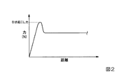
測定機器:[島津社製オートグラフ AGS-50NX]を用いて、剥離幅:25mm、ピール角:180°、ピール速度300mm/minで輝度向上フィルム21から表面保護フィルム22を剥離させるピール試験を行った。図2は、表面保護フィルム22を輝度向上フィルム21から引き起こす際の距離と力との関係を示す図である。図2に示されるように、表面保護フィルム22を輝度向上フィルム21から剥離させる際の初期段階では引き起こしに大きな力が必要であるが、剥離が始まった後は引き起こし力が小さくなる。本実施形態では、表面保護フィルム22が、始点から25mm剥がれる迄の間の最大値を引き起こし力とし、その後の力を剥離力とした。
・引き起こし力の上昇率 … UVB領域で積算光量が8000mJ/cm2となるように、照射強度が500mJ/cm2の活性エネルギー線を照射する前後で測定した引き起こし力を次の式を用いて上昇率を算出した。
上昇率=[(N1−N0)/N0]×100
単位:%、N0:UV照射前の引き起こし力、N1:UV照射後の引き起こし力
[Evaluation method]
(Causing force)
Measuring instrument: [Peel test for peeling the surface
· Causing force increase rate ... so that the accumulated amount of light in UVB region becomes 8000 mJ / cm 2, increasing the lead force irradiation intensity was measured before and after irradiation with active energy rays 500 mJ / cm 2 using the following formula The rate was calculated.
Rate of increase = [(N1-N0) / N0] x 100
Unit:%, N0: Cause force before UV irradiation, N1: Cause force after UV irradiation
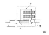
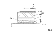
図3は、偏光板50における表面保護フィルム22を輝度向上フィルムから剥離するときの引き起こし力を測定する際の平面図である。図4は、表面保護フィルム22を輝度向上フィルムから剥離するときの引き起こし力を測定する際の断面図である。ピール試験においては、短冊状にカットした輝度向上フィルム21付き偏光板50の粘着剤層51を、図3および図4に示すように、ガラス70に貼合して行った。
FIG. 3 is a plan view when measuring the cause force when the surface
引き起こし力の測定は、10個のサンプルを用いて行い、その平均値を取った。引き起こし力の測定は、偏光板50への活性エネルギー線照射前と、活性エネルギー線照射後のそれぞれで実施した。活性エネルギー線照射後については、25℃、55%RHの環境下で放置しサンプルの温度が23℃まで冷めてから引き起こし力を測定した。
The measurement of the motive force was performed using 10 samples, and the average value was taken. The measurement of the causing force was performed before and after irradiation of the active energy ray to the
(輝度向上フィルム21の断面のアスペクト比)
測定機器:[オリンパス株式会社製 型番:OLS4100]を用いて、超高速モードで倍率を100倍として面粗さ測定を行った。輝度向上フィルムの延伸方向と垂直方向になる2つの端面から3cmずつ切り出し、幅5点ずつ測定した。アスペクト比が大きい程、断面には不均一な凹凸が存在し、荒れた状態である。アスペクト比が小さい程、断面は均一であり、クラックや欠陥が生じていないと考えられる。
(Aspect ratio of cross section of brightness enhancement film 21)
Using a measuring instrument: [Model number: OLS4100 manufactured by Olympus Corporation], the surface roughness was measured in an ultra high speed mode with a magnification of 100 times. 3 cm was cut out from each of two end faces perpendicular to the stretching direction of the brightness enhancement film, and the width was measured at 5 points. The larger the aspect ratio, the more uneven the surface is and the rougher the surface is. It is considered that the smaller the aspect ratio, the more uniform the cross section, and no cracks or defects are generated.
[サンプル作製]
図5に示す仕様に従い、実施例1〜3、比較例1〜2、参考例1〜5のサンプルを作製した。
[Sample preparation]
Samples of Examples 1 to 3, Comparative Examples 1 to 2, and Reference Examples 1 to 5 were produced according to the specifications shown in FIG.
[実施例1]
偏光板50は、次のように作製した。まず、厚さ60μmのポリビニルアルコールフィルム(平均重合度約2,400、ケン化度99.9モル%以上)を、乾式延伸により約5倍に一軸延伸し、さらに緊張状態を保ったまま、60℃の純水に1分間浸漬した後、ヨウ素/ヨウ化カリウム/水の重量比が 0.05/5/100の水溶液に28℃で60秒間浸漬した。その後、ヨウ化カリウム/ホウ酸/水の重量比が8.5/8.5/100の水溶液に72℃で300秒間浸漬した。引き続き26℃の純水で20秒間洗浄した後、65℃で乾燥し、ポリビニルアルコールフィルムにヨウ素が吸着配向している厚さ23μmの偏光子を得た。次に、この偏光子の片側に、水100部に対し、カルボキシル基変性ポリビニルアルコール〔株式会社クラレから入手した商品名“KL−318”〕を3部溶解し、その水溶液に水溶性エポキシ樹脂であるポリアミドエポキシ系添加剤〔田岡化学工業株式会社から入手した商品名“スミレーズレジン(登録商標) 650(30)”、固形分濃度30%の水溶液〕を 1.5部添加したエポキシ系接着剤を塗布し、透明の保護フィルム11として厚さ40μmのトリアセチルセルロースフィルム〔コニカミノルタオプト株式会社製の商品名“KC4UY”〕を貼り合せ、その反対側には前記の接着剤を用いて、厚みが26μmの輝度向上フィルム21(3M製、商品名 Advanced Polarized Film, Version 3)を貼合した。トリアセチルセルロースフィルム(保護フィルム11)を貼合した面に粘着剤を塗工して粘着剤層51を有する偏光板50を作製した。基材が厚み38μmの二軸延伸ポリエステルフィルムであり、粘着層が厚み15μmであって硬化剤と帯電防止剤を含む、表面保護フィルム22であるSAT4038T15−JSL(株式会社サンエー化研製)を、輝度向上フィルム21を貼合した面に前記粘着剤を介して貼合した。この表面保護フィルム22は、波長190nmの前記活性エネルギー線に対する透過率が5%以下であった。
[Example 1]
The
作製した輝度向上フィルム21付きの偏光板50を積層し、上記条件において端面研磨を実施した。この端面研磨後の輝度向上フィルム21の断面のアスペクト比はStr=0.30であった。このサンプルに対して積算光量が8000mJ/cm2の活性エネルギー線を照射した。表面保護フィルム22に、表面保護フィルム22を剥離するための接着シール71を貼り付けた後に、接着シール71の一方側(図3および図4の右側)の端部を他方側(図3および図4の左側)に引くことにより表面保護フィルム22を引き起こし、輝度向上フィルム21から剥離する際の引き起こし力を測定した。表面保護フィルム22を輝度向上フィルムから剥離するときの引き起こし力は4.8N/25mmであった。なお、活性化エネルギー線の照射前の引き起こし力は、0.77N/25mmであった。
The produced
[実施例2]
実施例1と同様の手順でサンプル作成し、同様の処理を施したが、APF-V3を保護する表面保護フィルム22には、基材が厚み38μmの二軸延伸ポリエステルフィルムであり、粘着層が厚み22μmであって、硬化剤と帯電防止剤を含む、SAT4538TF−JSL(株式会社サンエー化研製)を使用した。輝度向上フィルム21の断面のアスペクト比はStr=0.30であり、表面保護フィルム22を輝度向上フィルム21から剥離するときの引き起こし力は6.2N/25mmであった。この表面保護フィルム22は、波長190nmの前記活性エネルギー線に対する透過率が5%以下であった。
[Example 2]
Samples were prepared in the same procedure as in Example 1 and subjected to the same treatment, but the surface
[実施例3]
実施例1と同様の手順でサンプルを作成し、同様の処理を施したが、APF-V3を保護する表面保護フィルム22には、基材が厚み38μmの二軸延伸ポリエステルフィルムであり、粘着層が厚み22μmであって、硬化剤と帯電防止剤を含む、SAT4238TF−JSL(株式会社サンエー化研製)を使用した。輝度向上フィルムの断面のアスペクト比はStr=0.30であり、表面保護フィルム22を輝度向上フィルム21から剥離するときの引き起こし力は8.2N/25mmであった。この表面保護フィルム22は、波長190nmの前記活性エネルギー線に対する透過率が5%以下であった。
[Example 3]
A sample was prepared in the same procedure as in Example 1 and subjected to the same treatment, but the surface
[比較例1]
実施例1と同様の手順でサンプルを作成し、同様の処理を施したが、APF-V3を保護する表面保護フィルムには、基材が厚み38μmの二軸延伸ポリエステルフィルムであり、粘着層が厚み20μmであるAS3−304(藤森工業株式会社製)を図6に示した表面保護フィルム22として使用した。輝度向上フィルム21の断面のアスペクト比はStr=0.30であり、表面保護フィルムを輝度向上フィルム21から剥離するときの引き起こし力は12.0N/25mmであった。この表面保護フィルム22は、波長190nmの前記活性エネルギー線に対する透過率が5%以下であった。
[Comparative Example 1]
A sample was prepared in the same procedure as in Example 1 and subjected to the same treatment. However, the surface protective film for protecting APF-V3 was a biaxially stretched polyester film having a thickness of 38 μm, and an adhesive layer was formed. AS3-304 (made by Fujimori Kogyo Co., Ltd.) having a thickness of 20 μm was used as the surface
[比較例2]
実施例1と同様の手順でサンプルを作成し、同様の処理を施したが、APF-V3を保護する表面保護フィルムには、比較例1で用いた表面保護フィルム22Aと同様の構成であり、基材が厚み38μmの二軸延伸ポリエステルフィルムであり、粘着層が厚み15μmであるAS3−501(藤森工業株式会社製)を使用した。AS3−501はAS3−304と粘着剤の厚みと種類が異なる。輝度向上フィルムの断面のアスペクト比はStr=0.30であり、表面保護フィルムを輝度向上フィルム21から剥離するときの引き起こし力は大きすぎて、測定不可であった。この表面保護フィルム22は、波長190nmの前記活性エネルギー線に対する透過率が5%以下であった。
[Comparative Example 2]
Samples were prepared in the same procedure as in Example 1 and subjected to the same treatment, but the surface protective film for protecting APF-V3 has the same configuration as the surface protective film 22A used in Comparative Example 1, AS3-501 (made by Fujimori Kogyo Co., Ltd.) having a base material of a biaxially stretched polyester film having a thickness of 38 μm and an adhesive layer having a thickness of 15 μm was used. AS3-501 differs from AS3-304 in the thickness and type of adhesive. The cross-sectional aspect ratio of the brightness enhancement film was Str = 0.30, and the cause force when peeling the surface protective film from the
[参考例1]
実施例1と同様の手順でサンプルを作成し、同様の処理を施したが、活性エネルギー線は照射しなかった。端面研磨後の輝度向上フィルム21の断面のアスペクト比はStr=0.30であった。短冊状にカットした輝度向上フィルム21付き偏光板50の粘着剤層51をガラス70に貼合した。表面保護フィルム22を輝度向上フィルム21から剥離するときの引き起こし力は0.77N/25mmであった。
[Reference Example 1]
Samples were prepared and processed in the same procedure as in Example 1, but the active energy rays were not irradiated. The aspect ratio of the cross section of the
[参考例2]
実施例2と同様の手順でサンプルを作成し、同様の処理を施したが、活性エネルギー線は照射しなかった。端面研磨後の輝度向上フィルム21の断面のアスペクト比はStr=0.30であった。短冊状にカットした輝度向上フィルム21付き偏光板50の粘着剤層51をガラス70に貼合した。表面保護フィルム22を輝度向上フィルム21から剥離するときの引き起こし力は2.6N/25mmであった。
[Reference Example 2]
Samples were prepared and processed in the same procedure as in Example 2, but the active energy rays were not irradiated. The aspect ratio of the cross section of the
[参考例3]
実施例3と同様の手順でサンプルを作成し、同様の処理を施したが、活性エネルギー線は照射しなかった。端面研磨後の輝度向上フィルム21の断面のアスペクト比はStr=0.30であった。短冊状にカットした輝度向上フィルム21付き偏光板50の粘着剤層51をガラス70に貼合した。表面保護フィルム22を輝度向上フィルム21から剥離するときの引き起こし力は1.4N/25mmであった。
[Reference Example 3]
A sample was prepared in the same procedure as in Example 3 and subjected to the same treatment, but the active energy ray was not irradiated. The aspect ratio of the cross section of the
[参考例4]
比較例1と同様の手順でサンプルを作成し、同様の処理を施したが、活性エネルギー線は照射しなかった。端面研磨後の輝度向上フィルム21の断面のアスペクト比はStr=0.30であった。短冊状にカットした輝度向上フィルム21付き偏光板50の粘着剤層51をガラス70に貼合した。表面保護フィルム22を輝度向上フィルム21から剥離するときの引き起こし力は1.2N/25mmであった。
[Reference Example 4]
Samples were prepared and processed in the same procedure as in Comparative Example 1, but the active energy rays were not irradiated. The aspect ratio of the cross section of the
[参考例5]
比較例2と同様の手順でサンプルを作成し、同様の処理を施したが、活性エネルギー線は照射しなかった。端面研磨後の輝度向上フィルム21の断面のアスペクト比はStr=0.30であった。短冊状にカットした輝度向上フィルム21付き偏光板50の粘着剤層51をガラス70に貼合した。表面保護フィルム22を輝度向上フィルム21から剥離するときの引き起こし力は7.0N/25mmであった。
[Reference Example 5]
A sample was prepared and processed in the same procedure as in Comparative Example 2, but the active energy ray was not irradiated. The aspect ratio of the cross section of the
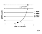
図7は、上記の引き起こし力と、輝度向上フィルム21における層間剥離発生率との関係を示す図である。図7に示されるように、引き起こし力が大きいほど層間剥離発生率が大きくなることが確認できた。本実施形態では、図5に示されるように、層間剥離発生率が0〜10%以下の場合を○、10%を超え20%以下の場合を△、20%を超えた場合を×の評価とした。
FIG. 7 is a diagram showing the relationship between the above-mentioned cause force and the delamination occurrence rate in the
一方、活性エネルギー線照射を実施した場合であって、引き起こし力が10.0N/25mmを超えた場合、あるいは引き起こし力の上昇率が700%以上の場合に層間剥離発生率が×の結果となったが、引き起こし力が10.0N/25mm以下であり、引き起こし力の上昇率が700%未満であれば層間剥離発生率が○または△で良好な結果であることが確認できた。 On the other hand, when active energy ray irradiation is performed and the cause force exceeds 10.0 N / 25 mm, or when the increase rate of the cause force is 700% or more, the delamination occurrence rate is a result of x. However, if the cause force was 10.0 N / 25 mm or less and the rate of increase of the cause force was less than 700%, it was confirmed that the delamination occurrence rate was good or good with a good result.
以上、添付図面を参照しながら本発明に係る好適な実施形態について説明したが、本発明は係る例に限定されないことは言うまでもない。上述した例において示した各構成部材の諸形状や組み合わせ等は一例であって、本発明の主旨から逸脱しない範囲において設計要求等に基づき種々変更可能である。 The preferred embodiments according to the present invention have been described above with reference to the accompanying drawings, but the present invention is not limited to the examples. Various shapes, combinations, and the like of the constituent members shown in the above-described examples are examples, and various modifications can be made based on design requirements and the like without departing from the gist of the present invention.
10…偏光フィルム(吸収型偏光フィルム)、 20…光学フィルム、 21…輝度向上フィルム、 22…表面保護フィルム、 50…偏光板
DESCRIPTION OF
Claims (3)
積算光量が8000mJ/cm2の活性エネルギー線が照射された後に、前記表面保護フィルムを前記輝度向上フィルムから剥離するときに要する引き起こし力が10.0N/25mm以下であり、
前記引き起こし力の上昇率が700%未満である光学フィルム。 An optical film comprising a surface protective film and a brightness enhancement film,
After the active energy ray having an accumulated light amount of 8000 mJ / cm 2 is irradiated, the cause force required for peeling the surface protective film from the brightness enhancement film is 10.0 N / 25 mm or less,
An optical film having an increase rate of the inducing force of less than 700%.
Priority Applications (4)
| Application Number | Priority Date | Filing Date | Title |
|---|---|---|---|
| JP2016064593A JP2017181597A (en) | 2016-03-28 | 2016-03-28 | Optical film and polarizing plate |
| TW106109165A TWI813536B (en) | 2016-03-28 | 2017-03-20 | Optical film and polarizing plate |
| KR1020170035873A KR102294328B1 (en) | 2016-03-28 | 2017-03-22 | Optical film and polarizing plate |
| CN201710176196.3A CN107238876B (en) | 2016-03-28 | 2017-03-22 | Optical film and polarizing plate |
Applications Claiming Priority (1)
| Application Number | Priority Date | Filing Date | Title |
|---|---|---|---|
| JP2016064593A JP2017181597A (en) | 2016-03-28 | 2016-03-28 | Optical film and polarizing plate |
Related Child Applications (1)
| Application Number | Title | Priority Date | Filing Date |
|---|---|---|---|
| JP2018085774A Division JP2018151648A (en) | 2018-04-26 | 2018-04-26 | Optical film and polarizing plate |
Publications (1)
| Publication Number | Publication Date |
|---|---|
| JP2017181597A true JP2017181597A (en) | 2017-10-05 |
Family
ID=59983760
Family Applications (1)
| Application Number | Title | Priority Date | Filing Date |
|---|---|---|---|
| JP2016064593A Pending JP2017181597A (en) | 2016-03-28 | 2016-03-28 | Optical film and polarizing plate |
Country Status (4)
| Country | Link |
|---|---|
| JP (1) | JP2017181597A (en) |
| KR (1) | KR102294328B1 (en) |
| CN (1) | CN107238876B (en) |
| TW (1) | TWI813536B (en) |
Cited By (3)
| Publication number | Priority date | Publication date | Assignee | Title |
|---|---|---|---|---|
| JP2020095287A (en) * | 2017-10-31 | 2020-06-18 | 住友化学株式会社 | Laminate body |
| JP2021047453A (en) * | 2019-03-14 | 2021-03-25 | 住友化学株式会社 | Polarizer |
| WO2021205727A1 (en) * | 2020-04-09 | 2021-10-14 | 住友化学株式会社 | Optical laminate and peeling method |
Citations (3)
| Publication number | Priority date | Publication date | Assignee | Title |
|---|---|---|---|---|
| JPH0860111A (en) * | 1994-08-23 | 1996-03-05 | Sekisui Chem Co Ltd | Surface-protective film |
| JP2004258393A (en) * | 2003-02-26 | 2004-09-16 | Sumitomo Chem Co Ltd | Interlayer exfoliation preventing method of film |
| JP2010277063A (en) * | 2009-04-27 | 2010-12-09 | Sumitomo Chemical Co Ltd | Liquid crystal display device |
Family Cites Families (11)
| Publication number | Priority date | Publication date | Assignee | Title |
|---|---|---|---|---|
| JPH06145616A (en) * | 1992-11-10 | 1994-05-27 | Sekisui Chem Co Ltd | Surface-protection film |
| JP2000347181A (en) | 1999-06-09 | 2000-12-15 | Nitto Denko Corp | Optical member and liquid crystal display device |
| JP2010054824A (en) * | 2008-08-28 | 2010-03-11 | Sumitomo Chemical Co Ltd | Polarizing plate and method of manufacturing the same |
| JP5147014B2 (en) * | 2008-10-08 | 2013-02-20 | 住友化学株式会社 | High contrast polarizing plate and liquid crystal display device |
| JP5335401B2 (en) | 2008-12-19 | 2013-11-06 | 富士フイルム株式会社 | Polarizing film, polarizing film manufacturing method, polarizing plate, polarizing plate manufacturing method, and anti-reflection film for vehicle |
| JP4982533B2 (en) | 2009-07-30 | 2012-07-25 | 富士フイルム株式会社 | Manufacturing method of polarizing plate |
| TWI592305B (en) * | 2010-11-10 | 2017-07-21 | Sumitomo Chemical Co | Polarizing film and polarizing plate manufacturing method |
| JP2014189786A (en) * | 2013-03-28 | 2014-10-06 | Nitto Denko Corp | Adhesive composition, adhesive sheet and optical film |
| JP6664866B2 (en) * | 2013-04-05 | 2020-03-13 | 住友化学株式会社 | Set of polarizing plate and front panel integrated liquid crystal display panel |
| JP6289104B2 (en) | 2014-01-08 | 2018-03-07 | 日東電工株式会社 | Film adhesive, dicing tape with film adhesive, semiconductor device manufacturing method, and semiconductor device |
| KR101912159B1 (en) * | 2014-06-27 | 2018-10-26 | 후지필름 가부시키가이샤 | Method of manufacturing transfer material of luminance-improving film |
-
2016
- 2016-03-28 JP JP2016064593A patent/JP2017181597A/en active Pending
-
2017
- 2017-03-20 TW TW106109165A patent/TWI813536B/en active
- 2017-03-22 CN CN201710176196.3A patent/CN107238876B/en active Active
- 2017-03-22 KR KR1020170035873A patent/KR102294328B1/en active IP Right Grant
Patent Citations (3)
| Publication number | Priority date | Publication date | Assignee | Title |
|---|---|---|---|---|
| JPH0860111A (en) * | 1994-08-23 | 1996-03-05 | Sekisui Chem Co Ltd | Surface-protective film |
| JP2004258393A (en) * | 2003-02-26 | 2004-09-16 | Sumitomo Chem Co Ltd | Interlayer exfoliation preventing method of film |
| JP2010277063A (en) * | 2009-04-27 | 2010-12-09 | Sumitomo Chemical Co Ltd | Liquid crystal display device |
Cited By (4)
| Publication number | Priority date | Publication date | Assignee | Title |
|---|---|---|---|---|
| JP2020095287A (en) * | 2017-10-31 | 2020-06-18 | 住友化学株式会社 | Laminate body |
| JP2021047453A (en) * | 2019-03-14 | 2021-03-25 | 住友化学株式会社 | Polarizer |
| JP7284141B2 (en) | 2019-03-14 | 2023-05-30 | 住友化学株式会社 | Polarizer |
| WO2021205727A1 (en) * | 2020-04-09 | 2021-10-14 | 住友化学株式会社 | Optical laminate and peeling method |
Also Published As
| Publication number | Publication date |
|---|---|
| TWI813536B (en) | 2023-09-01 |
| KR102294328B1 (en) | 2021-08-25 |
| CN107238876B (en) | 2020-05-05 |
| CN107238876A (en) | 2017-10-10 |
| KR20170113168A (en) | 2017-10-12 |
| TW201741699A (en) | 2017-12-01 |
Similar Documents
| Publication | Publication Date | Title |
|---|---|---|
| JP5082480B2 (en) | Thin polarizing plate and image display device using the same | |
| JP6862662B2 (en) | Polarizing plate, polarizing plate with adhesive, and liquid crystal display device | |
| JP2019109329A (en) | Laminated body | |
| JP2010277018A (en) | Polarizing plate excellent in durability, method of manufacturing the same, and image display device using the same | |
| JP2011022202A (en) | Polarizing plate and image display device using the same | |
| KR101757062B1 (en) | Polarizing plate and liquid crystal display device | |
| JP2016118761A (en) | Polarizing plate and manufacturing method of the same, and set of polarizing plates, liquid crystal panel, and liquid crystal display device | |
| JP6680347B2 (en) | Laminate | |
| KR101969636B1 (en) | Polarizing plate set and liquid crystal panel | |
| TWI791058B (en) | Laminate | |
| JP2008197310A (en) | Thin polarizing plate, composite polarizing plate, image display device, and method for manufacturing composite polarizing plate | |
| TWI715793B (en) | Polarizing plate set, liquid crystal display panel and liquid crystal display device | |
| KR102294328B1 (en) | Optical film and polarizing plate | |
| JP5878746B2 (en) | Composite polarizing plate set, liquid crystal panel and liquid crystal display device | |
| JP2017156399A (en) | Set of polarizing plates and liquid crystal panel | |
| JP2023001208A (en) | optical sheet | |
| JP2018151648A (en) | Optical film and polarizing plate | |
| KR20100023749A (en) | Polarizing plate | |
| JP2014191205A (en) | Production method of laminate optical film | |
| JP2012159624A (en) | Composite polarizing plate set, liquid crystal panel and liquid crystal display device | |
| WO2014175462A1 (en) | Method for manufacturing polarizing plate | |
| JP2018067020A (en) | Set of polarizing plates and liquid crystal panel |
Legal Events
| Date | Code | Title | Description |
|---|---|---|---|
| A131 | Notification of reasons for refusal |
Free format text: JAPANESE INTERMEDIATE CODE: A131 Effective date: 20170808 |
|
| A02 | Decision of refusal |
Free format text: JAPANESE INTERMEDIATE CODE: A02 Effective date: 20180130 |