JP2017167478A - Liquid crystal display device and mother substrate for the same - Google Patents
Liquid crystal display device and mother substrate for the same Download PDFInfo
- Publication number
- JP2017167478A JP2017167478A JP2016055280A JP2016055280A JP2017167478A JP 2017167478 A JP2017167478 A JP 2017167478A JP 2016055280 A JP2016055280 A JP 2016055280A JP 2016055280 A JP2016055280 A JP 2016055280A JP 2017167478 A JP2017167478 A JP 2017167478A
- Authority
- JP
- Japan
- Prior art keywords
- organic passivation
- passivation film
- liquid crystal
- crystal display
- display device
- Prior art date
- Legal status (The legal status is an assumption and is not a legal conclusion. Google has not performed a legal analysis and makes no representation as to the accuracy of the status listed.)
- Pending
Links
Images


Classifications
-
- G—PHYSICS
- G02—OPTICS
- G02F—OPTICAL DEVICES OR ARRANGEMENTS FOR THE CONTROL OF LIGHT BY MODIFICATION OF THE OPTICAL PROPERTIES OF THE MEDIA OF THE ELEMENTS INVOLVED THEREIN; NON-LINEAR OPTICS; FREQUENCY-CHANGING OF LIGHT; OPTICAL LOGIC ELEMENTS; OPTICAL ANALOGUE/DIGITAL CONVERTERS
- G02F1/00—Devices or arrangements for the control of the intensity, colour, phase, polarisation or direction of light arriving from an independent light source, e.g. switching, gating or modulating; Non-linear optics
- G02F1/01—Devices or arrangements for the control of the intensity, colour, phase, polarisation or direction of light arriving from an independent light source, e.g. switching, gating or modulating; Non-linear optics for the control of the intensity, phase, polarisation or colour
- G02F1/13—Devices or arrangements for the control of the intensity, colour, phase, polarisation or direction of light arriving from an independent light source, e.g. switching, gating or modulating; Non-linear optics for the control of the intensity, phase, polarisation or colour based on liquid crystals, e.g. single liquid crystal display cells
- G02F1/133—Constructional arrangements; Operation of liquid crystal cells; Circuit arrangements
- G02F1/1333—Constructional arrangements; Manufacturing methods
- G02F1/1339—Gaskets; Spacers; Sealing of cells
-
- G—PHYSICS
- G02—OPTICS
- G02F—OPTICAL DEVICES OR ARRANGEMENTS FOR THE CONTROL OF LIGHT BY MODIFICATION OF THE OPTICAL PROPERTIES OF THE MEDIA OF THE ELEMENTS INVOLVED THEREIN; NON-LINEAR OPTICS; FREQUENCY-CHANGING OF LIGHT; OPTICAL LOGIC ELEMENTS; OPTICAL ANALOGUE/DIGITAL CONVERTERS
- G02F1/00—Devices or arrangements for the control of the intensity, colour, phase, polarisation or direction of light arriving from an independent light source, e.g. switching, gating or modulating; Non-linear optics
- G02F1/01—Devices or arrangements for the control of the intensity, colour, phase, polarisation or direction of light arriving from an independent light source, e.g. switching, gating or modulating; Non-linear optics for the control of the intensity, phase, polarisation or colour
- G02F1/13—Devices or arrangements for the control of the intensity, colour, phase, polarisation or direction of light arriving from an independent light source, e.g. switching, gating or modulating; Non-linear optics for the control of the intensity, phase, polarisation or colour based on liquid crystals, e.g. single liquid crystal display cells
- G02F1/133—Constructional arrangements; Operation of liquid crystal cells; Circuit arrangements
- G02F1/1333—Constructional arrangements; Manufacturing methods
- G02F1/133345—Insulating layers
-
- G—PHYSICS
- G02—OPTICS
- G02F—OPTICAL DEVICES OR ARRANGEMENTS FOR THE CONTROL OF LIGHT BY MODIFICATION OF THE OPTICAL PROPERTIES OF THE MEDIA OF THE ELEMENTS INVOLVED THEREIN; NON-LINEAR OPTICS; FREQUENCY-CHANGING OF LIGHT; OPTICAL LOGIC ELEMENTS; OPTICAL ANALOGUE/DIGITAL CONVERTERS
- G02F1/00—Devices or arrangements for the control of the intensity, colour, phase, polarisation or direction of light arriving from an independent light source, e.g. switching, gating or modulating; Non-linear optics
- G02F1/01—Devices or arrangements for the control of the intensity, colour, phase, polarisation or direction of light arriving from an independent light source, e.g. switching, gating or modulating; Non-linear optics for the control of the intensity, phase, polarisation or colour
- G02F1/13—Devices or arrangements for the control of the intensity, colour, phase, polarisation or direction of light arriving from an independent light source, e.g. switching, gating or modulating; Non-linear optics for the control of the intensity, phase, polarisation or colour based on liquid crystals, e.g. single liquid crystal display cells
- G02F1/133—Constructional arrangements; Operation of liquid crystal cells; Circuit arrangements
- G02F1/1333—Constructional arrangements; Manufacturing methods
- G02F1/133351—Manufacturing of individual cells out of a plurality of cells, e.g. by dicing
-
- G—PHYSICS
- G02—OPTICS
- G02F—OPTICAL DEVICES OR ARRANGEMENTS FOR THE CONTROL OF LIGHT BY MODIFICATION OF THE OPTICAL PROPERTIES OF THE MEDIA OF THE ELEMENTS INVOLVED THEREIN; NON-LINEAR OPTICS; FREQUENCY-CHANGING OF LIGHT; OPTICAL LOGIC ELEMENTS; OPTICAL ANALOGUE/DIGITAL CONVERTERS
- G02F1/00—Devices or arrangements for the control of the intensity, colour, phase, polarisation or direction of light arriving from an independent light source, e.g. switching, gating or modulating; Non-linear optics
- G02F1/01—Devices or arrangements for the control of the intensity, colour, phase, polarisation or direction of light arriving from an independent light source, e.g. switching, gating or modulating; Non-linear optics for the control of the intensity, phase, polarisation or colour
- G02F1/13—Devices or arrangements for the control of the intensity, colour, phase, polarisation or direction of light arriving from an independent light source, e.g. switching, gating or modulating; Non-linear optics for the control of the intensity, phase, polarisation or colour based on liquid crystals, e.g. single liquid crystal display cells
- G02F1/133—Constructional arrangements; Operation of liquid crystal cells; Circuit arrangements
- G02F1/1333—Constructional arrangements; Manufacturing methods
- G02F1/1335—Structural association of cells with optical devices, e.g. polarisers or reflectors
- G02F1/133509—Filters, e.g. light shielding masks
- G02F1/133514—Colour filters
-
- G—PHYSICS
- G02—OPTICS
- G02F—OPTICAL DEVICES OR ARRANGEMENTS FOR THE CONTROL OF LIGHT BY MODIFICATION OF THE OPTICAL PROPERTIES OF THE MEDIA OF THE ELEMENTS INVOLVED THEREIN; NON-LINEAR OPTICS; FREQUENCY-CHANGING OF LIGHT; OPTICAL LOGIC ELEMENTS; OPTICAL ANALOGUE/DIGITAL CONVERTERS
- G02F1/00—Devices or arrangements for the control of the intensity, colour, phase, polarisation or direction of light arriving from an independent light source, e.g. switching, gating or modulating; Non-linear optics
- G02F1/01—Devices or arrangements for the control of the intensity, colour, phase, polarisation or direction of light arriving from an independent light source, e.g. switching, gating or modulating; Non-linear optics for the control of the intensity, phase, polarisation or colour
- G02F1/13—Devices or arrangements for the control of the intensity, colour, phase, polarisation or direction of light arriving from an independent light source, e.g. switching, gating or modulating; Non-linear optics for the control of the intensity, phase, polarisation or colour based on liquid crystals, e.g. single liquid crystal display cells
- G02F1/133—Constructional arrangements; Operation of liquid crystal cells; Circuit arrangements
- G02F1/1333—Constructional arrangements; Manufacturing methods
- G02F1/1339—Gaskets; Spacers; Sealing of cells
- G02F1/13394—Gaskets; Spacers; Sealing of cells spacers regularly patterned on the cell subtrate, e.g. walls, pillars
-
- G—PHYSICS
- G02—OPTICS
- G02F—OPTICAL DEVICES OR ARRANGEMENTS FOR THE CONTROL OF LIGHT BY MODIFICATION OF THE OPTICAL PROPERTIES OF THE MEDIA OF THE ELEMENTS INVOLVED THEREIN; NON-LINEAR OPTICS; FREQUENCY-CHANGING OF LIGHT; OPTICAL LOGIC ELEMENTS; OPTICAL ANALOGUE/DIGITAL CONVERTERS
- G02F1/00—Devices or arrangements for the control of the intensity, colour, phase, polarisation or direction of light arriving from an independent light source, e.g. switching, gating or modulating; Non-linear optics
- G02F1/01—Devices or arrangements for the control of the intensity, colour, phase, polarisation or direction of light arriving from an independent light source, e.g. switching, gating or modulating; Non-linear optics for the control of the intensity, phase, polarisation or colour
- G02F1/13—Devices or arrangements for the control of the intensity, colour, phase, polarisation or direction of light arriving from an independent light source, e.g. switching, gating or modulating; Non-linear optics for the control of the intensity, phase, polarisation or colour based on liquid crystals, e.g. single liquid crystal display cells
- G02F1/133—Constructional arrangements; Operation of liquid crystal cells; Circuit arrangements
- G02F1/1333—Constructional arrangements; Manufacturing methods
- G02F1/1345—Conductors connecting electrodes to cell terminals
- G02F1/13458—Terminal pads
-
- G—PHYSICS
- G02—OPTICS
- G02F—OPTICAL DEVICES OR ARRANGEMENTS FOR THE CONTROL OF LIGHT BY MODIFICATION OF THE OPTICAL PROPERTIES OF THE MEDIA OF THE ELEMENTS INVOLVED THEREIN; NON-LINEAR OPTICS; FREQUENCY-CHANGING OF LIGHT; OPTICAL LOGIC ELEMENTS; OPTICAL ANALOGUE/DIGITAL CONVERTERS
- G02F1/00—Devices or arrangements for the control of the intensity, colour, phase, polarisation or direction of light arriving from an independent light source, e.g. switching, gating or modulating; Non-linear optics
- G02F1/01—Devices or arrangements for the control of the intensity, colour, phase, polarisation or direction of light arriving from an independent light source, e.g. switching, gating or modulating; Non-linear optics for the control of the intensity, phase, polarisation or colour
- G02F1/13—Devices or arrangements for the control of the intensity, colour, phase, polarisation or direction of light arriving from an independent light source, e.g. switching, gating or modulating; Non-linear optics for the control of the intensity, phase, polarisation or colour based on liquid crystals, e.g. single liquid crystal display cells
- G02F1/133—Constructional arrangements; Operation of liquid crystal cells; Circuit arrangements
- G02F1/136—Liquid crystal cells structurally associated with a semi-conducting layer or substrate, e.g. cells forming part of an integrated circuit
- G02F1/1362—Active matrix addressed cells
- G02F1/1368—Active matrix addressed cells in which the switching element is a three-electrode device
Landscapes
- Physics & Mathematics (AREA)
- Nonlinear Science (AREA)
- Mathematical Physics (AREA)
- Chemical & Material Sciences (AREA)
- Crystallography & Structural Chemistry (AREA)
- General Physics & Mathematics (AREA)
- Optics & Photonics (AREA)
- Engineering & Computer Science (AREA)
- Manufacturing & Machinery (AREA)
- Microelectronics & Electronic Packaging (AREA)
- Liquid Crystal (AREA)
Abstract
【課題】マザー基板から取り出すことができる液晶表示パネルの数を増やす。【解決手段】TFT基板100と対向基板200が前記対向基板200の周辺に形成されたシール部において接着し、前記TFT基板100において前記対向基板が対向していない部分に端子部が形成された液晶表示装置であって、前記TFT基板100には、前記端子部の端部に沿って土手状の有機パッシベーション膜102が形成され、前記有機パッシベーション膜102には段部1023が形成され、前記有機パッシベーション膜102の前記段部1023より前記端部側における膜厚は、前記段部より内側の膜厚よりも大きいことを特徴とする液晶表示装置。【選択図】図9An object of the present invention is to increase the number of liquid crystal display panels that can be taken out from a mother board. A liquid crystal display in which a TFT substrate (100) and a counter substrate (200) are bonded together at a sealing portion formed around the counter substrate (200), and a terminal portion is formed in a portion of the TFT substrate (100) not opposed to the counter substrate. In the display device, a bank-shaped organic passivation film 102 is formed on the TFT substrate 100 along the edge of the terminal portion, a stepped portion 1023 is formed on the organic passivation film 102, and the organic passivation A liquid crystal display device, wherein the film thickness of the film 102 on the side of the end portion from the stepped portion 1023 is larger than the film thickness on the inner side of the stepped portion. [Selection drawing] Fig. 9
Description
本発明は表示装置に係り、特に、液晶表示パネルをマザー基板から多く取得できる技術に関する。 The present invention relates to a display device, and more particularly to a technique capable of acquiring a large number of liquid crystal display panels from a mother substrate.
液晶表示装置では画素電極および薄膜トランジスタ(TFT)等を有する画素がマトリクス状に形成されたTFT基板と、TFT基板に対向して対向基板が配置され、TFT基板と対向基板の間に液晶が挟持されている構成となっている。そして液晶分子による光の透過率を画素毎に制御することによって画像を形成している。 In a liquid crystal display device, a TFT substrate in which pixels having pixel electrodes and thin film transistors (TFTs) are formed in a matrix and a counter substrate are arranged opposite the TFT substrate, and liquid crystal is sandwiched between the TFT substrate and the counter substrate. It has become the composition. An image is formed by controlling the light transmittance of the liquid crystal molecules for each pixel.
液晶表示パネルは、1個ずつ形成したのでは効率が悪いので、マザー基板に多数の液晶表示パネルを形成し、マザー基板が完成した後、個々の液晶表示パネルをマザー基板から分離して取り出すことが行われている。液晶表示パネルをマザー基板から分離する際、分離線に沿ってスクライビングを行い、衝撃を加えて個々の液晶表示パネルを分離する。 Since it is inefficient to form each liquid crystal display panel one by one, a large number of liquid crystal display panels are formed on the mother substrate, and after the mother substrate is completed, the individual liquid crystal display panels are separated from the mother substrate and taken out. Has been done. When the liquid crystal display panel is separated from the mother substrate, scribing is performed along the separation line, and an impact is applied to separate the individual liquid crystal display panels.
特許文献1には、マザー基板から、個々の液晶表示パネルを分離する技術が記載されている。
1枚のマザー基板から多数の液晶表示パネルを得ることができれば、液晶表示パネルの製造コストの低減になる。マザー基板が出来るだけ多数の液晶表示パネルを取り出すためには、マザー基板における液晶表示パネル間に間隔を設けないことが理想である。 If a large number of liquid crystal display panels can be obtained from one mother substrate, the manufacturing cost of the liquid crystal display panel can be reduced. In order for the mother substrate to take out as many liquid crystal display panels as possible, it is ideal that no space be provided between the liquid crystal display panels in the mother substrate.
一方、液晶表示装置は、外形をある値に抑えたまま、表示領域を大きくしたいという要求が強い。この要求に応えるためには、額縁の幅を小さくするとともに、端子部の面積を小さくする必要ある。端子部には、液晶表示パネルに電力や信号を供給するための端子が形成されている。マザー基板の状態において、隣接する液晶表示パネルからシール材や配向膜がこの端子部にはみ出してくると、端子の接続不良をきたす。 On the other hand, there is a strong demand for a liquid crystal display device to increase the display area while keeping the outer shape at a certain value. In order to meet this requirement, it is necessary to reduce the width of the frame and the area of the terminal portion. In the terminal portion, terminals for supplying power and signals to the liquid crystal display panel are formed. In the state of the mother substrate, if the sealing material or the alignment film protrudes from the adjacent liquid crystal display panel to the terminal portion, poor connection of the terminal is caused.
また、画面が高精細になるにしたがって、端子のピッチが小さくなる。端子には、端子金属を覆ってITO(Indium Tin Oxide)が形成されている。ITOはフォトリソグラフィによってパターニングされるが、ITOの残渣が存在すると、端子間のショートの問題が生ずる。 Also, as the screen becomes higher definition, the terminal pitch becomes smaller. The terminal is formed with ITO (Indium Tin Oxide) covering the terminal metal. ITO is patterned by photolithography, but if there is an ITO residue, a problem of short circuit between terminals occurs.
本発明の課題は、以上のような問題点を解決し、液晶表示装置の信頼性を維持しながら、マザー基板から多数の液晶表示パネルを取得することを可能にすることである。 An object of the present invention is to solve the above-described problems and to obtain a large number of liquid crystal display panels from a mother substrate while maintaining the reliability of the liquid crystal display device.
本発明は上記問題を克服するものであり、具体的な主な手段は次のとおりである。 The present invention overcomes the above-described problems, and specific main means are as follows.
(1)TFT基板と対向基板が前記対向基板の周辺に形成されたシール部において接着し、前記TFT基板において前記対向基板が対向していない部分に端子部が形成された液晶表示装置であって、前記TFT基板には、前記端子部の端部に沿って土手状の有機パッシベーション膜が形成され、
前記有機パッシベーション膜には段部が形成され、前記有機パッシベーション膜の前記段部より前記端部側における膜厚は、前記段部より内側の膜厚よりも大きいことを特徴とする液晶表示装置。
(1) A liquid crystal display device in which a TFT substrate and a counter substrate are bonded together at a seal portion formed around the counter substrate, and a terminal portion is formed in a portion of the TFT substrate where the counter substrate is not opposed. The TFT substrate is formed with a bank-like organic passivation film along the end of the terminal portion.
A step portion is formed in the organic passivation film, and a film thickness of the organic passivation film on the end portion side from the step portion is larger than a film thickness inside the step portion.
(2)有機パッシベーション膜を有するTFT基板と対向基板が前記対向基板の周辺に形成されたシール部において接着し、前記TFT基板において前記対向基板が対向していない部分に端子部が形成され、前記シール部に囲まれた領域に表示領域が形成された液晶表示装置であって、前記端子部の反対側の辺の前記シール部おいて、前記対向基板には、前記辺に沿って土手状スペーサが形成され、前記土手状スペーサは、前記辺の端部に沿って第1の膜厚を有する第1の部分と、前記第1の部分よりも内側に前記第1の膜厚よりも大きい第2の膜厚を有する第2の部分を有し、前記TFT基板には前記土手状スペーサに対応する位置に第1の土手状有機パッシベーション膜が形成され、前記第1の土手状有機パッシベーション膜の先端は、前記土手状スペーサの前記第1の部分と対向していることを特徴とする液晶表示装置。 (2) A TFT substrate having an organic passivation film and a counter substrate are bonded to each other at a seal portion formed around the counter substrate, and a terminal portion is formed in a portion of the TFT substrate where the counter substrate does not face, A liquid crystal display device in which a display region is formed in a region surrounded by a seal portion, wherein the counter substrate has a bank-like spacer along the side in the seal portion on the side opposite to the terminal portion. The bank-shaped spacer includes a first portion having a first film thickness along an end of the side, and a first film having a thickness greater than the first film thickness inside the first portion. A first bank-like organic passivation film is formed on the TFT substrate at a position corresponding to the bank-like spacer, and the first bank-like organic passivation film is formed on the TFT substrate. The tip is The liquid crystal display device, characterized in that opposite to the first portion of the serial bank-shaped spacer.
以下に実施例を用いて本発明の内容を詳細に説明する。 The contents of the present invention will be described in detail below using examples.
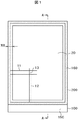
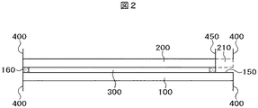
図1は本発明が適用される液晶表示パネルの例を示す平面図であり、図2は、図1のA−A部分の断面図である。図1の液晶表示パネルは、例えば、携帯電話等に使用される液晶表示装置に使用される。図1および図2において、TFT基板100と対向基板200がシール材160によって接着し、TFT基板100と対向基板200の間に液晶300が挟持されている。TFT基板100は対向基板200よりも大きく形成され、TFT基板100が対向基板200と重畳していない部分は端子部150となっている。
FIG. 1 is a plan view showing an example of a liquid crystal display panel to which the present invention is applied, and FIG. 2 is a cross-sectional view taken along line AA of FIG. The liquid crystal display panel of FIG. 1 is used, for example, in a liquid crystal display device used for a mobile phone or the like. In FIG. 1 and FIG. 2, the
図1において、表示領域20の外側が額縁領域になっており、額縁領域にシール材160が形成されている。図1に示すような液晶表示装置では、表示領域20を出来るだけ大きくすることが要求されており、その結果、額縁領域の幅waは1mm以下あるいは、0.7mm以下となっている。
In FIG. 1, the outside of the
表示領域20では、走査線11が第1の方向に延在し、第2の方向に配列している。また、映像信号線12が第2の方向に延在し、第1の方向に配列している。走査線11と映像信号線12で囲まれた領域が画素13となっている。高精細の表示装置では、画素13が小さくなり、映像信号線12のピッチは、30μm以下である場合も存在する。
In the
図1において、TFT基板100が対向基板200と重畳していない部分である端子部150には、液晶表示パネルに電力や信号を供給するフレキシブル配線基板を接続するための端子が形成されている。また、走査線11や映像信号線12を駆動するためのドライバICがCOG(Chip On Glass)等によって接続されるが、このための端子も形成されている。
In FIG. 1, terminals for connecting a flexible wiring substrate for supplying power and signals to the liquid crystal display panel are formed in a
図2において、TFT基板100と対向基板200がシール材160によって接着し、内部に液晶300が封入されている。TFT基板100の端子部150の上からは、対向基板200を除去する必要があるので、分離線450において、対向基板200の端材210を除去する。端材210を除去する方法は、分離線450の部分にスクライビングを入れ、衝撃を加えて、除去する。一方、液晶表示パネルは、分離線400において、TFT基板100側と対向基板200にスクライビングを入れ、衝撃を加えることによってマザー基板から分離される。
図3は、従来例によるマザー基板における液晶表示パネルの配置例である。以後、マザー基板から分離されていない状態の個々の液晶表示パネルを液晶セルと呼ぶこともある。図3において、表示領域を囲んで、ディスペンサ等によってシール材160が塗布される。端子部150側では、シール材160が2本形成されている。また、端子部150と反対側の短辺側には、分離線400を挟んでダミーのシール材が形成されている。スクライビング時のガラスの撓みを防止して、スクライビングを均一に行うためである。
In FIG. 2, the
FIG. 3 is an arrangement example of a liquid crystal display panel on a mother substrate according to a conventional example. Hereinafter, individual liquid crystal display panels that are not separated from the mother substrate may be referred to as liquid crystal cells. In FIG. 3, a sealing
図3において、横方向では液晶セルが密接して形成されているが、縦方向では、距離dだけ分離して液晶セルが配置されている。端子部150において、隣接する他の液晶セルからのシール材160や配向膜の影響が端子部150に及ぶことを防止するためである。また、端子部150にはITOで覆われた端子が小さなピッチで多数存在しているが、液晶セルを縦方向にdだけ分離して配置することによって、ITOの残渣の影響によるショートを防止するための構成をとることが可能になっている。
In FIG. 3, the liquid crystal cells are closely formed in the horizontal direction, but the liquid crystal cells are separated by a distance d in the vertical direction. This is to prevent the
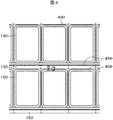
しかし、図3に示すdの部分は捨てられることになるので、マザー基板からの液晶セルの取り出し個数を上げるには不利である。そこで、製造コストの要請から、縦方向においても、隙間を作らず、液晶セルを隣接して形成することが要求されている。
図4は縦方向にも液晶セルを隙間なく配置した例を示すマザー基板の平面図である。図4では、端子部において、隣接する液晶セルと分離線400が共有されている。そうすると、端子部150において、隣接する液晶セルのシール部の構造の影響が現れる。
However, since the portion d shown in FIG. 3 is discarded, it is disadvantageous for increasing the number of liquid crystal cells taken out from the mother substrate. Therefore, due to the demand for manufacturing cost, it is required to form liquid crystal cells adjacent to each other without forming a gap in the vertical direction.
FIG. 4 is a plan view of a mother substrate showing an example in which liquid crystal cells are arranged without gaps in the vertical direction. In FIG. 4, the
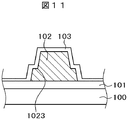
図5は、図4のB−B断面図である。分離線400より左側が端子部150であり、分離線400より右側が図4において下方向に隣接する液晶セルのシール部である。図5において、TFT基板100の上には、絶縁層101が形成されている。絶縁層101は、ゲート絶縁膜、層間絶縁膜等を含む層である。絶縁層101の上に有機パッシベーション膜102が形成されている。有機パッシベーション膜102は、表示領域において、走査線101あるいは映像信号線102等の配線と画素電極あるいはコモン電極とを絶縁する役割を有している。有機パッシベーション膜102は、上記配線と、画素電極あるいはコモン電極との容量カップリングを小さくするために、厚く形成され、例えば、2乃至5μm程度である。
5 is a cross-sectional view taken along the line BB in FIG. The
有機パッシベーション膜102は、図5の領域Aの部分であるスクライビング部においては、スクライビングおよびその後の衝撃による液晶セルの分離を容易にするためのスペーサとしても使用される。したがって、分離線400の部分では、有機パッシベーション膜が土手状に存在している。以降、分離線400に位置する土手状の有機パッシベーション膜を有機パッシベーション膜102Aとして表現する。
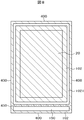
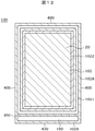
図8は、有機パッシベーション膜が存在している部分を示すTFT基板100の平面図である。図8において、表示領域20には全面に有機パッシベーション膜102が形成されている。また、分離線400、450に対応する部分にも有機パッシベーション膜102Aが形成されている。図8における分離線450は対向基板200側に形成されるので、図8では、対応する場所としての意味で点線450で示している。
The
FIG. 8 is a plan view of the
図8において、表示領域20の外側には、表示領域20を囲むようにして、有機パッシベーション膜102の存在しない、有機パッシベーション膜溝部1021が形成されている。水分は、樹脂を透過して外部から液晶表示パネル内部に侵入するが、有機パッシベーション膜102はアクリル樹脂、シリコン樹脂等の樹脂で形成されているので、この水分を遮断するために有機パッシベーション膜の溝部1021が形成されている。
In FIG. 8, an organic
また、端子部150では、端子の導電部を露出させるため、有機パッシベーション膜は不要である。しかし、分離線400あるいは450においては、スペーサとしての有機パッシベーション膜が必要なので、有機パッシベーション膜102Aが端子部を枠状に囲むように形成されている。
Moreover, in the
図5に戻り、図5の有機パッシベーション膜溝1021は、図8に示す有機パッシベーション膜溝1021に対応するものである。また、分離線400付近を除いては、端子部には有機パッシベーション膜102は形成されていない。図5において、有機パッシベーション膜102、102Aの上には、SiN等によって無機絶縁膜103が形成されている。無機絶縁膜103は、表示領域において、例えば、画素電極とコモン電極を絶縁するために使用される。
Returning to FIG. 5, the organic
図5における端子部150側には、端子が形成されている。端子には表示領域側から延在してきた、例えば、映像信号線と同層で形成された端子金属50が形成されている。端子金属50の上では、無機絶縁膜103にコンタクトホールが形成され、コンタクトホール部分は端子ITO51によって覆われている。ITOは化学的に安定なので、端子金属50を保護する。なお、ITO51は表示領域において画素電極を形成する時に同時に形成することができる。
A terminal is formed on the
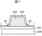
図5における第1の問題点は、ITO51をパターニングする際、ITO残渣52が有機パッシベーション膜102Aの根本に残ってしまうことである。つまり、有機パッシベーション膜102,102Aは、例えば、3μm程度と厚いために、土手状の有機パッシベーション膜102Aの根本が十分に露光されない、または、土手状の有機パッシベーション膜102Aの根本にエッチング液が十分に侵入しないという現象が生ずる。このために、土手状の有機パッシベーション膜102Aの根本にITO残渣52が生ずる。
The first problem in FIG. 5 is that when the
ITO残渣52が発生すると、端子間がITO残渣52によってショートしてしまうという問題を生ずる。図6は、図5の領域Aに対応するTFT基板100側の平面図である。図5の領域Aは、図6におけるC−C断面に対応する。図6において、土手状の有機パッシベーション膜102Aの土手の根本まで、端子を構成するITO51が形成されている。端子と反対側である、シール部側の土手状の有機パッシベーション膜102Aの根本にはITO残渣52が存在している。
When the
ITO残渣52が存在すると、図6に示すように、端子間がショートされてしまうという重大な問題を生ずる。図7は、図6のD−D断面図である。図7において土手状の有機パッシベーション膜102Aの根本には、ITOの残渣52が存在している。図7における土手状の有機パッシベーション膜102Aの左側のITO残渣52が端子間のショートを引き起こす。
If the
このようなITOの残渣52によるショートの問題は、端子部の面積が大きければ、例えば、端子を土手状の有機パッシベーション膜102Aから十分な距離を取って形成する、等の手段をとることも出来るが、表示領域の面積を大きくし、液晶表示パネルの外形を抑えようとすると、端子部の面積を十分にとることができない。
The short-circuit problem caused by the
一方、表示領域において、画素電極が形成された後、液晶を初期配向するために、配向膜104が形成される。配向膜104は、当初は液体であり、フレキソ印刷あるいはインクジェットによって形成される。液体の配向膜材料は、塗布後、流動するので、ストッパーが十分ではないと、マザー基板において、他の液晶セルの端子部にも流入してしまう。
On the other hand, after the pixel electrode is formed in the display region, an
図5はこの問題を示している。図5において、隣接する液晶セルのシール部において、右側の液晶セルの配向膜104はストップされずに、土手状有機パッシベーション膜102Aを超えて左側に隣接する液晶セルの端子の上にまで流入している。配向膜104は、200℃程度で焼成された後、絶縁膜となる。端子に配向膜104が存在すると導通不良を生ずる。したがって、隣接液晶セルからの配向膜104の流入は抑えなければならない。
FIG. 5 illustrates this problem. In FIG. 5, the
図5において、TFT基板100と対向して対向基板200が配置している。対向基板200にはブラックマトリクス201が形成され、その上にカラーフィルタ202が形成されている。カラーフィルタ202は、シール部においては、TFT基板100と対向基板200のギャップの調整に用いられている。このカラーフィルタ202には例えば青カラーフィルタが用いられる。カラーフィルタ201およびブラックマトリクス201を覆ってオーバーコート膜203が形成されている。
In FIG. 5, a
図5において、オーバーコート膜203の上には、壁状スペーサ204が形成されている。壁状スペーサ204は、TFT基板100と対向基板200の間隔を規定する他に、対向基板200側の配向膜104が液晶セルの端部にまで流れ込まないようにする役割も有している。液晶セルと液晶セルの境界の分離線400に対応して土手状スペーサ205が形成されている。壁状スペーサ204も土手状スペーサ205も表示領域において、TFT基板100と対向基板200の間隔を規定する柱状スペーサ等と同じプロセスで形成される。
In FIG. 5, a
図5において、TFT基板100と対向基板200はシール材160によって接着している。シール材160は、シール部のみに存在することが望ましいが、図5においては、土手状スペーサ205と土手状有機パッシベーション膜102Aとの隙間から隣接する液晶セルの端子部にはみ出している。シール材160のはみ出しは、端子の面積が大きければ大きな問題にならないが、高精細になって端子面積が小さくなると導通不良の原因となる。
In FIG. 5, the
このように、液晶セルを隙間なく、マザー基板に配置すると、端子部において、ITO残渣52による端子のショート、配向膜104の隣接液晶セルへの流入による端子の導通不良、シール材160の隣接液晶セルへのはみ出しによる端子の導通不良の問題を生ずる。
As described above, when the liquid crystal cells are arranged on the mother substrate without any gaps, terminal short-circuiting due to the
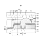
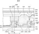
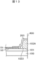
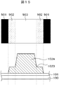
図9はこのような問題を解決する本発明の構成を示す断面図である。図9は、図4におけるB−B断面に相当する。図9において、TFT基板100の上に絶縁層101が形成されている。絶縁層101の上に有機パッシベーション膜102,102Aが形成されている。有機パッシベーション膜102,102Aの役割は図5で説明したものと同様である。図9の特徴は、分離線400に対応する部分における土手状の有機パッシベーション膜102Aが段部1023を有しているということである。土手状の有機パッシベーション膜102Aの底部から段部1023までの高さh1は、例えば1μmであり、段部1023から土手状の有機パッシベーション膜102Aの頂点までの高さh2は、例えば2μmである。
FIG. 9 is a cross-sectional view showing a configuration of the present invention for solving such a problem. FIG. 9 corresponds to the BB cross section in FIG. In FIG. 9, an insulating
ITOの残渣52は、土手状の有機パッシベーション膜102Aの溝の深さが2μmを超えると急激に増加する。図9では、土手状有機パッシベーション膜102Aは段部1023を有しているので、有機パッシベーション膜溝1021の深さは2μmと1μmとで段階的に分かれており、いずれの深さもITO残渣52が発生しにくい深さとなっている。しがって、図5の場合と異なり、端子ITO51のショートを防止することができる。
The
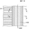
図10は、図9の領域Bに対応するTFT基板100の平面図である。図9のTFT基板100側における領域Bは、図10のE−E断面に相当する。図9および図10に示すように、土手状有機パッシベーション膜102Aの段部1023にも根本にもITOの残渣は存在していない。
図11は、図10のF−F断面図である。図10および図11に示すように、土手状有機パッシベーション膜102Aのいずれの段部1023にも、また、土手状有機パッシベーション膜102Aの根本にもITOの残渣は存在しない。したがって、ITOの残渣によって端子ITO51がショートされるということは無い。
FIG. 10 is a plan view of the
11 is a cross-sectional view taken along line FF in FIG. As shown in FIGS. 10 and 11, there is no ITO residue at any
図9の他の特徴は、土手状スペーサ205の先端に凹部が形成され、この凹部に土手状有機パッシベーション膜102Aの先端が挿入されていることである。言い換えると、土手状有機パッシベーション膜102Aの先端が土手状スペーサ205の凹部に対向している。このように、土手状有機パッシベーション膜102Aの先端が土手状スペーサ205に形成された凹部に挿入されていることによって、シール材160が隣接する液晶セルの端子部にはみ出しにくい構成となっている。したがって、はみ出したシール材160によって隣接する液晶セルの端子を覆って導通不良を生じさせる現象を回避することができる。なお、図9における凹部は、土手状有機パッシベーション膜102Aが挿入されるものであるから、溝状に形成されている。
Another feature of FIG. 9 is that a recess is formed at the tip of the bank-
図9のさらに他の特徴は、有機パッシベーション膜溝1021のさらに内側に第2の有機パッシベーション膜の溝1022が形成され、その結果第2の土手状有機パッシベーション膜102が形成されていることである。第2の有機パッシベーション膜溝1022の深さは、第1の有機パッシベーション膜溝1021の深さよりも浅く、h2である。h2は例えば2μmである。したがって、第2の有機パッシベーション膜溝1022の底は、絶縁層101でなく、有機パッシベーション膜102となっている。
Still another feature of FIG. 9 is that a
図9に示すように、第2の有機パッシベーション膜溝1022が存在することによる第2の土手状有機パッシベーション膜102によって、配向膜の流れを阻止することができる。また、第2の土手状有機パッシベーション膜102によって配向膜をストップできない場合であっても、第1の土手状有機パッシベーション膜102によって配向膜104の流れを阻止することができる。
As shown in FIG. 9, the flow of the alignment film can be prevented by the second bank-like
図12は、TFT基板100における、有機パッシベーション膜102の形状を示す平面図である。有機パッシベーション膜102の平面図の基本的な構成は図8で説明したものと同様である。図12が図8と異なる点は、有機パッシベーション膜溝1021の内側、すなわち、表示領域20側に第2の有機パッシベーション膜溝1022が形成されていることである。
FIG. 12 is a plan view showing the shape of the
第2の有機パッシベーション膜溝1022の深さは、図9に示すh2であり、例えば2μmである。第1の有機パッシベーション膜溝1021の深さはh1+h2であり、例えば3μmである。したがって、第1の有機パッシベーション膜溝1021の方が、配向膜104をストップする能力は優れているが、本発明では、第2の有機パッシベーション膜溝1022を加えることによって、配向膜104の流れをストップする機会をより多くしている。
The depth of the second organic
なお、図9において、溝の深さの関係は、h2>h1である。あるいは、h1<(h1+h2)/2である。このような構成とすることによって、第2の有機パッシベーション膜溝1022による配向膜104の流れを阻止する効果をより上げることができる。
In FIG. 9, the relationship between the depths of the grooves is h2> h1. Alternatively, h1 <(h1 + h2) / 2. By adopting such a configuration, the effect of preventing the flow of the
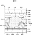
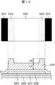
図13および図14は、マザー基板に形成された隣接する液晶セルを分離線400において分離した場合の、第1の液晶セルの端子部の断面図と第1のセルに隣接する第2の液晶セルにおけるシール部の断面図である。図13は、第1の液晶セルの端子部の断面図である。図13においては、対向基板側は、図2における端材210として捨てられるので、TFT基板100側の構成のみが残っている。
13 and 14 are a cross-sectional view of the terminal portion of the first liquid crystal cell and the second liquid crystal adjacent to the first cell when the adjacent liquid crystal cell formed on the mother substrate is separated by the
図13において、TFT基板100の上に絶縁層101が形成され、その上に段部1023を有する土手状有機パッシベーション膜102Aの片側が残っている。図13において、土手状有機パッシベーション膜102の根本には、ITOの残渣は存在していないので、端子がITOの残渣によってショートされる危険はない。また、シール材の端子へのはみ出しも配向膜の端子への流入もないので、端子の接続不良は回避することができる。
In FIG. 13, the insulating
図14は第1の液晶セルに隣接する第2の液晶セルのシール部の断面図である。図14において、土手状スペーサ205と土手状有機パッシベーション膜102Aは、分離線400によって半分に分断されている。図14のこの構成を言い換えると、土手状スペーサ205は第1の部分と、縁部であって、第1の部分よりも膜厚の大きい第2の部分を有し、土手状有機パッシベーション膜102Aの先端は、土手状スペーサ205の第1の部分と対向していると言い換えることが出来る。
FIG. 14 is a cross-sectional view of the seal portion of the second liquid crystal cell adjacent to the first liquid crystal cell. In FIG. 14, the bank-
その他の構成は、図9において説明したとおりである。このように、本発明によれば、マザー基板内に液晶セルを隙間なく連続して配置しても、隣接する液晶セルのシール部の影響による、端子の接続不良、あるいは、ITO残渣による端子のショートを防止することができる。 Other configurations are as described in FIG. As described above, according to the present invention, even if the liquid crystal cells are continuously arranged in the mother substrate without gaps, the terminal connection failure due to the influence of the seal portion of the adjacent liquid crystal cell or the terminal due to the ITO residue Short circuit can be prevented.
図15は、図9における土手状有機パッシベーション膜102Aに段部1023を設ける方法を示す模式断面図である。有機パッシベーション膜102Aは感光性の樹脂が使用される。この感光性の樹脂は、光が照射された部分において、樹脂が硬化し、光が当たらない部分は、現像液によって除去される。
FIG. 15 is a schematic cross-sectional view showing a method for providing a stepped
図15において、土手状有機パッシベーション膜102Aの段部1023は、ハーフ露光によって形成することができる。段部1023の高さは、ハーフ露光における光の強度によって調整することができる。すなわち、土手状有機パッシベーション膜102Aとして有機パッシベーション膜をフルに残したい部分は、マスクの透過領域503を通してフル露光を行い、有機パッシベーション膜を除去したい部分にはマスクの遮光領域501を対応させる。そして、有機パッシベーション膜の段部1023に続く膜厚の小さい部分は、マスクのハーフトーン部502を通して露光することにより形成することができる。
In FIG. 15, the
図16は、対向基板200において、凹部を有する土手状スペーサ205を形成する方法を示す模式断面図である。土手状スペーサ205の凹部もハーフ露光技術を用いて形成することができる。土手状スペーサ205には例えば感光性のアクリル樹脂を用いることができる。図16において、土手状スペーサ205の両側の膜厚が大きい部分はマスクの透明部分503を介してフル露光を行う。土手状スペーサ205を除去したい部分には、マスクの遮光部分501を対応させる。土手状スペーサ205の凹部の部分にはマスクのハーフトーン部502を対応させて露光し、所定の厚さとする。図16において、土手状スペーサ205の凹部の深さh4あるいは土手状スペーサの凹部における土手状スペーサの厚さh3は、ハーフ露光の露光強度を調整することによって制御することができる。
FIG. 16 is a schematic cross-sectional view showing a method of forming a bank-
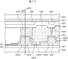
図17は、本発明の他の構成を示す断面図である。土手状スペーサ205の凹部に土手状有機パッシベーション膜102Aを挿入する目的は、シール材160を端子部側にはみ出させないことである。この目的のためには、土手状スペーサ205の縁部2051は、土手状有機パッシベーション膜102Aの両側ではなく、片側に存在していればよい。図16は、端子側の縁部を省略してシール部側にのみ土手状スペーサの縁部2051を形成したものである。
FIG. 17 is a cross-sectional view showing another configuration of the present invention. The purpose of inserting the bank-like
この構成であれば、土手状有機パッシベーション膜102Aを土手状スペーサ205の凹部に挿入する必要がないので、TFT基板100と対向基板200の位置合わせが容易になるというメリットを有する。図17のその他の構成は図9と同様である。
With this configuration, since it is not necessary to insert the bank-like
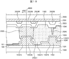
図18は、本発明のさらに他の変形例を示す断面図である。図18が図9と異なる点は、土手状スペーサ205の高さを調整するカラーフィルタを2層用いている点である。つまり、土手状スペーサ205の縁部2051に対応して赤カラーフィルタ202Rを配置し、この部分は、赤カラーフィルタ202Rと青カラーフィルタ202Bの積層となっている。一方、土手状スペーサの他の部分には、青カラーフィルタ202Bのみ形成されている。
FIG. 18 is a cross-sectional view showing still another modification of the present invention. 18 differs from FIG. 9 in that two layers of color filters for adjusting the height of the bank-
すなわち、土手状スペーサ205の縁部2051では、土台が高くなっているので、縁部の高さと凹部の高さの差をつけやすい。言い換えると、土手状スペーサ205の凹部を形成するために、ハーフ露光にたよる割合を小さくすることができ、その分ハーフ露光のプロセス条件の裕度を上げることができる。図18のその他の構成は図9と同様である。
That is, since the base is high at the
図17の構成も図18の構成も、図9の構成の場合と同様の効果を得ることができる。 The configuration of FIG. 17 and the configuration of FIG. 18 can achieve the same effects as the configuration of FIG.
11…走査線、 12…映像信号線、 13…画素、 20…表示領域、 50…端子金属、 51…端子ITO、 52…ITO残渣、 100…TFT基板、 101…絶縁層、 102、102A…有機パッシベーション膜、 103…無機絶縁膜、 104…配向膜、 150…端子部、 160…シール材、 200…対向基板、 201…ブラックマトリクス、 202…カラーフィルタ、 202B…青カラーフィルタ、 202R…赤カラーフィルタ、 203…オーバーコート膜、 204…壁状スペーサ、 205…土手状スペーサ、 210…端材、 300…液晶、 400、450…分離線、 501…マスクの遮光部、 502…マスクのハーフトーン部、 503…マスクの透過部、 1021…有機パッシベーション膜溝、 1022…有機パッシベーション膜の第2の溝、 1023…有機パッシベーション膜の段部
DESCRIPTION OF
Claims (13)
前記TFT基板には、前記端子部が形成されている前記TFT基板縁部に沿って土手状の有機パッシベーション膜が形成され、
前記有機パッシベーション膜の前記端子部側の側面には、少なくとも一つの段差部が形成されることを特徴とする液晶表示装置。 A liquid crystal display device in which a TFT substrate and a counter substrate are bonded to each other at a seal portion formed around the counter substrate, and a terminal portion is formed in a portion of the TFT substrate that is not opposed to the counter substrate;
On the TFT substrate, a bank-like organic passivation film is formed along the TFT substrate edge on which the terminal portion is formed,
The liquid crystal display device according to claim 1, wherein at least one step portion is formed on a side surface of the organic passivation film on the terminal portion side.
前記端子部が形成された辺と反対側の辺において、
前記TFT基板には、当該対向基板縁部に沿って土手状の第1の有機パッシベーション膜が形成され、
前記第1の有機パッシベーション膜の表示領域側の側面には、少なくとも一つの段差部が形成され、
前記対向基板には、前記第1の有機パッシベーション膜に対応する位置に第1のスペーサが形成され、
前記第1の有機パッシベーション膜の先端は、前記第1のスペーサと対向していることを特徴とする液晶表示装置。 A TFT substrate having an organic passivation film, a counter substrate, the TFT substrate and the counter substrate are bonded to each other at a seal portion formed around the counter substrate, and the portion of the TFT substrate where the counter substrate does not face A liquid crystal display device in which a terminal portion is formed and a display region is formed in a region surrounded by the seal portion,
On the side opposite to the side where the terminal portion is formed,
On the TFT substrate, a bank-like first organic passivation film is formed along the counter substrate edge,
At least one step portion is formed on the side surface of the first organic passivation film on the display region side,
A first spacer is formed on the counter substrate at a position corresponding to the first organic passivation film,
A liquid crystal display device, wherein a tip of the first organic passivation film is opposed to the first spacer.
前記第1及び第2の有機パッシベーション膜の間に第1の溝が形成され、前記第2の有機パッシベーション膜の表示領域側には第2の溝が形成され、
前記第2の有機パッシベーション膜の側面には、少なくとも一つの段差部が形成されることを特徴とする請求項4に記載の液晶表示装置。 A bank-like second organic passivation film is formed on the display area side of the first organic passivation film so as to surround the display area,
A first groove is formed between the first and second organic passivation films, and a second groove is formed on the display region side of the second organic passivation film;
The liquid crystal display device according to claim 4, wherein at least one step portion is formed on a side surface of the second organic passivation film.
前記TFT基板には、前記液晶セルの縁領域に沿って土手状の第1の有機パッシベーション膜が形成され、前記各液晶セルの表示領域内には第2の有機絶縁膜が形成され、
前記第1の有機パッシベーション膜と前記第2の有機パッシベーション膜の間には、前記第2の有機パッシベーション膜を取り囲む形で第1の溝部が形成され、
前記第1の有機パッシベーション膜は、前記液晶セルごとに、端子部用の開口領域として第2の溝部が形成され、
前記第1の溝部と前記第2の溝部にある前記第1の有機パッシベーション膜で各液晶セルの分断領域となることを特徴とするマザー基板。 In a mother substrate in which a plurality of liquid crystal cells are formed by bonding a TFT substrate and a counter substrate by a plurality of seal portions formed for each display region,
On the TFT substrate, a bank-like first organic passivation film is formed along an edge region of the liquid crystal cell, and a second organic insulating film is formed in the display region of each liquid crystal cell,
A first groove is formed between the first organic passivation film and the second organic passivation film so as to surround the second organic passivation film,
In the first organic passivation film, a second groove portion is formed as an opening region for a terminal portion for each liquid crystal cell,
A mother substrate, wherein the first organic passivation film in the first groove and the second groove serves as a dividing region of each liquid crystal cell.
Priority Applications (2)
| Application Number | Priority Date | Filing Date | Title |
|---|---|---|---|
| JP2016055280A JP2017167478A (en) | 2016-03-18 | 2016-03-18 | Liquid crystal display device and mother substrate for the same |
| US15/450,405 US10209576B2 (en) | 2016-03-18 | 2017-03-06 | Liquid crystal display device and mother substrate thereof |
Applications Claiming Priority (1)
| Application Number | Priority Date | Filing Date | Title |
|---|---|---|---|
| JP2016055280A JP2017167478A (en) | 2016-03-18 | 2016-03-18 | Liquid crystal display device and mother substrate for the same |
Publications (1)
| Publication Number | Publication Date |
|---|---|
| JP2017167478A true JP2017167478A (en) | 2017-09-21 |
Family
ID=59855523
Family Applications (1)
| Application Number | Title | Priority Date | Filing Date |
|---|---|---|---|
| JP2016055280A Pending JP2017167478A (en) | 2016-03-18 | 2016-03-18 | Liquid crystal display device and mother substrate for the same |
Country Status (2)
| Country | Link |
|---|---|
| US (1) | US10209576B2 (en) |
| JP (1) | JP2017167478A (en) |
Cited By (5)
| Publication number | Priority date | Publication date | Assignee | Title |
|---|---|---|---|---|
| KR20190079738A (en) * | 2017-12-27 | 2019-07-08 | 삼성디스플레이 주식회사 | Method for manufacturing display device |
| JP2019159232A (en) * | 2018-03-16 | 2019-09-19 | 凸版印刷株式会社 | Liquid crystal display device |
| WO2020179244A1 (en) * | 2019-03-01 | 2020-09-10 | 株式会社ジャパンディスプレイ | Display device |
| JP2022092232A (en) * | 2020-12-10 | 2022-06-22 | 株式会社ジャパンディスプレイ | Liquid crystal device |
| JP2023507054A (en) * | 2019-12-19 | 2023-02-21 | グーグル エルエルシー | Power line design for sensors in display panels |
Families Citing this family (2)
| Publication number | Priority date | Publication date | Assignee | Title |
|---|---|---|---|---|
| US10866465B2 (en) * | 2019-03-25 | 2020-12-15 | Himax Display, Inc. | Display panel and manufacturing method thereof |
| CN112133734B (en) * | 2020-09-29 | 2022-08-30 | 湖北长江新型显示产业创新中心有限公司 | Display panel and display device |
Family Cites Families (4)
| Publication number | Priority date | Publication date | Assignee | Title |
|---|---|---|---|---|
| JP3172167B2 (en) * | 1990-07-12 | 2001-06-04 | セイコーエプソン株式会社 | Electro-optical device and method of manufacturing electro-optical device |
| JP4783115B2 (en) * | 2005-10-18 | 2011-09-28 | 東芝モバイルディスプレイ株式会社 | Board device |
| JP5395259B2 (en) | 2010-04-23 | 2014-01-22 | シャープ株式会社 | Method for forming dividing guide groove, liquid crystal mother panel, and dividing method |
| JP2013029722A (en) * | 2011-07-29 | 2013-02-07 | Sony Corp | Display and electronic unit |
-
2016
- 2016-03-18 JP JP2016055280A patent/JP2017167478A/en active Pending
-
2017
- 2017-03-06 US US15/450,405 patent/US10209576B2/en active Active
Cited By (8)
| Publication number | Priority date | Publication date | Assignee | Title |
|---|---|---|---|---|
| KR20190079738A (en) * | 2017-12-27 | 2019-07-08 | 삼성디스플레이 주식회사 | Method for manufacturing display device |
| KR102341854B1 (en) | 2017-12-27 | 2021-12-23 | 삼성디스플레이 주식회사 | Method for manufacturing display device |
| JP2019159232A (en) * | 2018-03-16 | 2019-09-19 | 凸版印刷株式会社 | Liquid crystal display device |
| WO2020179244A1 (en) * | 2019-03-01 | 2020-09-10 | 株式会社ジャパンディスプレイ | Display device |
| JP2023507054A (en) * | 2019-12-19 | 2023-02-21 | グーグル エルエルシー | Power line design for sensors in display panels |
| JP7564871B2 (en) | 2019-12-19 | 2024-10-09 | グーグル エルエルシー | Power Line Design for Sensors in Display Panels |
| JP2022092232A (en) * | 2020-12-10 | 2022-06-22 | 株式会社ジャパンディスプレイ | Liquid crystal device |
| JP7558783B2 (en) | 2020-12-10 | 2024-10-01 | 株式会社ジャパンディスプレイ | Liquid Crystal Devices |
Also Published As
| Publication number | Publication date |
|---|---|
| US10209576B2 (en) | 2019-02-19 |
| US20170269404A1 (en) | 2017-09-21 |
Similar Documents
| Publication | Publication Date | Title |
|---|---|---|
| US11852923B2 (en) | Liquid crystal display device | |
| JP5553531B2 (en) | Liquid crystal display | |
| US10473984B2 (en) | Liquid crystal display device | |
| JP2017167478A (en) | Liquid crystal display device and mother substrate for the same | |
| US9575370B2 (en) | Liquid crystal display device | |
| JP6649788B2 (en) | Liquid crystal display | |
| JP5156517B2 (en) | Liquid crystal display | |
| JP2017111290A (en) | Liquid crystal display device | |
| JP2016109807A (en) | Liquid crystal display device | |
| JP2004272012A (en) | Display apparatus | |
| JP5563020B2 (en) | Liquid crystal display | |
| JP5275650B2 (en) | Liquid crystal display | |
| WO2016157399A1 (en) | Liquid crystal panel and liquid crystal display device | |
| JP2020074029A (en) | Liquid crystal display | |
| JP7183366B2 (en) | liquid crystal display | |
| JP6367415B2 (en) | Liquid crystal display | |
| JP2009251565A (en) | Method for manufacturing liquid crystal display device | |
| JP5492326B2 (en) | Manufacturing method of liquid crystal display device | |
| JP6121508B2 (en) | Liquid crystal display device and manufacturing method thereof | |
| JP2019082738A (en) | Liquid crystal display | |
| JP2005037763A (en) | Liquid crystal display device | |
| WO2016151860A1 (en) | Method for forming contact hole of liquid crystal panel, liquid crystal panel, and liquid crystal display | |
| JP2010175607A (en) | Liquid crystal display device | |
| KR20070023971A (en) | LCD and its manufacturing method |