JP2017162429A - Information processing device and method, and program - Google Patents
Information processing device and method, and program Download PDFInfo
- Publication number
- JP2017162429A JP2017162429A JP2016107545A JP2016107545A JP2017162429A JP 2017162429 A JP2017162429 A JP 2017162429A JP 2016107545 A JP2016107545 A JP 2016107545A JP 2016107545 A JP2016107545 A JP 2016107545A JP 2017162429 A JP2017162429 A JP 2017162429A
- Authority
- JP
- Japan
- Prior art keywords
- rule
- layout
- layout verification
- comparison
- information
- Prior art date
- Legal status (The legal status is an assumption and is not a legal conclusion. Google has not performed a legal analysis and makes no representation as to the accuracy of the status listed.)
- Pending
Links
Images


Abstract
Description
本発明は、例えばLSI又はICなどの半導体集積回路のレイアウト検証用ルールを修正するための情報処理装置及び方法、並びにプログラムに関する。 The present invention relates to an information processing apparatus and method for correcting a layout verification rule of a semiconductor integrated circuit such as an LSI or an IC, and a program.
半導体集積回路の設計では、マスクパターンと呼ばれるレイアウトが製造プロセスで規定されるデザインルールを満たしているかどうかをチェックするレイアウト検証工程が行われる。レイアウト検証工程は、レイアウト検証用ツール(DRC(Design Rule Check)ツール)にデザインルール及び該ツールのコマンドが記述されたレイアウト検証用デザインルールのファイルを入力することにより行われる。以下、レイアウト検証用デザインルールを「DRCルール」という。また、DRCルールのファイルを「DRCルールファイル」という。 In designing a semiconductor integrated circuit, a layout verification process is performed to check whether a layout called a mask pattern satisfies a design rule defined by a manufacturing process. The layout verification process is performed by inputting a layout verification design rule file in which design rules and commands of the tool are described in a layout verification tool (DRC (Design Rule Check) tool). Hereinafter, the design rule for layout verification is referred to as “DRC rule”. The DRC rule file is referred to as a “DRC rule file”.
すなわち、このDRCルールファイルに誤りが含まれていると正確なレイアウト検証が出来ないため、デザインルールを満たしていないレイアウトが作成されることになり、半導体回路の設計品質の低下を招く。DRCルールファイルは手動で作成されるか、または、ツールなどにより自動で作成された後に手動で修正されることがあるため、誤りを含んでいることが多い。そのため、DRCルールファイル自体が正しく作成されているかを検証用のテストパターンを用いてチェックする必要があることが既に知られている(例えば、特許文献1参照)。 That is, if the DRC rule file contains an error, accurate layout verification cannot be performed, and a layout that does not satisfy the design rule is created, resulting in a reduction in the design quality of the semiconductor circuit. Since the DRC rule file is manually created or may be manually modified after being automatically created by a tool or the like, it often contains errors. For this reason, it is already known that it is necessary to check whether the DRC rule file itself is correctly created using a test pattern for verification (see, for example, Patent Document 1).
また、上記レイアウト検証工程において、レイアウト検証用ツール(LVS(Layout Versus Schematic)ツール)に、該ツールのコマンドが記述されたLVSルールを入力することにより行われる(例えば、非特許文献2参照)。すなわち、このLVSルールに誤りが含まれていると正確なレイアウト検証が出来ないため、回路情報を満たしていないレイアウトが作成されることになり、半導体回路の設計品質の低下を招く。LVSルールを正確に作成するためには、検証用のデバイスレイアウトパターンを用いてそのルール内容をチェックしながら作成することが既に知られている。以下、レイアウト検証用デバイスレイアウトルールを「LVSルール」という。また、LVSルールのファイルを「LVSルールファイル」という。 In the layout verification step, the LVS rule in which the command of the tool is described is input to a layout verification tool (LVS (Layout Versus Schematic) tool) (see, for example, Non-Patent Document 2). That is, if an error is included in the LVS rule, accurate layout verification cannot be performed, so that a layout that does not satisfy the circuit information is created, and the design quality of the semiconductor circuit is degraded. In order to accurately create an LVS rule, it is already known to create a LVS rule while checking the content of the rule using a device layout pattern for verification. Hereinafter, the device layout rule for layout verification is referred to as “LVS rule”. An LVS rule file is referred to as an “LVS rule file”.
しかし、今までのテストパターンを用いたDRCルールファイルの検証では、レイアウト検証を実施し、得られる検証結果がデザインルールと照合して妥当なものかを判断し、その結果から手動でDRCルールファイルを修正する方法を取っているため、多大な労力を必要とするという問題があった。また、LVSルールファイルの修正についても同様の問題があった。 However, in the verification of the DRC rule file using the conventional test pattern, the layout verification is performed, and it is determined whether the obtained verification result is appropriate by comparing with the design rule, and the DRC rule file is manually determined from the result. There is a problem that a great deal of labor is required. Also, there was a similar problem with the modification of the LVS rule file.
本発明の目的は以上の問題点を解決し、レイアウト検証用ルールの検証工程において、従来技術に比較して修正処理の工数を削減でき、当該ルールの修正効率を高めることができる情報処理装置を提供することにある。 An object of the present invention is to provide an information processing apparatus that solves the above-described problems and can reduce the number of man-hours for correction processing in the layout verification rule verification process as compared with the prior art and can improve the correction efficiency of the rules. It is to provide.
本発明にかかる情報処理装置は、半導体集積回路のレイアウトを検証する際に使用されるレイアウト検証用ルールを検証する情報処理装置において、
上記レイアウト検証用ルールを検証する際に使用されるレイアウト検証用パターンを、上記レイアウト検証用ルールと比較し、比較結果である差分を含む比較情報を生成する比較手段を備えたことを特徴とする。
An information processing apparatus according to the present invention is an information processing apparatus that verifies a layout verification rule used when verifying a layout of a semiconductor integrated circuit.
Comparing means for comparing a layout verification pattern used when verifying the layout verification rule with the layout verification rule, and generating comparison information including a difference as a comparison result. .
本発明にかかる情報処理装置によれば、レイアウト検証用ルールの検証工程において、従来技術に比較して修正処理の工数を削減でき、当該ルールの修正効率を高めることができる。 According to the information processing apparatus of the present invention, in the verification process of the layout verification rule, the number of correction processes can be reduced as compared with the prior art, and the correction efficiency of the rule can be increased.
以下、本発明に係る実施形態について図面を参照して説明する。なお、以下の各実施形態において、同様の構成要素については同一の符号を付している。 Hereinafter, embodiments according to the present invention will be described with reference to the drawings. In addition, in each following embodiment, the same code | symbol is attached | subjected about the same component.
図1は本発明の一実施形態にかかるレイアウト検証用ルールファイル修正装置である情報処理装置1を含む情報処理システムの構成を示すブロック図である。本実施形態にかかる情報処理装置1は、半導体集積回路のレイアウトを検証する際に使用されるレイアウト検証用デザインルール(DRCルール)及びレイアウト検証用デバイスレイアウトルール(LVSルール)を検証するために提供される。情報処理装置1は、レイアウト検証用デザインルールを、そのデザインルールに対応するレイアウト検証用テストパターンと比較し、その比較結果に基づいてDRCルールファイルを修正するDRCルール比較修正処理部10を備える。情報処理装置1は、レイアウト検証用デバイスレイアウトルールをそのデバイスレイアウトルールに対応するレイアウト検証用デバイスレイアウトパターンと比較しその比較結果に基づいてLVSルールファイルを修正するLVSルール比較修正処理部50を備える。ここで、レイアウト検証用デザインルール(DRCルール)及びレイアウト検証用デバイスレイアウトルール(LVSルール)を総称して、「レイアウト検証用ルール」という。また、レイアウト検証用テストパターン及びレイアウト検証用デバイスレイアウトパターンを総称して、「レイアウト検証用パターン」という。
FIG. 1 is a block diagram showing a configuration of an information processing system including an
図1の情報処理システムは、DRCルール比較修正処理部10及びLVSルール比較修正処理部50を備えた情報処理装置1と、所定のデータファイル及びコマンドを入力するキーボード2と、コマンド等を入力するマウス3と、記憶装置4と、表示装置5とを備える。ここで、情報処理装置1は、例えばデジタル計算機などのコンピュータである。
The information processing system in FIG. 1 inputs an
情報処理装置1のDRCルール比較修正処理部10は、キーボード2及びマウス3からの入力や記憶装置4に記憶されたデータなどに基づいて、図3のDRCルール比較修正処理(図4のDRCルール修正サブルーチン処理を含む)を実行する。そして、DRCルール比較修正処理部10は、処理結果である修正後のDRCルールを表示装置5に表示し、記憶装置4に書き込む。また、情報処理装置1のLVSルール比較修正処理部50は、キーボード2及びマウス3からの入力や記憶装置4に記憶されたデータなどに基づいて、図10のLVSルール比較修正処理(図11のLVSルール修正サブルーチン処理を含む)を実行する。そして、LVSルール比較修正処理部50は、処理結果である修正後のLVSルールを表示装置5に表示し、記憶装置4に書き込む。
The DRC rule comparison /
キーボード2は、DRCルール比較修正処理のためのコマンド等を入力する。マウス3は、DRCルール比較修正処理のためのコマンド入力の補助手段として、入力や表示に際してGUI(Graphical User Interface)で指示を行う場合に使用する。ここで、マウス3に限らずタブレット、トラックボール等のポインティングデバイスを用いてもよい。
The
記憶装置4は、テストパターンファイル11と、DRCルールファイル12と、修正後DRCルールファイル13と、比較情報ファイル14とを備えて構成される。また、記憶装置4は、デバイスレイアウトパターンファイル51と、LVSルールファイル52と、修正後LVSルールファイル53と、比較情報ファイル54とを備えて構成される。表示装置5は、キーボード2やマウス3からの入力に応じて、実行状態や結果ファイルの表示を行う。
The
図2は図1の情報処理装置1により実行されるルール比較修正処理の判断実行処理を示すフローチャートである。
FIG. 2 is a flowchart showing the determination execution process of the rule comparison correction process executed by the
図2のステップS1において、DRCルール比較修正処理と、LVSルール比較修正処理との両方を実行するか否かが判断され、YESのときはステップS2に進む一方、NOのときはステップS4に進む。ステップS2において、DRCルール比較修正処理を実行し、ステップS3においてLVSルール比較修正処理を実行して当該判断実行処理を終了する。ステップS4において、DRCルール比較修正処理のみを実行するか否かが判断され、YESのときはステップS5に進む一方、NOのときはステップS6に進む。ステップS5においてDRCルール比較修正処理を実行して当該判断実行処理を終了する。ステップS6においてLVSルール比較修正処理のみを実行するか否かが判断され、YESのときはステップS7に進む一方、NOのときは当該判断実行処理を終了する。ステップS7においてLVSルール比較修正処理を実行して当該判断実行処理を終了する。 In step S1 of FIG. 2, it is determined whether or not both the DRC rule comparison / correction process and the LVS rule comparison / correction process are executed. If YES, the process proceeds to step S2, while if NO, the process proceeds to step S4. . In step S2, a DRC rule comparison / correction process is executed. In step S3, an LVS rule comparison / correction process is executed, and the determination execution process ends. In step S4, it is determined whether or not only the DRC rule comparison / correction process is executed. If YES, the process proceeds to step S5. If NO, the process proceeds to step S6. In step S5, the DRC rule comparison / correction process is executed, and the determination execution process ends. In step S6, it is determined whether or not only the LVS rule comparison / correction process is executed. If YES, the process proceeds to step S7. If NO, the determination execution process is terminated. In step S7, the LVS rule comparison / correction process is executed, and the determination execution process ends.
次いで、図1のDRCルール比較修正処理部10の動作を図3のフローチャートを参照して説明する。
Next, the operation of the DRC rule comparison /
図3は図1の情報処理装置1のDRCルール比較修正処理部10により実行されるDRCルール比較修正処理(S2,S5)を示すフローチャートである。図3のDRCルール比較修正処理及び図4のDRCルール修正サブルーチン処理は、図1の情報処理装置1のDRCルール比較修正処理部10により実行されるプログラムの形式で提供される。なお、テストパターン及びDRCルールは予め記憶装置4内のテストパターンファイル11及びDRCルールファイル12にそれぞれ格納される。ここで、テストパターンファイル11内のテストパターンは、デザインルールが指定する値と一致するように、ちょうどにレイアウトされたパターンが格納されている。これらの情報をDRCルール比較修正処理部10に入力することで、DRCルールファイル12に間違いがあった場合、その箇所が修正された修正後DRCルールファイル13が生成されて出力される。
FIG. 3 is a flowchart showing DRC rule comparison / correction processing (S2, S5) executed by the DRC rule comparison /
図3のステップS11において、記憶装置4内のテストパターンファイル11からテストパターンを読み出し、ステップS12において記憶装置4内のDRCルールファイル12からDRCルールを読み出す。次いで、ステップS13において、テストパターンに基づいてDRCルールを修正して、修正後のDRCルールを生成する。さらに、ステップS14において、生成された記憶装置4内の修正後のDRCルールを、修正後DRCルールファイル13に書き込むとともに、表示装置5に表示し、当該DRCルール比較修正処理を終了し、元のメインルーチンに戻る。
In step S11 of FIG. 3, a test pattern is read from the
図4は図3のサブルーチンであるDRCルール修正サブルーチン処理(S13)を示すフローチャートである。 FIG. 4 is a flowchart showing a DRC rule correction subroutine process (S13) which is the subroutine of FIG.
図4のステップS21において、テストパターンで設定されている値を、DRCルールで規定されている値と比較する。テストパターンで設定されている値は例えば、テストパターンのパターン名、メタル配線の最小幅や最小間隔などである。DRCルールで規定されている値は、テストパターンのパターン名に対応するメタル配線の最小幅や最小間隔などである。ステップS22において、比較結果に基づき、当該比較結果の差分(テストパターンとDRCルールとの相違点又は不一致を含む差分)があるか否かが判断される。ステップS22において、比較結果に基づき、当該比較結果の差分(テストパターンとDRCルールとの相違点又は不一致を含む差分)があるか否かが判断される。ステップS22において、YESのときはステップS23に進む一方、NOのときは元のメインルーチンに戻る。ステップS23において、比較結果に基づき比較情報を含む比較情報ファイルを生成して記憶装置4内の比較情報ファイル14に書き込む。次いで、ステップS24において、比較情報ファイル14の比較情報に基づいてDRCルールを修正した後、元のメインルーチンに戻る。
In step S21 in FIG. 4, the value set in the test pattern is compared with the value specified in the DRC rule. The values set in the test pattern are, for example, the pattern name of the test pattern, the minimum width and the minimum interval of the metal wiring. The values defined by the DRC rule are the minimum width and minimum interval of the metal wiring corresponding to the pattern name of the test pattern. In step S22, based on the comparison result, it is determined whether or not there is a difference (a difference including a difference or mismatch between the test pattern and the DRC rule). In step S22, based on the comparison result, it is determined whether or not there is a difference (a difference including a difference or mismatch between the test pattern and the DRC rule). If YES in step S22, the process proceeds to step S23. If NO, the process returns to the original main routine. In
図5A〜図5Cはそれぞれ図3のDRCルール比較修正処理において用いるテストパターンの構成例1〜3を示す平面図である。 5A to 5C are plan views showing configuration examples 1 to 3 of test patterns used in the DRC rule comparison and correction process of FIG.
図5Aは、2つの四角形21,22を含むパターンの外側エッジの間隔d1が所定値以上を満足しなければならないデザインルールに対するテストパターンである。ここで、2つの四角形21,22は、レイアウト上のレイヤー、例えば、ポリシリコンのレイヤーであり、隣接するポリシリコンの間隔をチェックするパターンとなっている。
FIG. 5A shows a test pattern for a design rule in which the distance d1 between the outer edges of a pattern including two
図5Bは、外側の四角形23と、その中にある内側の四角形24とを含むパターンであって、異なる層のエッジ間隔d2が所定値以上を満足しなければならないデザインルールに対するテストパターンである。ここで、内側の四角形24は、例えば、第1のビアのレイヤーであり、外側の四角形23は、例えば第1のメタルのレイヤーであり、第1のビアを第1のメタルが包含する余裕度をチェックするパターンとなっている。
FIG. 5B shows a test pattern for a design rule that includes an
図5Cは、1つの四角形25を含むパターンであって、当該パターンの内側エッジの間隔d3が所定値以上を満足しなければならないデザインルールに対するテストパターンとなっている。ここで、四角形25はレイアウト上のレイヤー、例えば、第1のメタルのレイヤーであり、その第1のメタルの幅をチェックするパターンとなっている。
FIG. 5C shows a pattern including one
図5A〜図5Cのそれぞれの各テストパターンは、デザインルールの値と同一の値でレイアウトされている。例えば、パターンの外側エッジの間隔がデザインルールで0.1μm以上との規定である場合、図5Aの間隔d1は、上記と同一である0.1μmでレイアウトされている。 Each test pattern in FIGS. 5A to 5C is laid out with the same value as the value of the design rule. For example, when the interval between the outer edges of the pattern is defined as 0.1 μm or more according to the design rule, the interval d1 in FIG. 5A is laid out with the same 0.1 μm.
図6は図1の記憶装置4に格納されるDRCルールファイル12の構成例を示す図である。DRCルールファイル12内のDRCルールは、使用するレイアウト検証ツールそれぞれの入力形式に沿った記述をする必要があるが、その記述内容は、チェック内容に対するコメント文、各レイヤーの図形に対する演算処理、そのチェック値から構成される。
FIG. 6 is a diagram showing a configuration example of the
図6のDRCルールの1行目から3行目では、第1のメタルの最小間隔のルールを記述しており、それが0.1μm未満の場合をチェックする内容となっている。また、図6の5行目から7行目では、第1のメタルの最小幅のルールを記述しており、それが0.1μm未満の場合をチェックする内容となっている。 The first to third lines of the DRC rule in FIG. 6 describe the rule of the minimum interval of the first metal, and the content is to check when it is less than 0.1 μm. Moreover, the 5th to 7th lines in FIG. 6 describe the rule for the minimum width of the first metal, and the content is to check when it is less than 0.1 μm.
図7は図1の記憶装置4に格納される比較情報ファイル14の構成例を示す図である。図7の比較情報ファイル14内の比較情報は、第1のメタルの最小間隔に対するテストパターンとDRCルールの比較結果を示す。比較情報の1行目は、DRCルールの検証項目を記述している。比較情報の2行目は、該当のテストパターンから抽出された第1のメタルの間隔であり、ここでは0.1μmである。比較情報の3行目は、DRCルールに記載されている該当ルールの設定値であり、ここでは0.11μmである。
FIG. 7 is a diagram showing a configuration example of the
図8Aは図1の記憶装置4に格納されるDRCルールファイル12の具体例を示す図である。また、図8Bは図1の記憶装置4に格納される比較情報ファイル14の具体例を示す図である。さらに、図8Cは図1の記憶装置4に格納される修正後DRCルールファイル13の具体例を示す図である。
FIG. 8A is a diagram showing a specific example of the
図8Aは、修正前のDRCルールファイル12内の第1のメタルの最小幅に関する制約を示すDRCルールである。図8Bは比較情報ファイル14内の比較情報であり、ここからテストパターンでの値(0.1μm)とDRCルールでの設定値が読み取れる。図8Cは、修正後DRCルールファイル13内の修正後DRCルールであり、図8Bの比較情報に基づいて、図8Aでの設定値(0.11μm)が本来設定されるべき0.1μmに修正されている。
FIG. 8A is a DRC rule showing restrictions on the minimum width of the first metal in the
図9は図1の記憶装置4に格納される比較情報ファイル14の構成例を示す図である。図9の比較情報の2行目から5行目までは、テストパターンでレイアウトされているパターンの一覧を示し、比較情報の8行目から10行目までは、DRCルールファイル12で設定されている制約条件の一覧を示す。
FIG. 9 is a diagram showing a configuration example of the
さらに、図4のステップS21の比較処理について詳述する。 Further, the comparison process in step S21 of FIG. 4 will be described in detail.
当該比較処理では、通常のDRC検証処理よりも厳格な比較処理を行っている。通常のDRC検証処理では、検証対象のレイアウトが、デザインルールすなわちDRCルールファイルに記載された条件を満足しているかどうかをチェックしている。例えば、配線の最小幅に関するデザインルールを例にして、DRCルールでの設定値が0.1μm以上であるとする。これに対しレイアウトが0.09μmの幅をもつ配線となっていればDRCエラーとしてチェックされるが、レイアウトが0.12μmの場合は、DRCルールの条件を満たすのでDRCエラーの発生はない。すなわち、この場合においては、不等号の関係性の成立を比較の基準としている。 In the comparison process, a stricter comparison process than that of a normal DRC verification process is performed. In normal DRC verification processing, it is checked whether the layout to be verified satisfies the conditions described in the design rule, that is, the DRC rule file. For example, taking a design rule relating to the minimum wiring width as an example, it is assumed that the set value in the DRC rule is 0.1 μm or more. On the other hand, if the layout is a wiring having a width of 0.09 μm, it is checked as a DRC error. However, if the layout is 0.12 μm, the DRC rule is satisfied and no DRC error occurs. That is, in this case, the establishment of the inequality relationship is used as a reference for comparison.
しかし、本実施形態にかかる比較処理(S21)では、テストパターンからDRCルールに本来設定されるべき値を抽出し、その値と、DRCルールで実際に設定されている値との等号の関係性の成立を比較の基準(一致しているか、不一致しているか)としている。この点について、上記の配線の最小幅を例にすると、デザインルールでの制約が0.1μm以上にも関わらず、DRCルールでの設定値が間違って0.09μmとなっていたとする。テストパターンの配線幅が0.1μmである場合、0.09μm<0.1μmの関係性は成立するが、DRCルールでの間違った設定値0.09μmを検出するためには、等号の関係性を確認する必要がある。 However, in the comparison process (S21) according to the present embodiment, a value that should be originally set in the DRC rule is extracted from the test pattern, and an equal sign relationship between the value and the value actually set in the DRC rule The establishment of sex is used as a reference for comparison (whether they match or do not match). In this regard, taking the above-described minimum wiring width as an example, it is assumed that the set value in the DRC rule is erroneously 0.09 μm even though the constraint in the design rule is 0.1 μm or more. When the test pattern wiring width is 0.1 μm, the relationship 0.09 μm <0.1 μm is established, but in order to detect the wrong setting value 0.09 μm in the DRC rule, It is necessary to confirm sex.
次いで、比較処理(S21)における入力データであるテストパターンのレイアウトの寸法について言及する。本発明にかかる実施形態は、テストパターンから抽出されるデザインルールに関する情報(例えば配線幅の制約)がDRCルールで正確に設定されているかをチェックする処理である。このため、テストパターンはデザインルールが指定する上限値や下限値に一致させておく必要がある。このことを配線幅に関するデザインルールで説明する。一般に、配線幅に関しては、その最大値と最小値を規定するデザインルールがあり、DRCルールにそれぞれに対応した2条件を設定する。配線幅のデザインルールが、0.1μm以上、10μm以下であるとする。このとき、この2条件が記載されたDRCルールの設定値を検証するためのテストパターンは、配線幅が0.1μmで書かれたテストパターンと、配線幅が10μmで書かれたテストパターンの2種類を用意する。このようにデザインルールの上限値や下限値に一致させたテストパターンを用意することで、比較処理(S21)でデザインルールに沿ったDRCルールファイルの検証を実行する。 Next, the dimensions of the test pattern layout which is input data in the comparison process (S21) will be described. The embodiment according to the present invention is a process for checking whether information (for example, a restriction on the wiring width) regarding the design rule extracted from the test pattern is correctly set in the DRC rule. For this reason, the test pattern must match the upper limit value and lower limit value specified by the design rule. This will be explained by the design rule regarding the wiring width. In general, there are design rules that define the maximum and minimum values for the wiring width, and two conditions corresponding to the DRC rules are set. It is assumed that the wiring width design rule is 0.1 μm or more and 10 μm or less. At this time, the test pattern for verifying the setting value of the DRC rule in which these two conditions are described is a test pattern written with a wiring width of 0.1 μm and a test pattern written with a wiring width of 10 μm. Prepare the type. Thus, by preparing a test pattern that matches the upper limit value and lower limit value of the design rule, the DRC rule file is verified in accordance with the design rule in the comparison process (S21).
次いで、図4のDRCルールファイルサブルーチン修正処理(S13;S21〜S24)について詳述する。差分有無の判断処理(S22)において差分があった場合、例えば図7に一例として示す比較情報が得られる。図7では、テストパターンでの第1のメタルの最小幅が0.1μmであるのに対して、DRCルールの設定値が0.11μmとなっている場合が示されている。すなわち、DRCルールの設定値が本来の値0.1μmからずれている。この箇所を修正するために、比較情報に基づいたDRCルール比較修正処理(S24)に進み、該当するDRCルールの設定値をDRCルール比較修正処理部10が修正する。この修正処理の具体例を図8A〜図8Cに示す。
Next, the DRC rule file subroutine correction process (S13; S21 to S24) of FIG. 4 will be described in detail. If there is a difference in the difference presence / absence determination process (S22), for example, comparison information shown as an example in FIG. 7 is obtained. FIG. 7 shows a case where the DRC rule set value is 0.11 μm while the minimum width of the first metal in the test pattern is 0.1 μm. That is, the set value of the DRC rule is deviated from the original value of 0.1 μm. In order to correct this part, the process proceeds to the DRC rule comparison / correction process (S24) based on the comparison information, and the DRC rule comparison /
図8Aは、修正前のDRCルール中の第1のメタルの最小幅に関する制約であり、その値が0.11μmと設定されている。図8Bは、比較情報であり、ここからテストパターンでの値(0.1μm)とDRCルールでの設定値(0.11μm)で差異があることが分かる。図8Cは、DRCルールファイル修正処理(S24)により生成された修正後DRCルールであり、図8Bの比較情報に基づいて、図8Aの設定値(0.11μm)が本来設定されるべき0.1μmに修正されている。 FIG. 8A is a constraint on the minimum width of the first metal in the DRC rule before correction, and the value is set to 0.11 μm. FIG. 8B shows comparison information. From this, it can be seen that there is a difference between the value (0.1 μm) in the test pattern and the set value (0.11 μm) in the DRC rule. FIG. 8C is a post-correction DRC rule generated by the DRC rule file correction process (S24). Based on the comparison information of FIG. 8B, the set value (0.11 μm) of FIG. It is corrected to 1 μm.
さらに、比較情報ファイル14内の比較情報について説明をさらに追記する。ここまでの比較処理(S21)に対する説明では、テストパターンとDRCルール内に設定されている制約条件数が1対1で対応している場合を述べてきた。これに対して、この対応が取れていない場合、すなわち、テストパターンはあるが対応するDRCルールの制約条件がない場合と、DRCルールには制約条件が設定されているが対応するテストパターンがない場合の比較情報について説明する。この場合は、対応するDRCルールの制約条件がない、または対応するテストパターンがないとの情報が比較情報に出力される。
Further, a description of the comparison information in the
比較情報の具体例を示す図9において、図9の2行目から5行目までは、テストパターンでレイアウトされているパターンの一覧を示す。ここでは、第1、第2、第3、第4のメタルそれぞれの最小配線幅に関するテストパターンであることが分かる。また、図9の8行目から10行目までは、DRCルールで設定されている制約条件の一覧を示す。ここでは、第1、第2、第4のメタルそれぞれの最小配線幅に関する制約条件であり、この場合、DRCルールに第3のメタルの最小配線幅に関する制約条件が設定されてないことが分かる。すなわち、比較処理(S21)によって得られる比較情報より、テストパターンとDRCルールの制約条件の網羅性も確認できる。 In FIG. 9 showing a specific example of the comparison information, the second to fifth lines in FIG. 9 show a list of patterns laid out as test patterns. Here, it can be seen that the test patterns are related to the minimum wiring width of each of the first, second, third, and fourth metals. Further, the 8th to 10th lines in FIG. 9 show a list of constraint conditions set by the DRC rule. Here, it is a constraint on the minimum wiring width of each of the first, second, and fourth metals. In this case, it can be seen that the constraint on the minimum wiring width of the third metal is not set in the DRC rule. That is, the comprehensiveness of the constraint conditions of the test pattern and the DRC rule can be confirmed from the comparison information obtained by the comparison process (S21).
以上の実施形態においては、レイアウト検証用テストパターンの配線の最小幅と、上記レイアウト検証用デザインルールで規定される配線の最小幅の不一致の情報である。本発明はこれに限らず、比較情報は、レイアウト検証用テストパターンのパターン数と、上記レイアウト検証用デザインルールで規定されるデザインルール数の不一致の情報であってもよい。また、比較情報は、レイアウト検証用テストパターンの配線幅又は配線間隔と、上記レイアウト検証用デザインルールで規定される配線幅又は配線間隔の不一致の情報であってもよい。 In the above embodiment, the information is information on the mismatch between the minimum wiring width of the layout verification test pattern and the minimum wiring width defined by the layout verification design rule. The present invention is not limited to this, and the comparison information may be information on a mismatch between the number of layout verification test patterns and the number of design rules defined by the layout verification design rules. Further, the comparison information may be information on a mismatch between the wiring width or wiring interval of the layout verification test pattern and the wiring width or wiring interval defined by the layout verification design rule.
次いで、図1のLVSルール比較修正処理部50の動作を図10のフローチャートを参照して説明する。
Next, the operation of the LVS rule comparison /
図10は図1の情報処理装置1のLVSルール比較修正処理部50により実行されるLVSルール比較修正処理(S3,S7)を示すフローチャートである。また、図11は図10のサブルーチンであるLVSルール修正サブルーチン処理(S33)を示すフローチャートである。図10のLVSルール比較修正処理及び図11のLVSルール修正サブルーチン処理は、図1の情報処理装置1のLVSルール比較修正処理部50により実行されるプログラムの形式で提供される。なお、デバイスレイアウトパターン及びLVSルールは予め記憶装置4内のデバイスレイアウトパターンファイル51及びLVSルールファイル52にそれぞれ格納される。ここで、デバイスレイアウトパターンファイル51内のデバイスレイアウトパターンは、LVSルールが指定する値と一致するように、ちょうどにレイアウトされたパターンが格納されている。これらの情報をLVSルール比較修正処理部50に入力することで、LVSルールファイル52に間違いがあった場合、その箇所が修正された修正後LVSルールファイル53が生成されて出力される。
FIG. 10 is a flowchart showing LVS rule comparison / correction processing (S3, S7) executed by the LVS rule comparison /
図10のステップS31において、記憶装置4内のデバイスレイアウトパターンファイル51からデバイスレイアウトパターンを読み出し、ステップS32において記憶装置4内のLVSルールファイル52からLVSルールを読み出す。次いで、ステップS33において、デバイスレイアウトパターンに基づいてLVSルールを修正して、修正後のLVSルールを生成する。さらに、ステップS34において、生成された記憶装置4内の修正後のLVSルールを、修正後LVSルールファイル53に書き込むとともに、表示装置5に表示し、当該LVSルール比較修正処理を終了し、元のメインルーチンに戻る。
In step S31 of FIG. 10, the device layout pattern is read from the device
図11のステップS41において、デバイスレイアウトパターンで設定されている値を、LVSルールで規定されている値と比較する。デバイスレイアウトパターンで設定されている値は例えばトランジスタの拡散層、ポリシリコン、N+インプラント、P+インプラント、コンタクト、抵抗素子、容量素子などの各デバイスのレイヤー構成(レイヤーにおける各デバイスの配置構成など)を含む。LVSルールで規定されている値は例えば、デバイスレイアウトパターンにおけるデバイス名と、それに対応するレイヤー構成の情報などを含むデバイス定義であり、LVSルールは論理式で表される。ステップS42において、比較結果に基づき、当該比較結果の差分(デバイスレイアウトパターンとLVSルールとの相違点又は不一致を含む差分)があるか否かが判断される。ステップS42において、比較結果に基づき、当該比較結果の差分(デバイスレイアウトパターンとLVSルールとの相違点又は不一致を含む差分)があるか否かが判断される。ステップS42において、YESのときはステップS43に進む一方、NOのときは元のメインルーチンに戻る。ステップS43において、比較結果に基づき比較情報を含む比較情報ファイルを生成して記憶装置4内の比較情報ファイル54に書き込む。次いで、ステップS44において、比較情報ファイル54の比較情報に基づいてLVSルールを修正した後、元のメインルーチンに戻る。
In step S41 of FIG. 11, the value set in the device layout pattern is compared with the value specified in the LVS rule. The value set in the device layout pattern is the layer configuration of each device such as transistor diffusion layer, polysilicon, N + implant, P + implant, contact, resistor element, capacitor element, etc. Including. The value defined by the LVS rule is, for example, a device definition including a device name in the device layout pattern and information on a layer configuration corresponding to the device name, and the LVS rule is expressed by a logical expression. In step S42, based on the comparison result, it is determined whether there is a difference (difference including a difference or mismatch between the device layout pattern and the LVS rule). In step S42, based on the comparison result, it is determined whether there is a difference (difference including a difference or mismatch between the device layout pattern and the LVS rule). If YES in step S42, the process proceeds to step S43. If NO, the process returns to the original main routine. In step S43, a comparison information file including comparison information is generated based on the comparison result and written to the
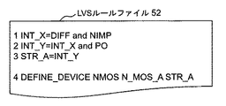
図12は図1の記憶装置4のデバイスレイアウトパターンファイル51に格納されるデバイスレイアウトパターンの構成例を示す平面図である。図12において、DIFF、PO、NIMP、PIMP、CONTは、それぞれトランジスタの拡散層、ポリシリコン、N+インプラント、P+インプラント、コンタクトの基本レイヤーである。デバイス名「N_MOS_A」のMOS電界効果トランジスタ(以下、MOSトランジスタという。)が、拡散層DIFFと、N+インプラントNIMPと、ポリシリコンPOが重なった領域として設定されている。また、このデバイスレイアウトパターンは、該当デバイスを構成するための必要最小限のレイヤーで描かれるとする。LVSルール比較修正処理の実行する前において、デバイスレイアウトパターンの入力時にデバイスレイアウトパターンにテキストで書かれたデバイス名と対応するレイヤー構成の情報を含むデバイスレイアウトパターンファイル51が記憶装置4に格納される。
FIG. 12 is a plan view showing a configuration example of the device layout pattern stored in the device
図13は図1の記憶装置4に格納されるLVSルールファイル52の具体例を示す図である。すなわち、図13では、LVSルール中のデバイス定義の一例を示す。一般に、LVSルールは使用するLVSツールに対応する入力形式に沿った記述をする必要がある。しかし、本質的には、デバイス定義に関しては、各デバイスに対応するレイヤー構成を論理式で設定し、それをデバイスの種類とデバイス名で関係付ける内容となっている。図13の1〜4行目ではそれぞれ以下のようにLVSルールを設定している。
FIG. 13 is a diagram showing a specific example of the
(1)拡散層DIFFと、N+インプラントNIMPとを論理積の形式で含む基本レイヤーINT_Xが設定される。
(2)基本レイヤーINT_Xと、ポリシリコンPOとを論理積の形式で含む中間レイヤーINT_Yが設定される。
(3)中間レイヤーINT_YからMOSトランジスタのデバイスSTR_Aが定義される。
(4)デバイスSTR_Aはデバイス名「N_MOS_A」のレイヤー構成として設定される。
(1) The base layer INT_X including the diffusion layer DIFF and the N + implant NIMP in the form of a logical product is set.
(2) An intermediate layer INT_Y including the basic layer INT_X and the polysilicon PO in the form of a logical product is set.
(3) A MOS transistor device STR_A is defined from the intermediate layer INT_Y.
(4) The device STR_A is set as a layer configuration of the device name “N_MOS_A”.
ここで、図13の4行目の「DEFINE_DEVICE」は、デバイス定義のためのLVSルールのコマンドを意味し、NMOSはデバイスの種類を示し、本例ではN型MOSトランジスタを示す。この例では、デバイス名「N_MOS_A」に対応するレイヤー「STR_A」は、拡散層DIFFと、N+インプラントNIMPと、ポリシリコンPOの論理積となっている。なお、LVSルール比較修正処理の実行する前において、LVSルールの入力時に、このデバイス名とレイヤー構成の情報を含むLVSルールファイル52が記憶装置4に格納される。
Here, “DEFINE_DEVICE” on the fourth line in FIG. 13 means an LVS rule command for device definition, NMOS indicates a device type, and in this example indicates an N-type MOS transistor. In this example, the layer “STR_A” corresponding to the device name “N_MOS_A” is a logical product of the diffusion layer DIFF, the N + implant NIMP, and the polysilicon PO. Before executing the LVS rule comparison / correction process, the
LVSルール比較修正処理では、デバイスレイアウトパターンファイル51内のデバイスレイアウトパターンから得られる各デバイスのレイヤー構成と、LVSルールファイル52内のLVSルールのデバイス定義から得られるレイヤー構成とを比較する。図12及び図13の例では、デバイスレイアウトパターンから得られるレイヤー構成である拡散層DIFFとN+インプラントNIMPとポリシリコンPOの重なりが、下記のレイヤー構成と一致する。当該レイヤー構成は、LVSルールのデバイス定義から得られる拡散層DIFFとN+インプラントNIMPとポリシリコンPOの論理積からなるレイヤー構成である。この場合において、LVSルール比較修正処理部50は、比較結果として「差分なし」を出力する。
In the LVS rule comparison and correction process, the layer configuration of each device obtained from the device layout pattern in the device
次いで、LVSルール比較修正処理では、比較結果が「差分あり」となる場合について図14A及び図14Bを参照して以下に説明する。図14A及び図14Bは図1の記憶装置4に格納されるLVSルールファイル52の具体例を示す図である。
Next, in the LVS rule comparison / correction process, a case where the comparison result is “with difference” will be described below with reference to FIGS. 14A and 14B. 14A and 14B are diagrams showing specific examples of the
ここで、図14AはLVSルール中のデバイス定義が誤っている場合の一例を示す。図14AのLVSルールを図13のLVSルールのデバイス定義と見比べると、図14Aの2行目において、中間レイヤーINT_YのポリシリコンPOに関する論理積が抜けていることが分かる。すなわち、ポリシリコンPOのレイヤーのないレイヤー「STR_A」でデバイス「N_MOS_A」が定義されている。この場合、図14AのLVSルールは、デバイスレイアウトパターンから得られるレイヤー構成である、拡散層DIFFとN+インプラントNIMPとポリシリコンPOの論理積と一致していない。従って、LVSルール比較修正処理部50は、比較結果として「差分あり」を出力する。
Here, FIG. 14A shows an example when the device definition in the LVS rule is incorrect. Comparing the LVS rule of FIG. 14A with the device definition of the LVS rule of FIG. 13, it can be seen that the logical product related to the polysilicon PO of the intermediate layer INT_Y is missing in the second row of FIG. 14A. That is, the device “N_MOS_A” is defined in the layer “STR_A” having no polysilicon PO layer. In this case, the LVS rule in FIG. 14A does not match the logical product of the diffusion layer DIFF, the N + implant NIMP, and the polysilicon PO, which is the layer configuration obtained from the device layout pattern. Accordingly, the LVS rule comparison /
また、LVSルール比較修正処理において、比較結果として「差分あり」となる別の場合について以下に説明する。図14Bは、LVSルール中のデバイス定義が誤っている場合の一例を示す。図13のLVSルールのデバイス定義と見比べると、図14Bの3行目において、デバイス「STR_A」の定義として、P+インプラントPIMPが中間レイヤーINT_Yに対して余分に論理積されていることが分かる。すなわち、N+インプラントNIMPもP+インプラントPIMPも重なったレイヤー「STR_A」でデバイス「N_MOS_A」が定義されている。この場合、レイヤー「STR_A」は、デバイスレイアウトパターンから得られるレイヤー構成である拡散層DIFFとN+インプラントNIMPとポリシリコンPOの論理積と一致していない。従って、LVSルール比較修正処理部50は比較結果として「差分あり」を出力する。
In the LVS rule comparison / correction process, another case in which “there is a difference” as a comparison result will be described below. FIG. 14B shows an example when the device definition in the LVS rule is incorrect. Compared with the device definition of the LVS rule in FIG. 13, in the third line of FIG. 14B, it can be seen that P + implant PIMP is logically ANDed with respect to the intermediate layer INT_Y as the definition of the device “STR_A”. That is, the device “N_MOS_A” is defined in the layer “STR_A” where the N + implant NIMP and the P + implant PIMP overlap. In this case, the layer “STR_A” does not coincide with the logical product of the diffusion layer DIFF, the N + implant NIMP, and the polysilicon PO, which is a layer configuration obtained from the device layout pattern. Therefore, the LVS rule comparison /
図15は図1の情報処理装置1により実行される比較処理(S41)の具体例を示す図である。図15において、図1の比較情報ファイル54の具体例を示す。
FIG. 15 is a diagram showing a specific example of the comparison process (S41) executed by the
図15において、デバイスレイアウトパターンファイル51は、デバイス名「N_MOS_A」、「N_MOS_B」、「N_MOS_C」、及び「N_MOS_D」に対応する4種類のデバイスのレイアウトパターンを格納している。これに対して、LVSルールファイル52には、この4種類のデバイスに対応するデバイス定義が書かれている。LVSルール比較修正処理部50は、この両データで設定されている各デバイスのレイヤー構成を比較し、その結果を比較情報ファイル54として出力する。本例では、デバイス名「N_MOS_A」と「N_MOS_B」との間でレイヤー構成が一致し、「MATCHED」と出力されているが、デバイス名「N_MOS_C」と「N_MOS_D」との間でレイヤー構成に不一致がある結果となっている。その不一致の内容は、デバイス名「N_MOS_C」に関しては、対応するLVSルールにおいてポリシリコンPOのレイヤーが未定義である点にある。また、デバイス名「N_MOS_D」に関しては、LVSルールにおいてP+インプラントPIMPのレイヤーが過剰に定義されて比較情報として出力されている。LVSルールの開発者は、この比較情報から、LVSルールのどのデバイスのレイヤー構成に誤りがあるかを容易に把握することができる。
In FIG. 15, a device layout pattern file 51 stores layout patterns of four types of devices corresponding to device names “N_MOS_A”, “N_MOS_B”, “N_MOS_C”, and “N_MOS_D”. On the other hand, in the
さらに、デバイス定義のレイヤー構成に「論理否定」が含まれている場合のデバイスレイアウトパターンに対する比較処理(S41)について以下に説明する。 Further, the comparison process (S41) for the device layout pattern when “logical negation” is included in the device definition layer configuration will be described below.
図16は図1の記憶装置4に格納されるLVSルールファイル52の具体例を示す図である。ここで、図16は、LVSルールのデバイス定義において、レイヤー構成に「論理否定」が含まれている一例である。図16のデバイス定義を、図13のデバイス定義と見比べると、図16の3行目において、レイヤー「STR_A」に対する論理式で、「not LAY_A」が付加されていることが分かる。すなわち、レイヤー「LAY_A」との重なりを持たないレイヤー「INT_Y」をデバイス名「N_MOS_A」のレイヤー構成としている。このようなデバイス定義の場合、図12で示したデバイスレイアウトパターンだけでは十分ではなく、比較処理(S41)によりLVSルールファイル52の検証ができない。なぜなら、図12で示したデバイスレイアウトパターンには、レイヤー「LAY_A」に関する指定がなされていないからである。このようなデバイス定義を持つデバイスの場合のデバイスレイアウトパターンの構成例を図17A及び図17Bに示す。
FIG. 16 is a diagram showing a specific example of the
図17A及び図17Bは、図1の記憶装置4のデバイスレイアウトパターンファイル51に格納されるデバイスレイアウトパターンの具体例を示す平面図である。ここで、図17Aは、図12と同一のデバイス名「N_MOS_A」のデバイスレイアウトパターンを示し、デバイス認識に必要な最小限のレイヤーの構成要素、すなわち、拡散層DIFFとN+インプラントNIMPとポリシリコンPOが描かれている。図17Bは、図17Aに対してレイヤー「LAY_A」が重畳されたものである。比較処理(S41)では、この両デバイスレイアウトパターンを読み取り、その差分のレイヤーが論理否定として、LVSルールのデバイス定義に含まれているかをチェックする。このチェック処理について具体例を用いて以下に説明する。
17A and 17B are plan views showing specific examples of device layout patterns stored in the device
デバイスレイアウトパターンファイル51のデータ読み取り時に、デバイス「N_MOS_A」を構成する必要最小限のレイヤーで描かれた図17Aからレイヤー構成が拡散層DIFFとN+インプラントNIMPとポリシリコンPOの重なりであることを読み取る。次に、図17Bの「NOT」(論理否定のコマンド)とテキストで書かれたデバイスレイアウトパターンのレイヤー構成、すなわち、拡散層DIFFとN+インプラントNIMPとP+インプラントPOとレイヤー「LAY_A」を読み取る。なお、以下では、図17Bのように、「NOT」と記されたデバイスレイアウトパターンを「NOTデバイスレイアウトパターン」という。
When reading the data of the device
次に、図17Aのレイヤー構成と、図17Bのレイヤー構成の差分をとると、差分結果はレイヤー「LAY_A」となり、その論理否定、すなわち、「not LAY_A」の処理が、LVSルールファイル52のデバイス定義に含まれているかをチェックする。図16、図17A、及び図17Bの例では、図17A及び図17Bのデバイスレイアウトパターンから得られるレイヤー「LAY_A」が、図16のLVSルールのデバイス定義の3行目において、確かに、その論理否定「not LAY_A」として定義されている。LVSルール比較修正処理部50は、この場合、比較結果として「差分なし」を出力する。なお、この例では、論理否定のレイヤーは、「LAY_A」のみとしたが、複数のレイヤーあってもかまわない。その場合には、それぞれの論理否定のレイヤーを重畳したデバイスレイアウトパターンを「NOTデバイスレイアウトパターン」として複数個用意する。もしくは、関係する論理否定のレイヤーを全て重畳したデバイスレイアウトパターンを「NOTデバイスレイアウトパターン」として一つ用意すればよい。
Next, when the difference between the layer configuration of FIG. 17A and the layer configuration of FIG. 17B is taken, the difference result is layer “LAY_A”, and the logical negation, that is, the process of “not LAY_A” is Check if it is included in the definition. In the example of FIG. 16, FIG. 17A and FIG. 17B, the layer “LAY_A” obtained from the device layout pattern of FIG. 17A and FIG. 17B is certainly the logic in the third line of the device definition of the LVS rule of FIG. It is defined as negation “not LAY_A”. In this case, the LVS rule comparison /
さらに、LVSルール比較修正処理部50によるLVSルール修正処理(S44)について具体例を用いて説明する。差分有無の判断処理(S42)において差分があった場合、図15に一例として示されているような、差分情報を含む比較情報が得られる。上述のように、この比較情報には、以下の2つの場合がある。
(1)デバイス名「N_MOS_C」のデバイス定義においてポリシリコンPOのレイヤーが未定義のため、「不一致」となっている場合。
(2)デバイス名「N_MOS_D」のデバイス定義においてP+インプラントPIMPが過剰に定義されているために不一致となっている場合。
Furthermore, the LVS rule correction process (S44) by the LVS rule comparison /
(1) The device definition of the device name “N_MOS_C” is “unmatched” because the polysilicon PO layer is undefined.
(2) A case where the device definition of the device name “N_MOS_D” is inconsistent because P + implant PIMP is excessively defined.
LVSルール修正処理(S44)では、この比較情報を元に、LVSルールファイル52のデバイス定義の修正を行う。その修正内容に関して、図18A、図18B及び図19を参照して具体例を示す。
In the LVS rule correction process (S44), the device definition of the
図18Aは図1の記憶装置4に格納される修正前のLVSルールファイル52の具体例を示す図である。また、図18Bは図1の記憶装置4に格納される修正後LVSルールファイル53の具体例を示す図である。ここで、図18Aは、デバイス「N_MOS_C」に関する修正前のLVSルールファイル52であり、デバイス名「N_MOS_C」のレイヤー構成であるレイヤー「STR_C」にポリシリコンPOのレイヤーが含まれていない。LVSルール修正処理(S44)では、デバイス名「N_MOS_C」のデバイス定義でポリシリコンPOのレイヤーが未定義である比較情報から、図18Bに示すようにポリシリコンPOのレイヤーの論理積を加える処理をLVSルールファイル52に対して行う。そして、修正後のLVSルールを含む修正後LVSルールファイル53を出力する。
18A is a diagram showing a specific example of the
図19Aは図1の記憶装置4に格納される修正前のLVSルールファイル52の具体例を示す図である。また、図19Bは図1の記憶装置4に格納される修正後LVSルールファイル53の具体例を示す図である。ここで、図19Aは、デバイス「N_MOS_D」に関する修正前のLVSルールファイル52であり、デバイス名「N_MOS_D」のレイヤー構成であるレイヤー「STR_D」P+インプラントPIMPのレイヤーが余計に含まれている。LVSルール修正処理では、デバイス名「N_MOS_D」のデバイス定義でレイヤーPIMPが過剰に定義されているという比較情報から図19Bに示すようにP+インプラントPIMPのレイヤーの論理積を除去する処理をLVSルールファイル52に対し行う。そして、修正後のLVSルールを含む修正後LVSルールファイル53を出力する。
FIG. 19A is a diagram showing a specific example of the
以上の実施形態においては、半導体集積回路のレイアウトを検証する際に使用されるレイアウト検証用ルールを検証する際に使用されるレイアウト検証用パターンをレイアウト検証用ルールと比較して比較結果である差分を含む比較情報を生成する比較処理を備える。また、情報処理装置1は上記差分があるときに、上記比較情報に基づいて上記レイアウト検証用ルールを修正する修正処理をさらに備える。本発明はこれに限らず、情報処理装置1は比較処理のみを備えて構成してもよい。
In the above embodiment, the difference, which is the comparison result, is obtained by comparing the layout verification pattern used when verifying the layout verification rule used when verifying the layout of the semiconductor integrated circuit with the layout verification rule. The comparison process which produces | generates the comparison information containing is provided. The
以上説明したように、本実施形態にかかる情報処理装置1によれば、レイアウト検証用DRCルール又はLVSルールの検証工程において、従来技術に比較して修正処理の工数を削減でき、当該ルールの修正効率を高めることができる。
As described above, according to the
また、LVSルールの検証工程において、LVSルールは、論理積と論理否定、又は論理積を含む論理式を用いて定義されている。これにより、当該論理式を用いて表されたLVSルールの比較、修正が可能になる。 In the LVS rule verification process, the LVS rule is defined using a logical expression including a logical product and a logical negation or a logical product. This makes it possible to compare and modify LVS rules expressed using the logical expressions.
変形例1.
図20は図1の情報処理装置1により実行される変形例1に係る比較処理(S41A)の具体例を示す図である。以上の実施形態では、デバイスレイアウトパターンファイル51とLVSルールファイル52Aの個数が一対一で対応している場合を述べてきたが、この対応が取れていない場合の比較処理について以下に説明する。すなわち、デバイスレイアウトパターンで設定されているパターン数以上に、LVSルールファイル52Aにおいてデバイス定義がある場合とない場合の扱いについてである。このとき、比較工程(S41A)において、対応するLVSルールファイルのデバイス定義の過不足の情報を出力する。これについて、図20を参照して以下に説明する。
FIG. 20 is a diagram illustrating a specific example of the comparison process (S41A) according to the first modification executed by the
図20の比較情報ファイル54Aは、LVSルールファイル52Aにおいて、本来設定されているべきデバイス定義がなされていない場合の具体例を示す。ここで、LVSルールファイル52Aにおいて、デバイスレイアウトパターンファイル51で設定されている「N_MOS_D」に対応するデバイス定義の設定がない。このとき、比較処理S51Aにおいて、この差異を検出し、その結果を比較情報ファイル54Aとして出力する。この例では、デバイス名「N_MOS_A、N_MOS_BとN_MOS_C」においてはレイヤー構成が一致し、「MATCHED」と出力されている。しかし、デバイス名「N_MOS_D」においては対応するデバイス定義がない旨(N_MOS_D:NOT DEFINED, STR_D)が出力されている。LVSルールの開発者は、この比較情報ファイル54Aから、LVSルールファイル52Aにおいてデバイス定義の抜けがあることを容易に把握できる。比較情報ファイル54Aにおける、デバイス名「STR_D」は、デバイスレイアウトパターンファイル51から抽出されるデバイス名「N_MOS_D」に対応する構成レイヤーであり、一般には論理式で記述されるものであり、修正処理で用いる情報となる。
The comparison information file 54A of FIG. 20 shows a specific example when the device definition that should originally be set is not made in the LVS rule file 52A. Here, in the LVS rule file 52A, there is no device definition setting corresponding to “N_MOS_D” set in the device
図21は図20の比較処理(S41A)の後の修正処理により修正された修正後LVSルールファイル53Aの具体例を示す図である。 FIG. 21 is a diagram showing a specific example of the modified LVS rule file 53A modified by the modification processing after the comparison processing (S41A) of FIG.
図20の比較処理(S41A)の後の修正処理では、比較情報ファイル54Aを用いて、LVSルールファイル52Aの修正を行う。具体的には、比較情報ファイル54Aに未設定デバイスのデバイス名とその構成レイヤーが示されている。この内容をLVSルールファイル52Aにデバイス定義文として、例えば、「DEFINE_DEVICE NMOS N_MOS_D STR_D」の記述を追加する。すなわち、LVSルールファイル52Aにデバイス定義の抜けがあっても、この修正処理を経ることで、デバイスレイアウトパターンファイル51に一対一で対応した図21の修正後LVSルールファイル53Aを得ることができる。
In the correction process after the comparison process (S41A) in FIG. 20, the LVS rule file 52A is corrected using the comparison information file 54A. Specifically, the comparison information file 54A shows the device name of the unset device and its configuration layer. For example, a description of “DEFINE_DEVICE NMOS N_MOS_D STR_D” is added as a device definition statement to the LVS rule file 52A. That is, even if there is a missing device definition in the LVS rule file 52A, the modified LVS rule file 53A of FIG. 21 corresponding to the device
変形例2.
図22は図1の情報処理装置1により実行される変形例2に係る比較処理(S41B)の具体例を示す図である。図22の比較情報ファイル54Bは、LVSルールファイル52Bにおいて、本来設定の必要のないデバイス定義がなされている場合の具体例を示す。
FIG. 22 is a diagram illustrating a specific example of the comparison process (S41B) according to the second modification executed by the
図22のLVSルールファイル52Bにおいて、デバイスレイアウトパターンファイル51で設定されていないデバイス名「N_MOS_E」に対応するデバイス定義が設定されている。比較処理(S41B)では、この差異を検出し、その結果を比較情報ファイル54Bに出力する。この例では、デバイス名「N_MOS_A」、「N_MOS_B」、「N_MOS_C」と「N_MOS_D」においてはレイヤー構成が一致し、「MATCHED」と出力されている。しかし、デバイス名「N_MOS_E」においては過剰なデバイス定義である旨(N_MOS_E:OVER DEFINED)が出力されている。LVSルールの開発者は、この比較情報ファイル54Bから、LVSルールファイル52Bにおいて余分なデバイス定義があることを容易に把握できる。
In the LVS rule file 52B of FIG. 22, a device definition corresponding to the device name “N_MOS_E” not set in the device
図23は図22の比較処理(S41B)の後の修正処理により修正された修正後LVSルールファイル53Bの具体例を示す図である。 FIG. 23 is a diagram showing a specific example of the modified LVS rule file 53B modified by the modification process after the comparison process (S41B) of FIG.
図22の比較処理(S41B)の後の修正処理では、比較情報ファイル54Bを用いて、LVSルールファイル52Bの修正を行う。具体的には、比較情報ファイル54Bに過剰設定されたデバイスのデバイス名が示されており、対応するデバイス定義の記述をLVSルールファイル52Bから削除する。具体的には、LVSルールファイル52Bにおいて、「DEFINE_DEVICE NMOS N_MOS_E STR_E」が削除される。すなわち、LVSルールファイル52Bに本来必要のないデバイス定義があっても、この修正処理を経ることで、デバイスレイアウトパターンファイル51に一対一で対応した図23の修正後LVSルールファイル53Bを得ることができる。
In the correction process after the comparison process (S41B) in FIG. 22, the LVS rule file 52B is corrected using the comparison information file 54B. Specifically, the device name of the over-set device is shown in the comparison information file 54B, and the corresponding device definition description is deleted from the LVS rule file 52B. Specifically, “DEFINE_DEVICE NMOS N_MOS_E STR_E” is deleted from the LVS rule file 52B. That is, even if there is a device definition that is not originally required in the LVS rule file 52B, the modified LVS rule file 53B of FIG. 23 corresponding to the device
1…情報処理装置、
2…キーボード、
3…マウス、
4…記憶装置、
10…DRCルール比較修正処理部、
11…テストパターンファイル、
12…DRCルールファイル、
13…修正後DRCルールファイル、
14…比較情報ファイル、
50…LVSルール比較修正処理部、
51…デバイスレイアウトパターンファイル、
52,52A,52B…LVSルールファイル、
53,53A,53B…修正後LVSルールファイル、
54,54A,54B…比較情報ファイル。
1 Information processing device,
2 ... Keyboard,
3 ... mouse,
4 ... Storage device,
10 ... DRC rule comparison and correction processing unit,
11 ... Test pattern file,
12 ... DRC rule file,
13 ... The modified DRC rule file,
14 ... Comparison information file,
50 ... LVS rule comparison and correction processing unit,
51 ... Device layout pattern file,
52, 52A, 52B ... LVS rule file,
53, 53A, 53B ... LVS rule file after modification,
54, 54A, 54B: Comparison information file.
Claims (12)
上記レイアウト検証用ルールを検証する際に使用されるレイアウト検証用パターンを、上記レイアウト検証用ルールと比較し、比較結果である差分を含む比較情報を生成する比較手段を備えたことを特徴とする情報処理装置。 In an information processing apparatus for verifying a layout verification rule used when verifying a layout of a semiconductor integrated circuit,
Comparing means for comparing a layout verification pattern used when verifying the layout verification rule with the layout verification rule, and generating comparison information including a difference as a comparison result. Information processing device.
上記レイアウト検証用ルールがレイアウト検証用デザインルールであるとき、上記レイアウト検証用パターンはレイアウト検証用テストパターンであり、
上記レイアウト検証用ルールがレイアウト検証用デバイスレイアウトルールであるとき、上記レイアウト検証用パターンはレイアウト検証用デバイスレイアウトパターンであることを特徴とする請求項1又は2記載の情報処理装置。 The layout verification rule is at least one of a layout verification design rule and a layout verification device layout rule.
When the layout verification rule is a layout verification design rule, the layout verification pattern is a layout verification test pattern,
3. The information processing apparatus according to claim 1, wherein when the layout verification rule is a layout verification device layout rule, the layout verification pattern is a layout verification device layout pattern.
上記処理手段が、上記レイアウト検証用ルールを検証する際に使用されるレイアウト検証用パターンを、上記レイアウト検証用ルールと比較し、比較結果である差分を含む比較情報を生成するステップを含むことを特徴とする情報処理方法。 In an information processing method executed by an information processing apparatus including a processing unit for verifying a layout verification rule used when verifying a layout of a semiconductor integrated circuit,
The processing means includes a step of comparing a layout verification pattern used when verifying the layout verification rule with the layout verification rule, and generating comparison information including a difference as a comparison result. A characteristic information processing method.
上記処理手段が、上記レイアウト検証用ルールを検証する際に使用されるレイアウト検証用パターンを、上記レイアウト検証用ルールと比較し、比較結果である差分を含む比較情報を生成するステップを含むことを特徴とするプログラム。 In a program executed by an information processing apparatus having a processing means for verifying a layout verification rule used when verifying a layout of a semiconductor integrated circuit,
The processing means includes a step of comparing a layout verification pattern used when verifying the layout verification rule with the layout verification rule, and generating comparison information including a difference as a comparison result. A featured program.
Applications Claiming Priority (4)
| Application Number | Priority Date | Filing Date | Title |
|---|---|---|---|
| JP2015133692 | 2015-07-02 | ||
| JP2015133692 | 2015-07-02 | ||
| JP2016039641 | 2016-03-02 | ||
| JP2016039641 | 2016-03-02 |
Publications (1)
| Publication Number | Publication Date |
|---|---|
| JP2017162429A true JP2017162429A (en) | 2017-09-14 |
Family
ID=59854181
Family Applications (1)
| Application Number | Title | Priority Date | Filing Date |
|---|---|---|---|
| JP2016107545A Pending JP2017162429A (en) | 2015-07-02 | 2016-05-30 | Information processing device and method, and program |
Country Status (1)
| Country | Link |
|---|---|
| JP (1) | JP2017162429A (en) |
Cited By (1)
| Publication number | Priority date | Publication date | Assignee | Title |
|---|---|---|---|---|
| CN113627122A (en) * | 2021-08-12 | 2021-11-09 | 长鑫存储技术有限公司 | Test pattern verification method, device, equipment and storage medium |
-
2016
- 2016-05-30 JP JP2016107545A patent/JP2017162429A/en active Pending
Cited By (2)
| Publication number | Priority date | Publication date | Assignee | Title |
|---|---|---|---|---|
| CN113627122A (en) * | 2021-08-12 | 2021-11-09 | 长鑫存储技术有限公司 | Test pattern verification method, device, equipment and storage medium |
| CN113627122B (en) * | 2021-08-12 | 2024-01-23 | 长鑫存储技术有限公司 | Verification method, device and equipment of test pattern and storage medium |
Similar Documents
| Publication | Publication Date | Title |
|---|---|---|
| US7284214B2 (en) | In-line XOR checking of master cells during integrated circuit design rule checking | |
| JP4745256B2 (en) | Pattern creation method, pattern creation / verification program, and semiconductor device manufacturing method | |
| JP2007265179A (en) | Layout verification method, and layout verification unit | |
| CN105740494B (en) | Electronic design automation method and device thereof | |
| JP2008009964A (en) | Layout making equipment and method of making layout of semiconductor integrated circuit | |
| US7464350B1 (en) | Method of and circuit for verifying a layout of an integrated circuit device | |
| US9934349B2 (en) | Method for verifying design rule checks | |
| US8645876B2 (en) | Methodology for performing post layer generation check | |
| US10628550B2 (en) | Method for designing an integrated circuit, and method of manufacturing the integrated circuit | |
| CN105718623B (en) | Method and system for generating semiconductor circuit layout | |
| JP2017162429A (en) | Information processing device and method, and program | |
| US20160342728A1 (en) | Visualization Of Analysis Process Parameters For Layout-Based Checks | |
| JP5293521B2 (en) | Design rule check verification apparatus and design rule check verification method | |
| JP4774237B2 (en) | Program development support apparatus, program operation comparison method, and semiconductor integrated circuit manufacturing method | |
| JP2009026045A (en) | Layout creating device and manufacturing method for semiconductor integrated circuit | |
| US8751988B1 (en) | Computer-implemented methods and systems for automatic generation of layout versus schematic (LVS) rule files and regression test data suites | |
| US9754067B2 (en) | Method of checking the layout integrity | |
| US20120072877A1 (en) | Layout verification apparatus and layout verification method | |
| US20060090144A1 (en) | Method of automating place and route corrections for an integrated circuit design from physical design validation | |
| US20110119544A1 (en) | User Guided Short Correction And Schematic Fix Visualization | |
| JP2008262356A (en) | Layout creation apparatus and method for semiconductor integrated circuit | |
| US20160267217A1 (en) | Display apparatus and design method of semiconductor integrated circuit | |
| US20120192134A1 (en) | User Guided Short Correction And Schematic Fix Visualization | |
| JP5663380B2 (en) | Layout verification apparatus and layout verification method | |
| US9330229B2 (en) | Optical proximity correction verification system and verification method thereof |